
Analysis and Design of a Wireless Power Transfer System with Dual Active Bridges


1
Key Laboratory of Control of Power Transmission and Transformation Ministry of Education, Shanghai Jiao Tong University, 800 Dongchuan RD., Shanghai 200240, China
2
College of Electric and Information Engineering, Zhengzhou University of Light Industry, Zhengzhou 450002, China
*
Author to whom correspondence should be addressed.
Energies 2017, 10(10), 1588; https://doi.org/10.3390/en10101588
Submission received: 25 August 2017
/
Revised: 30 September 2017
/
Accepted: 9 October 2017
/
Published: 12 October 2017
Abstract
:Nowadays, work on Wireless Power Transfer (WPT) systems with dual active bridges is attracting great attention due to their low conduction losses, power regulation, load transformation and reactance compensation. However, in these studies limitations such as overall analysis, design and realization techniques of the system were not considered properly. To address the aforementioned issues, this paper presents a detailed analysis, design and realization of a Series-Series (SS) WPT system with dual active bridges, which will improve the overall performance. Three independent Phase Angles (PAs) have been analyzed and designed in this study, one PA on the primary side and the other two PAs on the secondary side. This Multiple Degrees of Phase Control (MDPC) method can achieve additional reactance compensation, load transformation and output regulation simultaneously. To realize the proposed method in practice, key implementation techniques have been investigated in detail, including additional reactance estimation, mutual inductance estimation, phase detection and synchronization. The feasibility and effectiveness of the proposed system is verified through simulation and experimental results.
1. Introduction
Wireless Power Transfer (WPT) systems can utilize coupling coils to transfer energy through magnetic fields, which can avoid the physical connection of charging lines. Due to their convenience and possibility of widespread applications, the WPT technique has been the research focus of many studies [1,2]. Various wireless charging devices have been invented and manufactured for use in applications such as portable consumer electronics and electric vehicles [3,4,5,6].
Compensation capacitors are indispensable elements of a WPT system [1]. These capacitors compensate the inductive reactance of the transmitting and receiving coils, and contribute significantly to inducing a meaningful amount of current needed for sufficient magnetic field generation. In order to realize strongly coupled magnetic resonance [1,7], the ideal method is to tune the transmitter and receiver at the same resonance frequency. Although capacitor arrays can be used, they require many capacitors, switches and complex control algorithms. Furthermore, high voltage stresses on the resonant capacitors require large packaging and capacitors have large manufacturing tolerances. In addition, the capacitances and the coil inductances vary due to aging. Hence, it is a challenge to select the capacitors with ideal capacitance and rated voltage [8,9,10]. When non-identical resonances occur, the additional reactance increases apparent power and causes additional losses. Thus, extra input power is required at the same load which causes a lower efficiency.
Maximum power transfer efficiency is achieved when the load matches with the system [7,11]. In a Series-Series (SS) WPT system, a small loading resistance results in most losses consumed by the receiving coil, whereas a large loading resistance leads to a small reflected resistance and most of the energy is wasted in the transmitting coil. In [9,12], a cascaded buck-boost converter is utilized for load transformation. An improved efficiency of 78% with a 16 W transferred power at a distance of 10 cm is achieved in [12], whereas [9] realizes an efficiency of 65% when delivering 4.5 W power. In [13], a two-stage switching converter is applied to modulate the load, an efficiency of 60.2% is obtained for a 20-W load at 20 cm. In [14], the concept of phase-shift and amplitude control is introduced to modify the equivalent secondary-side load impedance for efficiency enhancement and extractable power optimization. The amplitude control is realized by an additional buck converter on the receiver side. The measured maximum efficiency is 77.3% when the coupling factor is 0.6. In [15], a front-end boost circuit and a rear-end buck circuit are employed for voltage regulation and load transformation, respectively. The optimal efficiency is 79% when 100 W power is delivered at 20 cm, with 6% power loss measured in DC-DC converters. Compared with traditional systems, these topologies help to transform the load to the optimal value and contribute to improving the efficiency. However, the control of multi-stage system is complex and additional losses in the converters are inevitable. In addition, they can increase the size of the receiver. Greater focus on finding a better solution is needed.
Adding an active rectifier on the receiver side has been proposed in [14,16]. Furthermore, researchers have found that Phase Control (PC) can be employed for conduction loss reduction and bidirectional power flow regulation [17,18,19]. In [16], two Phase Angles (PAs) are applied to regulate dual-side resonant currents equally to reduce losses. However, the de-tuning of the WPT system is not taken into consideration and parasitic resistances are omitted in the analysis. Researchers in [14,20,21] realized that PC can change the effective voltage applied on the resonant tank and the resulting equivalent impedance seen from the AC side. In [14], the equivalent impedance is regarded as an optimization function and the mathematical expression of the equivalent impedance is not presented. In [20], a semi-bridgeless active rectifier is investigated and the output power can be regulated by secondary PC. In addition, the equivalent impedance of the semi-bridgeless active rectifier is derived. Both of [14] and [20] majorly focus on the proposal of the concept and its derivation, whereas the implementation techniques are not rigorously studied. Researchers in [21] demonstrate PC from the standpoint of load transformation and additional reactance compensation that achieves a maximum efficiency rise of 10% compared with traditional diode rectifier. An Auxiliary Measurement Coil (AMC) along with a decoupling transformer is adopted to detect the additional reactance. The decoupling transformer is used to cancel out the voltage induced by the receiver side current to the measurement circuit. Therefore, two mutual inductances, one between the receiving coil and AMC and the other of the transformer, should be identical. However, mutual inductance is strongly affected by the inductances, the position of the coils and its surroundings. It is difficult to ensure that two mutual inductances have equal values in experiments. Discrepancy of mutual inductances can bring about an estimation error in principle. In addition, the measurement of mutual inductance, which is an important parameter for optimal load calculation, is not presented. Although a real-time mutual inductance estimation method has been proposed in [22], it assumes that the WPT system is tuned completely. In [23], mutual inductance estimation is implemented by detecting primary PA. Nevertheless, when the system operates at secondary resonant frequency, a large estimation error appears. Further work on additional reactance and mutual inductance estimations is required.
Synchronization is an important technique in the control of secondary PC. Researchers in [18] proposed an AMC for synchronization. However, over 20% phase error occurs at 20 kHz when the load or the mutual inductance changes. In [21], a current sensor is used to capture the secondary resonant current for synchronization at 30 kHz. Since the current measurement and filtering process involve a significant time delay, a phase-shift circuit should be adopted to correct the resulting phase error. In addition, current sensors have band limits, generally lower than 100 kHz. The synchronization may be more difficult with a higher operating frequency. Therefore, improvement of the synchronization technique is necessary.
This paper presents a detailed analysis and design of a WPT system with dual active bridges. Multiple Degrees of Phase Control (MDPC) are adopted. The system has three degrees of control freedom. Primary PA is responsible for voltage regulation, and secondary PAs for load transformation as well as additional reactance compensation. The proposed additional reactance and mutual inductance estimation methods are based on DC voltage and current samplings, which are easy to be implemented. An effective phase detection technique is elaborated where the phase information is modulated onto a DC voltage signal. In addition, a novel synchronization technique involving a comparator and an isolator is proposed that works satisfactorily at a frequency of 100 kHz. It is simpler and cheaper than previous methods and can withstand parameter variations.
2. Modeling of Wireless Power Transfer (WPT) System
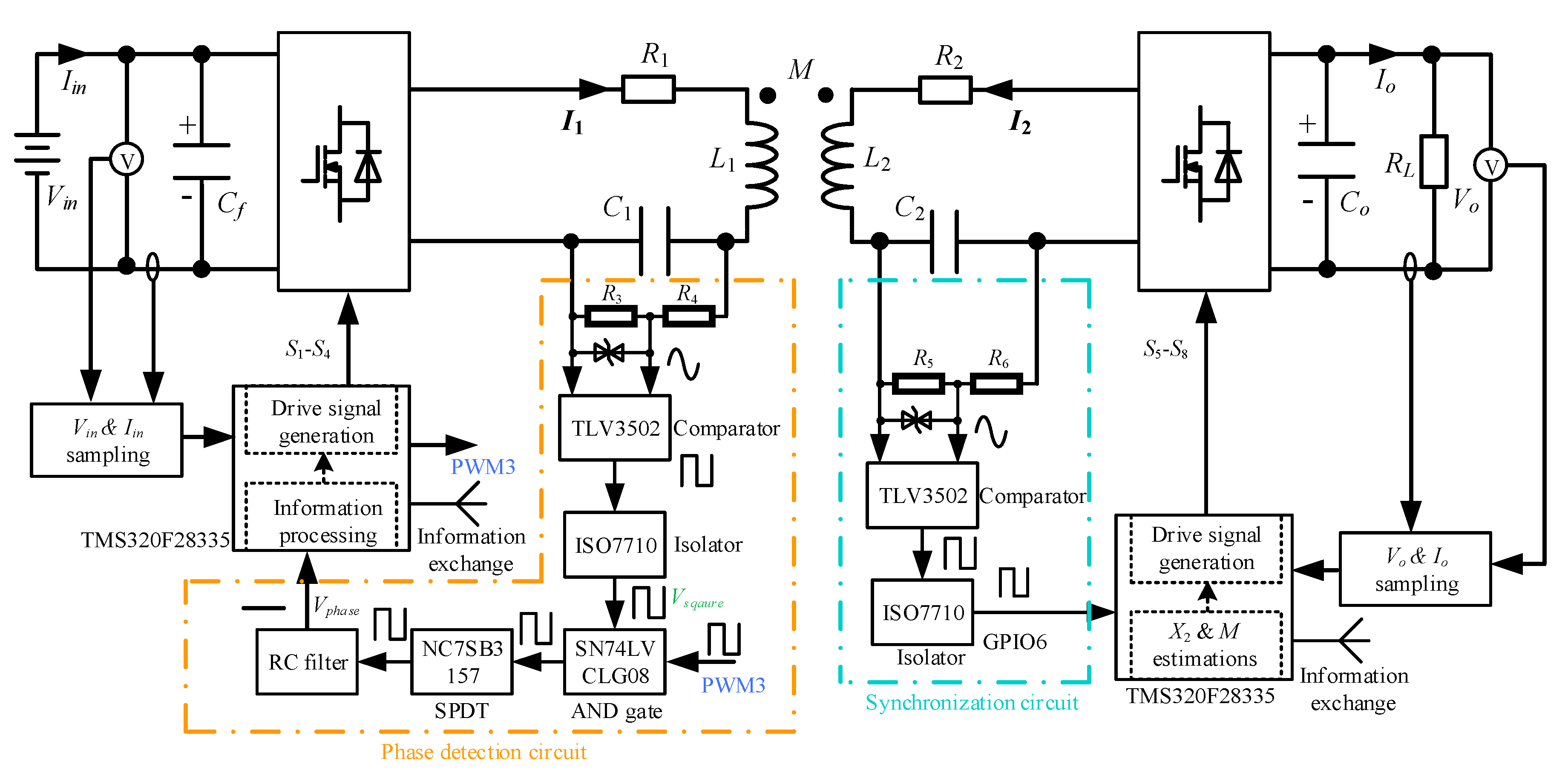
The schematic and equivalent circuit of the proposed system are shown in Figure 1. In this paper, bold italic letters represent the phasors, whereas italic letters symbolize real numbers or Root-Mean-Square (RMS) values of the phasors. Vin is the input voltage and Iin is the input current. Cf is the film capacitor which makes the inverter decoupled and the input current stable. Q1–Q8 are the Metal-Oxide-Semiconductor Field-Effect Transistors (MOSFETs) of two active bridges. L1 and L2 are the inductances of the transmitting and receiving coils, whose parasitic resistances are R1 and R2, respectively. C1 and C2 are the compensation capacitors, and Co is the output filtering capacitor. RL represents the loading resistance and Vo is the voltage across it. Ze is the equivalent impedance, whose real part and imaginary part are denoted as Re and Xe, respectively. The primary resonant angular frequency ω1, the secondary resonant angular frequency ω2, the primary reactance X1, and the secondary reactance X2 are defined as:
Uncontrolled rectification is utilized in most WPT systems [7,9,12,24]. The analysis presented is based on full load conditions and the output filtering capacitor is supposed to be large enough to maintain a stable output DC voltage. Thus, the equivalent impedance Ze is purely resistive [7,9]:
The system operates at primary resonance frequency (f = f1), that is, X1 = 0. Based on the Kirchhoff voltage law, current loops are drawn as:
The power transfer efficiency η is defined as:
where Re represents the real part of the phasor.
By combining Equations (3) and (4), η is derived:
The three dimensional plot of the power transfer efficiency η as a function of the load RL and the additional reactance X2 is shown in Figure 2. The related parameters are listed in Table 1. The efficiency increases with the increase of |X2| at a constant RL. The existence of additional reactance causes a larger apparent power, resulting in more losses consumed by the parasitic resistances. Thus, the higher |X2| and the lower η. By taking partial derivative of X2, it is deduced that η reaches the peak when X2 = 0. However, the efficiency keeps varying with the load. The calculated efficiency is 49.9% when RL = 998 Ω, which is required for maximum power transfer capability. Whereas, the efficiency is 95.2% when RL = 24.8 Ω, which is required for maximum power transfer efficiency [9]. Figure 2 clearly illustrates the importance of additional reactance compensation and load transformation for efficiency enhancement.
3. Multiple Degrees of Phase Control
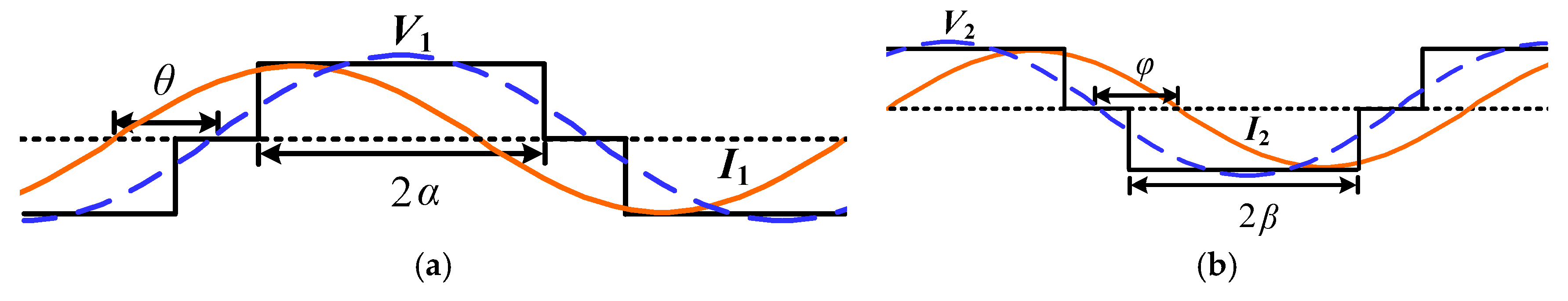
Figure 3 shows the square-wave voltages, fundamental voltages and resonant currents of two active bridges used in the SS WPT system. As can be seen from Figure 3, there are two PAs in each bridge, thus the total PAs of the system are four. θ is the PA between primary fundamental voltage and I1. φ is the PA between the secondary fundamental voltage and I2. α and β are the PAs of the primary and secondary bridge arms, respectively. φ changes the impedance of the receiver and the corresponding primary reflected load, resulting in the alteration of θ. Hence, there only exist three independent and controllable PAs, they are: α, β and φ. Voltage regulation, load transformation and additional reactance compensation can be realized simultaneously by full utilization of these three PAs.
3.1. Equivalent Impedance Derivation
The equivalent impedance of the transmitter (Zin) is:
Thus, θ can be affected by the reflected resistive and reactive components back on the primary side. In other words, there are only three independent and controllable PAs including α, β and φ. When the secondary additional reactance is compensated (X2 + Xe = 0), Zin is resistive even when Xe 0. According to (6), the optimal load depends on the mutual inductance. When M changes due to the offset of the coils, the corresponding optimal PAs vary. This paper aims to reduce the efficiency degradation caused by parameter variations. On-line estimations can be applied to detect these changes, which can adapt to the mutual inductance and load variations.
Some systems operate at ω2 and regulate the power flow by the PA between the primary and secondary voltage phasors [17,25]. It can introduce reactive power into the system and bring about undesired efficiency degradation. The proposed system operates at ω1 and utilizes φ to compensate secondary additional reactance X2. Power regulation and load transformation are realized by regulation of α and β, respectively. This strategy reduces the reactive power that would otherwise be present.
To obtain the optimal efficiency point, the additional reactance should be compensated completely and the load should be transformed to the optimal value. Hence, the mathematical expressions of the equivalent reactance and resistance of the receiver should be derived.
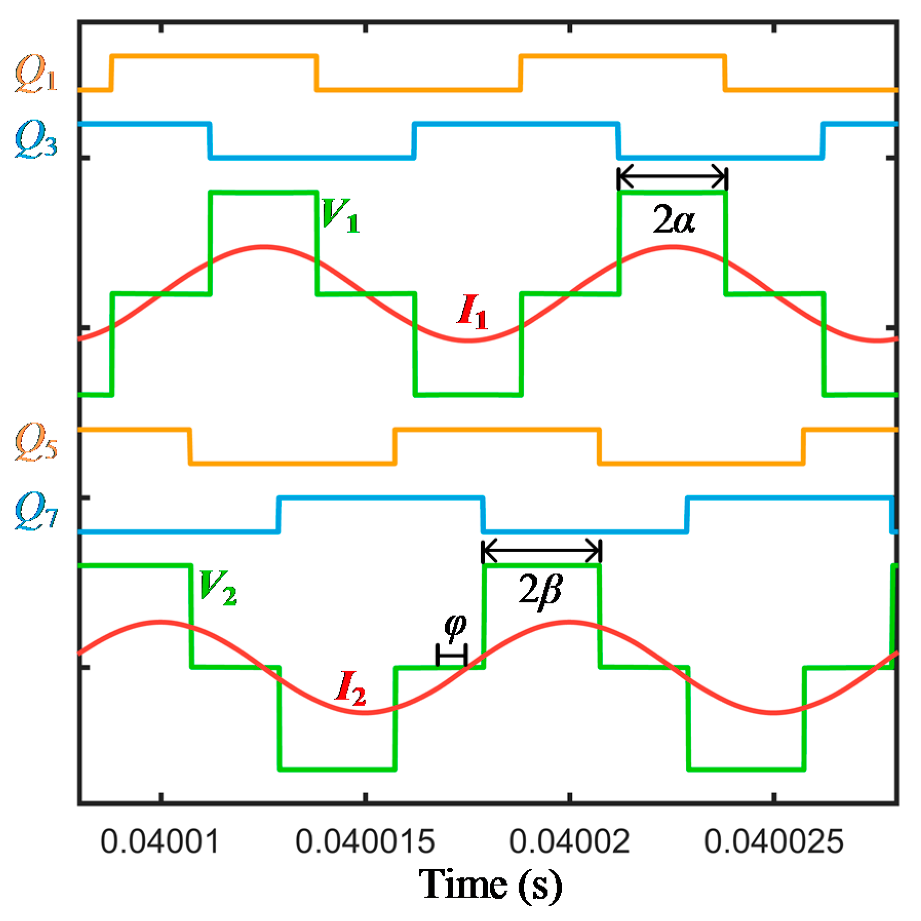
Figure 4 shows the simulated waveforms of primary resonant voltage V1 and resonant current I1, secondary voltage V2 and resonant current I2, the control signals and the corresponding PAs, where α and β are determined when the gate drive signals are valid simultaneously. When the upper switches (Q1 and Q3 of the primary bridge, Q5 and Q7 of the secondary bridge) or the lower switches (Q2 and Q4 of the primary bridge, Q6 and Q8 of the secondary bridge) are turned on, the DC voltage is disconnected from the system. Thus, the corresponding voltage (V1 or V2) is zero. More details about this commutation can be found in [21]:
Since the voltage drop across R1 is small, the above equation becomes true. The SS WPT system maintains the output current, i.e., I2 remains unchanged despite load variation or secondary PC. Therefore, the control of V2 is equivalent to that of φ, which can be realized by shifting Q5–Q8 with respect to I2. The left shift of Q5–Q8 brings about a positive φ, whereas a right shift brings about a negative φ. The secondary voltage V2 can be written as (9):
Thus, β and φ can change the effective voltage applied on the resonant tank and regulate the bidirectional power flow. Essentially, β and φ can change the equivalent impedance Ze in the unidirectional WPT system.
The power consumed by the load is:
and the input active power of the converter is:
Neglecting the losses of the switches, the following equation results:
Then, I2 can be obtained by:
The equivalent impedance of the secondary active bridge can be defined as:
Thus, the equivalent resistance and reactance versus the PAs and the load are derived by substituting Equations (9) and (13) into (14):
When β = 90° and φ = 0°, secondary active bridge acts as a synchronous rectifier, thus Equation (15) can be simplified as (2) and Xe is zero.
3.2. Voltage Regulation
Primary resonant current I1 is derived as:
According to voltage-divider theorem on the receiver side, the voltage across Re (Ve) is deduced:
The RMS value of the primary voltage V1 is:
Since, Ve2/Re = Vo2/RL, the desired α for voltage regulation can be obtained as:
When the reactance X2 is compensated completely by Xe, (20) can be simplified as (21):
3.3. Load Transformation and Additional Reactance Compensation
Load transformation and additional reactance compensation can be realized only with the utilization of secondary PAs. According to Equations (15) and (16), the load transformation ratio m and reactance compensation ratio n are defined for normalization, respectively:
where m ranges from 0 to . It is single-peaked and the peak value is achieved when β = 90° and φ = 0°, as shown in Figure 5a. n has one peak and one valley that ranges from to , as shown in Figure 5b.
With the proposed rectifier, the efficiency η is derived as:
As can be seen from (24), the existence of (X2 + Xe)2 decreases the efficiency. Regarding (X2 + Xe) as a variable and taking partial derivative of it, it can be deduced that η reaches the peak when X2 + Xe = 0. By taking partial derivative of Re, the same expression of ReOPT can be obtained.
The optimal equivalent resistances of the proposed system and the uncontrolled rectification system are the same. To meet the requirements of load transformation and reactance compensation, Equations (25) and (26) should be satisfied:
Substituting (15) and (16) into (25) and (26), the following equations are obtained:
When the load and additional reactance fall into the available regulation range, (27) and (28) can be solved. The values of φ and β are:
Figure 6 shows the optimal φ and β versus X2 at different loads. Point A represents the case without additional reactance on the receiver side, hence φ is zero. When cos φ = 0, β is a function of RL. Point B and C are the optimal angles of β for 100 Ω and 50 Ω, respectively. A higher load corresponds to a smaller β, whereas φ is a function of X2 and Re_opt, which is independent of RL. When the load varies, the optimal φ should remain unchanged, that is, two solid plots of φ in Figure 6 are the same. Once the additional reactance X2 is compensated completely by Xe, the reflected impedance of the receiver is purely resistive. Thus, V1 and I1 should be in phase, as shown in Figure 4.
3.4. Additional Reactance and Mutual Inductance Estimations
Mutual inductance and additional reactance determine the optimal values of φ and β. Therefore, it is important to measure these parameters. In this part, easy implementation methods of additional reactance and mutual inductance estimations are elaborated.
It is assumed that primary voltage V1 lags primary current I1 by θ, as shown in Figure 3a. Then, (31) is obtained:
The equation can be decomposed into two parts, they are:
If V1 and I1 are in phase, i.e., θ = 0, the following equations are derived:
Since Xe is controlled, the value of X2 can be obtained by:
The above equations can be used to estimate X2 in an open loop test. To adjust φ meanwhile observe θ by oscilloscope. When θ = 0, it is assumed that X2 is compensated completely and its value can be obtained according to (36).
Regardless of the value of θ, the following equations are deduced for on-line estimations:
According to (19), the value of V1 can be obtained by sampling DC voltage Vin. Thus, the main task of additional reactance estimation is to detect θ. Since it is difficult to detect high-frequency PA directly, an indirect and simple method will be presented in Section 4.
By applying the law of conservation of energy, the input power and output power of primary inverter should be equal, that is:
The following equation can be obtained:
Taking (37) and (40) into (38) and neglecting I1R1, the simplified estimated M can be derived:
4. Implementation Techniques
The overall system block diagram is shown in Figure 7. Two Digital Signal Processor (DSP) chips (TMS320F28335) are used as the controllers. The phase detection circuit and the synchronization circuit are shown to be within the regions enclosed with yellow and cyan dotted lines, respectively. The estimations of X2 and M are implemented on the receiver side. More information of the implementation techniques will be elaborated in the following three parts.
4.1. Phase Detection
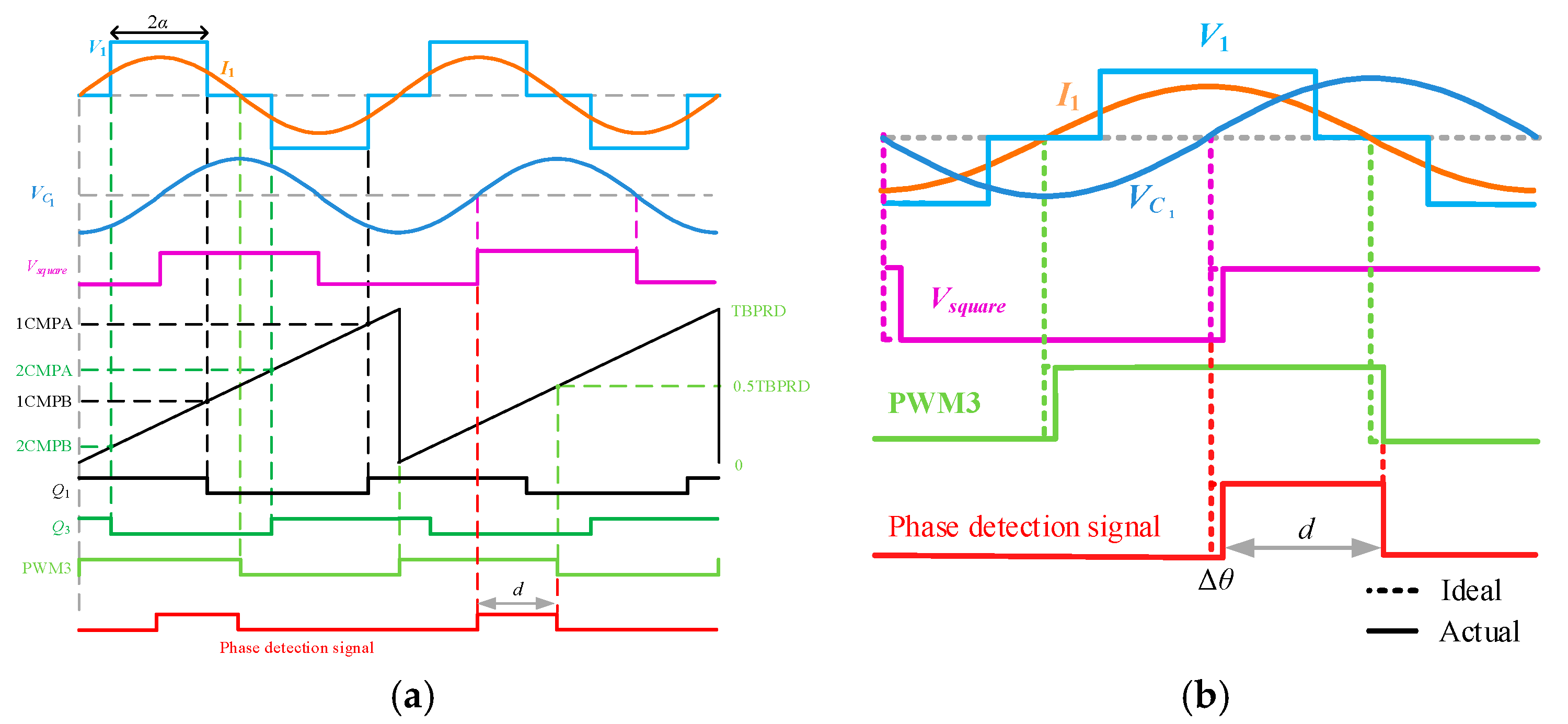
Since direct detection of high frequency PA is difficult, the phase information is modulated onto a DC voltage signal. The phase detection circuit is shown in Figure 7 and a graphical illustration in Figure 8a. CMPA and CMPB are the values of the reserved registers, and TBPRD is the time base period. The voltage across C1 () is divided by the resistors. Afterwards, the sinusoidal signal is sent to the comparator TLV3502-Q1 whose maximum operating frequency is 80 MHz. Then, a square wave is generated that goes through an isolator. PWM3 is controlled by the primary DSP. It is in phase with the fundamental voltage of V1, as shown in Figure 8a. The square wave Vsqaure and PWM3 pass through an AND gate, which can obtain a phase detection signal. Since I1 always leads by 90°, the pulse width of the phase detection signal d is:
The signal is sent to a single-pole/double-throw (SPDT) analog switch NC7SB3157 whose operating frequency can be as high as 250 MHz. Processed by a RC filter, the phase information is modulated onto the DC voltage Vphase. The voltage can be denoted as:
where Vcc is the power supply of the switch.
Then, θ can be calculated by:
In the unidirectional WPT system, θ ranges from −90° to 90°. Therefore, d ranges from 0 to 0.5. The voltage corresponding to 1° is . Since the valid sampling voltage of the selected DSP ranges from 0 to 3 V, the minimum voltage that can be distinguished is . Thus, the resolution of PA is:
Therefore, the theoretical accuracy can be 0.078° when Vcc is 3.3 V, which is acceptable for phase detection.
The main estimation error comes from two sources: the non-linearity of the analog chips and the time delay of the digital signal. The comparator turns the analog signal into a digital signal, whereas the analog switch turns it back. In order to improve the accuracy, high speed and high performance comparator and analog switch are chosen whose bandwidths are 800 and 2500 times greater than the operating frequency respectively, which will significantly reduce the influence of the non-linearity of the chips. The digital signal is insensitive to the noise, however, the time delay caused by the chips should be corrected as shown in Figure 8b. If PWM3 is generated without correction (as shown by the dashed line), an estimation error appears. This problem can be easily addressed by right shift of PWM3 via changing the corresponding register values. Since, the time delay is a constant value, a correction factor can be implemented. When V1 and I1 are in phase, after the regulation of PWM3, d should be 0.25, i.e., Vphase should be 0.25 Vcc.
The phase detection system shown in Figure 7 has several advantages likewise, the system can be easily corrected by PWM3 which can eliminate the influence of time delay, meanwhile the theoretical accuracy of the system is high. Secondly, is at high level and increases with the increase of transferred power, making it resilient to interference by switching noise. These characteristics contribute to an accurate detection of the point of zero-crossing. The robustness of the system should increase with the increase of the power level. Finally, it is based on the synchronization circuit that can be easily realized especially in the bidirectional WPT systems.
4.2. Synchronization
Although the transmitter and the receiver are isolated, they have rigorous time sequence. Therefore, synchronization is crucial. Different from previous works that use an additional measurement coil or a current sensor, this paper presents a novel method of using the voltage across C2 () for the synchronization, as shown in Figure 7. Since is at a higher level, it is not vulnerable to interference, ensuring the reliability of the synchronization circuit. At first, is divided across the resistors and a bidirectional Zener diode is paralleled to prevent overvoltage. Then, the divided sinusoidal voltage is sent to comparator TLV3502 and it can generate a square wave, indicating the zero-crossing point of . After passing through isolator ISO7710, this signal is sent to EPWM synchronization port (GPIO6 in TMS320F28335). The synchronization signal is only relative to the zero-crossing point of , hence this method can withstand large parameter variations including the operating frequency, the mutual inductance and the load. Since neither AMC nor the current sensor is used, this synchronization method is simpler and cheaper.
4.3. Additional Reactance and Mutual Inductance Estimations
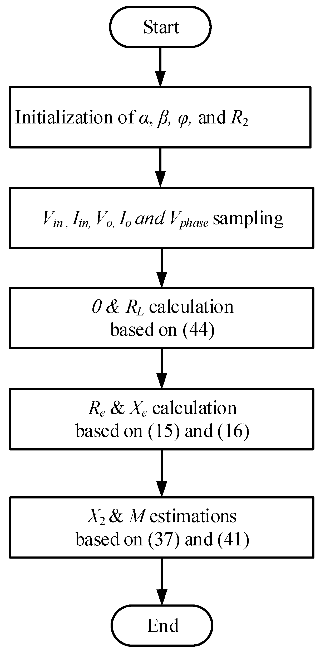
Additional reactance and mutual inductance can be estimated on-line according to the algorithm shown in Figure 9. The PAs are controlled, hence they are known in advance, as well as R2. Since Vin, Iin, Vo, Io and Vphase are DC signals, they can be sampled easily. RL is calculated by Vo/Io, and θ can be obtained according to (44). Then, Re and Xe can be calculated based on (15) and (16). Finally, additional reactance and mutual inductance estimations can be achieved according to Equations (37) and (41), respectively.
5. Simulation and Experimental Results
To verify the feasibility and effectiveness of the proposed system, a MATLAB/Simulink model and an experimental prototype are implemented. The system specifications are shown in Table 1. In addition, uncontrolled and synchronous rectifiers are added to compare with the proposed method. The synchronous rectification is a special case of PC, in which β = 90° and φ = 0°.
5.1. Simulation Results
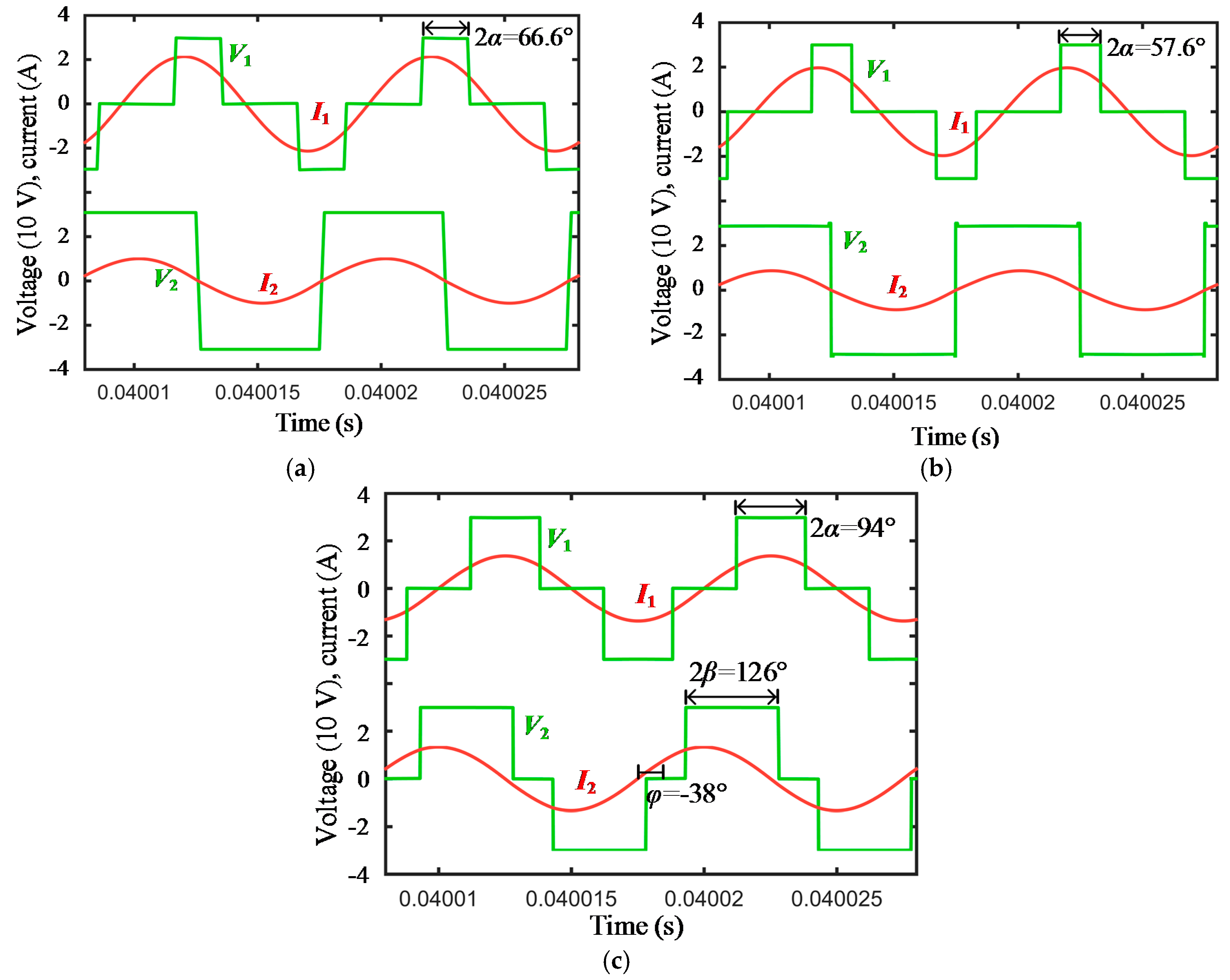
Figure 10 shows the simulated waveforms, where uncontrolled rectifier waveforms are shown in Figure 10a, synchronous rectifier waveforms in Figure 10b and MDPC waveforms in Figure 10c. C2 is 5.9 nF and RL is 50 Ω. To avoid the zero current crossing issue, the switches remain off and I2 flows through the diodes near zero current point. Thus, forward voltage of the diodes is added to V2. The output voltage stabilizes at the desired 30 V by regulating α. Although V2 and I2 are in phase both in Figure 10b, I1 leads V1. The equivalent impedance of uncontrolled and synchronous rectifiers are both resistive. However, additional inductive reactance exists on the secondary side, resulting in a reflected capacitive reactance on the primary side. Figure 10c shows the additional inductive reactance compensation results by MDPC. β and φ are set at 63° and −38° according to the calculations of Equations (29) and (30), whereas α is 47°. Since I2 leads V2, the equivalent impedance has capacitive and resistive components. The load is transformed to the optimal 20.1 Ω and the additional inductive reactance is compensated completely. Hence V1 is in phase with I1. Additional capacitive reactance can also be compensated as shown in Figure 4.
Although the above results prove that α can be used for voltage regulation, α is controlled to maintain a constant output power (18 W) for a more accurate efficiency comparison in the simulations and experiments.
C2 changes from 5.3 nF to 6.0 nF. The corresponding X2 ranges from −15 Ω to 20 Ω. Simulation results of α, β and φ versus X2 are shown in Figure 11. Although X2 varies, the transmitter sees it as the same due to compensation through MDPC. Thus, α almost remains unchanged. β and φ change with X2. The observed trends agree with the calculated results in Figure 6.
Figure 12a shows the simulation DC-DC efficiencies of load transformation where C2 is 5.6 nF. The equivalent impedances of the uncontrolled and synchronous rectifiers are resistive with a constant transformation ratio. Hence, uncontrolled and synchronous rectifiers just function as AC-DC converters. Although I2 decreases with the increase of the load, resulting in lower losses on the receiver side, I1 increases. Total losses caused by parasitic resistances increase when the load deviates from the optimal value. When the load varies in a large range, both the efficiencies of the uncontrolled and synchronous rectifier systems decrease significantly. However, the proposed MDPC method contributes to keeping the efficiency optimized. Since the load is transformed to the designed value, the influence of load mismatch is minimized. The uncontrolled rectifier system experiences the greatest efficiency drop due to the additional influence of the voltage loss in the diodes (1.6 V). For instance, if the transferred power is 18 W and the equivalent current flowing through two diodes is 0.67 A, the calculated efficiency drop will be 6%. Therefore, a large part of the transferred energy is consumed by the diodes.
Figure 12b shows the simulation DC-DC efficiencies of additional reactance compensation, where RL remains 50 Ω. The proposed system shows the lowest simulation efficiency of 93.9% during a large reactance variation. However, the lowest efficiencies of 87.5% and 71.6% are observed with the synchronous and uncontrolled rectifiers, respectively. Additional reactance is compensated by MDPC, hence the influence is eliminated. The existence of X2 requires higher input power, which degrades the efficiency as indicated by Equation (5). Thus, a larger |X2| results in a smaller overall efficiency in the uncontrolled and synchronous rectifier systems.
5.2. Experimental Results
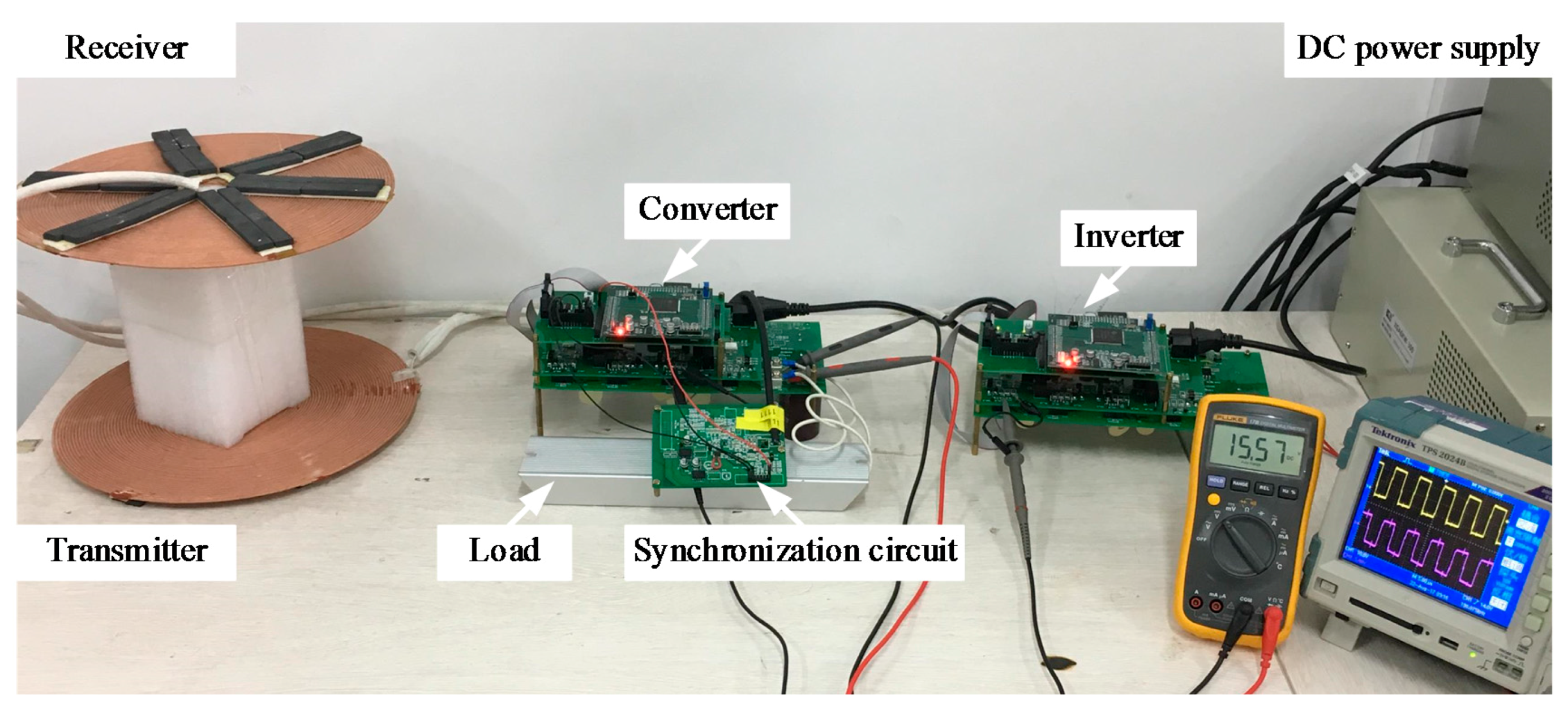
The photograph of the implemented prototype is shown in Figure 13. Primary active bridge inverts the DC voltage, thereafter, the power is transmitted through the coupling coils. Secondary active bridge converts the high frequency resonant current and the loading resistance consumes the energy. Synchronization circuit provides signal for the converter. Controllers on the primary and secondary sides generate a total of eight gate drive signals.
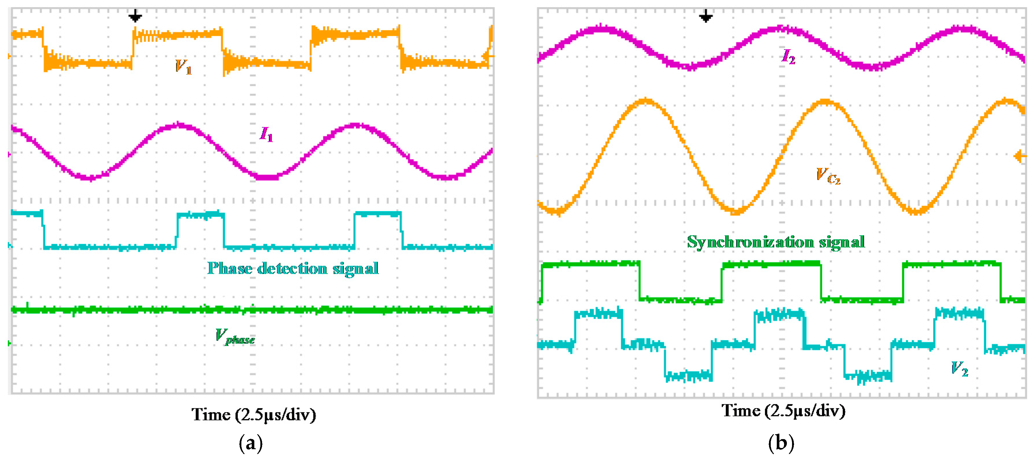
During initialization, a program for primary resonant frequency tracking is executed, with Vin being 2 V. The load is removed under this step and θ is detected. The operating frequency should increase for a positive θ, whereas decrease for a negative θ. f1 is locked when θ = 0, as shown in Figure 14a. Vphase should be 0.825 V theoretically.
Figure 14b shows the synchronization process. I2 flows through C2 and produces . The voltage is divided by the resistances and fed to a comparator, generating the synchronization signal. Afterwards, the secondary controller generates four gate drive signals based on it and then V2 is obtained. Figure 14c shows the estimated results of X2 and M. The estimated M is about 32 μH and X2 is about 10 Ω. Figure 15 shows the experimental waveforms when RL = 50 Ω. C2 is 5.9 nF in the first three experiments and 5.4 nF in the fourth experiment. Uncontrolled and synchronous rectifier waveforms are shown in Figure 15a,b, respectively. Additional inductive reactance exists on the receiver side, thus I1 leads V1. Only voltage regulation is obtained by the two methods. When uncontrolled rectification is applied, I2 and V2 are seen to be in phase in the simulation, whereas I2 leads V2 in the experimental results. V2 changes its state after I2 crosses zero point. The discharging and charging of the parasitic capacitors needs some time, resulting in a delay in V2. Although this phenomena can be reduced by using high performance diodes, an active rectifier used on the receiver side can address this problem completely. Additional inductive reactance compensation results is shown in Figure 15c. The additional inductive reactance is compensated, meanwhile load transformation and voltage regulation are achieved. It can be observed that I1 in Figure 15c is smaller than those in Figure 15a,b. With the same input voltage, lower input current implies lower input power and therefore, lower losses. Figure 15d shows the experimental results of additional capacitive reactance compensation. Although additional capacitive reactance exists, I1 is still in phase with V1 as expected.
The experimental results of α, β and φ vs. X2 are shown in Figure 16. α is higher than the simulation value due to the lower power transfer efficiency. The trends of β and φ agree with the simulation results.
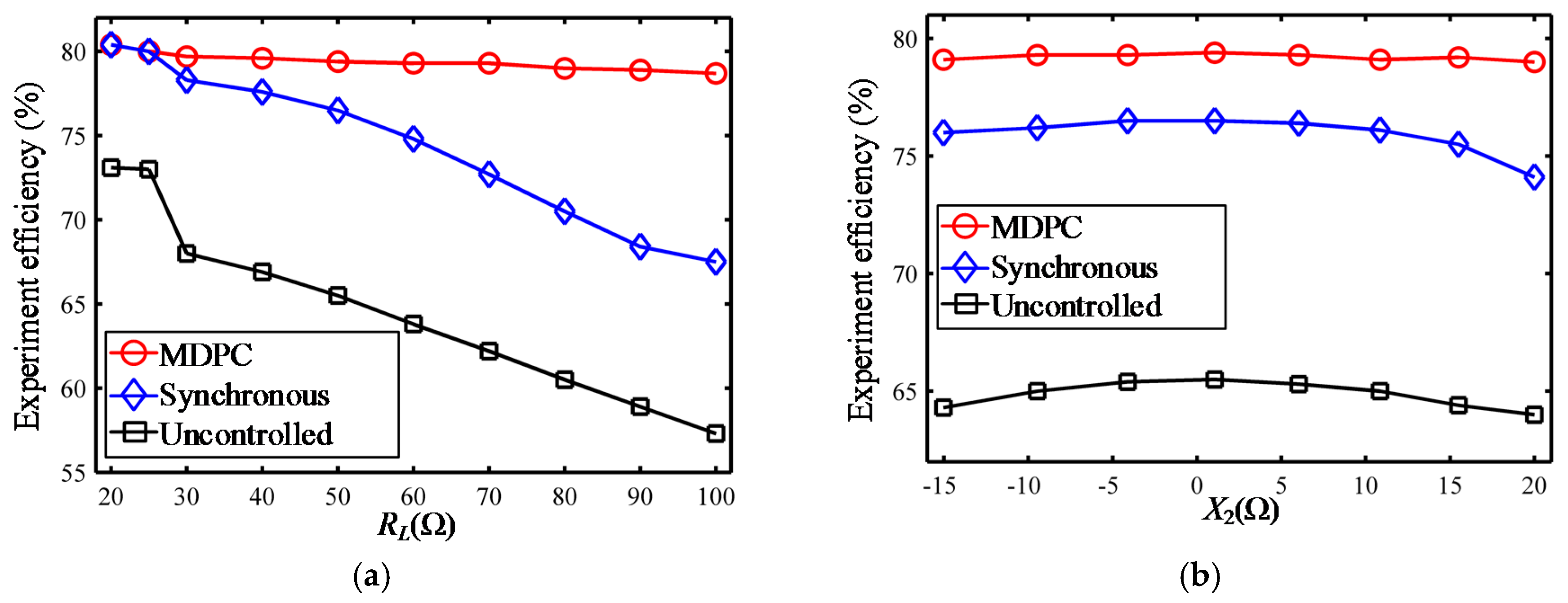
The DC-DC experimental efficiencies are summarized in Figure 17. Figure 17a illustrates the experimental DC-DC efficiencies versus the load when C2 = 5.6 nF. When RL approaches the optimal value 24.8 Ω, β is set at 90°. The synchronous rectifier system and the proposed method obtain the same overall efficiency of 80.4% with 21 cm distance between the transmitting and receiving coils. As RL deviates from the optimal value, the experimental efficiencies of the uncontrolled and synchronous rectifier systems decrease significantly, whereas the efficiency of the proposed system almost remains unchanged. Experimental results of additional reactance compensation are shown in Figure 17b, where RL is 50 Ω. The additional reactance requires higher apparent power and brings about efficiency degradation. Secondary PAs compensate the reactance and transforms the load simultaneously, thus the proposed system can attain higher efficiency than the other systems.
Switches, filtering capacitors, connecting wires and the surrounding components consume some energy. These additional losses take up a large proportion when the transferred power is low. Thus, an efficiency gap between the simulation results and experimental results are observed. Similar comparable gaps can be found in previous works. In [17], the power transfer efficiency is less than 65% when the transferred power is 100 W, whereas the overall efficiency is 92% with a 450-W load. An increase in the transferred power level can improve the overall system efficiency and gaps between the experimental result and simulations are reduced.
5.3. Discussion
DC-DC efficiencies from the simulations and experiments with the same system specifications are summarized in Table 2. The proposed MDPC system achieves the highest simulated efficiency of 94.1% and the highest experimental efficiency of 80.4%. The largest efficiency drops observed during large load and additional reactance variations are 0.6% for the simulation system and 1.7% for the experimental setup, respectively. In contrast, the other methods suffer from maximal 12.7% and 16.4% simulated and experimental efficiency drops, respectively. The proposed MDPC method can make full utilization of the three PAs for output regulation, reactance compensation and load transformation. It shows superiority to the other methods in terms of efficiency.
Secondary PC regulates equivalent resistance to obtain the optimal value and the extracted power remains almost unchanged. Therefore, primary PA requires few adjustments. This can mitigate the drawback of time delay in communication and benefits for dual-side regulation. In other words, only dual-side regulation can realize load transformation and output regulation simultaneously.
6. Conclusions
In this paper, the MDPC method in a SS WPT system is proposed, with which the voltage regulation, load transformation and additional reactance compensation are achieved simultaneously. The presented work addresses the problem of performance degradations caused by additional DC-DC converters, non-identical resonances and load mismatch, which increased the power transfer efficiency and insured a compact design. The additional reactance and mutual inductance estimation methods were realized based on DC information sampling. The phase detection method modulated phase information onto a DC voltage signal. In addition, a novel synchronization method consisting of a comparator and an isolator performed well at a frequency of 100 kHz. A simulated efficiency of 94.1% and an experimental efficiency of 80.4% were attained while delivering 18 W power with 21 cm distance between the transmitting and receiving coils.
Supplementary Materials
The following are available online at www.mdpi.com/1996-1073/10/10/1588/s1.
Acknowledgments
The authors acknowledge support from the National Natural Science Foundation of China grant 51277120 and United Foundation of NSFC-Henan grant U1604136.
Author Contributions
Xin Liu proposed the main idea, designed and performed the experiments, and wrote the manuscript. Tianfeng Wang, Xijun Yang and Nan Jin double-checked and discussed the results and the whole manuscript. Houjun Tang and Xijun Yang contributed to the discussion of this study. All authors have approved the final version of this manuscript.
Conflicts of Interest
The authors declare no conflict of interest.
References
- Kurs, A.; Karalis, A.; Moffatt, R.; Joannopoulos, J.D.; Fisher, P.; Soljacic, M. Wireless power transfer via strongly coupled magnetic resonances. Science 2007, 317, 83–86. [Google Scholar] [CrossRef] [PubMed]
- Sample, A.P.; Meyer, D.A.; Smith, J.R. Analysis, experimental results, and range adaptation of magnetically coupled resonators for wireless power transfer. IEEE Trans. Ind. Electron. 2011, 58, 544–554. [Google Scholar] [CrossRef]
- Lu, Y.; Ma, D.B. Wireless Power Transfer System Architectures for Portable or Implantable Applications. Energies 2016, 9, 1087. [Google Scholar] [CrossRef]
- Wang, Z.; Wei, X.; Dai, H. Design and Control of a 3 kW Wireless Power Transfer System for Electric Vehicles. Energies 2016, 9, 10. [Google Scholar] [CrossRef]
- Lee, S.-H.; Kim, J.-H.; Lee, J.-H. Development of a 60 kHz, 180 kW, Over 85% Efficiency Inductive Power Transfer System for a Tram. Energies 2016, 9, 1075. [Google Scholar] [CrossRef]
- Bashirullah, R. Wireless implants. IEEE Microw. Mag. 2010, 11, S14–S23. [Google Scholar] [CrossRef]
- Wei, X.; Wang, Z.; Dai, H. A Critical Review of Wireless Power Transfer via Strongly Coupled Magnetic Resonances. Energies 2014, 7, 4316–4341. [Google Scholar] [CrossRef]
- Kim, J.; Kim, J.; Kong, S.; Kim, H.; Suh, I.-S.; Suh, N.P.; Cho, D.-H.; Kim, J.; Ahn, S. Coil design and shielding methods for a magnetic resonant wireless power transfer system. Proc. IEEE 2013, 101, 1332–1342. [Google Scholar] [CrossRef]
- Zhong, W.X.; Hui, S.Y.R. Maximum energy efficiency tracking for wireless power transfer systems. IEEE Trans. Power Electron. 2015, 30, 4025–4034. [Google Scholar] [CrossRef]
- Hu, P.; Ren, J.; Li, W. Frequency-Splitting-Free Synchronous Tuning of Close-Coupling Self-Oscillating Wireless Power Transfer. Energies 2016, 9, 491. [Google Scholar] [CrossRef]
- Mai, R.; Ma, L.; Liu, Y.; Yue, P.; Cao, G.; He, Z. A Maximum Efficiency Point Tracking Control Scheme Based on Different Cross Coupling of Dual-Receiver Inductive Power Transfer System. Energies 2017, 10, 217. [Google Scholar] [CrossRef]
- Fu, M.; Yin, H.; Zhu, X.; Ma, C. Analysis and tracking of optimal load in wireless power transfer systems. IEEE Trans. Power Electron. 2015, 30, 3952–3963. [Google Scholar] [CrossRef]
- Ahn, D.; Hong, S. Wireless power transfer resonance coupling amplification by load-modulation switching controller. IEEE Trans. Ind. Electron. 2015, 62, 898–909. [Google Scholar] [CrossRef]
- Berger, A.; Agostinelli, M.; Vesti, S.; Oliver, J.A.; Cobos, J.A.; Huemer, M. A Wireless Charging System Applying Phase-Shift and Amplitude Control to Maximize Efficiency and Extractable Power. IEEE Trans. Power Electron. 2015, 30, 6338–6348. [Google Scholar] [CrossRef]
- Li, H.; Li, J.; Wang, K.; Chen, W.; Yang, X. A maximum efficiency point tracking control scheme for wireless power transfer systems using magnetic resonant coupling. IEEE Trans. Power Electron. 2015, 30, 3998–4008. [Google Scholar] [CrossRef]
- Diekhans, T.; De Doncker, R.W. A dual-side controlled inductive power transfer system optimized for large coupling factor variations and partial load. IEEE Trans. Power Electron. 2015, 30, 6320–6328. [Google Scholar] [CrossRef]
- Bac, X.N.; Vilathgamuwa, D.M.; Foo, G.H.B.; Wang, P.; Ong, A.; Madawala, U.K.; Trong, D.N. An EfficiencyOptimization Scheme for Bidirectional Inductive Power Transfer Systems. IEEE Trans. Power Electron. 2015, 30, 6310–6319. [Google Scholar]
- Thrimawithana, D.J.; Madawala, U.K.; Neath, M. A Synchronization Technique for Bidirectional IPT Systems. IEEE Trans. Ind. Electron. 2013, 60, 301–309. [Google Scholar] [CrossRef]
- Madawala, U.K.; Thrimawithana, D.J. A Bidirectional Inductive Power Interface for Electric Vehicles in V2G Systems. IEEE Trans. Ind. Electron. 2011, 58, 4789–4796. [Google Scholar] [CrossRef]
- Colak, K.; Asa, E.; Bojarski, M.; Czarkowski, D.; Onar, O.C. A Novel Phase-Shift Control of Semibridgeless Active Rectifier for Wireless Power Transfer. IEEE Trans. Power Electron. 2015, 30, 6288–6297. [Google Scholar] [CrossRef]
- Mai, R.; Liu, Y.; Li, Y.; Yue, P.; Cao, G.; He, Z. An Active Rectifier Based Maximum Efficiency Tracking Method Using an Additional Measurement Coil for Wireless Power Transfer. IEEE Trans. Power Electron. 2017, 99, 1. [Google Scholar] [CrossRef]
- Kobayashi, D.; Imura, T.; Hori, Y. Real-time coupling coefficient estimation and maximum efficiency control on dynamic wireless power transfer for electric vehicles. In Proceedings of the IEEE PELS Workshop Emerging Technologies: Wireless Power, Daejeon, Korea, 5–6 June 2015. [Google Scholar]
- Yin, J.; Lin, D.; Parisini, T.; Hui, S.Y. Front-End Monitoring of the Mutual Inductance and Load Resistance in a Series–Series Compensated Wireless Power Transfer System. IEEE Trans. Power. Electron. 2016, 31, 7339–7352. [Google Scholar] [CrossRef]
- Li, Y.; Mai, R.; Lin, T.; Sun, H.; He, Z. A Novel WPT System Based on Dual Transmitters and Dual Receivers for High Power Applications: Analysis, Design and Implementation. Energies 2017, 10, 174. [Google Scholar] [CrossRef]
- Thrimawithana, D.J.; Madawala, U.K.; Yu, S. Design of a bi-directional inverter for a wireless V2G system. In Proceedings of the IEEE International Conference on Sustainable Energy Technologies (ICSET), Kandy, Sri Lanka, 6–9 December 2010; pp. 1–5. [Google Scholar]
Figure 1.
Proposed multiple degrees of phase control in a WPT system: (a) schematic of the proposed system; (b) equivalent circuit of the proposed system.
Figure 1.
Proposed multiple degrees of phase control in a WPT system: (a) schematic of the proposed system; (b) equivalent circuit of the proposed system.
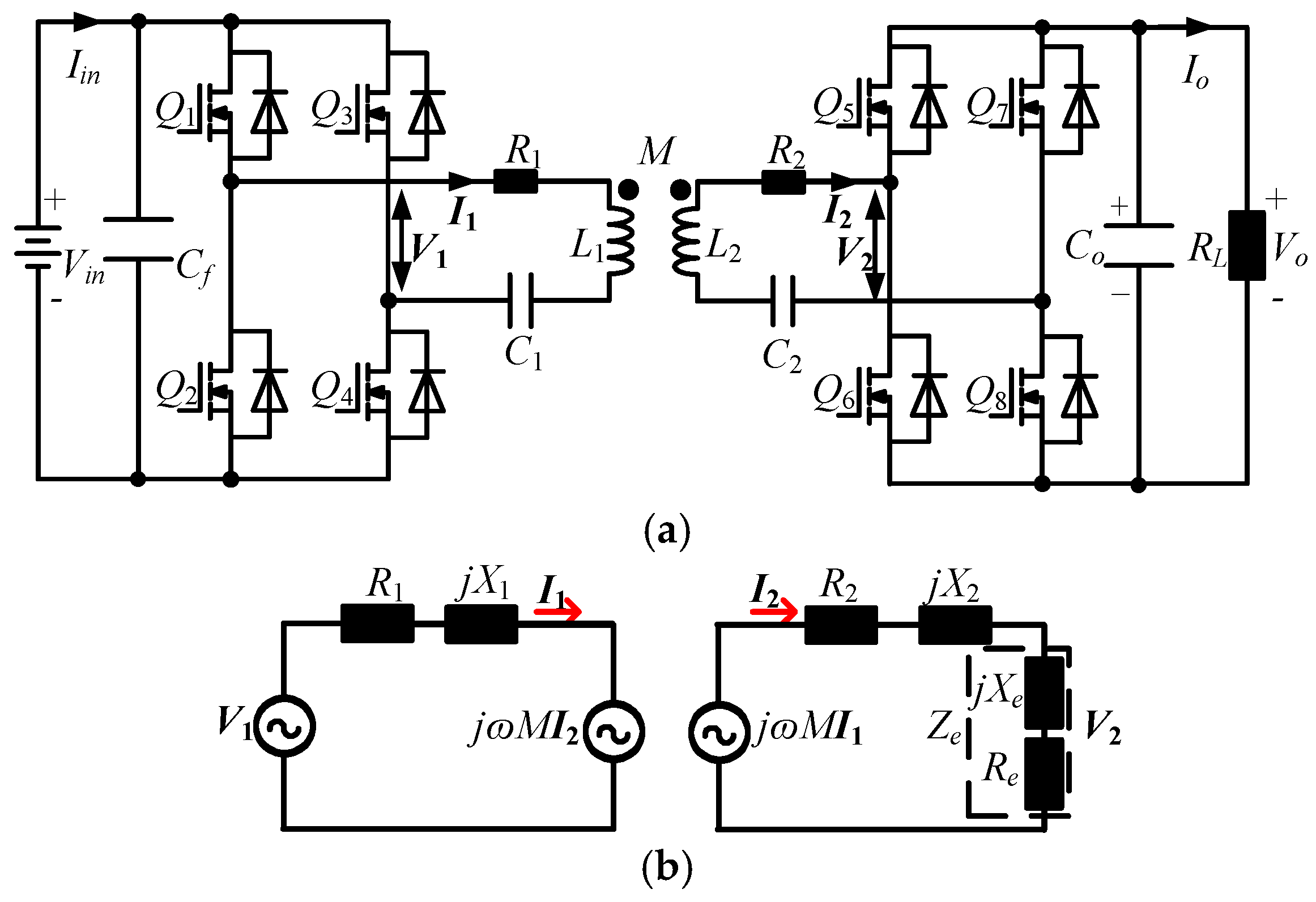
Figure 2.
Three dimensional plot of the power transfer efficiency η versus the load RL and the additional reactance X2.
Figure 2.
Three dimensional plot of the power transfer efficiency η versus the load RL and the additional reactance X2.
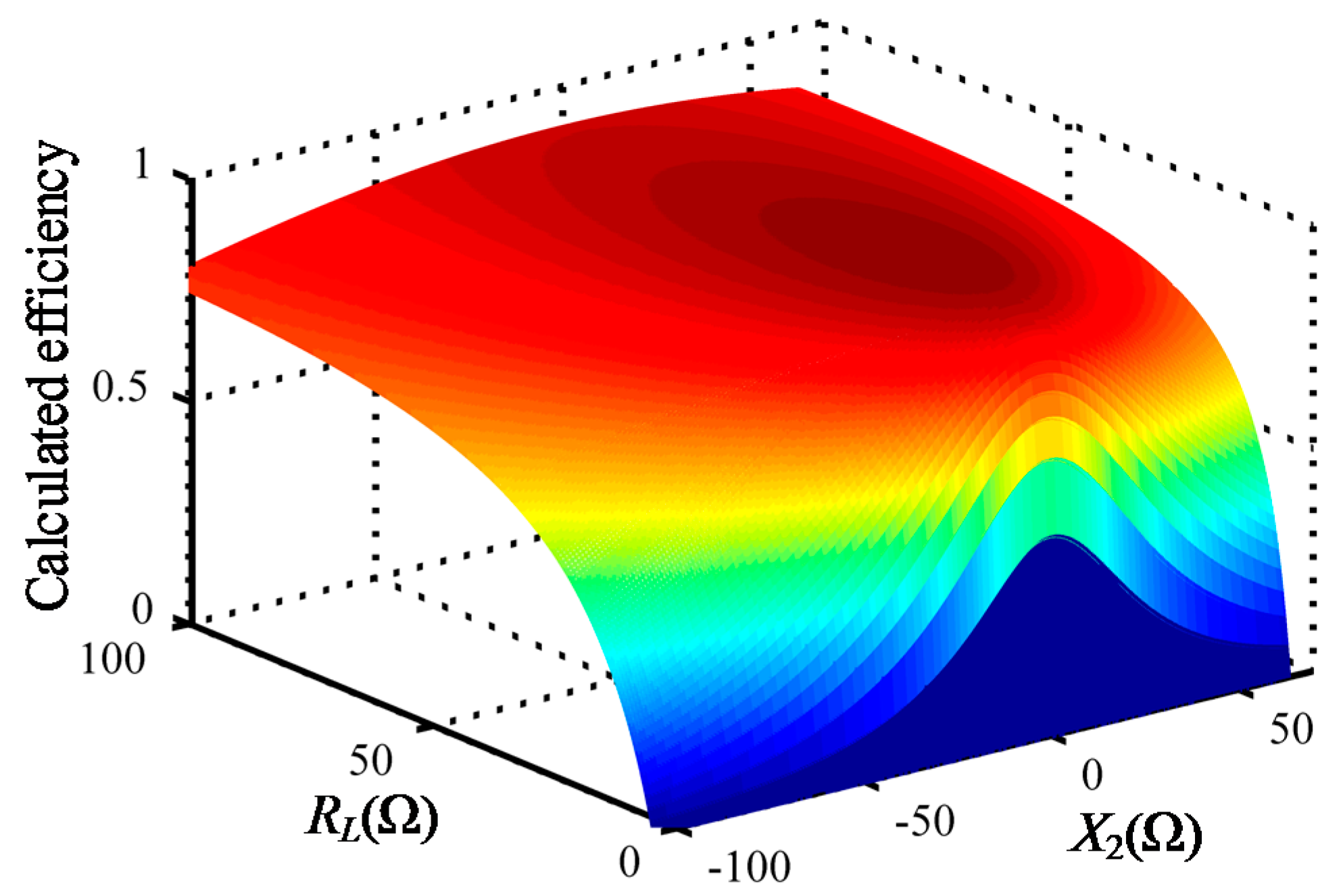
Figure 3.
Square-wave voltages (black lines), fundamental voltages (blue dashed lines) and resonant currents (orange lines) in a SS WPT system: (a) primary active bridge; (b) secondary active bridge.
Figure 3.
Square-wave voltages (black lines), fundamental voltages (blue dashed lines) and resonant currents (orange lines) in a SS WPT system: (a) primary active bridge; (b) secondary active bridge.

Figure 4.
Simulated waveforms of the proposed MDPC.

Figure 5.
Load transformation ratio m and reactance compensation ratio n versus φ and β: (a) load transformation ratio; (b) reactance compensation ratio.
Figure 5.
Load transformation ratio m and reactance compensation ratio n versus φ and β: (a) load transformation ratio; (b) reactance compensation ratio.
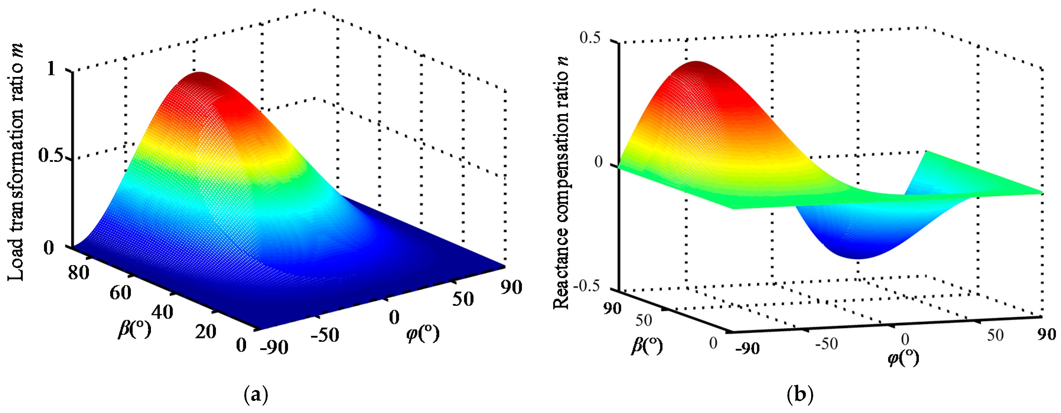
Figure 6.
Optimal phase angles φ and β versus the additional reactance X2.
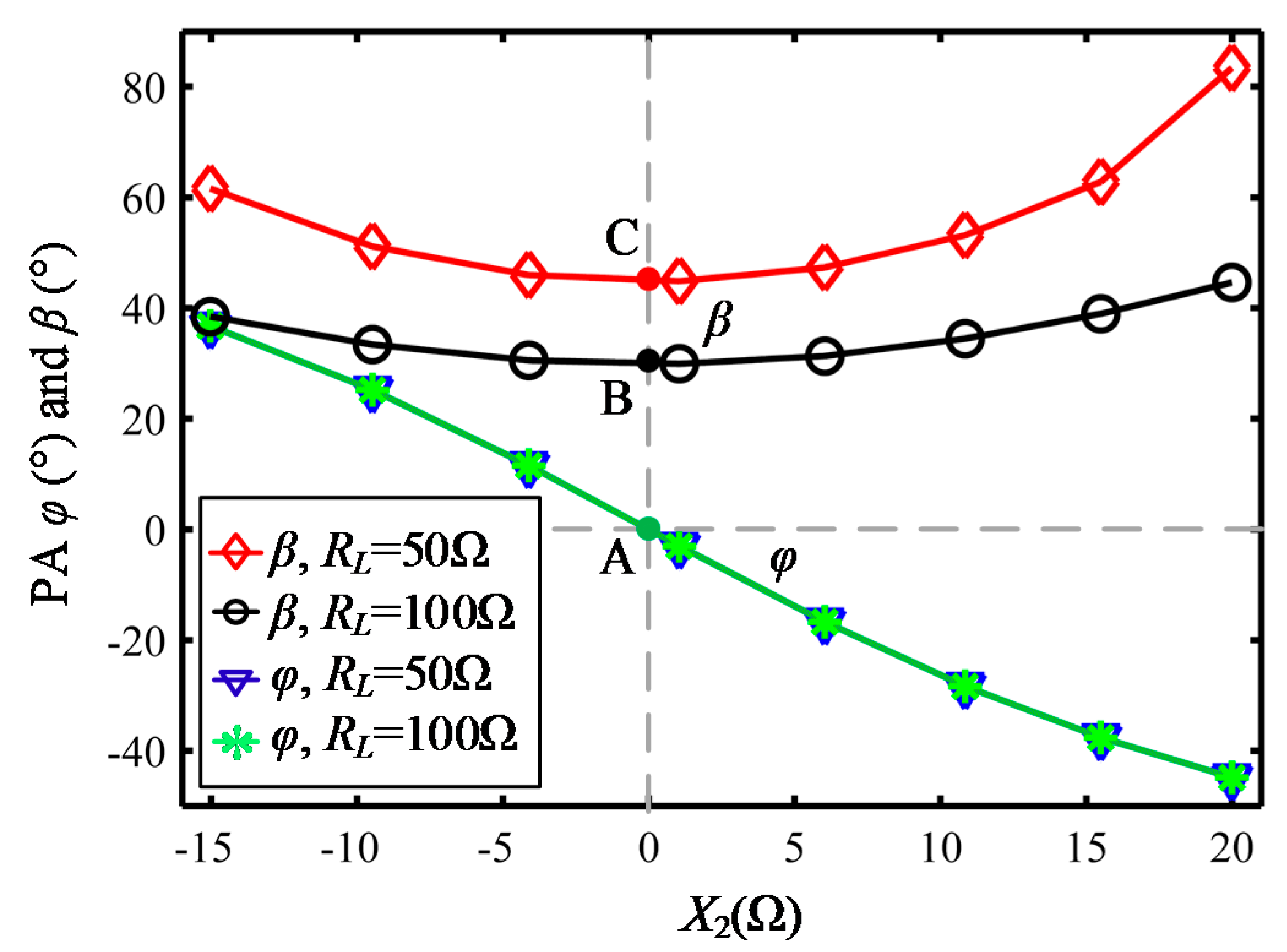
Figure 7.
Overall system block diagram.

Figure 8.
Generation of phase detection signal: (a) graphical illustration; (b) time delay elimination.
Figure 8.
Generation of phase detection signal: (a) graphical illustration; (b) time delay elimination.

Figure 9.
Flowchart of parameter estimation program.

Figure 10.
Simulated waveforms: (a) uncontrolled rectifier; (b) synchronous rectifier; (c) additional inductive reactance compensation and load transformation by proposed MDPC.
Figure 10.
Simulated waveforms: (a) uncontrolled rectifier; (b) synchronous rectifier; (c) additional inductive reactance compensation and load transformation by proposed MDPC.

Figure 11.
Simulation phase angles vs. additional reactance under MDPC.
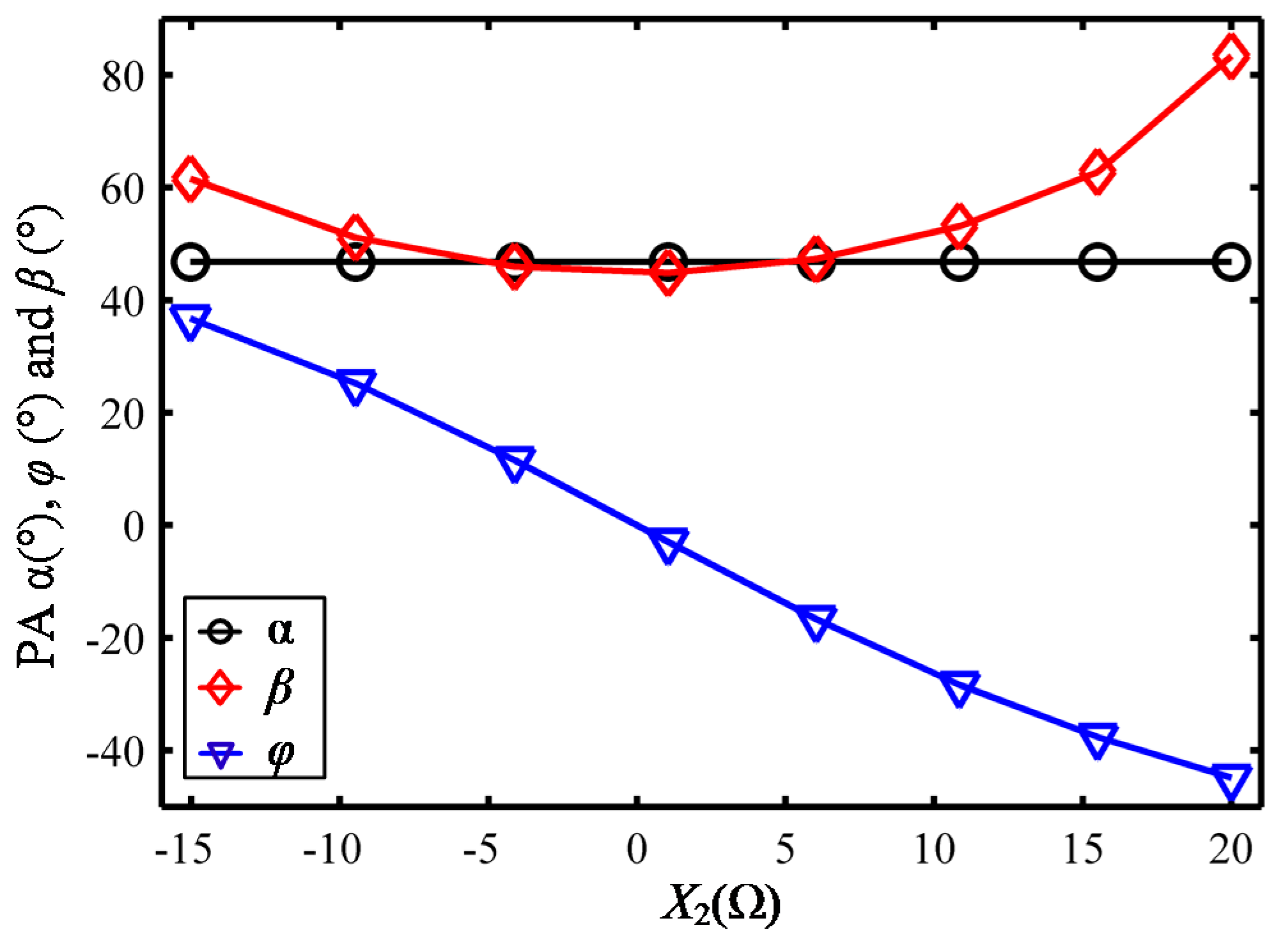
Figure 12.
Simulation efficiency comparison of different methods: (a) simulation efficiency vs. load; (b) simulation efficiency vs. additional reactance.
Figure 12.
Simulation efficiency comparison of different methods: (a) simulation efficiency vs. load; (b) simulation efficiency vs. additional reactance.
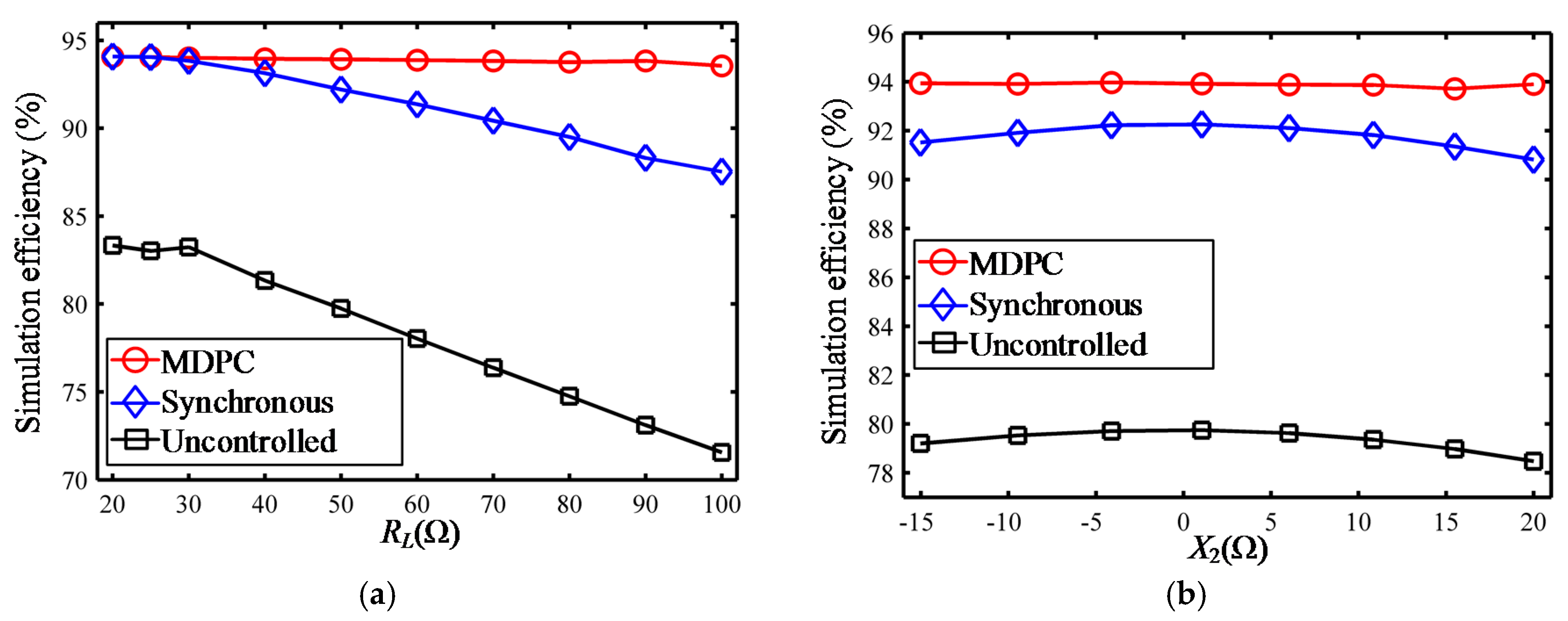
Figure 13.
Photograph of the prototype.

Figure 14.
Experimental results: (a) phase detection; (b) synchronization; (c) additional reactance and mutual inductance estimations.
Figure 14.
Experimental results: (a) phase detection; (b) synchronization; (c) additional reactance and mutual inductance estimations.

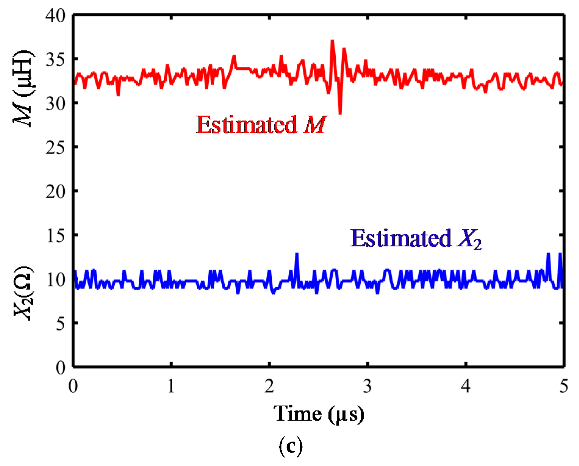
Figure 15.
Experimental waveforms: (a) uncontrolled rectifier; (b) synchronous rectifier; (c) additional inductive reactance compensation and load transformation by MDPC; (d) additional capacitive reactance compensation and load transformation by MDPC.
Figure 15.
Experimental waveforms: (a) uncontrolled rectifier; (b) synchronous rectifier; (c) additional inductive reactance compensation and load transformation by MDPC; (d) additional capacitive reactance compensation and load transformation by MDPC.
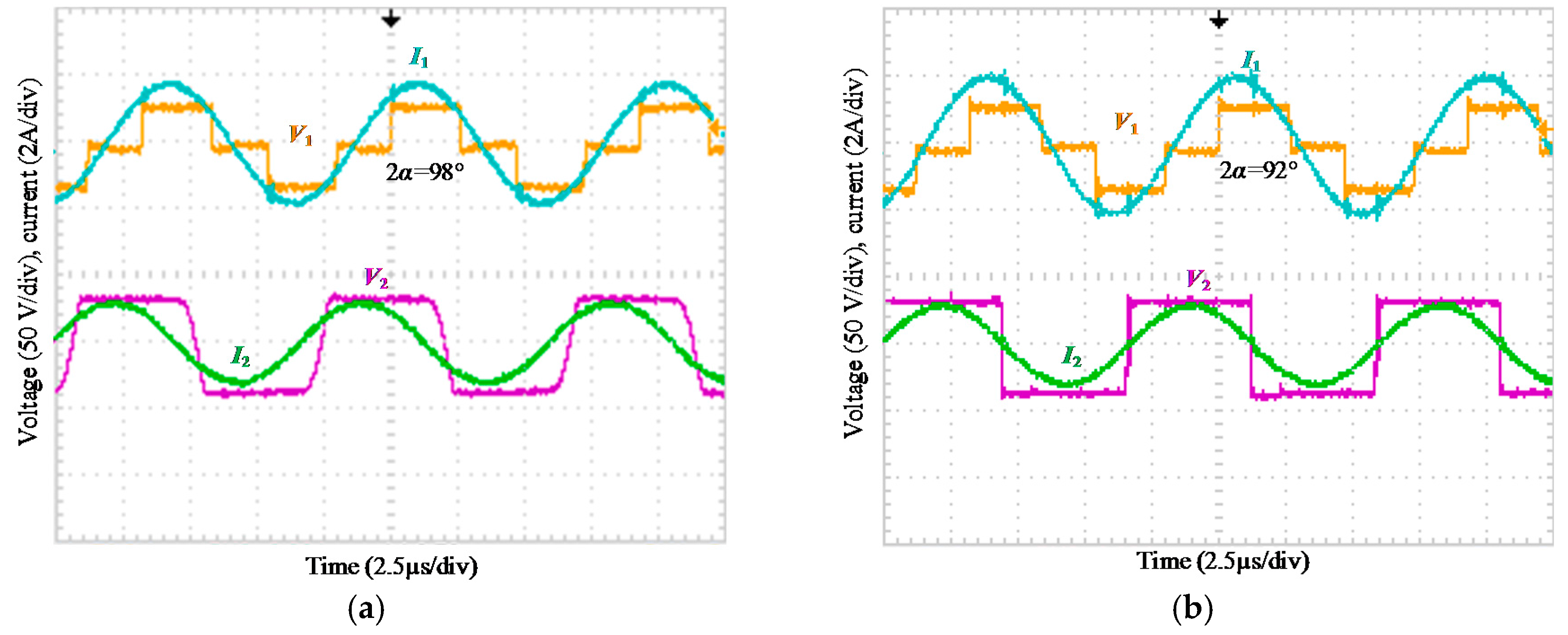
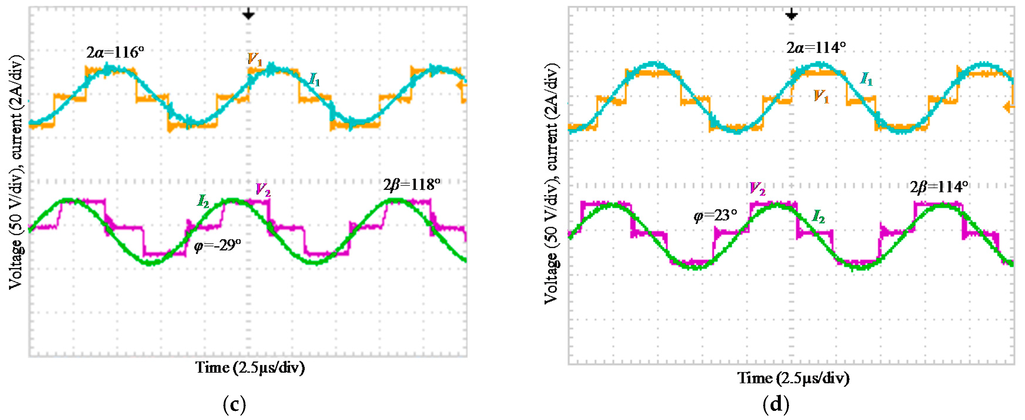
Figure 16.
Experimental results of PAs versus additional reactance under MDPC.
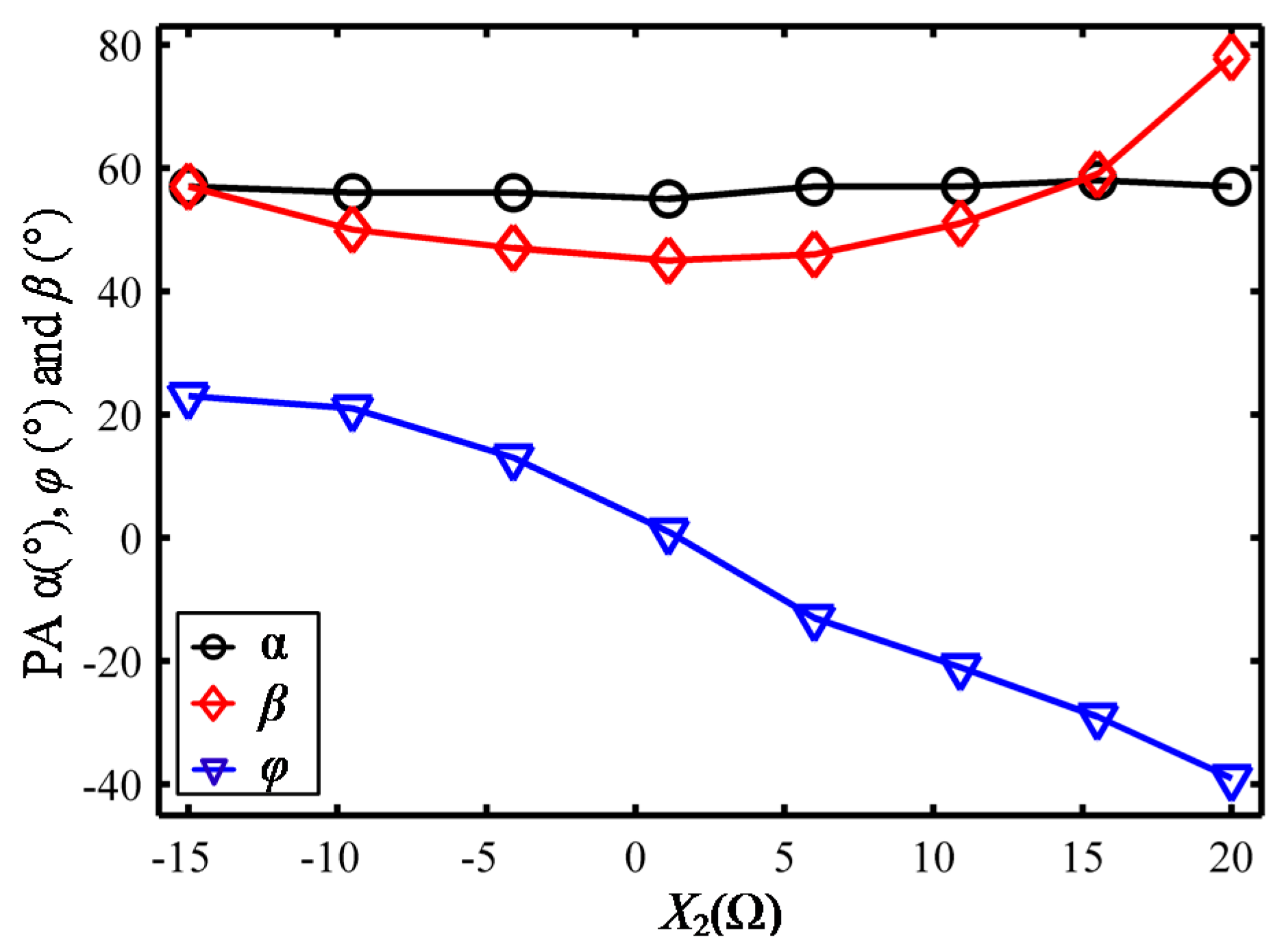
Figure 17.
Experimental efficiency comparison of different methods: (a) experimental efficiency versus load; (b) experimental efficiency versus additional reactance.
Figure 17.
Experimental efficiency comparison of different methods: (a) experimental efficiency versus load; (b) experimental efficiency versus additional reactance.


Table 1.
Key parameters of the proposed system.
| Symbol | Quantity | Value |
|---|---|---|
| L1, L2 | inductances of transmitting and receiving coils | 475 μH, 454 μH |
| C1 | primary compensation capacitor | 5.3 nF |
| C2 | secondary compensation capacitor | [5.3, 6.0] nF |
| R1, R2 | parasitic resistances | 0.5 Ω, 0.5 Ω |
| f | operating frequency | 100 kHz |
| M | mutual inductance | 32 μH |
| RL | loading resistance | [20, 100] Ω |
| Vin | input voltage | 30 V |
Table 2.
DC-DC efficiencies of simulations and experiments.
| Header | Uncontrolled Rectifier | Synchronous Rectifier | MDPC |
|---|---|---|---|
| Maximum simulated efficiency (%) | 83.3 | 94.1 | 94.1 |
| Minimum simulated efficiency (%) | 71.6 | 87.5 | 93.5 |
| Simulated efficiency drops (%) | 12.7 | 6.6 | 0.6 |
| Maximum experimental efficiency (%) | 73.1 | 80.4 | 80.4 |
| Minimum experimental efficiency (%) | 57.3 | 64 | 78.7 |
| Experimental efficiency drops (%) | 15.8 | 16.4 | 1.7 |
© 2017 by the authors. Licensee MDPI, Basel, Switzerland. This article is an open access article distributed under the terms and conditions of the Creative Commons Attribution (CC BY) license (http://creativecommons.org/licenses/by/4.0/).
Share and Cite
MDPI and ACS Style
Liu, X.; Wang, T.; Yang, X.; Jin, N.; Tang, H. Analysis and Design of a Wireless Power Transfer System with Dual Active Bridges. Energies 2017, 10, 1588. https://doi.org/10.3390/en10101588
AMA Style
Liu X, Wang T, Yang X, Jin N, Tang H. Analysis and Design of a Wireless Power Transfer System with Dual Active Bridges. Energies. 2017; 10(10):1588. https://doi.org/10.3390/en10101588
Chicago/Turabian StyleLiu, Xin, Tianfeng Wang, Xijun Yang, Nan Jin, and Houjun Tang. 2017. "Analysis and Design of a Wireless Power Transfer System with Dual Active Bridges" Energies 10, no. 10: 1588. https://doi.org/10.3390/en10101588
Note that from the first issue of 2016, this journal uses article numbers instead of page numbers. See further details here.