1. Introduction
In shipboard power systems, space limitations make direct current (DC) a favorable option, as compared to alternating current (AC), as this can lead to reduction in cable size for the same power level [
1,
2]. This downsizing is envisioned not just in the cable’s conductor size, but also in the insulation requirements. For land-based distribution grids, refurbished operation of underground AC cables under DC can deliver power more efficiently and at higher transfer capacity for the same thermal constraints, while avoiding extra investment in digging and infrastructure installation [
3]. Furthermore, in urban areas, need for compact power redirection with emerging energy intensive distributed resources is driving the necessity of medium voltage (MV) DC distribution.
For these applications, an underlying assumption is that as compared to AC, a higher DC voltage can be imposed on the insulation [
4,
5,
6]. Applying this principle, it was shown in [
7] that, even with a conservative DC voltage enhancement factor of
times the r.m.s 50 Hz AC voltage, a capacity gain of at least 50% could be achieved. However, a definitive proof of this assumption and its impact on cable insulation life is still missing in the literature. The goal of this research is to contribute to developing the empirical knowledge on the insulation performance in order to validate the feasibility of such anticipated gains of DC versus AC, and determining the comparative impact of different operational conditions from a component engineering point of view. The technique chosen for determining insulation performance is the measurement of partial discharge activity within the cable, with a specific focus on voids at semicon-dielectric interfaces.
1.1. Background on Partial Discharges in Insulation Systems
Solid insulation systems typically consist of dielectric materials of sufficiently high breakdown strengths bridging the gap between the high and low voltage electrodes. Their function is to provide mechanical support to the electrodes while withstanding electric and thermal stresses for long durations of time, sometimes on the order of tens of years as is the case with underground cable systems. Tiny voids present within the dielectric, as well as at electrode–insulation interface have much lower breakdown strengths, leading to partial discharges (PD) within these voids [
8]. The detrimental effect of PDs resulting in material degradation due to modification in its chemical composition and its eventual complete breakdown has been discussed in [
9]. In [
10], it is mentioned that the rate of deterioration is expected to be greater for voids adjacent to the electrode, as compared to those completely enclosed within the dielectric. Therefore, this study concentrates on voids existing at semiconducting (semicon)-dielectric interface.
Two important parameters of PD behavior governing the lifetime performance of the insulation are the repetition rate (
), measured in number of discharge pulses per second, and discharge magnitude (
), usually measured in pico-Coulomb (pC). Deterioration depends on both
and
, but in different ways.
increases with applied voltage and frequency of operation [
11,
12]. The probable role of applied frequency, electric field and
in governing the deterioration limit is highlighted in [
10,
11]. Defining this limit as a certain discharge magnitude below which deterioration is negligible, these papers specify that it is not a sharp limit. Discussing how the void diameter has little effect on the rate of deterioration after a certain threshold, it was shown how discharges concentrate in deep un-carbonized pits of smaller diameter within the void [
10]. Nevertheless, it can be inferred that the role of
and
in governing the insulation lifetime is intrinsically related.
Knowledge on the mechanism of void PD behavior and factors influencing its inception voltage, recurrence and evolution in time is necessary. A good discussion on these aspects is provided in [
13,
14,
15]. Some aspects relevant in supporting our observations are discussed here.
1.1.1. PD Initiation
The two necessary conditions for a PD event are: (1) voltage across the void is greater than its breakdown strength; and (2) availability of free electrons to initiate the discharge.
The first condition determines the partial discharge inception voltage (PDIV), which is defined as the voltage above which discharge occurs, and depends on the kind of gas in the void, its pressure and the void dimensions. The breakdown phenomenon in an insulation void is consistent with the Paschen’s curve [
16]. The PDIV is usually 10–20% lower than the breakdown voltage obtained from the Pashcen’s curve [
17]. It follows that, under the conditions of this experiment, the PDIV is possibly independent of frequency of applied voltage, a trend we observed under specific conditions in this work. This behavior was also reported previously in [
18]. However, the presence of space charges and trapped surface charges may distort the field across the defect and may result in higher observed PDIV, particularly under DC conditions.
The second necessary condition implies that there is a finite time lag
after reaching PDIV, but before a discharge is initiated. This time lag in availability of electrons to initiate a discharge is stochastic, resulting in a statistical over-voltage
V [
19]. It was shown that the
is proportional to
V [
14], which, in turn, affects the residual voltage across the void after the discharge has occurred.
Physical location and dimensions of the void in the insulation system are also important. For example, a flat void perpendicular to the field can have a field enhancement by the dielectric relative permittivity
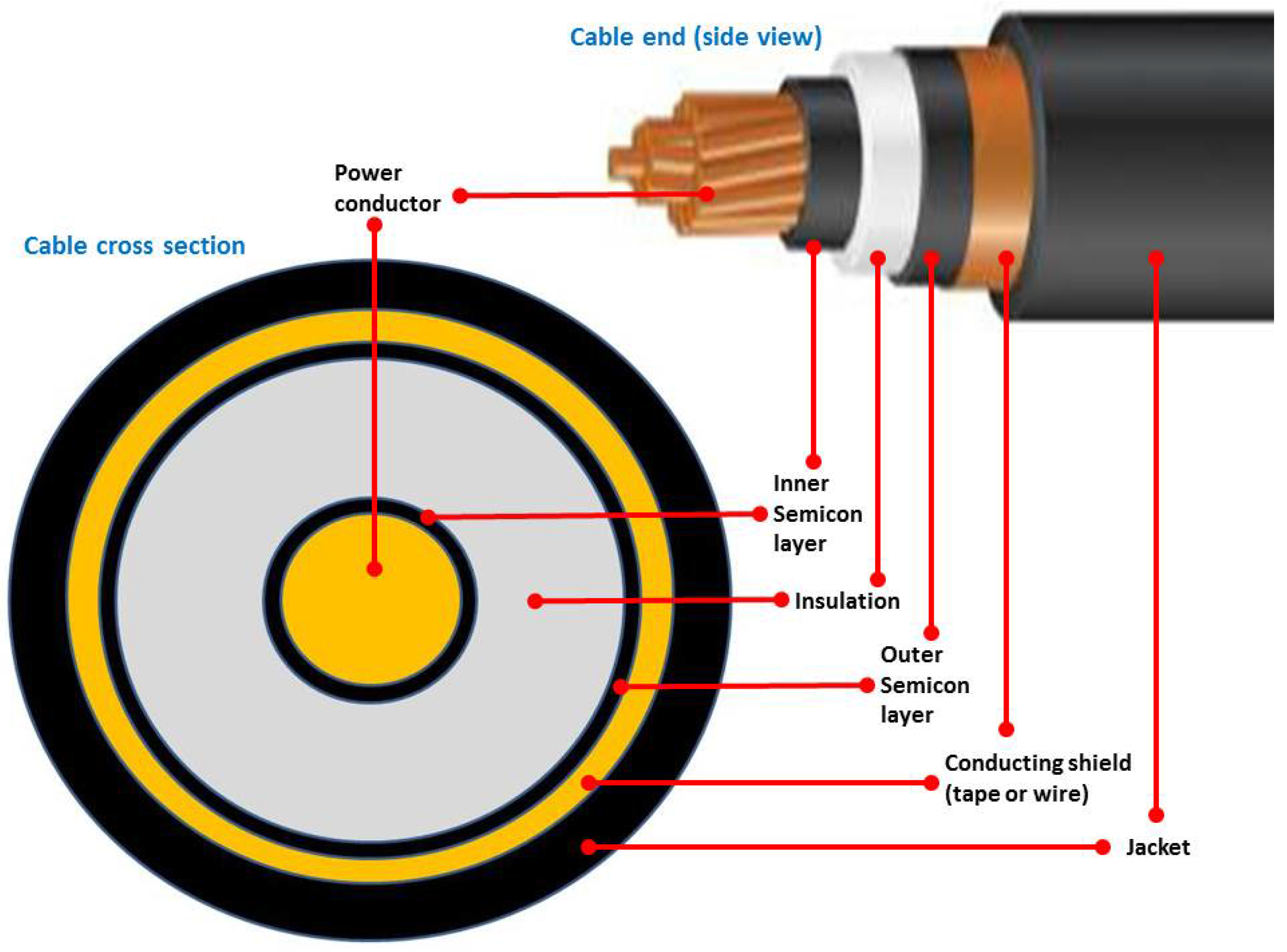
. The location may cause asymmetry in electric field, causing different discharge patterns with positive and negative polarities. However, most importantly, experimental data suggests that the material acting instantaneously as the cathode influences the discharge behavior. For example, the void can be between the inner semicon layer, which is in direct contact with the inner conductor and the insulation that surrounds it, or between the insulation and the outer semicon layer, which is in direct contact with the outer shield (
Figure 1). In the first instance, assuming that the central conductor is at a positive voltage and the outer shield is grounded, the insulator wall would act as the cathode, whereas, in the second instance, it would be the anode. This role will reverse when the central conductor is at negative polarity. Based on the availability of free electrons, it is discussed in [
20] how there is a greater tendency of discharges when the insulation wall acts as the cathode. On the other hand, the discharge magnitude is greater when the semicon wall in the void is negative [
17]. However, unlike the observations in [
17,
20], the findings of [
21] suggested that negative PDs have higher
as compared to positive PDs. The defects studied in the same reference were of different type at the termination of the MV High-density Cross-linked Polyethylene (XLPE) cable, but still involved the outer semicon layer and the insulation.
1.1.2. Recurrence
The recurrence of PD after a discharge event depends on the recovery time
during, which the voltage across the void builds from the residual voltage to its inception and the statistical lag time. The combined effect of these two ultimately determines the PD repetition rate and discharge magnitude. The relationships are illustrated in Equations (
1) and (
2):
It is discussed how
is inversely proportional to
V [
22] which is independent of the applied voltage (
) [
14,
19]. These two relationships are illustrated in Equations (
3) and (
4):
Equation (
3) tells us that the statistical nature of time lag implies a spread in
V and ,therefore, the observable
. Physically, Equation (
3) intuits that a higher
V decreases the expected statistical time lag [
22], implying that this distribution in
will favour lower discharge magnitudes if all the other variables are constant. Equation (
4) mandates that, with increasing applied voltage,
must be decreasing if
V is to be constant [
19]. This in combination with Equation (
1) implies that
may increase with applied voltage. On the other hand,
depends inversely on the charge decay rate
, which is a function of void dimensions (area
A, diameter
d), conductivity (
) and the average electric field (
) [
23] as illustrated in Equation (
5):
This means that
will decrease with increase in
d,
and
, while increase with corresponding increase in
A. This has implications on
according to Equation (
1).
1.1.3. Void Evolution
Erosion and chemical degradation caused by the PDs lead to a gradual deterioration of the dielectric, which, in turn, changes the behavior of the PD [
18]. This is important to take into account while empirically analyzing the data. We observed in our preliminary results that fundamental frequency AC quickly altered the test artificial void. Therefore, in order to minimize the detrimental effect of PDs while studying the trends, a frequency range of 0–0.1 Hz and an applied voltage range of 0–20 kV was used.
On the other hand, the way the void evolves as well as its subsequent effect on insulation performance is important to determine insulation life. For an ageing void at the metal–insulation interface, it was observed in Ref. [
24] that the PD repetition rate decreases in time, accompanied with higher
and increasing PDIV. The same reference shows how trace conductor material from the copper electrode migrates towards the dielectric due to PD activity and ionized air particles. In [
25], it is predicted based on the conductivity change due to the migration of metallic material towards the insulation layer that space charges may appear, thus decreasing the electric field under DC conditions. It would be interesting to explore whether the test samples used in this study exhibit the aforementioned behavior and determine some empirical understanding about its trend with the considered operating conditions, but this information is yet unavailable as of this writing.
1.1.4. PD Behaviour with AC versus DC Applied Voltage
It has been suggested that the PD rate in cable insulation with DC operation is lower than AC under similar conditions [
15,
26]. This is because the DC time constant
determined from the cable insulation parameters governs the PD
. It was discussed in Ref. [
15] that, unlike the case of commercial 50–60 Hz AC, where the
influences the repetition rate,
is orders of magnitude higher than the theoretical value that would give equivalent PD
. This relationship is illustrated in Equation (
6), derivation for which is shown in Ref. [
15]:
Our initial tests on artificially created voids embedded within insulation of Ethylene Propylene Rubber (EPR) and XLPE MV (5–30 kV) cables showed that DC voltage enhancement of at least five times could still give significantly lower PD
. The insulation performance over its lifetime also depends on the PDIV. Furthermore, under DC voltage, space charges are able to develop when there is conductivity gradient in the dielectric (due to thermal gradient, electrode migration or carbonization), leading to field distortion and lowering of PD activity if polarity reversal is avoided. A good theoretical discussion on space charges relevant to the conditions of our study is provided in Ref. [
25]. A broader perspective on the role of space charges in bringing the insulation to failure is offered in Ref. [
27]. Another reason may be that, since steady-state DC electric field is governed by the conductivity of the materials, the field strength in the void is much less than that in dielectric, which may result in less PDs under DC voltage.
1.2. Research Focus
The focus of our paper is to develop empirical knowledge on PD behavior in a void at the semicon-dielectric interface of a medium voltage EPR power cable. The inferences derived from our observations will be supported by the principles discussed in
Section 1.1. Measured trends at medium voltage levels (0–20 kV) and low frequency (0.01–0.1 Hz) will be analyzed as compared to DC. Change in discharge activity with void evolution will be studied in order to gather understanding on the operational practices under DC that would at least maintain the same expected insulation performance as in the case of AC.
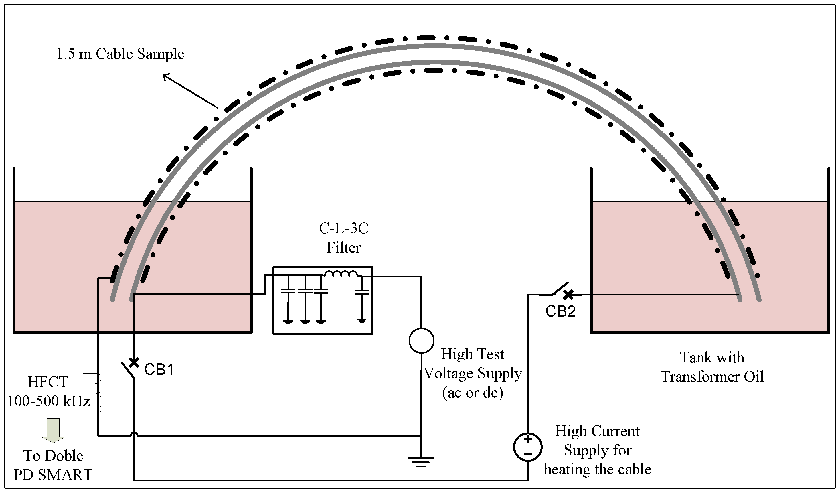
2. Experimental Setup and Test Procedure
The schematic of the test setup is shown in
Figure 2.
Cable samples of 1.5 m were used and the layers at the termination at both ends were cut in a graded manner to ensure uniformly varying stress. These cable terminations were immersed in transformer oil to minimize partial discharges at these locations [
28]. The C-L-3C filter, with
C = 2 nF and
L = 40 mH arranged in a configuration as shown in
Figure 2, has increasing attenuation greater than −6 dB above 10 kHz, thus filtering noise from the high voltage (HV) supply. The HV inductor of the filter is also completely submerged in the oil.
The high frequency current transformer (HFCT) was used to capture the small signals generated by the PD in the cable dielectric. The connection was such that a positive PD was recorded when the polarity of the inner conductor was positive. All the power equipment was reliably grounded for safe and accurate PD measurement. The data were processed by the IEC 60270 compliant [
29] PD Smart system manufactured by Doble (Watertown, MA, USA) with a band-pass of 100–500 kHz and transferred to a computer for visualization. Unless otherwise mentioned, the threshold for PD measurement was set at 10 pC.
A high current DC power supply capable of providing up to 600 A was used to heat the cable sample. Isolators CB1 and CB2 (shown in
Figure 2) were installed to manually disconnect the high current supply during HV tests. Simultaneous operation of a high current and HV supply was avoided as this operation posed safety concerns. Furthermore, the 600 A DC source created significant radiated noise, which obfuscated the measurement from the HFCT. To hold the test sample temperature at the desired value during HV tests, the oil in the tanks at both ends could also be heated up to 80
C using immersion heating rods. The mathematical basis and experimental validation of this method is presented in [
30]. Since the present paper only reports data at room temperature, the high current set-up was used only to thermally age the cable and the oil heating apparatus was not used.
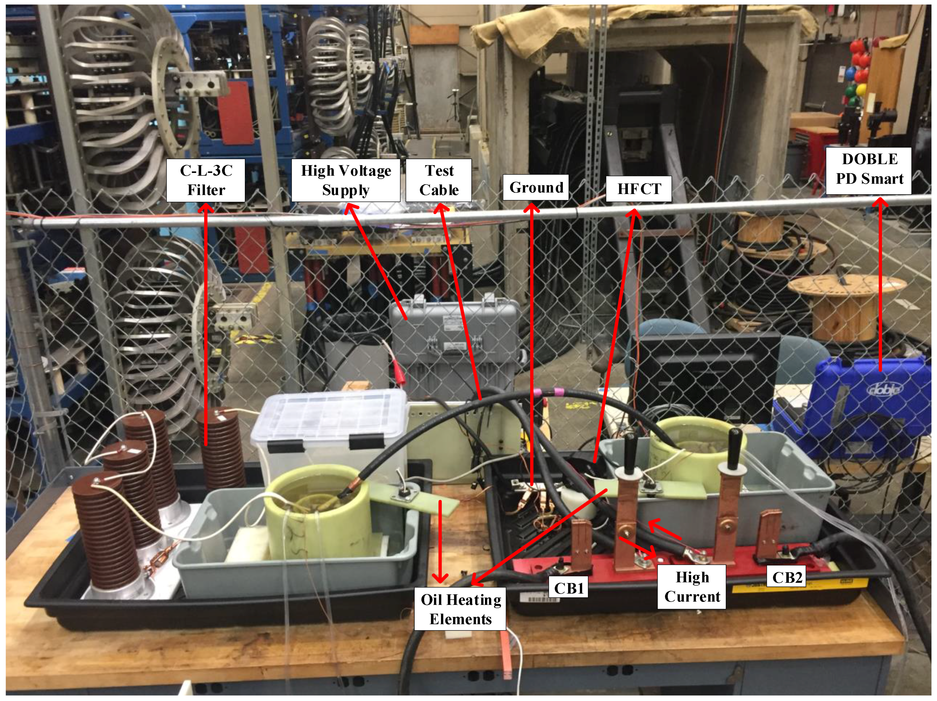
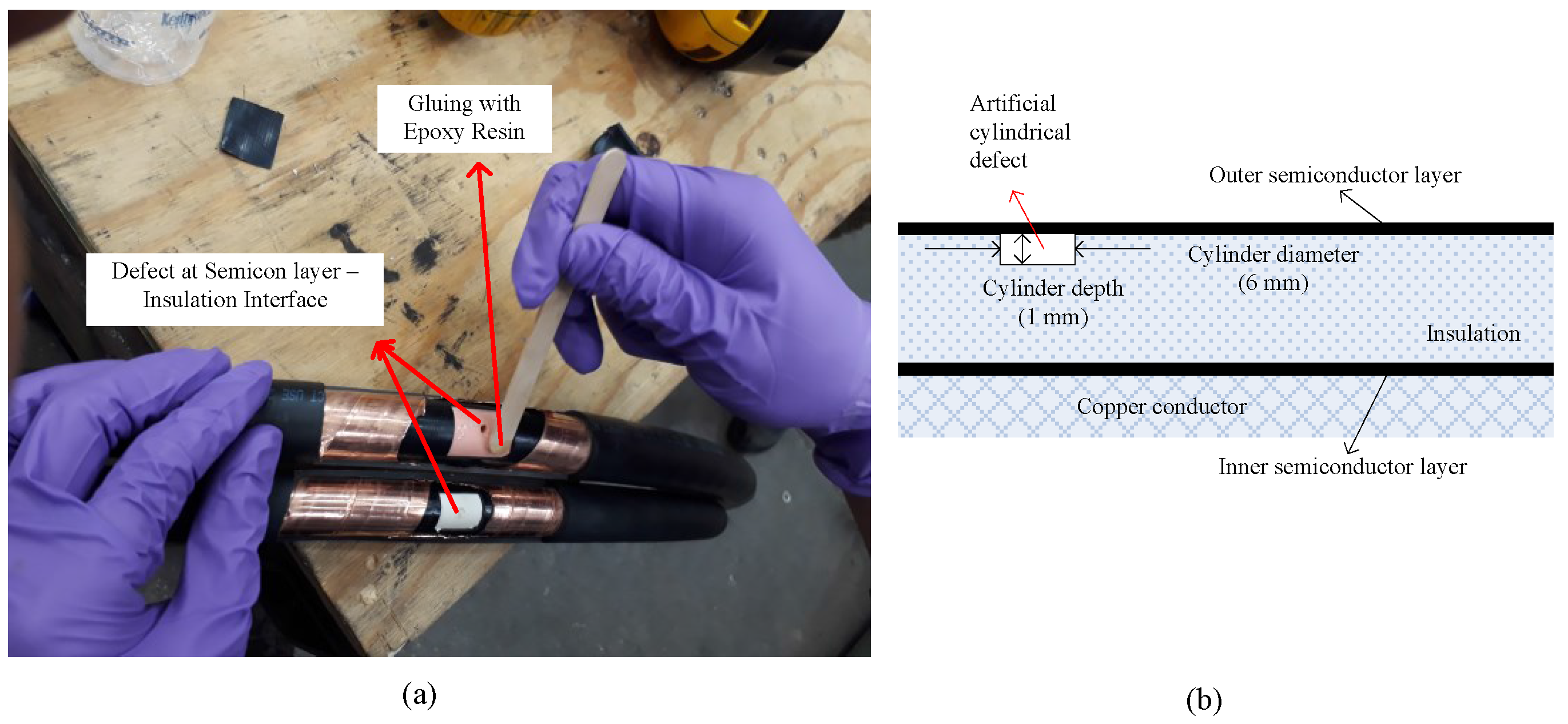
The physical realization of the experimental setup at the test site is shown in
Figure 3. The setup includes an HV power supply (either AC or DC), a C-L-3C filter, test cable, HFCT, and PD measurement equipment (Doble PD Smart).
Figure 4 shows a snapshot of two test cables being prepared with artificial defects in the insulation at its interface with the outer semicon-layer. The location of the artificial void of 1 mm depth and 6 mm diameter in the cable at the interface of the outer semicon-layer and the insulation is shown. The dimensions of the void were chosen to achieve clear differentiation between PD activity and noise. A good discussion on the PD activity with different void dimensions is provided in Ref. [
23]. Note that this insight is offered for artificial voids completely encompassed by the insulation.
The rectangular segments of the outer layer, metallic shield and the semicon layer are carefully removed one by one without damaging the outer surface of the cable insulation. Then, an artificial defect of the desired dimensions can be drilled. The bottom surface of the defect is made to be as smooth as possible. The image shows how the Epoxy resin is applied at the surface around the defects to firmly fix the semicon-layer. Finally, the metallic shield and the outer protective sheath are reattached to obtain the test cable samples.
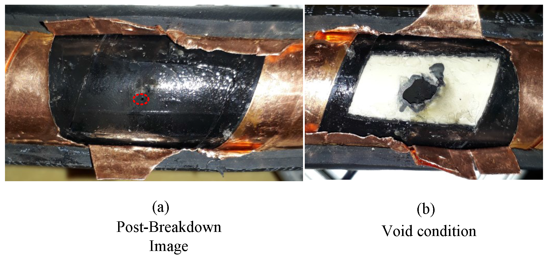
The snapshots of a test cable post breakdown is shown in
Figure 5.
In
Figure 5a, the post breakdown semicon layer segment above the artificial defect is shown. A pinhole developed in this damaged layer is highlighted. After reopening the semicon layer,
Figure 5b shows the carbonized insulation layer. These images provide physical evidence of significant discharge activity at the defect location. The analysis results presented in this paper are from a different cable sample with identical specifications, void dimensions and preparation procedure.
A healthy undamaged cable was tested under similar conditions in the set-up and no discharge activity was measured in this configuration. This observation, together with the physical evidence of localized post-breakdown at the artificial defect, increased confidence that the measurement results offered in this paper are partial discharges in the insulation layer void created at its interface with the semicon layer.
In addition, testing was performed to determine if the process of preparing the artificial void resulted in unintended excessive PD activity. For this purpose, the procedure described by
Figure 4a was followed without creating the artificial void in a separate cable sample of identical specifications. In other words, the semicon layer was removed and re-fixed similar to the test sample without drilling the void. The altered cable was then tested in the same ranges of frequencies and applied voltages. Measurement results for PD repetition rate of defect cable as compared to the one without defect is shown in
Table 1.
It can be observed that, even at the highest test voltage level of 20 kV, the total PD activity is significantly lower in the cable in which no defect is present even though the semicon layer had been previously removed and replaced. Furthermore, the values reported in
Table 1 for the altered cable were predominantly out of phase with the applied voltage, a condition that indicates that the source of the measured PD activity was located outside the cable (this point will be discussed in more detail later). In conclusion, the confidence level that the PD activity measured in the cable with a void defect does indeed result from the void itself is very high.
3. DC Voltage Enhancement Ratio with Respect to the Fundamental AC
The preliminary results of this section were presented in [
31]. A 5 kV EPR cable (5 kV 133% insulation Cu EPR cable) with an artificial defect was used. The defect was a cylindrical void of 6 mm diameter and 1 mm depth. It was created at the interface of the inner semicon layer and insulation.
This is considered to be the worst case scenario as the void is not internal to the insulation [
10]. Furthermore, the location is such that the void experiences the maximum electric field. In the first test, the cable was tested under 60 Hz AC voltage. In the second test, the same sample was tested under DC voltage. The operating condition was at ambient room temperature and pressure. The voltage was slowly raised until the PDIV and the PD was measured from HFCT installed around the ground return from the cable shield using a PD Smart meter. The connection was made such that a positive PD corresponded to a positive cycle of the applied voltage.
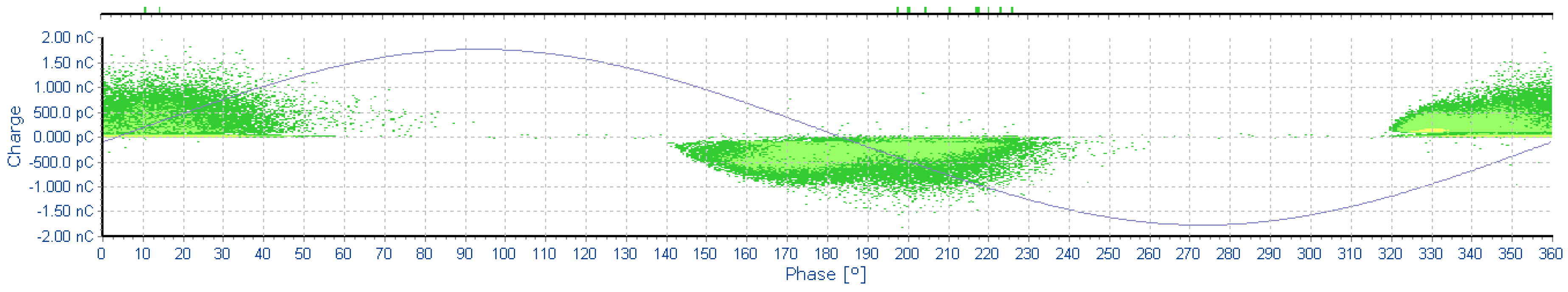
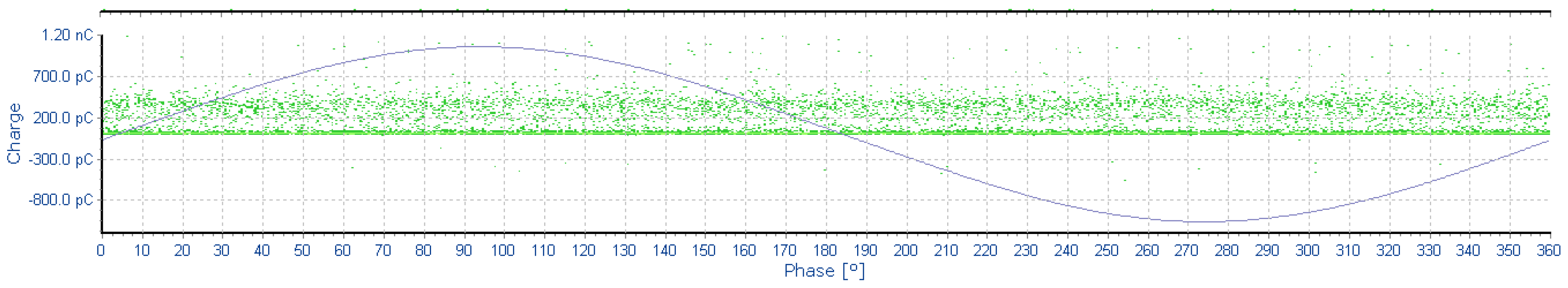
The pattern diagrams for partial discharges measured at 4.5 kV rms 60 Hz AC and 6.6 kV DC are shown in
Figure 6 and
Figure 7, respectively. Note that the internal meter voltage reference shown in the figures is delayed with respect to the actual imposed AC voltage by 130 degrees: this must be considered in evaluating the expected phase angle at which the discharges are observed in
Figure 6.
In the DC case at 6.6 kV, which was the PDIV, the repetition rate was sporadic at ≈5 pulses per second. In the AC case, the repetition rate was much higher at 200 per second at 4.5 kV rms 60 Hz voltage (with a peak voltage of 6.4 kV). The PDIV for 60 Hz AC was 3.5 kV rms (almost 5 kV peak) at which the repetition rate was 5–70 pulses per second with an average of pulses 20 pulses per second. The maximum discharge magnitude was the same (≈2 nC) for both AC and DC and the PD activity was audible.
When the cable was retested under 60 Hz AC sine wave, the PDIV had increased from 3.5 kV to 4 kV rms, at which the rate was two pulses per second. Furthermore, at 4.5 kV rms, the rate had decreased from 200 pulses per second to 100–120 pulses per second. This behavior could possibly indicate the change in conductivity in the vicinity of the void.
Under repeated DC testing, no PD activity was observed until 7.2 kV. At 7.8 kV DC, PD activity was observed, but immediately there was significant audible PD activity near the void location and, shortly thereafter, the HV DC supply tripped, indicating complete breakdown of the cable.
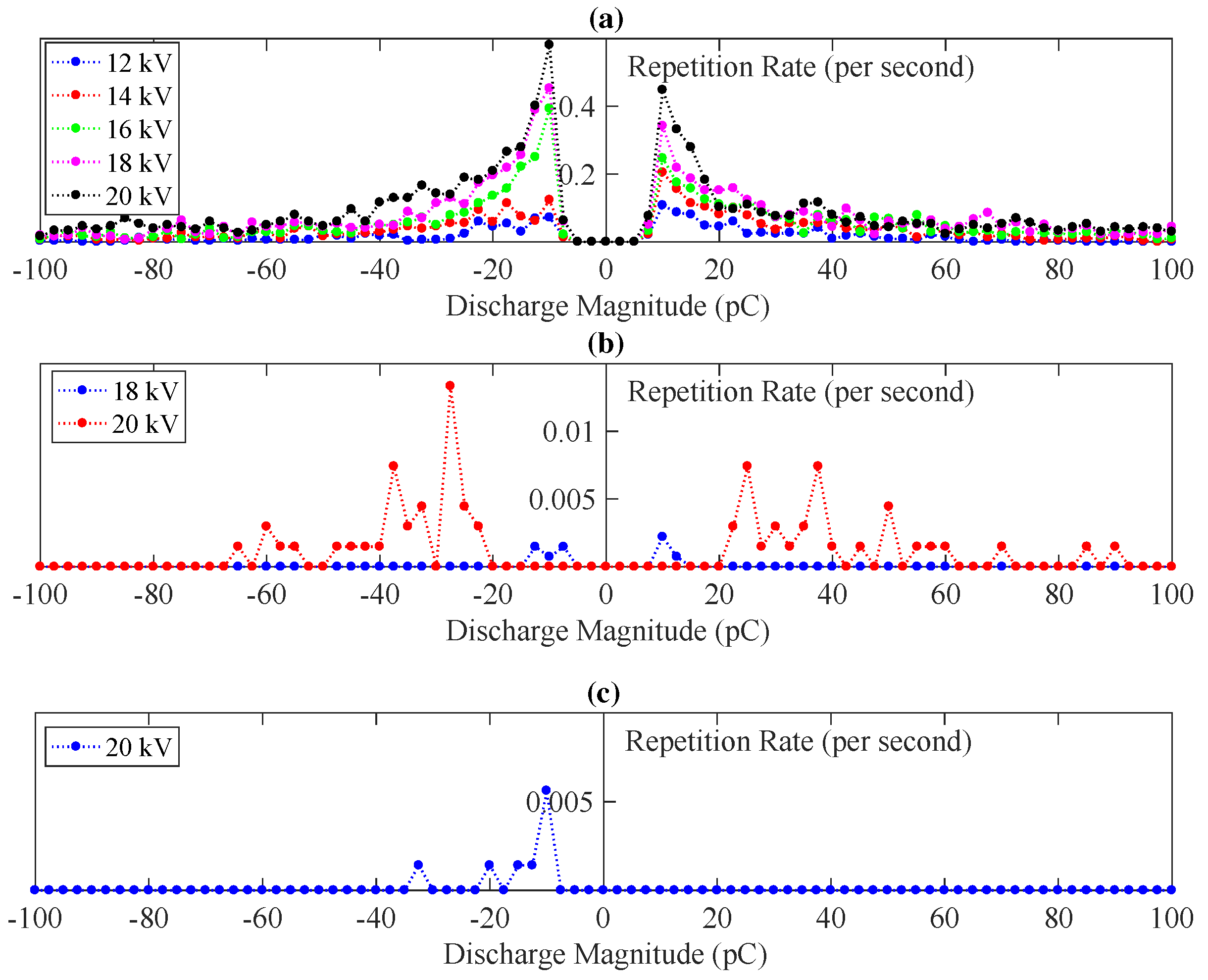
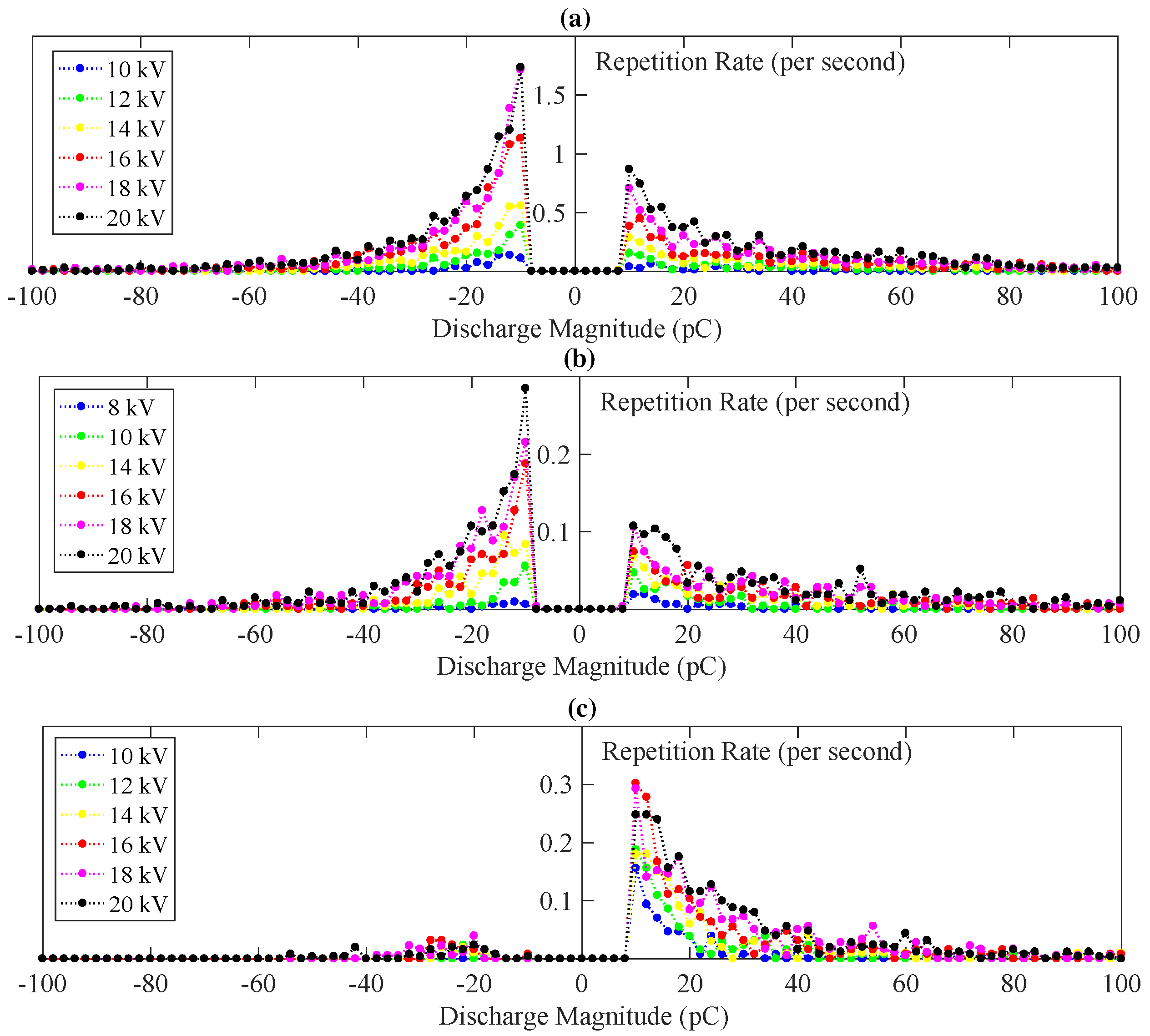
4. Void Discharge Behavior with Applied Voltage and Frequency
Experience with the cable sample from
Section 3 showed that the void quickly deteriorated. It was decided to perform the next experiments at a lower frequency range of 0.01–0.1 Hz, thus minimizing the deterioration while studying the trends. A second 5 kV 133% insulation Cu 2 EPR cable sample was prepared with an artificial void of 6 mm diameter and 1 mm depth. However, this time, the void was located at the interface of outer semicon layer and the insulation as highlighted in
Figure 4.
Figure 8 shows the distribution of the PD
with respect to
for different voltage levels from 10 to 20 kV in steps of 2 kV. The results are shown for DC, as well as 0.01 Hz and 0.1 Hz sine wave. The voltages are stated in terms of their peak for sinusoidal voltages. The experiments are conducted at room temperature (22
C). All measurements, done on the same day with DC tests last, are listed as ‘Test Series 1’ in
Table 2. The duration of test and PDIV are reported.
The following trends can be observed:
Both negative and positive PD
have a specific distribution pattern with respect to the
, with a maximum (
) at 10 pC. The distribution is asymmetrical, with negative
having higher values for lower
as compared to positive
. We know that the electric field across the void is asymmetrical due to the relatively large void size and the cylindrical cable geometry [
23]. However, a more convincing reasoning for the asymmetry in distribution comes from considering the material in the role of cathode in each case [
17,
20]. When the inner conductor is at negative polarity (resulting in measured negative PDs), the EPR insulation wall acts as the cathode, thus exhibiting a higher rate of discharges consistent with observations in [
20]. During positive polarity, however, the semicon layer is the cathode, resulting in higher over-voltages, and, therefore, higher discharge magnitudes [
17,
19].
As the applied voltage is increased, the PD
increases for both positive and negative sides. Its distribution pattern with respect to discharge magnitude and the position, where
, occurs does not vary significantly. The theory presented in [
14,
19] supports these observations. Furthermore, the charge decay rate increases with average field across the void, and, therefore, the recovery time decreases [
23].
The value of
increases with applied voltage, but this trend is not always followed. For instance, as we go higher in voltage from 16 kV DC to 20 kV DC in
Figure 8c,
decreases. This behaviour will be further explored in the subsequent section.
As frequency is increased from 0.01 Hz to 0.1 Hz, the
significantly increases. The relationship between
and repetition rate is explained in [
15]. With higher applied frequency, the lag time
is expected to decrease. The position at which
occurs does not change significantly. With higher frequencies, greater levels of over-voltages (on which the
depends) above the PDIV are achievable more quickly. However, with higher over-voltages, the statistical time lag decreases [
22].
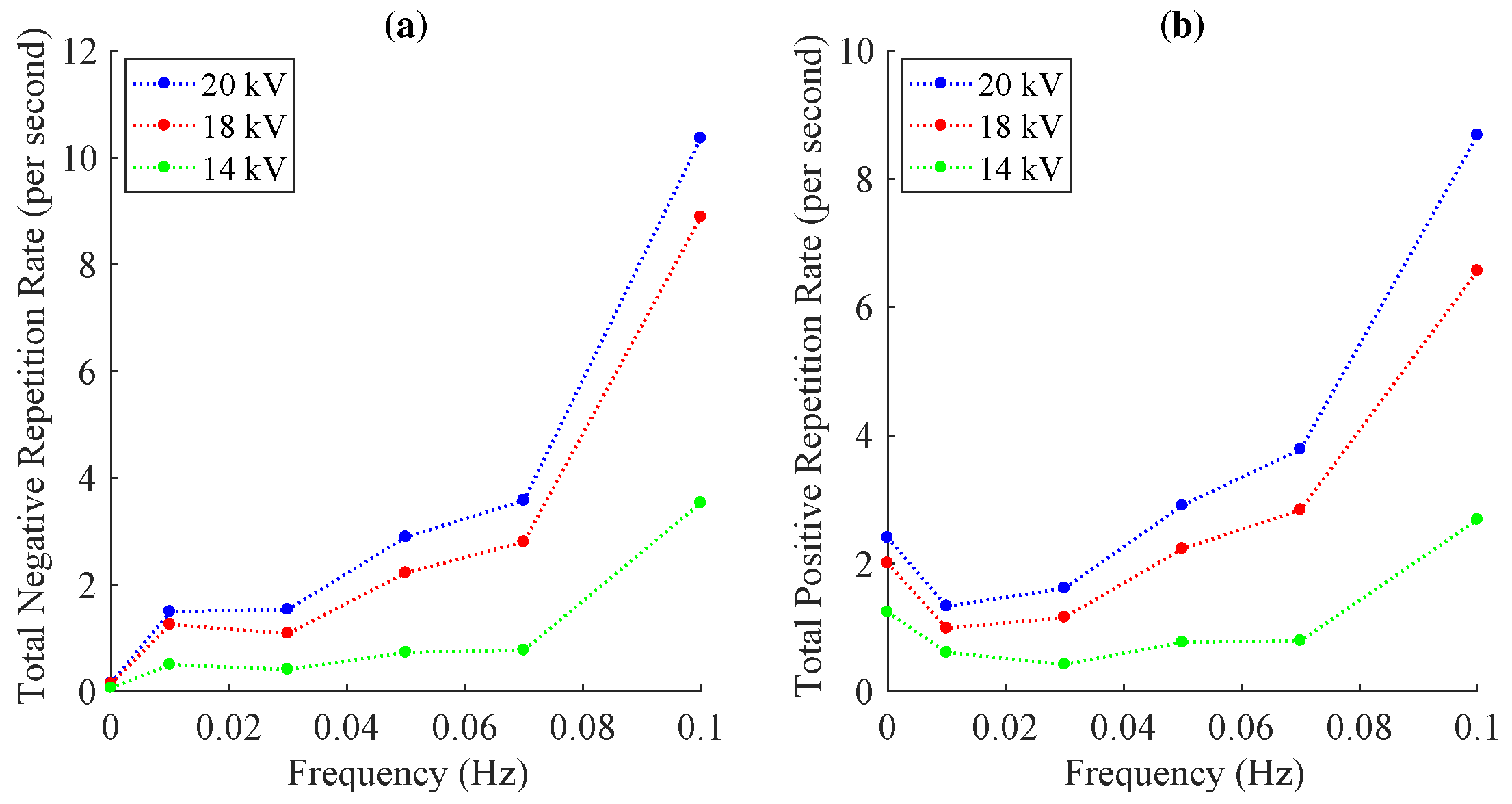
There are only positive PDs under DC conditions, which is expected, as there is no polarity reversal. While negligible PDs can be observed in the negative side, for DC, these signals are considered to be caused by processes outside the cable under test, thus essentially extraneous to our experiment and equivalent to noise. The positive under DC voltages is higher than the positive under 0.1 Hz. However, the sum of positive and negative for 0.01 Hz is greater, indicating that the total PD activity in time is slightly greater than DC.
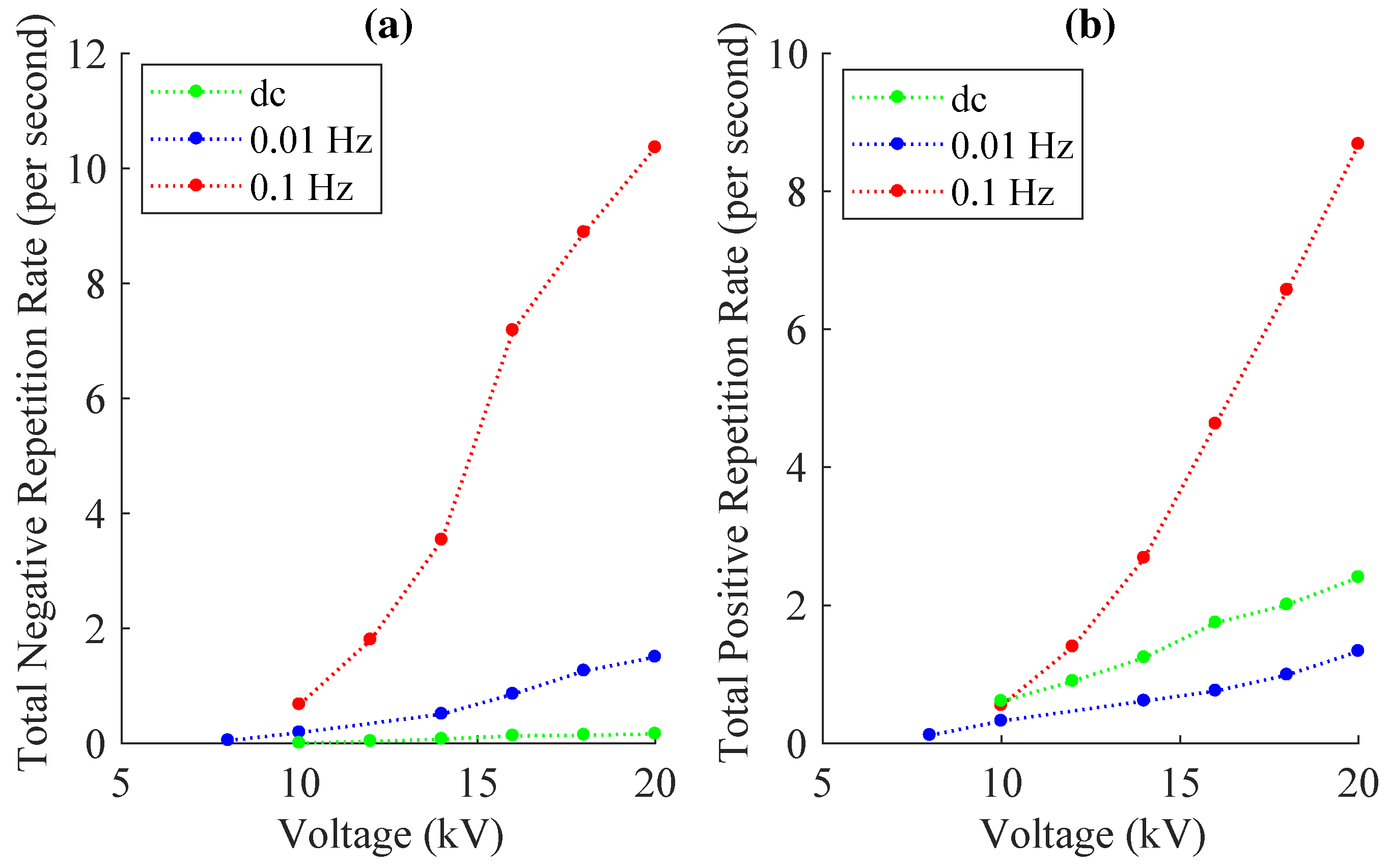
4.1. Voltage Dependence
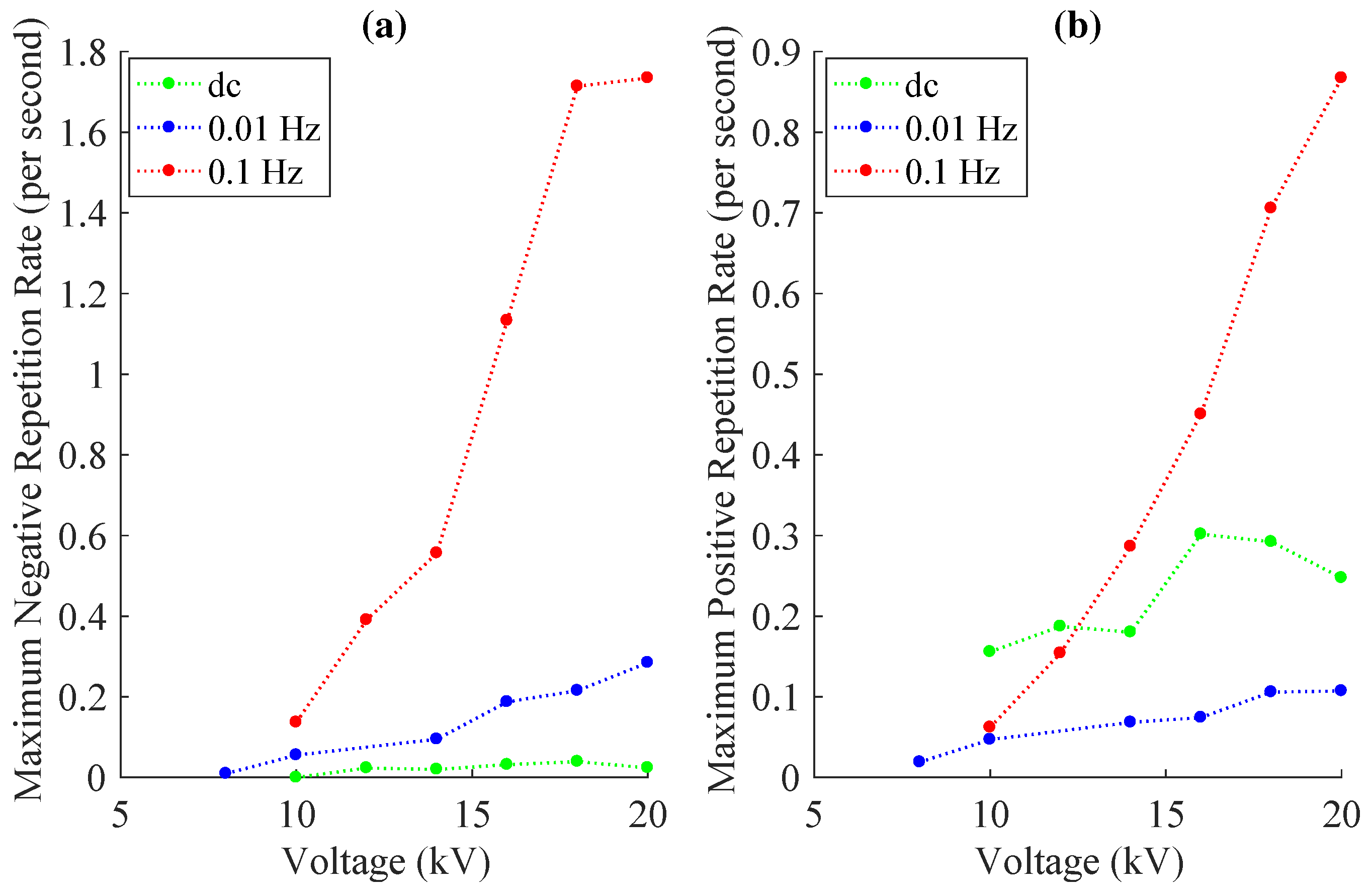
Figure 9a,b describe the trend of negative and positive
with respect to applied voltage.
Results are shown for DC, 0.01 Hz and 0.1 Hz. The sinusoidal voltages are represented by their peak magnitudes. The positive
for DC is higher than that for 0.01 Hz and also for that of 0.1 Hz in the lower voltage range. The negative
is nearly double the positive for both 0.01 Hz and 0.1 Hz. A direct dependence with increasing sinusoidal voltages was observed, but this is not the case with DC, where the trend is less predictable. To derive a deeper understanding,
, the total repetition rate cumulative over all discharge magnitudes, is shown in
Figure 10 with respect to applied voltage.
The following inferences can be drawn:
Under similar applied voltage and frequency conditions, the positive and negative
have comparable values. This observation from
Figure 10, in combination with
Figure 8, possibly implies that the discharges are occurring in the same void with a specific
distribution in
.
The difference in positive and negative
in
Figure 9, in combination with the above inference, indicates that a greater number of higher
positive PDs are present as compared to negative PDs. For negative PDs, a higher number of lower
are observed. This behavior is in agreement with the observations of the role of cathode material described in [
17,
20], leading to asymmetry in the PD activity during positive and negative voltage cycles.
The total PD activity with 0.01 Hz (sum of positive and negative ) is slightly higher than the PD activity under DC conditions.
While the observed trend in under DC conditions was less predictable, consistently increases with voltage.
The frequency dependent increase in
is more significant for voltages higher than the PDIV. While PD repetition rate is an important factor governing the insulation life [
11], inception voltage is also relevant. The inception voltage showed weak dependence on applied frequency in the conditions tested in this study, in agreement with similar observations made in [
18]. It is important to know whether inception voltage of PD activity is above the nominal operating value if the DC voltage enhancement factor, as compared to AC, is to be determined based on the insulation performance over its lifetime.
After the series of tests discussed above (Series 1), two more series of tests were conducted. These test series comprised of experiments conducted on the cable sample to investigate the gradual deterioration due to PD activity. Each series was conducted in one day. The discussion up to this point was based on ‘Test Series 1’. ‘Test Series 2’ was conducted as a verification of the first series and to understand the frequency trend in more detail. Finally, ‘Test Series 3’ was conducted after thermal exposure of the sample to understand the PD behavior after void evolution. Applied voltage was varied from 0–20 kV in steps of 2 kV for each test and the rate distribution over discharge magnitudes was measured for 5 min.
In order to quantify the observed empirical trends numerically, the linear regression tool was used. It should be noted that the parameters presented herein are used solely to study the comparative trends with applied voltages and frequency specific to this study and may change with different operating conditions and void evolution. The theoretical model attempting to derive the underlying physics is discussed in [
32]. To correlate the parameters of the trend-line equation with physical quantities, Equation (
7) was used:
where
is the total PD repetition rate (either positive or negative) in s
dependent on the applied voltage and frequency and
is the peak of the applied voltage in kV. The slope m is the variation of
with respect to the applied voltage with units
. The constant term
is the estimated PDIV in kV. The slope m and constant term
are the parameters estimated using regression analysis to fit the linear equation defined in Equation (
7) onto the measured variation in total PD repetition rate with peak applied voltage at different frequencies. The results of the regression analysis are presented in
Table 2. The parameters were obtained from the curve fitting tool of MATLAB (R2016b, The Mathworks, inc., Natick, MA, USA), including the coefficient of determination (
) indicating the goodness of fit. Time for which the experiment was conducted and the observed PDIV
are also tabulated.
The high value, greater than 0.95 and sometimes as high as 0.99, indicates acceptable confidence on the goodness of fit of the proposed linear relationship between total PD repetition rate with applied peak voltage. The slope m for DC is double that for positive in case of 0.01 Hz, mathematically supporting the empirical inference that the time for which HV is imposed governs the PD behavior. At this extremely low frequency, the influence of on PDs is not observable. Furthermore, sinusoidal polarity reversal every 50 s does not significantly affect the discharge behavior in terms of and its variation with peak applied voltage as compared to DC. The PDIV is also similar.
In order to gain statistical significance of the linearity of
with applied voltages that curve fitting indicates, further experiments were conducted for PD activity at 0.03 Hz, 0.05 Hz and 0.07 Hz and different voltage levels. These are listed under ’Test Series 2’ in
Table 2. The experiments suggest a strong linear relationship between
-
at all measured frequencies, within the voltage range studied. These results also offered insight on the frequency dependence of PD activity, which is discussed in the subsequent section.
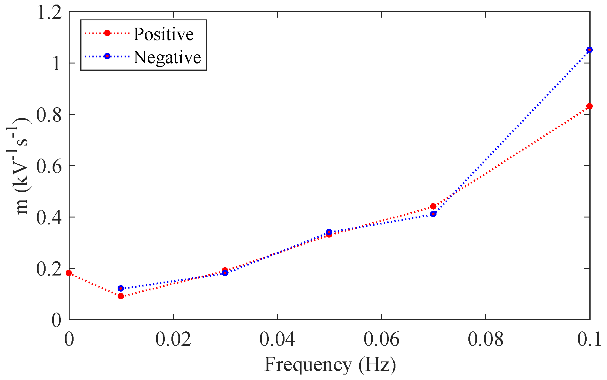
4.2. Frequency Dependence
Figure 11 shows that the slope of the voltage variation in both positive and negative
nonlinearly increases as the applied frequency is increased.
This increase showcases the greater influence of than the PDIV on the PD activity. The nonlinearity is understandable, considering that the time for which the voltage is higher than inception, as well as the imposed during such voltages, are nonlinear functions of frequency. It cannot be inferred from these results, however, whether the effect of itself on the PD activity is nonlinear. Addressing this question is relevant from a transient behavior standpoint but is beyond the scope of this research.
Furthermore, evidence suggests that the void gradually evolves, leading to higher PDIV and lower PD repetition rates with higher discharge magnitudes. Such observations and their possible reasons were also reported in [
24]. Since tests for 0.03 Hz, 0.05 Hz and 0.07 Hz were conducted later, the artificial void had already been subjected to considerable aging under HV. The evidence of void evolution is revisited in the subsequent section. In
Figure 12, the results for frequency variation in
for select applied voltages are shown.
The nonlinear dependency of PD activity on frequency is visible in this figure. The slope is similar for positive and negative PD activity. From the results, there is no clear trend indicating that one is discernibly higher than another at this voltage and frequency range.
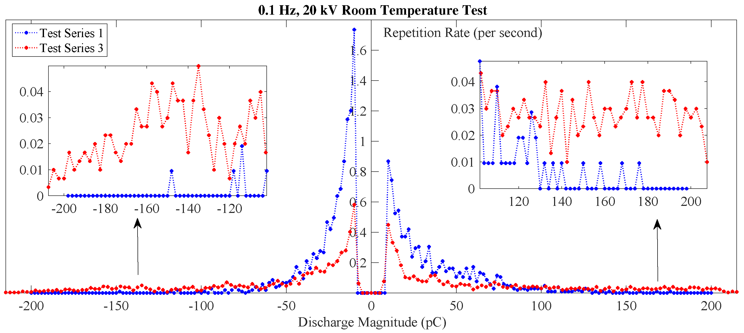
4.3. Void Evolution
Low frequency was used to study the trends in PD activity while minimizing their deleterious effect on AC voltages. It is, however, also interesting to see how the void evolves in time. After imposing high temperature (HT) (measured 60
C at the sheath), post-thermal, room temperature tests were conducted. These are presented as ‘Test Series 3’ in
Table 2. The repetition rate distribution with discharge magnitude for different voltages in ‘Test Series 3’ is shown for 0.1 Hz, 0.01 Hz and DC in
Figure 13.
It can be observed that the repetition rate is significantly lower as compared to those presented in
Figure 8. It was observed that the PDIV had significantly increased as compared to ‘Test Series 1’. For 0.1 Hz and 0.05 Hz, the inception was observed at 12 kV, while, for 0.01 Hz, it was at 18 kV. For DC, no positive PD was observed even at the maximum imposed voltage of 20 kV. It is possible that the space charges and conductivity change are playing a role as predicted in [
24,
25]. Observations suggest that ageing resulted in EPR conductivity larger than the unaged case in the vicinity of the void since it is much easier to induce space charge at the same voltage level. Since 20 kV is applied on a 5 kV cable (2.9 mm insulation thickness), considerable space charges can develop [
33]. Specific to the voids at the semicon-dielectric interface of the cable, evolution of voids are accompanied by metal migration towards the dielectric material. This erosion changes the conductivity of the void walls, leading to change in PD behavior. For example, the copper content at the EPR surface was 0.2% [
24]. The similar phenomenon could be expected with the semicon-interface.
Figure 14 shows the distribution of PD
with respect to
for 0.1 Hz sinusoidal AC from Test Series 1 and 3 measurements.
It can be observed that the total PD rate is significantly lower with ageing. There is, however, an increase in the PDs at higher discharge magnitudes. This is consistent with the observations in [
24].
5. Conclusions
The PD activity in the artificial void at the semicon-dielectric interface has been observed to linearly increase with applied voltage in the range 10–20 kV for 0.01–0.1 Hz frequencies as well as DC. The maximum of repetition rate distribution over the discharge magnitude occurred at 10 pC and did not shift position with varying applied voltage and frequency. The increase in repetition rate with frequency appeared nonlinear, but this could be due to the void evolution.
The density distribution of PD repetition rate was asymmetrical, with negative PDs having a higher maximum of repetition rate distribution over the discharge magnitude, but positive PDs having higher repetition rate at higher discharge magnitudes as compared to the negative PDs. Similar evidence was reported in [
17,
20]. The total repetition rates, however, were found to be comparable.
In the initial tests, the total PD repetition rate at DC voltage was lower as compared to AC sinusoidal voltage. However, it was observed to be comparable to 0.01 Hz AC voltage results. The PDIV did not exhibit observable frequency dependence. Therefore, it is important to know whether the PDIV is above the nominal operating value if the DC voltage enhancement factor as compared to AC is to be determined based on the insulation performance over its lifetime.
In agreement with the preliminary tests using 60 Hz AC sinusoidal wave on the 5 kV Cu 2/0 EPR cable, the second sample (5 kV Cu 2/0 EPR cable) showed signs of gradual deterioration over time even when subject to low frequencies. The PD activity had lower repetition rate and higher PDIV after a high temperature exposure at 60
C, while, at the same time, higher discharge magnitudes were observed. No PD activity was seen until 20 kV with DC voltage at room temperature after the void had evolved. This could possibly indicate the change in void surface conductivity and effect of space charges predicted in [
25] due to the phenomenon of semiconductor layer material migration consistent with the observations of [
24].
The main observation is that the PD rate under DC voltage is significantly lower than that under 0.1 Hz and 60 Hz AC sinusoidal voltages with the same peak value. The intentional void did evolve over time, especially under the thermal exposure. The preliminary observation and test experience on medium voltage cables with intentional defects made us gain more confidence on our hypothesis that DC voltage helps to reduce cable weight/volume as compared with 50/60 Hz voltages. Obviously, more extensive experimental tests and theoretical investigations are still required to support this hypothesis.

 ,
, 


