Article

A Novel WPT System Based on Dual Transmitters and Dual Receivers for High Power Applications: Analysis, Design and Implementation

1
School of Electrical Engineering, Southwest Jiaotong University, Chengdu 610031, China
2
School of Engineering and Computing Sciences, Durham University, Stockton Road, Durham DH1 3LE, UK
*
Author to whom correspondence should be addressed.
Energies 2017, 10(2), 174; https://doi.org/10.3390/en10020174
Submission received: 14 October 2016 / Revised: 30 December 2016 / Accepted: 19 January 2017 / Published: 4 February 2017
(This article belongs to the Special Issue Wireless Power Transfer 2016)

Abstract

:
Traditional Wireless Power Transfer (WPT) systems only have one energy transmission path, which can hardly meet the power demand for high power applications, e.g., railway applications (electric trains and trams, etc.) due to the capacity constraints of power electronic devices. A novel WPT system based on dual transmitters and dual receivers is proposed in this paper to upgrade the power capacity of the WPT system. The reliability and availability of the proposed WPT system can be dramatically improved due to the four energy transmission paths. A three-dimensional finite element analysis (FEA) tool ANSYS MAXWELL (ANSYS, Canonsburg, PA, USA) is adopted to investigate the proposed magnetic coupling structure. Besides, the effects of the crossing coupling mutual inductances among the transmitters and receivers are analyzed. It shows that the same-side cross couplings will decrease the efficiency and transmitted power. Decoupling transformers are employed to mitigate the effects of the same-side cross couplings. Meanwhile, the output voltage in the secondary side can be regulated at its designed value with a fast response performance, and the system can continue work even with a faulty inverter. Finally, a scale-down experimental setup is provided to verify the proposed approach. The experimental results indicate that the proposed method could improve the transmitted power capacity, overall efficiency and reliability, simultaneously. The proposed WPT structure is a potential alternative for high power applications.

1. Introduction

Wireless power transfer technology is a promising approach to deliver power from power source to loads without physical contact [1,2,3,4]. It has been employed for various applications including biomedical implants [5,6], mining applications [7], under-water power supply [8] and electric vehicles [9,10,11,12,13,14] with the advantages of being unaffected by ice, water or other chemicals.
Nowadays, the demand for high power application is on the rise. The converters on both primary and secondary sides must essentially be capable of handling the required power level. However, the power capacity of a traditional WPT system is limited by the constraints of semiconductor devices. Besides, the single transmitter and single receiver based magnetic coupling structure results in a low reliability of the WPT system due to the only one energy transmission path, and it unlikely meets the requirement of high power applications since public transport systems need to be rated at hundreds of kVA or more (up to MW scale) [14]. Therefore, it is significant to investigate approaches which can enhance the transmitted power of WPT systems by using low-power and low-cost semiconductor devices for high power application e.g., railway transport (electric trains and trams, etc.) [14].
The operating frequency of the inverter can be increased to enhance the power transmitted to the load. However, it is limited by both switching losses and switching speed limitations of power semiconductors adopted in the inverter. Alternatively, increasing of the mutual inductance between the transmitter and receiver might be one of the possible solutions to upgrade the maximum transmitted power. However, the way to increase mutual inductance is to narrow the air gap between the transmitter and the receiver, to add more ferrites, to adopt more turns, and/or to change the structure of the receiver. In some applications, it is not feasible to adopt the aforementioned methods due to the cost and the installation space limitations. Moreover, a large size coil with large inductance will result in a high voltage across the coil due to the resonance. Similarly, a high transmitter current is preferable for high-power WPT systems. However, it is a big challenge to generate such a high current in the transmitter because of the limitation of the power rating and cost of the semiconductor devices.
Therefore, some approaches have been proposed to address the aforementioned issues. The multilevel converter topology would be an alternative solution due to its advantages in terms of reducing the voltage stress of semiconductor devices and increasing the output power capacity. Phase shift pulse width modulation method has been employed in cascaded multi-level inverter supplying WPT systems to realize power regulation and selective harmonic elimination, simultaneously [15]. However, the cascaded structure of multi-level inverter dramatically decreases the reliability of WPT systems. Another approach is to use multi-inverter connected in parallel to provide an amount of high frequency current to supply the transmitter of WPT systems. A parallel topology is proposed for WPT systems [16], which can achieve high output power levels in a cost effective manner. Moreover, it has a high reliability of functioning, even that a faulty parallel unit is electronically shut down. An active and reactive currents decomposition based control method is proposed to suppress the circulating currents among the parallel inverters [17], and the WPT system can continuously work with faulty inverter units.
Some approaches using multiple transmitters to power a single receiver have been investigated in [18,19,20,21]. There is an increase in gain of the transmitted power due to the increase number of transmitters. In order to improve the induced voltage, a practical power line synchronization technique is proposed to synchronize all transmitters [18]. Magnetic couplings among the transmitters is non-negligible when the transmitters located close to each other. The effect of couplings among the multiple transmitters is discussed in [19]. The resonant frequencies are changed due to the magnetic coupling among the transmitters, which dramatically decrease the transfer efficiency. A novel WPT topology based on dual coupled transmitters is proposed in [20]. By configuring the additional compensation capacitors, resonant inverters with different power ratings can be connected in parallel to achieve a high power transfer. A stable power transfer efficiency region under two transmitters scenario by using efficient, electrically small, folded cylindrical helix dipoles is created [21]. Moreover, the stable power transfer efficiency region can be extended to two-dimensional space by using four transmitters. However, previous researches only adopted one receiver in the secondary side to pick up the power, which hardly meet the power demand due to capacity constraints of secondary side power electronic devices. Besides, it suffers a low reliability, which is not a good choose for railway application. A multi-antenna system acted as a power transmitter to provide a better effective coverage for a wearable and wireless neurotransmitter sensor recording system is designed and demonstrated [22], but the module is only operated in low-power implantable devices.
Some approaches using a single transmitter to power multiple receivers have been investigated in [23,24,25]. A single transmitter charging multiple receivers based WPT systems are provided [23], which are suitable for devices such as mobile phones that do not need highly accurate tuning. A relatively simple circuit description is used in [24] to model resonant coupling systems with multiple receivers. In addition, a power transfer system focusing upon the resonant frequency splitting issues that arise in multi-receiver applications is demonstrated. To design a high efficiency Single Input Multiple Outputs (SIMO) system, a method which is optimization by impedance matching at transmitting circuit is propose [25]. However, previous researches only adopted one transmitter in the primary side to transfer the power, which hardly meet the power demand due to capacity constraints of primary side power electronic devices and lack of reliability. Besides, in previous researches, each receivers connects to one independent load, which do not gather received power together to power one load for high power applications.
Some approaches using multiple transmitters to power multiple receivers have been investigated in [26,27,28]. The splitting frequency analysis and the use of chirp signals to spread data and excited inductive Multiple Inputs Multiple Outputs (MIMO) WPT systems are presented in [26]. Modular-based WPT systems are proposed to cater for high power applications by integrating multiple WPT systems [27]. Inductive power transfer between M primary coils coupled to N secondary coils is derived analytically and demonstrated experimentally for M = 1, 2 and N = 1, 2, 3 in [28]. Unfortunately, all the researches mentioned above, the crossing couplings among transmitters and receivers are neglected and the coupling structure is not suitable for railway applications.
WPT Systems proposed in [29,30,31] consist of one source coil, multiple self-resonators and one load coil. A WPT system with four resonant coils is presented in [29], which is designed and implemented for the power supply of micro-implantable medical sensors. The system proposed in [30] consists of a transmitter with five self-resonators and a receiver with a self-resonator which supports free positioning in a large area. An optimal design method in an asymmetric wireless power transfer system for a 150 watt LED TV is discussed in [31] where the system consists of three self-resonators: a Tx resonator, an Rx resonator, and an intermediate resonator. However, in those researches, there is only one power transmitting path to power the load which is lack of reliability and not enable to power high power applications.
A poly-phase bidirectional inductive power transfer system used for EV charging is proposed by [32] to enhance the misalignment ability and power level. However, the output voltage control and redundancy analysis are missed and the method to mitigate the effects of cross coupling is ignored. The effects of crossing couplings among transmitters of polyphase WPT systems are analyzed, and three methods are presented to eliminate the effects of the crossing couplings [33]. However, the control and redundancy design of the poly-phase WPT system are ignored.
This paper attempts to enhance the power capacity of the WPT system and improve the system’s reliability, and a novel WPT topology which consists of dual overlapped transmitters connected with two isolating inverters and dual receivers of which outputs are connected in parallel to power the load is proposed. The inverters that feed the corresponding transmitter can be designed and manufactured in large quantities to reduce the manufacturing cost, because redesigning and manufacturing an inverter is usually a time-consuming and expensive process [17]. Besides, the limitation of single resonant inverter unit can be alleviated in terms of cost, heating dissipation, component limitation, and short time overload. The work presented in this paper lays claim to the contributions as follows:
(1)
A novel WPT system with high reliability based on dual overlapped transmitters and dual receivers are proposed to enhance the transmitted power, which is a potential method for high power applications.
(2)
The effects of same-side couplings are analyzed by the equivalent circuit, and decoupling transformers are adopted to eliminate the effects of same-side couplings. As a result, the WPT system can maintain a constant resonant frequency.
(3)
The output voltage in the secondary side can be regulated at its designed value with a fast response performance by the designed controller.

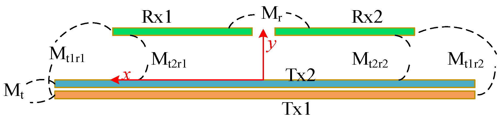
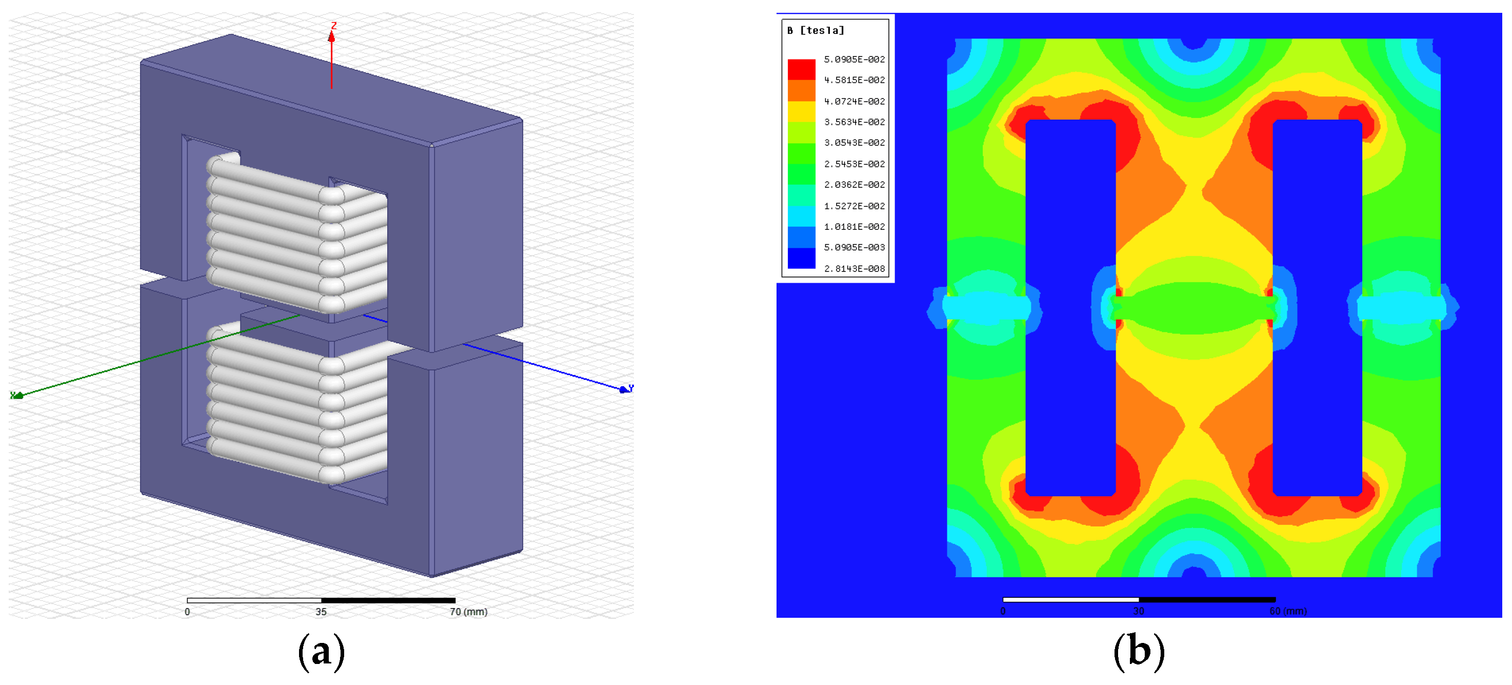
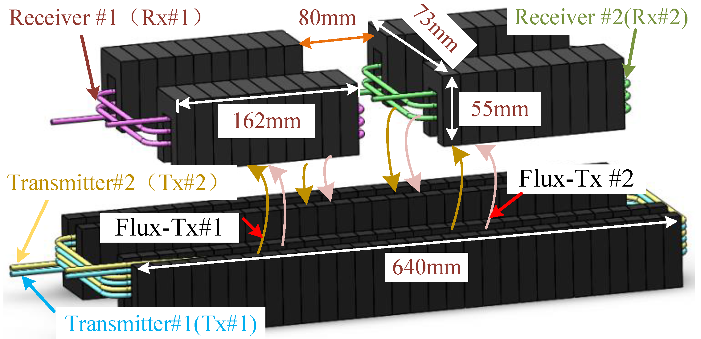
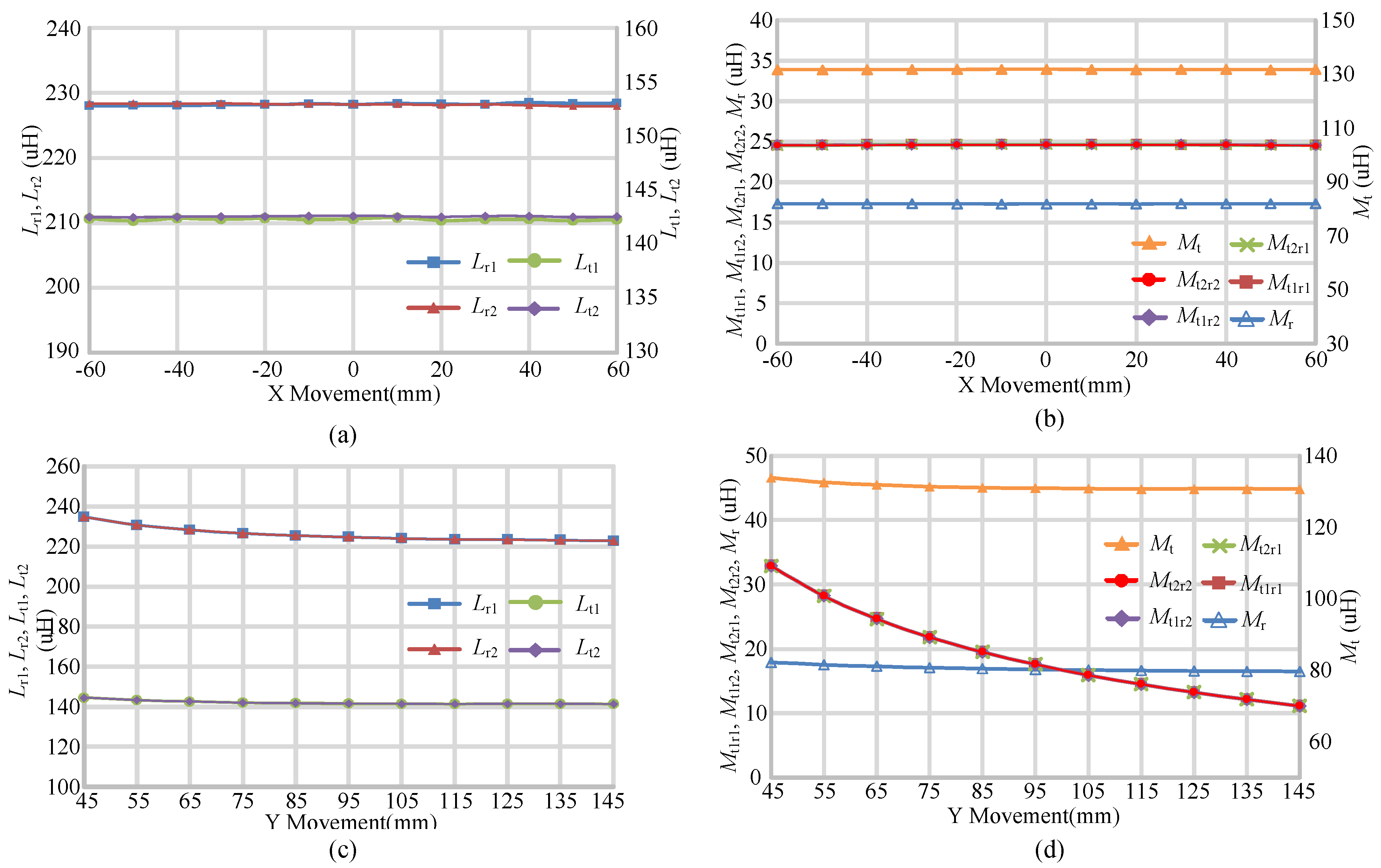
2. Proposed Magnetic Coupling Structure

In the some practical applications, the receiver coil’s size is limited by the installation space of the bottom of the vehicle. Therefore, there may not be sufficient space to install a big size receive coil. Moreover, large size coil with large self-inductance will result in a high voltage due to the resonance. However, a small size receiver coil will result in a low coupling coefficient and a limitation for the output power of the WPT system. So dual small size receivers with low self-inductance can be employed to capture the magnetic field. The basic motivation of the proposed structure was to gather the transmitters together to share the ferrite cores to generate an enhanced magnetic field, and dual small size receivers placed on the top of the transmitters to capture the magnetic flux.
Figure 1 shows the structure and dimensions of the WPT system based on two transmitters and two receivers, where the transmitters are totally overlapped and located close to each other and the receivers are placed on the top of the transmitters to capture the magnetic field around the transmitters. The transmitters are embedded on the ground and the receivers are installed on the bottom of vehicle.
As can be seen from Figure 1, the total magnetic field intensity around the transmitters is synthetized by the magnetic field intensity generated by the transmitter #1 and the transmitter #2. Therefore, the total magnetic field intensity can be enhanced by using dual transmitters due to the overlapped magnetic coupling structure. Furthermore, in order to enhance the coupling mutual inductances between the transmitters and the receivers, all the transmitters and receivers are wound around U-type ferrite cores as [14] did. It is worth noticing that the ferrite cores can be any other types e.g., E-type, and/or I-type for various applications.
In this case, all the transmitters and receivers are inevitably coupled with each other due to the coils’ loosely coupled nature. Therefore, transmitter #1 can transfer energy to receiver #1 and receiver #2, simultaneously. Accordingly, Transmitter #2 can transfer energy to receiver #1 and receiver #2. As a result, there are basic four energy transmission paths.
Some basic design considerations of the coils should be explored. First of all, the same shape and turns are chosen intuitively for the dual transmitters. Second, the dual receivers are identical and they are deliberately designed shorter than the transmitters, so that it can dynamically move over the transmitters freely. Third, a 3-D FEA tool ANSYS MAXWELL is utilized to model the proposed magnetic coupling structure. The magnetic coupling structure with the transmitter coil sized at 640 mm × 73 mm with seven turns, the receiver coil sized at 162 mm × 73 mm with sixteen turns and vertical air gap of 70 mm is modelled. The separation distance between the dual receivers is chosen to be 80 mm accordingly.
This study is focused on the coil inductances, the cross-side coupling mutual inductances, and the same-side coupling mutual inductances. The cross-side coupling mutual inductances Mtirj are defined as the coupling mutual inductances between the transmitter #i (i = 1, 2) and the receiver #j (j = 1, 2) distributed on different sides, while the same-side coupling mutual inductances indicate the coupled coils are coming from the same side. Mt, Mr are same-side coupling mutual inductances of transmitters and receivers. Lt1, Lt2, Lr1 and Lr2 are the self-inductances of the transmitters and receivers. The schematic diagram of cross couplings among the coils is shown in Figure 2. It should be noted that the dual transmitters are completely overlapped with no air gap in the practical system. However, the air gap between the transmitters shown in Figure 2 is used to illustrate the couplings.
The variations of the mutual inductances and self-inductances are very important to the circuit modeling. The proposed WPT system can be used for railway application, which only have two direction misaligned situations due to the railway track. The misaligned situations along the x-axis and y-axis are illustrated, respectively, in the FEA tool. The FEA simulation results are shown in Figure 3, and it should be noted that the coordinates in Figure 3 are defined as indicated in Figure 2. The cross-side coupling mutual inductances, same-side coupling mutual inductances and self-inductances are stable along x-axis misalignment. The cross-side coupling mutual inductances are approximately identical. It can be observed that the self-inductances are slightly affected by the y-axis misalignments. The cross-side coupling mutual inductances drop with the increase of vertical air gap. However, the cross-side coupling mutual inductances are identical to each other with various vertical air gap.

3. Analysis of the Proposed WPT System

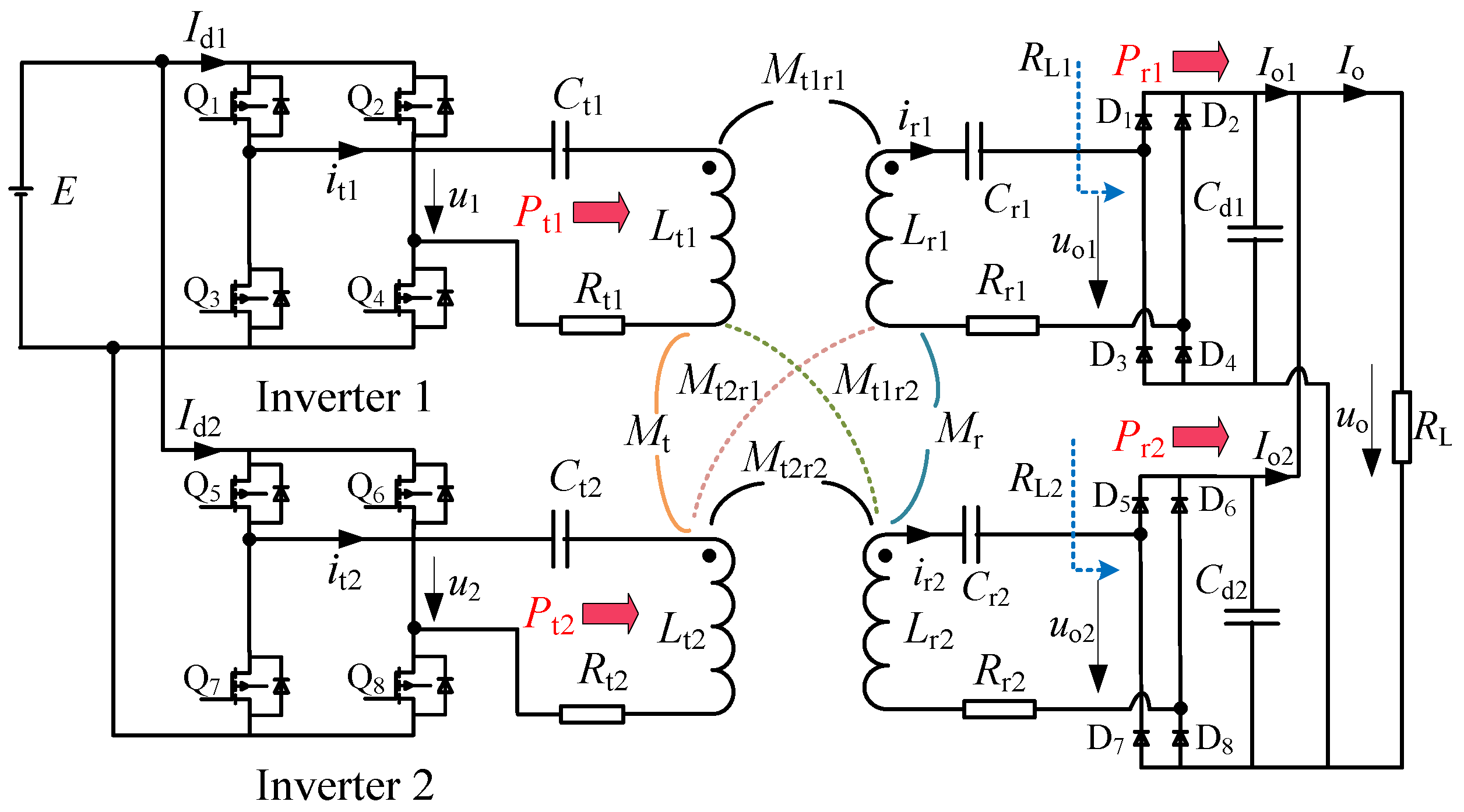
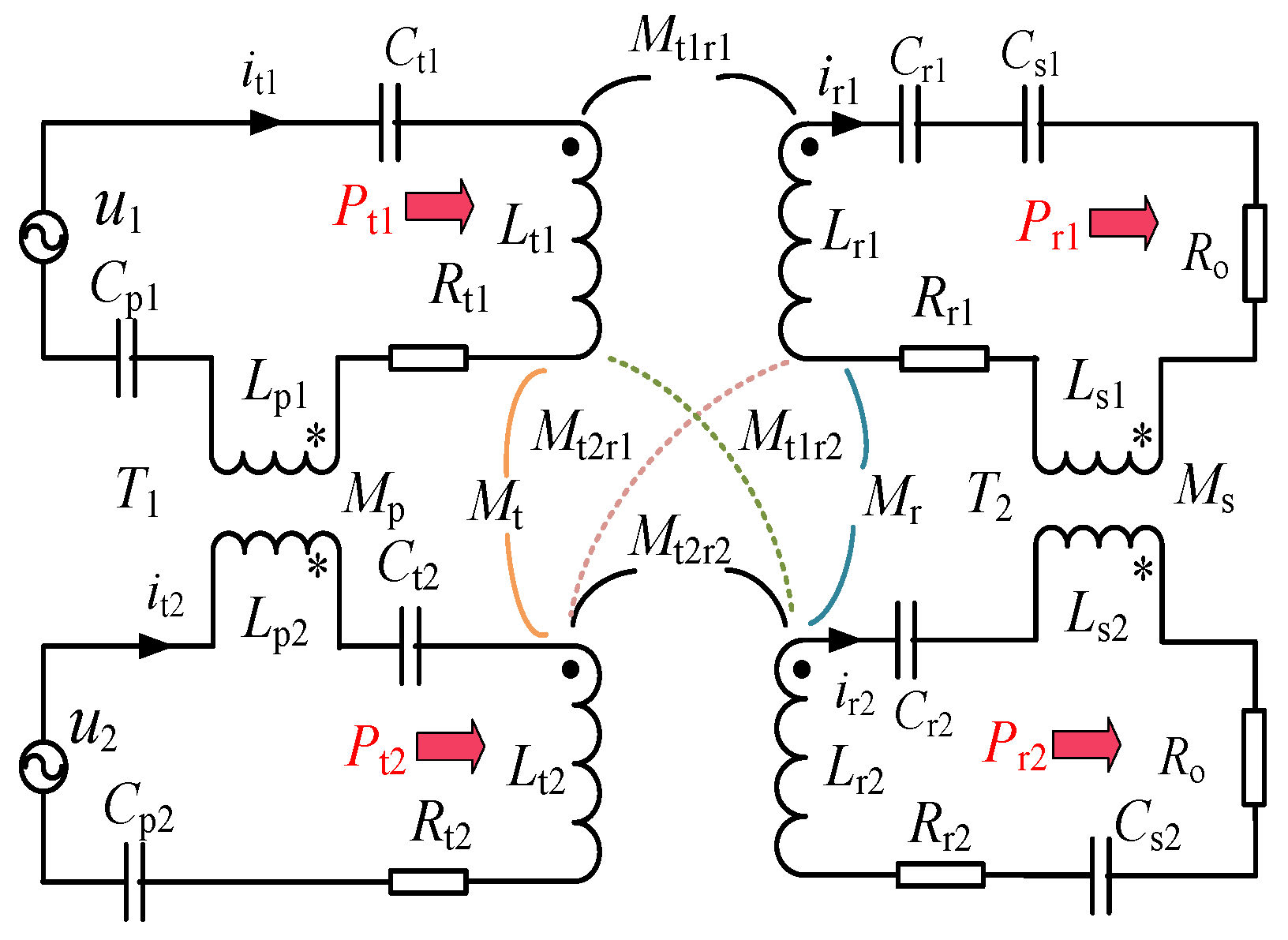
3.1. Circuit Modeling

Based on the FEA results presented in Section 2, the circuit topology of the proposed WPT system can be shown in Figure 4. Each transmitter is connected with a resonant inverter, and the inverters share a common DC source. In accordance with the transmitters, each receiver is connected with a rectifier which converts the high frequency voltage induced within the receiver into DC voltage. The outputs of the rectifiers are connected in parallel to power the load RL.
Series compensations are employed for both primary and secondary sides to compensate the reactive power caused by the leakage inductance. Ct1, Ct2, Cr1 and Cr2 are the compensation capacitors of the transmitters and receivers respectively. Rt1, Rt2, Rr1 and Rr2 are the parasitic resistances of the transmitters and receivers. Defining RL1, RL2 as the equivalent resistance of two rectifiers respectively. To focus on the feasibility analysis, the fundamental harmonic approximation will be applied under static-state conditions.
The inverters generate a fixed-frequency ac output voltage u1 and u2 to power the corresponding transmitter, and the inverters are controlled by the phase-shift technique. Moreover, the voltages are identical with each other by employing Synchronous control technology [16,20], as shown in Figure 5. The fundamental voltage phasor of inverters can be derived as:
U ˙ = U ˙ 1 = U ˙ 2 = 2 2 E sin ( θ L ) π
According to mutual coupling theories, the relationships between the currents and the voltages can be described following the Kirchhoff’s voltage law (KVL):
[ U ˙ 1 U ˙ 2 0 0 ] = [ Z t 1 j ω M t j ω M t 1 r 1 j ω M t 1 r 2 j ω M t Z t 2 j ω M t 1 r 1 j ω M t 1 r 2 j ω M t 1 r 1 j ω M t 1 r 2 Z r 1 j ω M r j ω M t 1 r 1 j ω M t 2 r 2 j ω M r Z r 2 ] [ I ˙ t 1 I ˙ t 2 I ˙ r 1 I ˙ r 2 ]
where:
{ Z t 1 = j ω L t 1 + 1 j ω C t 1 + R t 1 Z t 2 = j ω L t 2 + 1 j ω C t 2 + R t 2 Z r 1 = j ω L r 1 + 1 j ω C r 1 + R r 1 + R L 1 Z r 2 = j ω L r 2 + 1 j ω C r 2 + R r 2 + R L 2
The self-inductances of the transmitters and receivers are completely tuned by the series compensation capacitors, i.e.,:
{ j ω L r i + 1 j ω C r i = 0 j ω L t i + 1 j ω C t i = 0   ( i = 1 , 2 )
As mentioned previously, the structures of the transmitters are designed identically and the self-inductances are constants as simulated. In addition, the cross-side coupling mutual inductances are approximately identical, i.e., Mt1r1 = Mt1r2 = Mt2r1 = Mt2r2 = M. The parasitic resistances of the transmitters are identical to Rt and the parasitic resistances of the receivers are identical to Rr.
According to [34], the equivalent resistances of two rectifiers connected in parallel are identical:
R L 1 = R L 1 = 16 π 2 R L = R o
Substituting Equations (3), (4) and (5) into Equation (2), the relationships of currents and voltages can be derived as:
{ I ˙ t 1 = I ˙ t 2 = ( M r 2 M j R o + R r 2 ω M ) I ˙ r 1 = ( M r 2 M j R o + R r 2 ω M ) I ˙ r 2 U ˙ 1 = [ R t + 4 ω 2 M 2 ( R o + R r ) ω 2 M 2 + ( R o + R r ) 2 + j ω 3 M 2 ( M t M r ) + ω M t ( R o + R r ) 2 ω 2 M 2 + ( R o + R r ) 2 ] I ˙ t 1
With these relationships, the input impedances of the system can be derived as:
Z IN 1 = Z IN 2 = U ˙ 1 I ˙ t 1 = U ˙ 2 I ˙ t 2 = R t + 4 ω 2 M 2 ( R o + R r ) ω 2 M 2 + ( R o + R r ) 2 + j ω 3 M 2 ( M t M r ) + ω M t ( R o + R r ) 2 ω 2 M 2 + ( R o + R r ) 2
It can be seen that the same-side coupling mutual inductances can make input impedances be either capacitive or inductive instead of resistive, which indicates that the inverters do not work under resonant condition. Consequently, capacitors used to compensate the transmitter and receiver as traditional method do cannot meet the requirement of resonance in the proposed WPT system due to the same-side couplings.
The received power by the receivers and output active power provided by the inverters can be expressed as:
{ P r 1 = P r 2 = | I ˙ r 1 | 2 R o = | I ˙ r 2 | 2 R o P t 1 = P t 2 = Re ( U ˙ 1 I ˙ t 1 * ) = Re ( U ˙ 2 I ˙ t 2 * )
where Re (*) represents the real part of a complex number.
The efficiency of the system can be derived as:
η = P r 1 + P r 2 P t 1 + P t 2 = 4 ω 2 M 2 R o ( R o + R r ) ( 4 ω 2 M 2 + R o R t + R t R r ) + R t ω 2 M r 2
As can be seen from Equation (9), the system efficiency has no relation to Mt, but it is a function against Mr as it is a part of the denominator of Equation (9). It means that the larger the coupling mutual inductance in the receiver sides is, the lower the system’s efficiency will be. Therefore, Mr is needed to be suppressed as much as possible in order to improve the system efficiency. It should be noted that the total power losses consist of the losses of inverter units and the rectifiers, so the measured efficiency is lower than that of the theoretical analysis shown in Equation (9). The measured power losses distribution will be depicted in the Section 4.

3.2. Characteristic Analysis with Decoupling Transformers

As mentioned above, the same-side coupling mutual inductances not only brings extra reactive power, but also lowers power efficiency. These same-side coupling mutual inductances induce voltages within each transmitter and receiver. In order to eliminate the effects of the same-side coupling mutual inductances, decoupling transformers are utilized to induce opposite voltages to cancel out the induced voltages caused by the same-side coupling mutual inductances. A decoupling transformer T1 (the self-inductances are Lp1 and Lp2) is connected in series with the transmitter #1 and transmitter #2 shown in Figure 6. Mp is the mutual inductance of T1 which is designed to be identical to Mt. Similarly, a decoupling transformer T2 is adopted in the secondary side and Ms is designed to be equal to Mr. The parasitic resistances of T1 and T2 can be neglected compared to the load. The decoupling transformers can be realized with the help of ferromagnetic cores, which can achieve the required mutual inductance with less litz wires. Besides, the FEA tool by Maxwell can be employed to accurately determine the final turns of the decoupling transformers. The model established in MAXWELL is shown in Figure 7. By varying the turns of the decoupling transformers T1 and T2, the identical or approximately identical mutual inductances (Mp = Mt and Ms = Mr) can be achieved. The magnetic field distribution of the designed transformer is shown in Figure 7.
It should be noted that the measurement results may be slight different with the simulation results due to the fabrication imperfection. Therefore, it is highly recommended to build and measure the mutual inductance after simulation and slightly change the turns. Additional capacitors are employed to compensate the self-inductances of T1 and T2:
ω = 1 L p 1 C p 1 = 1 L p 2 C p 2 = 1 L s 1 C s 1 = 1 L s 2 C s 2
The relationships between the currents and voltages can be rewritten as:
[ U ˙ 1 U ˙ 2 0 0 ] = [ Z t 1 j ω ( M t 1 t 2 M p ) j ω M t 1 r 1 j ω M t 1 r 2 j ω ( M t 1 t 2 M p ) Z t 2 j ω M t 2 r 1 j ω M t 2 r 2 j ω M t 1 r 1 j ω M t 2 r 1 Z r 1 j ω ( M r 1 r 2 M s ) j ω M t 1 r 2 j ω M t 2 r 2 j ω ( M r 1 r 2 M p ) Z r 2 ] [ I ˙ t 1 I ˙ t 2 I ˙ r 1 I ˙ r 2 ]
Solving Equation (11) gives:
{ I ˙ t 1 = I ˙ t 2 = j R o + R r 2 ω M I ˙ r 1 = j R o + R r 2 ω M I ˙ r 2 U ˙ 1 = U ˙ 2 = [ R t + 4 ω 2 M 2 ( R o + R r ) ω 2 M 2 + ( R o + R r ) 2 ] I ˙ r 1
With these relationships, the input impedances of the system can be rewritten as:
Z IN 1 = Z IN 2 = U ˙ 1 I ˙ t 1 = U ˙ 2 I ˙ t 2 = R t + 4 ω 2 M 2 R o + R r
It is evident that the inverters work under resonant condition and the inverters only provide active power to the load.
The efficiency of the system with the decoupling transformers can be derived as:
η = P r 1 + P r 2 P t 1 + P t 2 = 4 ω 2 M 2 R o ( R o + R r ) ( 4 ω 2 M 2 + R o R t + R t R r )
The efficiency can be improved by using the decoupling transformer in the receiver side, and using decoupling transformers simplifies the analysis of the power transfer characteristics which makes it straightforward to design and control the system.

3.3. Conduction Losses Estimation

The system efficiency can be improved by decoupling transformers. However, the parasitic resistances of the transmitters and receivers will decrease the efficiency according to Equation (14). Therefore, parasitic resistances of the transmitters and receivers should be designed as small as possible. Litz wire with low parasitic resistance is usually used to construct the coils to achieve low power loss and low temperature rise in the transmitters and receivers. Besides, the decoupling transformers should be construct by using litz wire. Losses in litz wires are composed of resistive loss and skin-effect loss. The skin-effect loss can be minimized by choosing the wire diameter smaller than the skin depth at the selected frequency.
Furthermore, the maximum efficiency can be obtained by choosing optimal load. In order to calculated the maximum efficiency of the WPT system, the derivation of η should be set to zero:
d η d R o = 0
Solving Equation (15), the theoretical optimal load can be obtained as:
R o = R r 4 M 2 ω 2 + R t R r R t
Then, the optimal DC load can be calculated as:
R L = π 2 16 R o = π 2 R r 4 M 2 ω 2 + R t R r 16 R t
With optimal load, the maximum efficiency can be obtained as:
η max = 2 M 2 ω 2 4 M 2 ω 2 + R t R r ( R t R r ) 3 2 + ( 2 ω 2 M 2 + R t R r ) 4 M 2 ω 2 + R t R r + 4 M 2 ω 2 R t R r

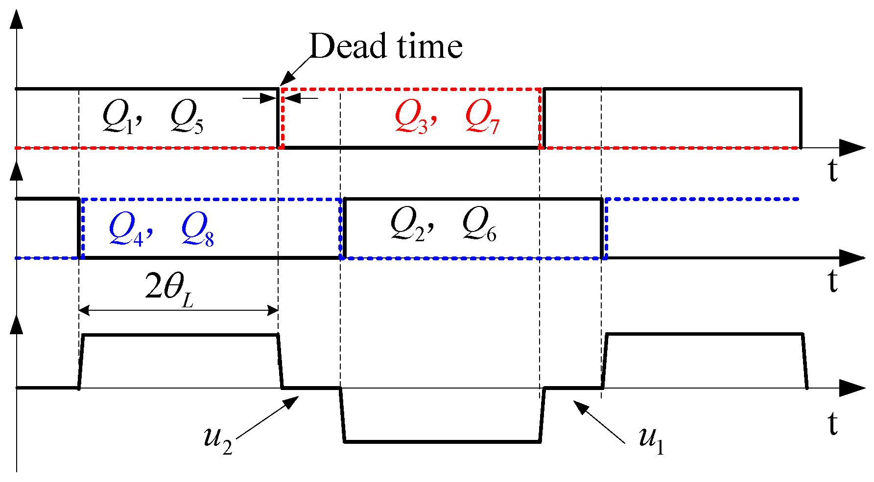
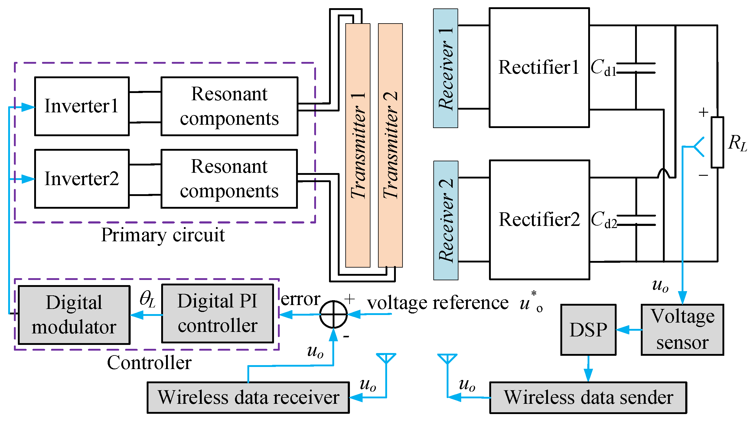
3.4. Control Diagram

Conventionally, the output voltage powering the load should be constant in various applications. For the proposed WPT system, in order to regulate output voltage of the load at its designed value, a linear feedback controller is designed which is given in Figure 8. The output voltage of the load is detected by a voltage sensor, and the voltage date is processed by a digital signal processor (DSP). Then, a wireless signal communication module (NRF24L01+) [35] is adopted to send the measured output voltage (uo) of the load to the primary controller for the closed-loop control. The primary controller can be in form of Proportional-Integral (PI) or Proportional (P) controllers, etc. In this paper, a digital PI controller is adopted to control the output voltage. The controller controls and regulates the amplitude of output voltage (uo) by altering the inverter conduction angle θL shown in Figure 5. The output voltage reference is set to be u*o. Assuming that a perturbation occurs in uo, e.g., uo > u*o, the output of the controller θL should decrease. Consequently, uo can be controlled to be the reference voltage u*o. It should be noted that the output voltage can be maintained even with faulty inverter and rectifier owe to the redundant magnetic structure with four energy transmission paths.

4. Experimental Verification

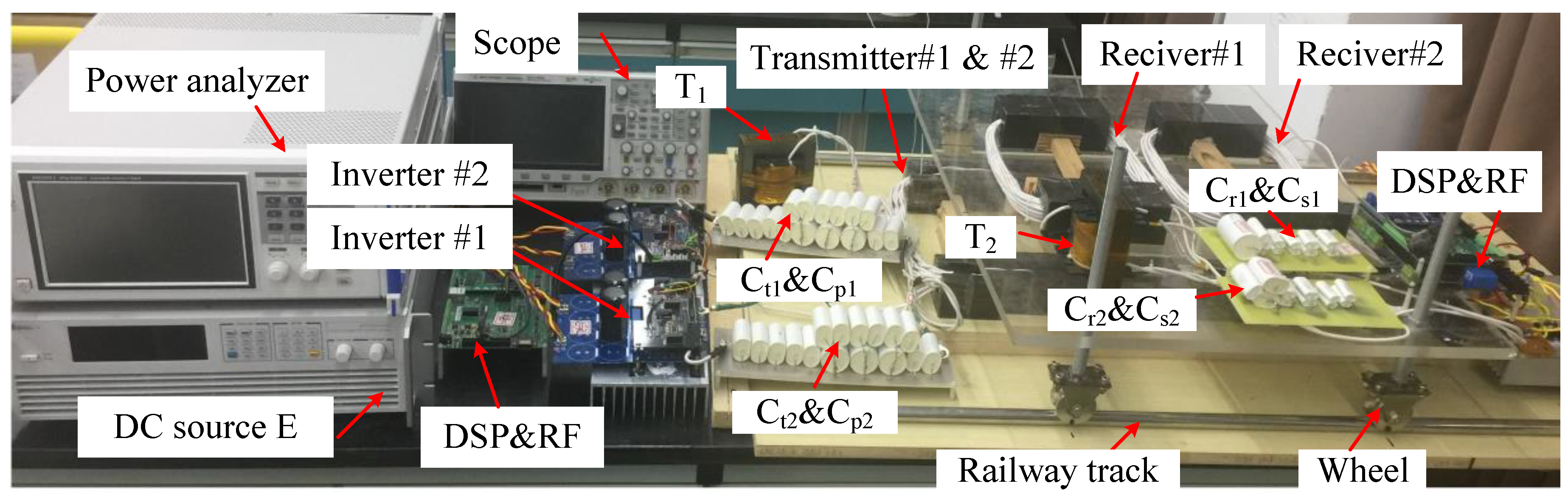
4.1. Prototype System

In order to verify the proposed approach, an experimental WPT prototype, comprising two transmitters, two resonant inverters and two receivers, was built in the laboratory settings. The laboratory setup is shown in Figure 9. The sizes of the coils are designed according to the FEA simulation results. The mutual inductances and self-inductances of the transmitters and receiver are measured by an E4980A LCR meter (Agilent, Palo Alto, CA, USA). The specifications of the experimental setup are listed in Table 1. The inverters’ operating frequency is 40 kHz. An electronic load is adopted as the load connected with the rectifiers. A PW6001 power analyzer from HIOKI (Nagano, Japan) is connected with the system to calculate the overall efficiency by measuring the input power from the inverters and the output power to the electronic load.

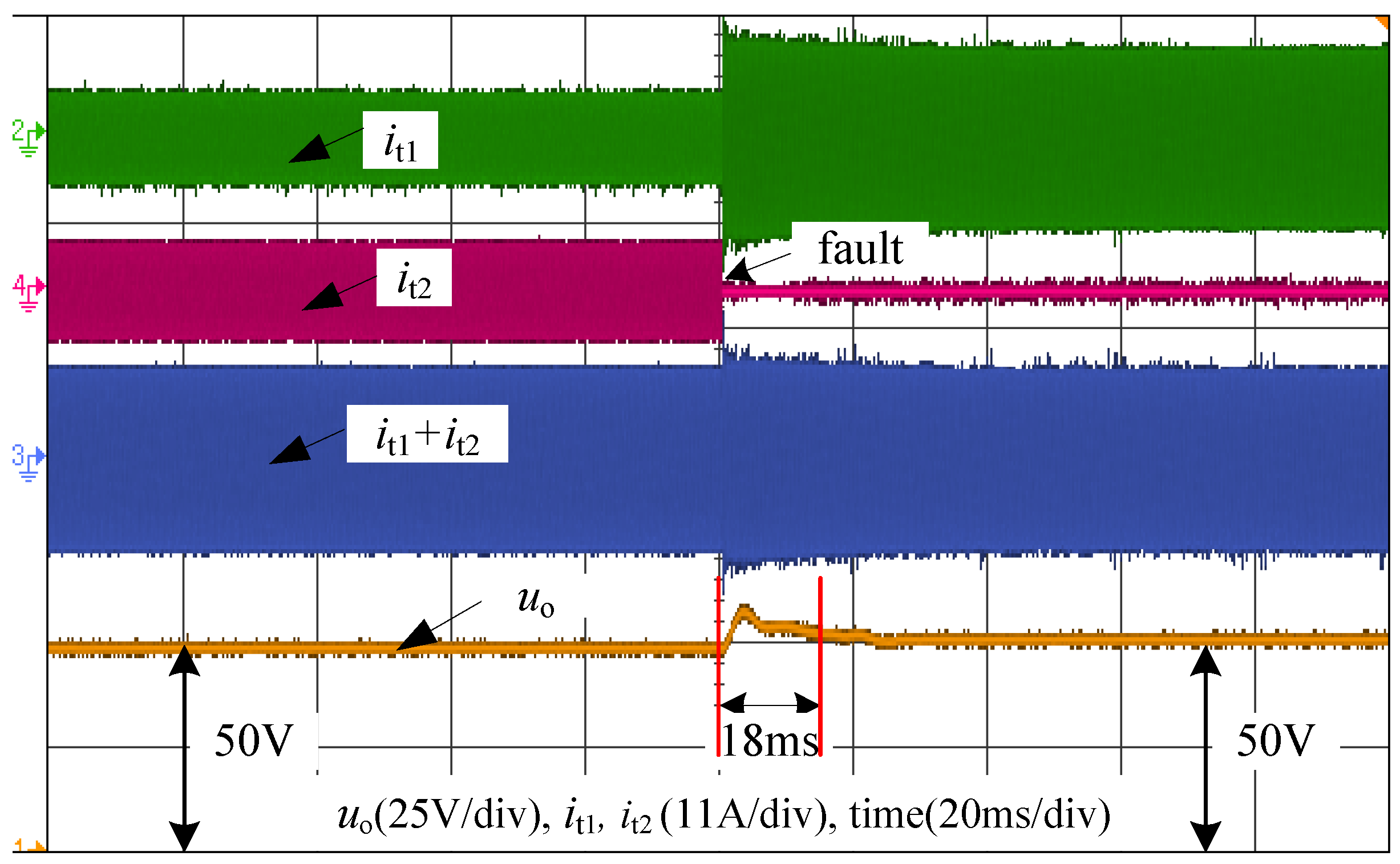
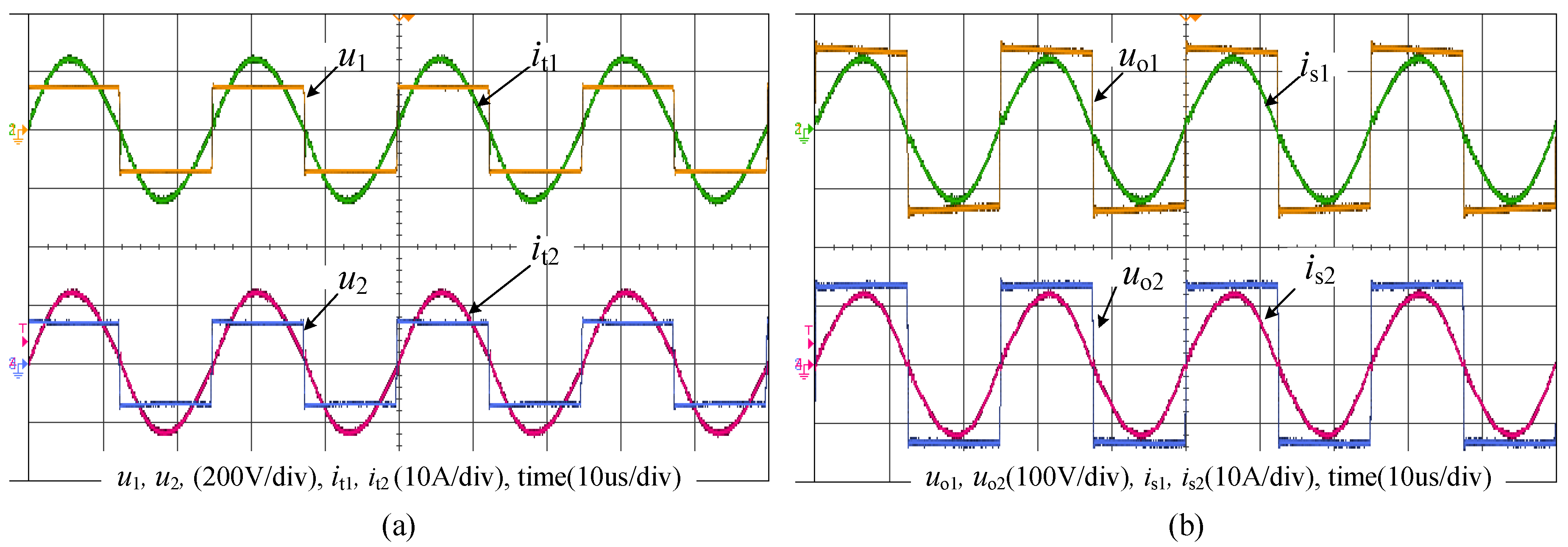
4.2. Experimental Results

According to Equation (17), the optimal load is calculated to be about 8 Ω. The peak overall efficiency (DC-DC efficiency) can be achieved at 93.62% when the system delivers 2.1 kW to the optimal load, and the waveforms of the primary-side and secondary-side are shown in Figure 10. The inverters can achieve unity power factor with the proposed decoupling transformers, which only provide the active powers to the load. The measured peak overall efficiency is shown in Figure 11, where P1 and P2 are the input power of two inverters and the total input power is Pin, P3 and P4 are the output power of the rectifiers and the total output power is Po. As can be seen form Figure 11, both transmitters and receivers can achieve power sharing and the transmitted power can be enhanced by the proposed structure. Besides, the overall power loss (Ploss) is about 144 W, and the measured power loss distribution is shown in Figure 11. The extra decoupling transformers only bring 6.8 W power loss by using litz wire, which can be negligible compared to 2.1 kW. The overall efficiencies with various loads for the WPT system are shown in Figure 12. As expected, the efficiency increases significantly with decoupling transformers compared to that without these, especially for heavy-load conditions.
It is necessary to investigate the dynamic performances of the proposed control method. Figure 13 shows the output voltage waveform, the current waveforms of the two transmitters. The output voltage decreases from 100 V to 80 V with a fast transient of 10 ms following the changes in the reference signal, and raises from 80 V back to 100 V with a very fast response time of 8 ms without overshoot. Therefore, the output voltage can be tightly controlled by the proposed control method.
In order to evaluate the reliability of the proposed WPT system, it is desirable to investigate the performance of the system with a fault. The transient waveforms of the experimental setup when inverter unit #2 occurs a fault as shown in Figure 14. The output voltage is supposed to be regulated to 50 V during normal operation. With the occurrence of a fault in one of the inverters, the output voltage can be maintained to be 50 V with a fast response time of 18 ms and with a slight transient overshoot by increasing the output power of inverter unit #1. Although the transmitter current it2 decreases to zero, the load cannot feel any change from the power source and the system keeps working continuously, which proves the availability and reliability of the proposed method. The whole system can still work, and it is clear that the proposed WPT system is more reliable than traditional one.

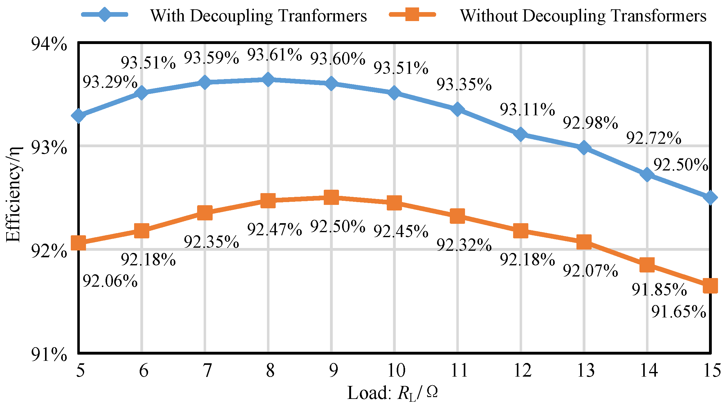
5. Discussion and Comparison with Traditional WPT Systems

The proposed WPT system is compared with the traditional WPT system with one transmitter and one receiver as follows. For low power applications such as 2 kW requirement, it is easy and economical to realize a WPT system with traditional one transmitter and one receiver other than the proposed structure. However, the traditional WPT system only have one energy transmission path, which results in a low reliability. Moreover, in some practical applications, the installation space for receiver is limited by the available space of the bottom of the vehicle. A small size receiver coil will result in a low coupling coefficient and a limitation for the output power of the WPT system. However, the traditional WPT system may not meet the requirements of some high power applications. Our research goal is to use multiple relative “lower” power inverters and receivers to achieve high power output as required by some high applications. With the proposed structure, the WPT system can achieve a high reliability because of the availability of the four energy transmission paths. Moreover, the inverters and rectifiers can be designed and manufactured in large quantities to reduce the manufacturing cost, because redesigning and manufacturing an inverter is usually a time-consuming and expensive process. Therefore, the proposed WPT system can achieve better performance than the traditional WPT system.
However, due to the limitation of our experiment condition, this paper only theoretically and experimentally proves the 2.1 kW output power effectiveness by using two 1.1 kW resonant inverters composed of low capacity semiconductors. The proposed method in this paper has potential advantages for higher power level applications. Future research will focus on system optimization and implementation to increase power level and efficiency. Moreover, the proposed structure can be easily extended to the applications with multiple transmitters and multiple receivers.

6. Conclusions

In order to improve the power capacity of the WPT system for high power applications, a dual transmitter and dual receiver-based WPT topology by using lower cost and power rating semiconductors is proposed. The reliability and availability of the proposed WPT system can be dramatically improved by the proposed structure due to the four transmission paths. The characteristics of the proposed magnetic coupling structure are investigated by FEA. Decoupling transformers are utilized to decouple the cross coupling between the transmitters and receivers, which can improve the overall efficiency and reduce reactive power of the inverters. Besides, the output voltage in the secondary side can be regulated at its designed value with a fast response performance. The proposed structure and corresponding approach are verified through a scale-down experimental setup in university laboratory. Besides, the overall system efficiency is improved to 93.62% with the decoupling transformers at 2.1 kW output power.

Acknowledgments

This work is supported by National Natural Science Foundation of China (51507147), the National Science Fund for Distinguished Young Scholars (51525702), the National Natural Science Foundation of China under Grant (No. 51677155), Independent Research Subject of the State Key Laboratory of Traction Power (2016TPL_T11), the 2016 Doctoral Innovation Funds of Southwest Jiaotong University and Scientific Talent Engineering Breeding Project of Sichuan Province (No. 2016117).

Author Contributions

Yong Li and Tianren Lin conceived and designed the experiments; Tianren Lin performed the experiments; Yong Li and Ruikun Mai analyzed the data; all authors contributed to the writing of the manuscript, and have read and approved the final manuscript.

Conflicts of Interest

The authors declare no conflict of interest.

References

  1. Graham, D.J.; Neasham, J.A.; Sharif, B.S. Investigation of methods for data communication and power delivery through metals. IEEE Trans. Ind. Electron. 2011, 58, 4972–4980. [Google Scholar] [CrossRef]
  2. Moorey, C.; Holderbaum, W.; Potter, B. Investigation of High-Efficiency Wireless Power Transfer Criteria of Resonantly-Coupled Loops and Dipoles through Analysis of the Figure of Merit. Energies 2015, 8, 11342–11362. [Google Scholar] [CrossRef]
  3. Amini, M.R.; Farzanehfard, H. Three-phase soft-switching inverter with minimum components. IEEE Trans. Ind. Electron. 2011, 58, 2258–2264. [Google Scholar] [CrossRef]
  4. Li, Y.L.; Sun, Y.; Dai, X. μ-Synthesis for Frequency Uncertainty of the ICPT System. IEEE Trans. Ind. Electron. 2013, 60, 291–300. [Google Scholar] [CrossRef]
  5. Joun, G.B.; Cho, B.H. An energy transmission system for an artificial heart using leakage inductance compensation of transcutaneous transformer. IEEE Trans. Power Electron. 1998, 13, 1013–1022. [Google Scholar] [CrossRef]
  6. Si, P.; Hu, A.P.; Malpas, S. A frequency control method for regulating wireless power to implantable devices. IEEE Trans. Biomed. Circuits Syst. 2008, 2, 22–29. [Google Scholar] [CrossRef] [PubMed]
  7. Klontz, K.W.; Divan, D.M.; Novotny, D.W. Contactless power delivery system for mining applications. IEEE Trans. Ind. Appl. 1995, 31, 27–35. [Google Scholar] [CrossRef]
  8. Kuipers, J.; Bruning, H.; Bakker, S. Near field resonant inductive coupling to power electronic devices dispersed in water. Sens. Actuators A Phys. 2012, 178, 217–222. [Google Scholar] [CrossRef]
  9. Hasanzadeh, S.; Vaez-Zadeh, S.; Isfahani, A.H. Optimization of a contactless power transfer system for electric vehicles. IEEE Trans. Veh. Technol. 2012, 61, 3566–3573. [Google Scholar] [CrossRef]
  10. Zhong, W.X.; Zhang, C.; Liu, X. A methodology for making a three-coil wireless power transfer system more energy efficient than a two-coil counterpart for extended transfer distance. IEEE Trans. Power Electron. 2015, 30, 933–942. [Google Scholar] [CrossRef]
  11. Smeets, J.P.C.; Overboom, T.T.; Jansen, J.W. Comparison of position-independent contactless energy transfer systems. IEEE Trans. Power Electron. 2013, 28, 2059–2067. [Google Scholar] [CrossRef]
  12. Elliott, G.A.J.; Raabe, S.; Covic, G.A. Multiphase pickups for large lateral tolerance contactless power-transfer systems. IEEE Trans. Ind. Electron. 2010, 57, 1590–1598. [Google Scholar] [CrossRef]
  13. Huh, J.; Lee, S.W.; Lee, W.Y. Narrow-width inductive power transfer system for online electrical vehicles. IEEE Trans. Power Electron. 2011, 26, 3666–3679. [Google Scholar] [CrossRef]
  14. Kim, J.; Lee, B.; Lee, J.; Lee, S.; Park, C.; Jung, S.; Lee, S.; Yi, K.; Baek, J. Development of 1 MW Inductive Power Transfer System for a High Speed Train. IEEE Trans. Ind. Electron. 2015, 62, 6242–6250. [Google Scholar] [CrossRef]
  15. Li, Y.; Mai, R.; Yang, M.; He, Z. Cascaded Multi-Level Inverter Based IPT Systems for High Power Applications. J. Power Electron. 2015, 15, 1508–1516. [Google Scholar] [CrossRef]
  16. Hao, H.; Covic, G.A.; Boys, J.T. A parallel topology for inductive power transfer power supplies. IEEE Trans. Power Electron. 2014, 29, 1140–1151. [Google Scholar] [CrossRef]
  17. Li, Y.; Mai, R.K.; Lu, L.W.; He, Z.Y. Active and Reactive Currents Decomposition based Control of Angle and Magnitude of Current for a Parallel Multi-Inverter IPT System. IEEE Trans. Power Electron. 2017, 32, 1602–1614. [Google Scholar] [CrossRef]
  18. Johari, R.; Krogmeier, J.V.; Love, D.J. Analysis and practical considerations in implementing multiple transmitters for wireless power transfer via coupled magnetic resonance. IEEE Trans. Ind. Electron. 2014, 61, 1774–1783. [Google Scholar] [CrossRef]
  19. Ahn, D.; Hong, S. Effect of coupling between multiple transmitters or multiple receivers on wireless power transfer. IEEE Trans. Ind. Electron. 2013, 60, 2602–2613. [Google Scholar] [CrossRef]
  20. Li, Y.; Mai, R.; Lu, L.; He, Z. A Novel IPT System Based on Dual Coupled Primary Tracks for High Power Applications. J. Power Electron. 2016, 16, 111–120. [Google Scholar] [CrossRef]
  21. Yoon, I.J.; Ling, H. Investigation of Near-Field Wireless Power Transfer under Multiple Transmitters. IEEE Antennas Wirel. Propag. Lett. 2011, 10, 662–665. [Google Scholar] [CrossRef]
  22. Nguyen, C.M.; Kota, P.K.; Nguyen, M.Q.; Dubey, S.; Rao, S.; Mays, J.; Chiao, J.C. Wireless Power Transfer for Autonomous Wearable Neurotransmitter Sensors. Sensors 2015, 15, 24553–24572. [Google Scholar] [CrossRef] [PubMed]
  23. Rajagopal, S.; Khan, F. Multiple Receiver Support for Magnetic Resonance Based Wireless Charging. In Proceedings of the IEEE International Conference on Communications Workshops, Tokyo, Japan, 5–9 June 2011; pp. 1–5.
  24. Cannon, B.L.; Hoburg, J.F.; Stancil, D.D.; Goldstein, S.C. Magnetic Resonant Coupling as a Potential Means for Wireless Power Transfer to Multiple Small Receivers. IEEE Trans. Power Electron. 2009, 24, 1819–1825. [Google Scholar] [CrossRef]
  25. Imura, T.; Hori, Y. Optimization using transmitting circuit of multiple receiving antennas for wireless power transfer via magnetic resonance coupling. In Proceedings of the Telecommunications Energy Conference, Amsterdam, The Netherlands, 9–13 October 2011; Volume 47, pp. 1–4.
  26. Nguyen, H.; Agbinya, J.I.; Devlin, J. FPGA-based implementation of multiple modes in near field inductive communication using frequency splitting and MIMO configuration. IEEE Trans. Circuits Syst. I Regul. Pap. 2015, 62, 302–310. [Google Scholar] [CrossRef]
  27. Madawala, U.K.; Thrimawithana, D.J. Modular-based inductive power transfer system for high-power applications. IET Power Electron. 2012, 5, 1119–1126. [Google Scholar] [CrossRef]
  28. Zhen, N.L.; Casanova, J.J.; Lin, J. A Loosely Coupled Planar Wireless Power Transfer System Supporting Multiple Receivers. IEEE Trans. Ind. Electron. 2009, 56, 3060–3068. [Google Scholar]
  29. Li, X.; Zhang, H.; Peng, F.; Li, Y.; Yang, T.; Wang, B.; Fang, D. A Wireless Magnetic Resonance Energy Transfer System for Micro Implantable Medical Sensors. Sensors 2012, 12, 10292–10308. [Google Scholar] [CrossRef] [PubMed]
  30. Kim, J.W.; Son, H.C.; Kim, D.H.; Yang, J.R.; Kim, K.H.; Lee, K.M.; Park, Y.J. Wireless power transfer for free positioning using compact planar multiple self-resonators. In Proceedings of the Microwave Workshop Series on Innovative Wireless Power Transmission: Technologies, Systems, and Applications, Tokyo, Japan, 10–11 May 2012; pp. 127–130.
  31. Kim, J.; Son, H.C.; Kim, D.H.; Park, Y.J. Optimal design of a wireless power transfer system with multiple self-resonators for an LED TV. IEEE Trans. Consum. Electron. 2012, 58, 775–780. [Google Scholar] [CrossRef]
  32. Song, Y.; Madawala, U.K.; Hu, A.P. Cross coupling effects of poly-phase bi-directional inductive power transfer systems used for EV charging. In Proceedings of the Future Energy Electronics Conference (IFEEC), Taipei, Taiwan, 1–4 November 2015; pp. 1–7.
  33. Kissin, M.L.G.; Boys, J.T.; Covic, G.A. Interphase mutual inductance in polyphase inductive power transfer systems. IEEE Trans. Ind. Electron. 2009, 56, 2393–2400. [Google Scholar] [CrossRef]
  34. Choi, S.Y.; Jeong, S.Y.; Lee, E.S.; Gu, B.W.; Lee, S.W.; Rim, C.T. Generalized models on self-decoupled dual pick-up coils for large lateral tolerance. IEEE Trans. Power Electron. 2015, 30, 6434–6445. [Google Scholar] [CrossRef]
  35. Nordic Semiconductor. nRF24L01+ Datasheet. 2013. Available online: http://www.nordicsemi.com/eng/Products/2.4GHz-RF/nRF24L01P (accessed on 14 October 2016).
Figure 1. The structure of the proposed WPT system.
Energies 10 00174 g001
Figure 2. Cross couplings among the coils.
Energies 10 00174 g002
Figure 3. Inductance variations with misalignments: (a) inductances of the coils with x-axis misalignment; (b) mutual inductances of the coils with x-axis misalignment; (c) inductances of the coils with y-axis misalignment; (d) mutual inductances of the coils with y-axis misalignment.
Energies 10 00174 g003
Figure 4. The circuit of proposed WPT system.
Energies 10 00174 g004
Figure 5. Principal operation waveforms of inverter 1 and inverter 2.
Energies 10 00174 g005
Figure 6. The circuit of proposed WPT system with decoupling transformers.
Energies 10 00174 g006
Figure 7. Decoupled transformers: (a) the model established in MAXWELL; (b) Magnetic field distribution.
Energies 10 00174 g007
Figure 8. Control diagram of the proposed WPT system.
Energies 10 00174 g008
Figure 9. Laboratory setup.
Energies 10 00174 g009
Figure 10. Experimental results: (a) waveforms of primary inverters output; (b) waveforms of secondary rectifiers input.
Energies 10 00174 g010
Figure 11. Optimal efficiency results: (a) capture of the power analyzer; (b) power loss distribution.
Energies 10 00174 g011
Figure 12. Measured overall efficiencies with various loads.
Energies 10 00174 g012
Figure 13. Dynamic tracking performance: (a) from 100 V to 80 V; (b) from 80 V to 100 V.
Energies 10 00174 g013
Figure 14. Transient waveforms of the experimental system when inverter #2 is shut down.
Energies 10 00174 g014
Table 1. Specifications and circuit parameters of WPT prototype.
SymbolValueSymbolValue
Lt1143.50 μHCt1110.32 nF
Lt2143.45 μHCt2110.36 nF
Lr1225.8 μHCr170.11 nF
Lr2226.3 μHCr269.96 nF
Lp1182.22 μHCp186.88 nF
Lp2183.42 μHCp286.31 nF
Ls160.23 μHCs1262.84 nF
Ls260.75 μHCs2260.60 nF
Mt136.5 μHMp136.6 μH
Mr15.9 μHMs15.9 μH
Rt0.12 ΩRr0.09 Ω
M26.3 μH--

