1. Introduction
In the last years, there is an increasing demand for power devices able to tolerate very high radiation levels [
1,
2,
3]. This is particularly relevant in the field of High Energy Physics (HEP) [
4] experiments, where a large spectrum of power devices and systems are required to operate the particle accelerator machines and the particle detectors. In those applications, the electronics is expected to withstand extremely harsh radiation fields and, in some cases, such as the future upgrade for High-Luminosity of the Large Hadron Colider (HL-LHC) at European Organization for Nuclear Research (CERN), in Geneva (Switzerland), with an unprecedented level of radiation [
5,
6]. Among the large variety of power electronics applications in such a huge experiment, the sensor biasing circuitry [
7] requires high voltage but not high current, since they consist of reverse biased diodes, with typical leakage currents below the order of microamperes before being irradiated [
8]. Although the current demand increases to the milliampere range after irradiation, the challenging factor for the associated electronics is typically related with the voltage demand (up to 1000 V), and the performance degradation due to the high radiation level.
A careful search for suitable power switches is mandatory for reliable operation of the final application. Wide bandgap semiconductors, such as GaN or SiC, may offer good performance in some specific cases [
9]. Vertical JFET SiC devices with voltage capability up to 1700 V have been successfully fabricated and tested in harsh conditions [
10,
11]. Although these devices integrated on SiC substrates a better than Silicon counterparts in terms of ionization hardness due to the wider bandgap, suffer from performance degradation due to displacement damage, similar to that of Silicon devices. In this contest, solutions based on Silicon technology are still preferred, because the maturity of this technology is crucial to design and fabricate power devices that have to be fully operative and not accessible during several years, when the experiment is in operation. Besides, radiation effects in Silicon technologies have been studied for years, and the subsequent performance degradation on the electronic devices is well understood and predictable to a greater extent. Among the high voltage Silicon power devices, those based on MOS technology (Metal Oxide Semiconductor Field Effect Transistor, MOSFET, and Insulated Gate Bipolar Transistor, IGBTs) are very sensitive to ionizing radiation [
12,
13] although new designs are continuously produced to improve the radiation hardness [
14]. Thyristors are current controlled devices with two low-doped regions (p- and n-type). Although these devices are harder in terms of ionization damage, the fast degradation of the low-doped regions because of the non-ionizing radiation [
15] make not advisable their use.
In this context, the IMB-CNM has proposed a new Vertical JFET (V-JFET) transistor based on a 3D deep trenched technology [
16] implemented on p-type substrates to minimize the displacement damage at high radiation fluences.
2. Device Structure
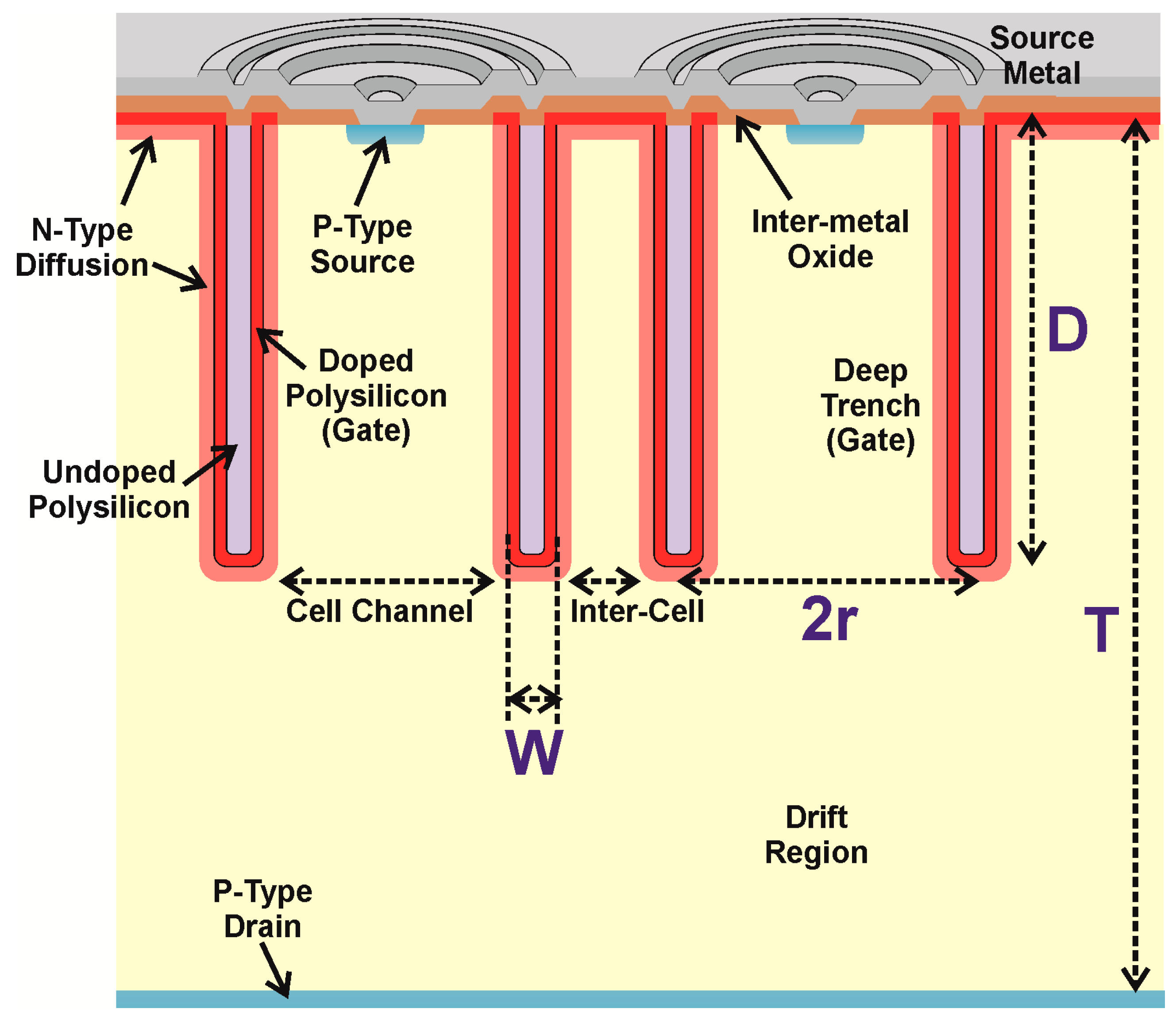
The proposed V-JFET power device has a highly adaptable design, which allows the transistor to exhibit very different performance depending on the values of the relevant geometrical parameters. The active area of the device is arranged with a large number of paralleled cells with vertical conduction. The channel is confined by a ring-shaped trench, deeply etched into the silicon substrate. As shown in
Figure 1, where a schematic cross section through the center of two basic cells is depicted, the trenches are filled with highly doped polysilicon to work as the Gate electrode. A Source electrode is placed on the channel surface at the center of each cell, and then connected to the Source metal. Drain electrode is placed at the opposite face of the substrate. The trenches are all connected to the same polysilicon layer, which is then reached elsewhere by a metal pad, well isolated from the Source metal to avoid short-circuit among the electrodes.
In order to gain structural stability and to attain well filling and sealing of the trenches, a ring-shaped layout with a certain separation among adjacent cells was preferred. Other arrangements, missing cell-to-cell separation or even considering hexagonal cells, turned out unsuitable [
17], since many of the channels collapsed and the trenches were not satisfactorily filled. In this sense, the characteristic width uniformity in the trenches of the ring-shaped layout helps to improve the filling process. In addition, a second polysilicon layer (undoped) is included to refill the trenches, thus ensuring a complete sealing. The separation between adjacent cells does not deteriorate the connection of the cells to a common Gate, since the doped polysilicon layer is not interrupted. Besides, the diffusion of the n-type dopant impurities from the polysilicon into the p-type substrate contributes to interconnect the Gates of the individual cells.
From the electrical point of view, the V-JFET is a depletion mode transistor, with channel conduction at zero Gate-to-Source bias (
VGS). Each cell acts as an individual JFET transistor, with vertical conduction and switching properties very close to the pentode characteristics expected for an ideal long-channel JFET [
18]. Thanks to the deeply etched Gate surrounding the silicon channel, the conduction is mainly controlled by the Gate voltage and a relatively high current level can be obtained for low Drain voltages (
VDS), whereas for higher
VDS values a current saturation is observed. The proposed structure is switched-off at low
VGS values due to the fast depletion of the narrow channels of the individual cells. Besides, the long distance that separates the drain electrode from the bottom of the trenches, the so-called drift region in
Figure 1, provides the high voltage capability of the cell, at the cost of adding a series resistance to the conduction channel. Although a single cell is not able to drive a large amount of current, the additive effect of the parallel cell arrangement hugely expands the total current handling capability.
The performance of the V-JFET transistor strongly depends on several geometrical and technological parameters. Among them, the trench depth (D), the cell radius (r), and the substrate doping concentration (NA) have been identified as the more relevant for finding an optimum design. Other important parameters, such as the trench width (W) and the substrate thickness (T), are fixed or limited by technological constrains. Finally, the desired active area of the device (A) determines the number of basic cells connected in parallel and the resulting current handling capability of the V-JFET transistor.
The electrical performance and the process technology of the proposed transistor has been extensively simulated with the aid of Sentaurus TCAD software (Synopsys Inc., Mountain View, CA, USA), using the physical models typical from power devices. The dependence on the trench depth is illustrated in
Figure 2, where the switch-off voltage (
VOFF) and breakdown voltage (
VBD|CELL) of an individual cell within the arrangement (a so-called “inner cell”) are represented as a function of
D. Deep trenches are generally preferred to obtain pentode-like characteristics. However, as
D is increased, the drift region becomes shorter and
VBD|CELL decreases. For any inner cell, the highest voltage capability is achieved at the lowest
D value, when the performance approaches the triode-like characteristics [
16]. Nevertheless, the strongest influence of the Drain potential in such a short-channel transistor would increase the Gate voltage required to deplete the cell, leading to a drastic increase of the
VOFF value. Considering a substrate thickness of
T = 300 µm, the optimum
D value ranges between 60 and 100 µm.
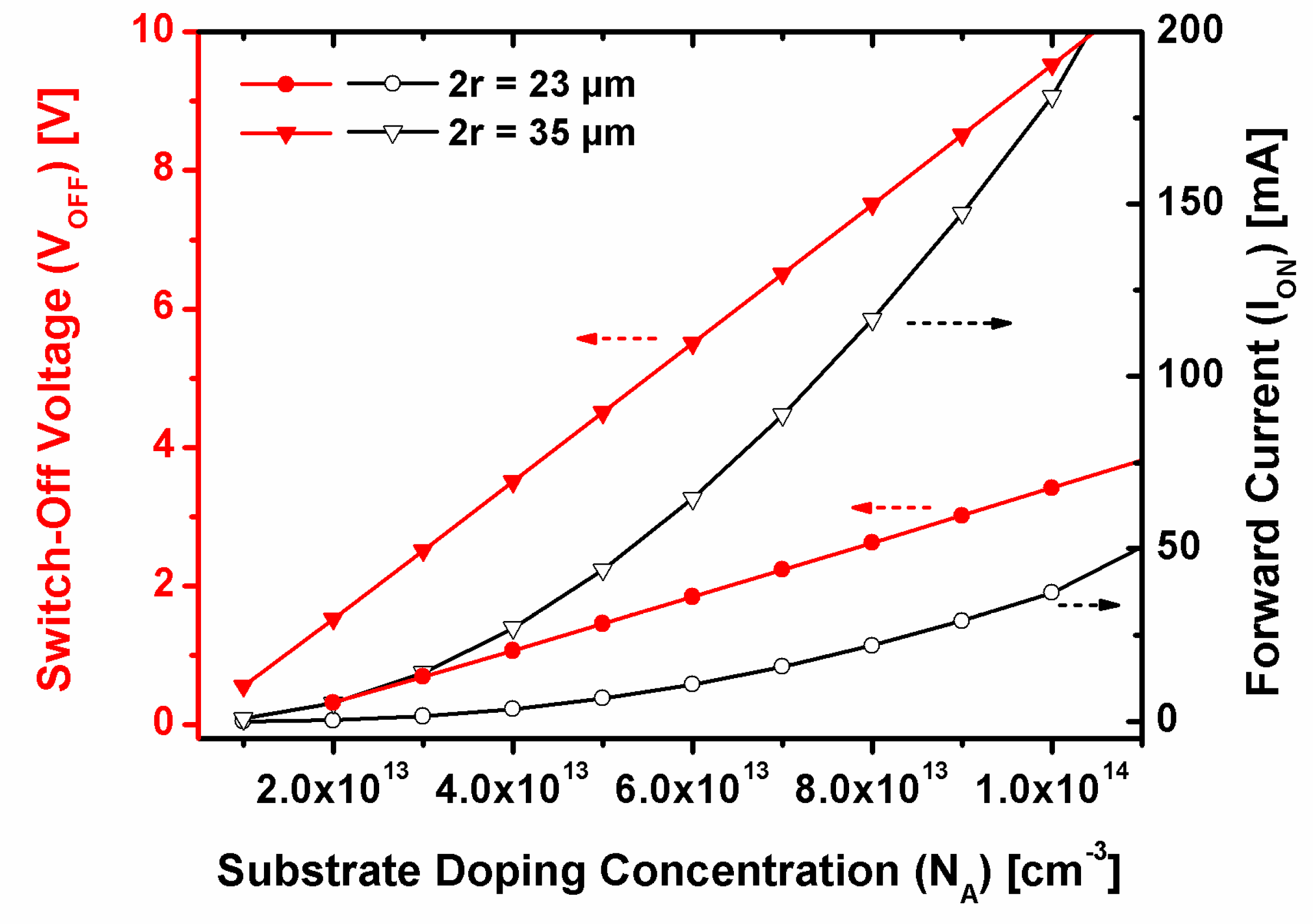
Dependences on r and
NA are more directly correlated. In general, higher current levels can be obtained for higher
NA values, although this is strongly modulated by
r, since the wider is the cell channel, the higher is the current handling capability. This is in contrast with the switching performance, because low
NA and
r values are required to deplete the cell channel at low voltage values. The switching versus current capability trade-off is illustrated in
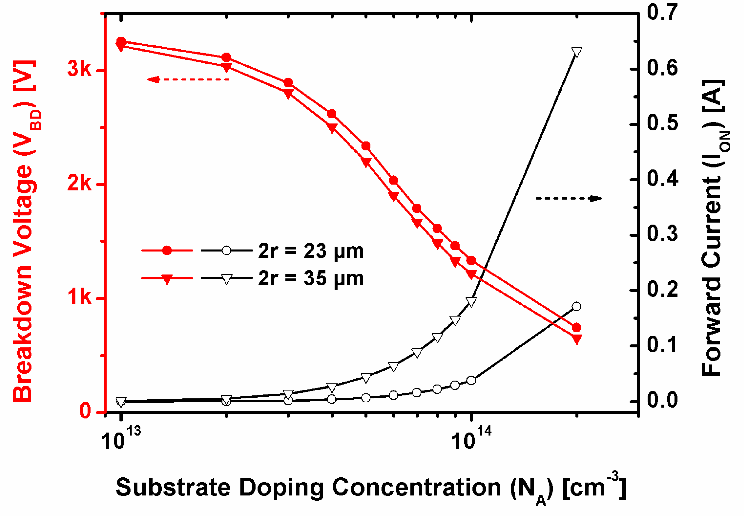
Figure 3, where
VOFF and the forward current value at saturation (
ION) are represented as a function of
NA, for two different channel diameters (2
r = 23 and 35 µm) in a V-JFET transistor with
A = 5 × 5 mm
2. In this example, a convenient
VOFF = 3 V can be easily obtained for the 2
r = 23 µm transistor as long as
NA is lower than 1 × 10
14 at/cm
3. Still,
ION will be always below 30 mA. The current level can be significantly increased if the 2
r = 35 µm design is considered, although for
NA = 1 × 10
14 at/cm
3,
VOFF will increase up to almost 10 V. To regain the previous V
OFF value of 3 V,
NA should be reduced below 4 × 10
13 at/cm
3, with the consequent
ION reduction.
VOFF is the major limiting factor, since control electronics with low switching voltage is generally preferred. Hence, low
r and
NA values are favored. On the other hand, the current handling capability depends also on the total number of parallel cells, i.e., on
A. Therefore, if the optimum
r and
NA values for attaining low
VOFF lead to too low
ION value, a layout with broader
A can be considered to achieve the desired current level. Moreover, a device optimization based on
NA is somewhat cumbersome, since working with high resistivity substrates implies low accuracy in their doping level. Higher precision could be achieved by increasing
NA, and this would also produce a remarkable increase of the current handling capability, but the voltage capability will be drastically worsened. This is illustrated in
Figure 4, where
VBD|CELL and
ION have been represented as a function of
NA. It can be clearly seen that the current capability increases with the cell diameter and the substrate doping concentration. On the contrary, the cell diameter has no relevant effect on the
VBD|CELL value, which is basically determined by the substrate doping concentration. This is a direct consequence of the self-protection between adjacent trenches that moves the weakest point to the last cell of the device. On the whole, if for instance a final
A = 5 × 5 mm
2 transistor with
VOFF < 3 V, I
ON ranging between 10 and 100 mA, and
VBD|CELL > 1000 V is desired,
NA should range between 2 and 8 × 10
13 at/cm
3, whereas the optimum cell diameter is valued between 2
r = 20 and 35 µm.
Besides on the features of an optimized active region, the final performance of the V-JFET transistor rests on the suitability of the edge termination design. In contrast with the inner cells, the cells placed at the periphery of the active region show an asymmetric distribution of the electrostatic potential. As a result, the breakdown voltage of these outer cells is significantly lower than VBD|CELL, unless a proper termination is implemented. The design of the edge termination region is challenging, as the maximum electric field value is located at the bottom of the trenches, typically ~100 µm far from the silicon surface. Additionally, a gate runner, consisting of a peripheral n-type diffusion connected to the Gate electrode with a maximum doping concentration in the range of 1 × 1018 cm-3, has been placed around the whole active area to ensure uniform Gate bias distribution to all the cells in the layout. Gate runners are always used in the large area power devices with multi-cellular layout, also including the peripheral gate runner. This design approach has been followed in the new V-JFET structure proposed in this paper. The n-type diffusion is placed below the whole gate runner area to avoid premature breakdown as a consequence of the non-uniform cell distribution at the device periphery. Although several technologically elaborated designs are still under study, for the first fabrication batch, a planar solution with 4 floating guard rings has been chosen. This conservative approach allows the full transistor to achieve a useful voltage capability (VBD|FULL) of several hundreds of volts, though always lower than VBD|CELL.
3. Technological Process
The fabrication of the V-JFET transistors at the IMB-CNM clean room includes more than 90 technological steps, 7 photolithographic mask levels and several ion implantation processes at different doses of Boron, Phosphorus, and Arsenic dopants. Besides, the use of a highly doped polysilicon layer for defining the Gate electrode allows the utilization of just a single additional metal layer to interconnect the Source electrodes of the cells. Among the different steps, two key operations are of major concern: the trench etching and the trench complete sealing. The trenches are etched by means of a deep reactive ion etching (DRIE) technique [
19], which gives excellent verticality and uniformity in trenches even more than 200 µm deep. A complete sealing is then required for structural stability and to permit the following steps of the process (photolithography and layer depositions). Two polysilicon layers are successively deposited to this aim. The first one is doped in a POCl
3 ambient immediately after the deposition, to acquire the n-type character required to work as the gate electrode. A second polysilicon layer is then deposited to refill the trench. This second undoped layer is then completely removed from the surface, since it does not play any role in the front-end connections. As seen from SEM images, the trench is not fully filled by the undoped polysilicon since the deposition method causes a premature trench sealing, which is mandatory to continue with the subsequent technological steps. Nevertheless, the incomplete trench filling does not have any relevant impact on the current and voltage capabilities. Before the metal deposition, a thick inter-level oxide layer is deposited to get the required isolation between the Gate and Source electrodes. A BPTEOS oxide of 730 nm is preferred for its good quality and excellent replication of the surface topography. The device is finished with the source and drain metals (Al/Cu of 1.5 and 1 µm, respectively) and the passivation layer consisting of consecutively deposited oxide and nitride layers with a total thickness of 700 nm. The active area of the fabricated devices is fixed at 5 × 5 mm
2 but the number of paralleled cells depends on the 2
r value: 9.500 for 2
r = 35 µm and 14.000 for 2
r = 23 µm.
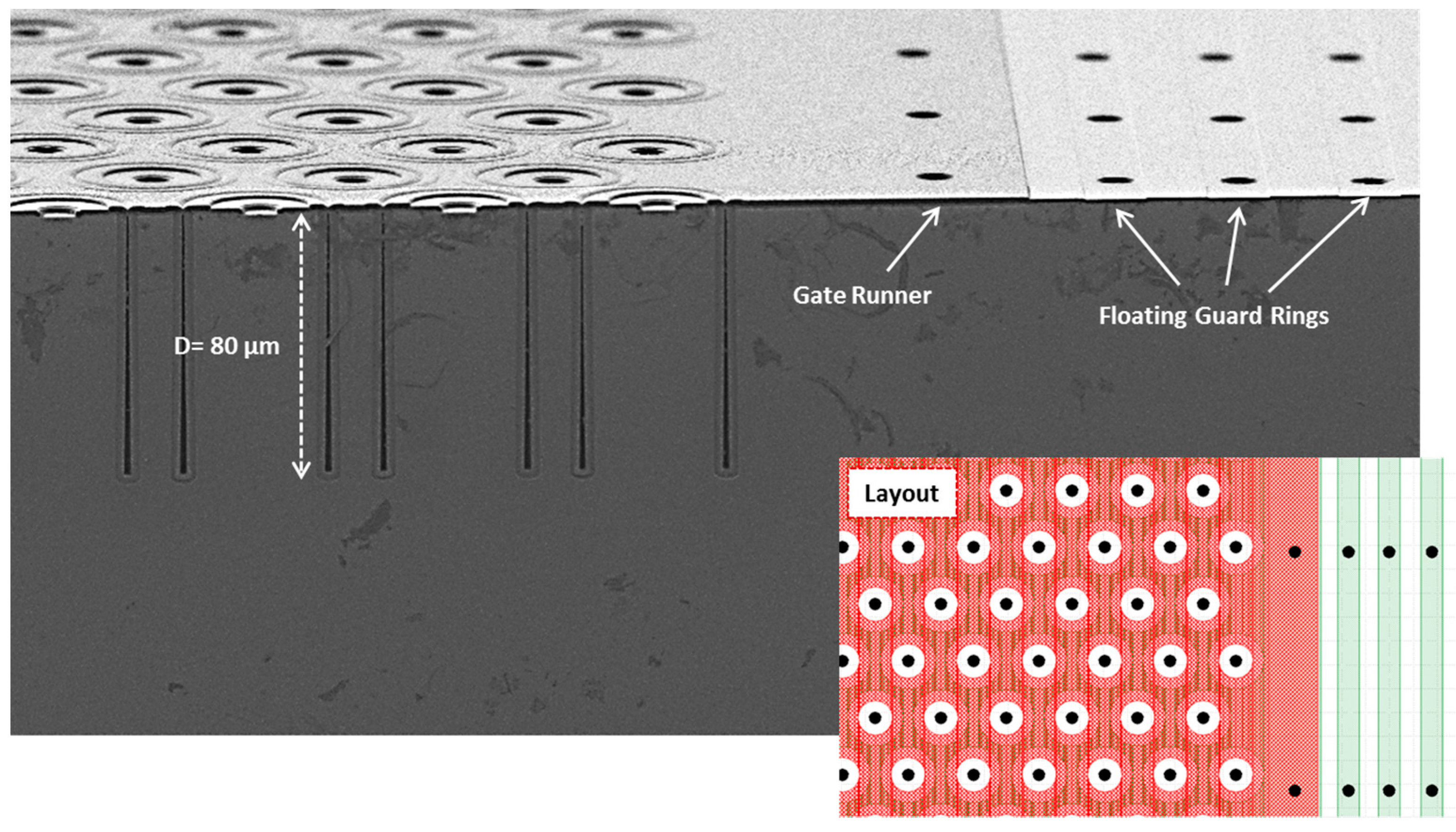
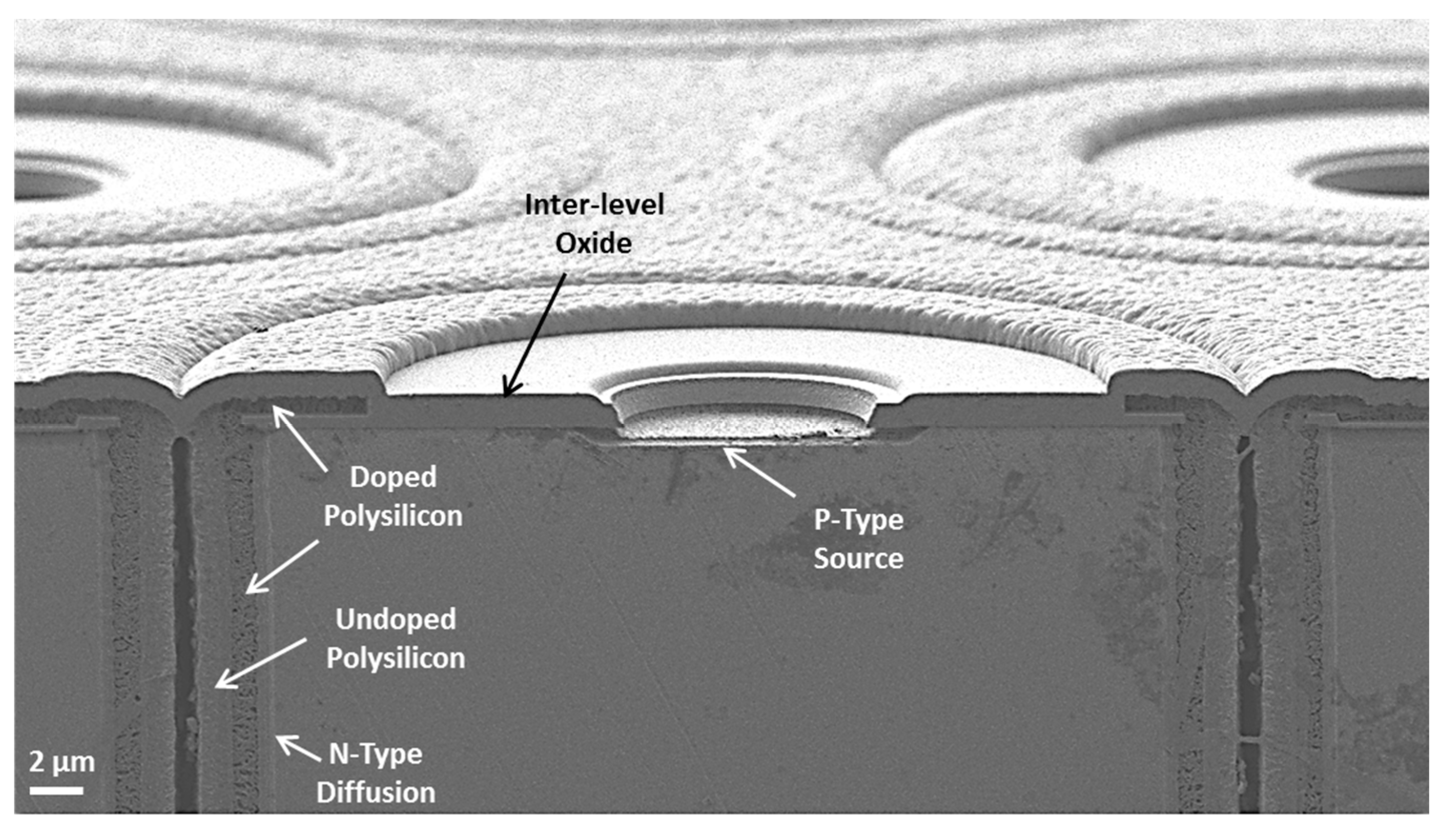
Figure 5 shows a SEM image of a V-JFET sample obtained just before the metal deposition. The tilted image allows distinguishing the arrangement of parallel cells, as well as the location of the peripheral gate runner and three of the floating guard rings. A layout scheme is also inset in the figure, for the shake of clarity. The cross section visible in the front confirms the good verticality of the etched trenches and their uniformity in depth.
The sample has been prepared with a reverse engineering technique to highlight the regions with higher doping concentration. In this sense, the amplified SEM image of
Figure 6, focused on the top side of an individual cell, shows the different elements present in the cell design. Highly doped regions, such as the doped polysilicon layer or the Source implant are clearly distinguishable. The n-type diffusion layer surrounding the trench edges can be also observed. From the image, it is clear that the second polysilicon layer is not thick enough to fill the entire trench hole. Even so, the combined effect of this layer with the thick inter-level oxide leads to a complete seal of the trench, thus allowing the process to continue with the following fabrication steps.
Due to the difficulty of obtaining highly resistive substrates with the good doping concentration precision, two different batches have been used for the fabrication of the first prototypes. The first one contains wafers with a nominal resistivity ranging between 500 and 1000 Ω·cm, which for p-type dopants is equivalent to NA = 1 to 3 × 10¹³ at/cm3; the second one presents a nominal resistivity between 150 and 500 Ω·cm, corresponding to NA ranging from 3 to 9 × 10¹³ at/cm3. The choice allows covering the whole range of optimum values discussed in the previous section, although the lack of accuracy in the actual NA value advise against the use of a single value for the other design parameters. Consequently, three different diameters (2r = 23, 29 and 35 µm) have been considered. Concerning the trench layout, values of D = 80 µm and W = 5 µm have been fixed. In addition, two cell-to-cell separation (S) values of 7 and 10 µm have been considered to test the structural stability of the arrangement if S is reduced.
4. Electrical Performance
The particular layout of the V-JFET transistor, with n-type Gate and p-type Source and Drain electrodes, forces the use of a specific measurement set-up. In order to avoid the forward bias of the channel-trench p-n junction, both the Gate-to-Source (VGS) and the Gate-to-Drain (VGD) voltages should be always greater than or equal to zero. A straightforward way to get this conditions is the application of a negative bias to the Drain and Source electrodes, while the Gate bias is always positive. This arrangement allows analyzing the forward conduction mode when 0 ≤ VGS < VOFF and VDS ≤ 0, whereas the forward blocking mode is obtained when VGS ≥ VOFF and VDS ≤ 0. The reverse mode can be also explored for VDS > 0, provided the VGD ≥ 0 restriction is always observed.
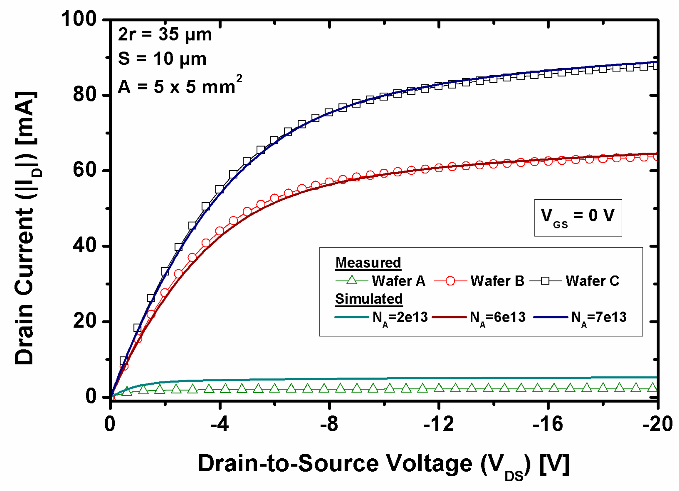
Taking this into account, the output (|
ID| vs.
VDS at
VGS = 0 V) and transfer (|
ID| vs.
VGS at
VDS >
VDS|SAT) characteristic curves have been measured in all the fabricated prototypes. For devices with equal design (i.e., with the same 2
r,
S and
A values), the measured current scales at different levels depending on the wafer of origin. By way of example,
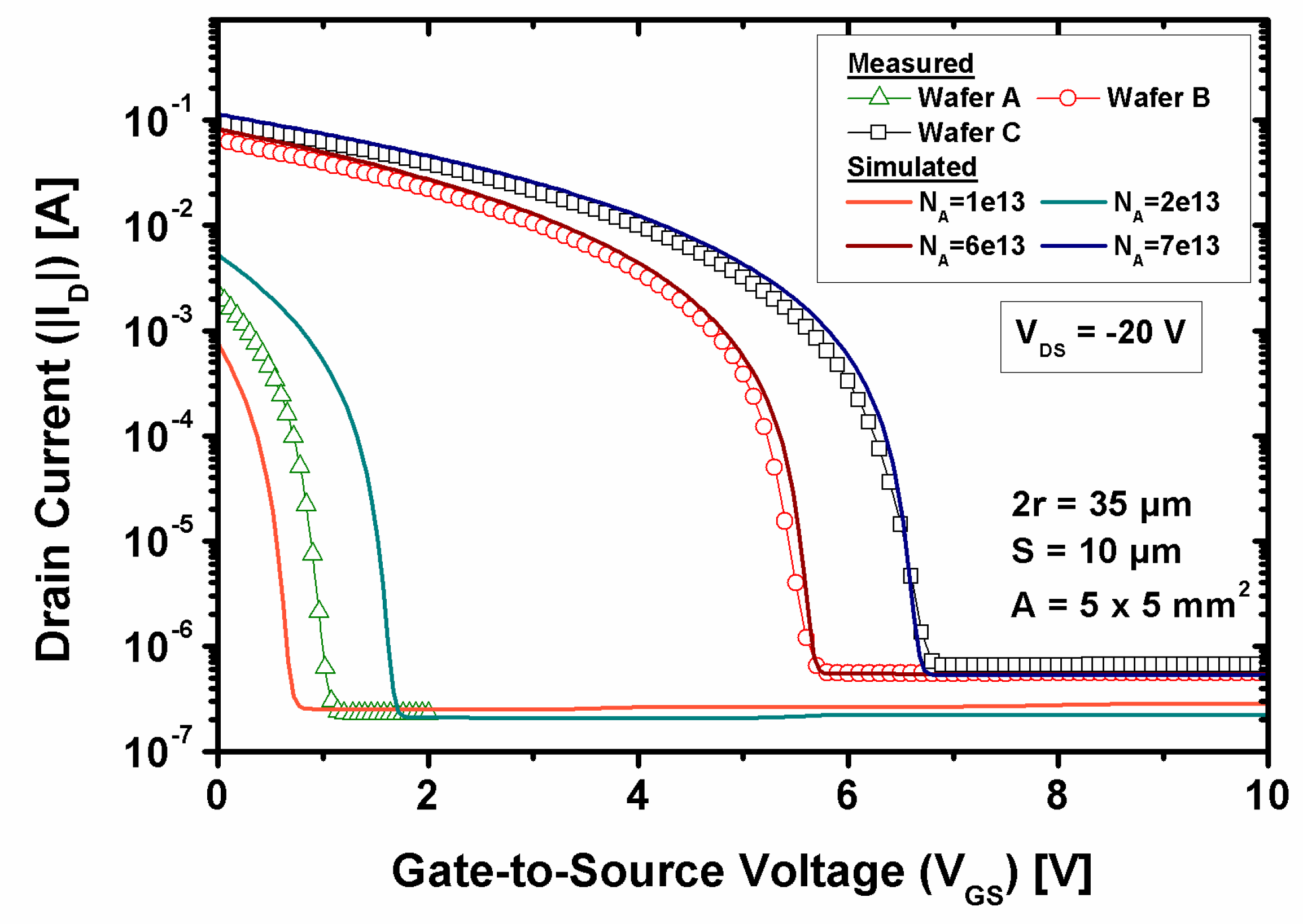
Figure 7 and
Figure 8 respectively shown the output and transfer characteristics for three representative 2
r = 35 µm samples fabricated on different wafers. The corresponding simulated curves for different
NA values are also included in the figures, and demonstrate great accordance with the observed performance. All the prototypes fabricated on the first batch of wafers, with nominal
NA between 1 and 3 × 10
13 at/cm
3, show characteristic curves as the ones labeled as Wafer A in the figures. For the prototypes of the second batch, where the nominal
NA ranges from 3 to 9 × 10
13 at/cm
3, two groups of curves (B and C) have been identified, with all the devices of a given wafer belonging to the same group. According to the simulations, wafers in the first batch yield in the lower part of the expected range of
NA values, since all the measured curves correspond to
NA between 1 and 2 × 10
13 at/cm
3. For their part, wafers used for the second batch had actual
NA values around 6 × 10
13 at/cm
3, for the group B, and 7 × 10
13 at/cm
3, for the group C, both in the higher side of the expected range. As a consequence, the intermediate values of the optimum range for
NA were not affordable in this study.
The average values of the main Figures of Merit (FoM) extracted from the measured characteristics are compiled in
Table 1. The values come from the measurement of 360 working VJFET devices. For devices fabricated on wafers of group A, low
ION and
VOFF values have been obtained, with only the 2
r = 35 µm designs achieving forward currents over the milliampere order and switching voltages close to 1 V. Besides, the low
NA value led to a relatively high on-state resistance (
RON) in the order of kΩ. For devices fabricated in the second batch (groups B and C),
ION ranges from more than 10 mA to almost 100 mA, mainly depending on the cell diameter. A significant reduction is observed in
RON, with values below 100 Ω for all the cases.
VOFF is strongly dependent on
r. Hence, prototypes with 2
r = 23 µm show
VOFF around 2 V, whereas the average
VOFF value approaches 4 V for the 29 µm case, and is always higher than 5 V if 2
r = 35 µm.
Concerning the forward blocking performance, the measured leakage current levels (
IOFF) are typically below the microampere order, with the majority of prototypes of group A showing
IOFF ~0.2 µA. The Gate leakage (
IG), both in conduction and blocking modes, averages current levels below 1 µA, with similar
IOFF values. However, a large
IG increase has been measured in some devices, particularly for high
VGS. Other devices show high leakage even at
VGS = 0 V. As it is considered a reliability issue, both cases have not been taken into account when extracting the average values listed in
Table 1.
The voltage capability of the fabricated prototypes has been also measured. The obtained VBD|FULL values show high variability and are too low, even considering that a large reduction with respect to the simulated VBD|CELL was expected. For prototypes of the group A, a maximum VBD|FULL = 675 V has been measured. Meanwhile, VBD|FULL is never higher than 300 V in the group B and group C devices. The breakdown point is located at the bottom of the peripheral trenches and the edge termination was optimized for a low substrate doping concentration (NA). The dependence of the edge termination efficiency on the substrate doping concentration is very strong and the drastic reduction of the voltage capability is directly related with high NA values of the available wafers. On the other hand, no correlation has been found between the voltage capability and the size of the cells, as prototypes with different r show similar VBD|FULL values. The variability in the measured VBD|FULL value and the influence of the implemented edge termination strategy are discussed in the next section.
Finally, it has to be noted that the dynamic performance has not been evaluated in this study, since the device is not conceived to work in switching mode.
5. Reliability
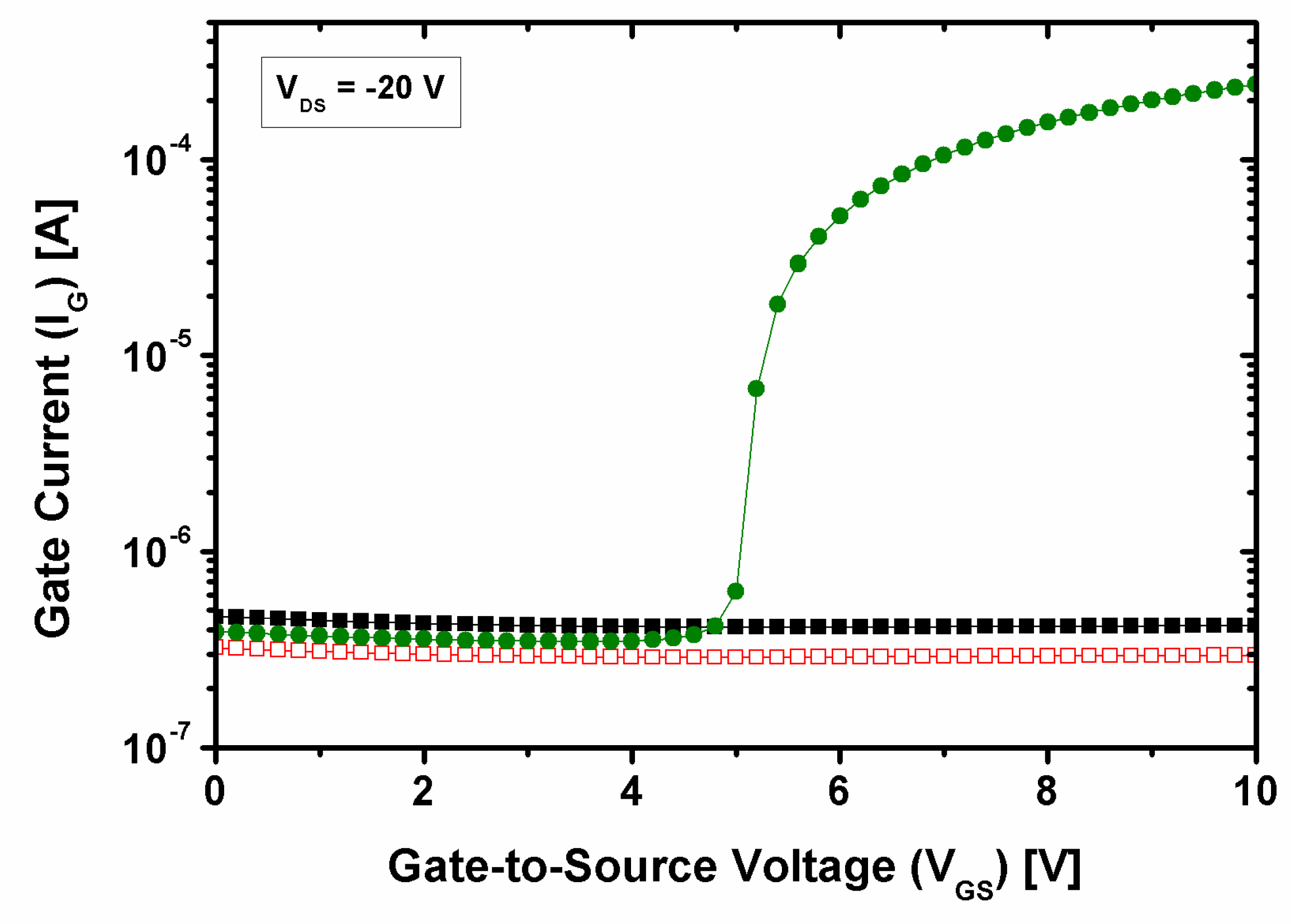
Two main reliability concerns have been found during the characterization of the V-JFET prototypes: an abnormal increase in the Gate leakage current in several devices working in forward blocking mode and a large variability of the voltage capability, even for devices with equal design, fabricated on the same wafer. In addition, the measured VBD|FULL values were always below the expectations. Both, issues have been specifically analyzed with the aid of lock-in infrared thermography technique.
Although most of the measured devices show Gate leakage in the order of a few hundreds of nanoamperes, approximately a 30% of the prototypes exhibit higher Gate currents, particularly when they are biased in the blocking mode.
Figure 9 shows the Gate current vs. Gate voltage characteristic for one of such malfunctioning devices, compared with the curves of two prototypes with standard performance. A sudden current increase takes place for
VGS >
VOFF, rising the Gate leakage to almost the milliampere order. Some other samples exhibit an analogous current increment, even with
VGS = 0 V. The Gate current drift is observed in devices for all the wafers, irrespective the particular design parameters. It cannot be attributed to a bulk effect, since measurements at low temperature (down to −30 °C) have not shown any scaling of the abnormal current level, whereas the standard Gate leakage was reduced according to the theoretical expectations. In addition, the Gate leakage increase leads to an immediate rise of the Source current, thus pointing to a short-circuit between the electrodes.
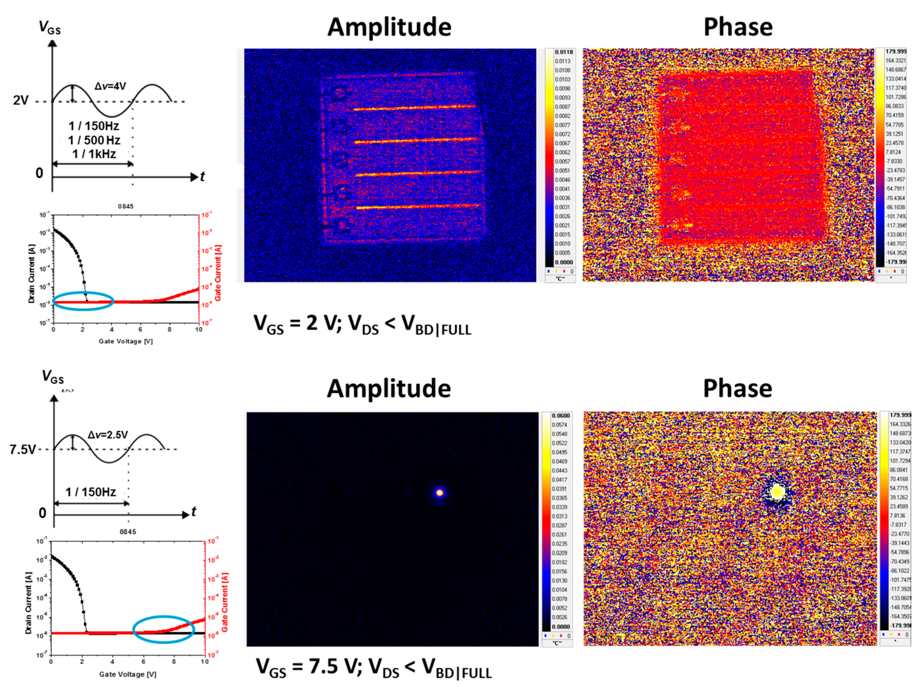
To analyze this case, a lock-in infrared measurement [
20] was performed on a malfunctioning device by modulating the Gate voltage with a sine-like voltage of certain amplitude (ΔV), around a specific
VGS value [
21,
22].
VDS is held constant well below the
VBD|FULL value. For
VGS < 2 V, the transistor is biased in the conduction mode and low Gate leakage is observed. An infrared thermography image was composed, by obtaining 15,000 frames while the transistor Gate was being modulated with Δ
V = 4 V and lock-in frequency,
flock-in = 500 Hz. As shown on the top side of
Figure 10, uniform dissipation takes place throughout the whole device, and no leakages are observed. Conversely, when the Gate is modulated in the same way around
VGS = 7.5 V, a conspicuous hot-spot is clearly observed. The infrared thermography, represented in the bottom side of
Figure 10, shows how the Gate leakage increment is completely driven through the hot-spot, with all the heat generation focused on a single location. Although the issue is still under study, a pin-hole in the inter-metal oxide has been identified as the most probable cause of the hot-spot generation, requiring a future improvement of its quality for better yield.
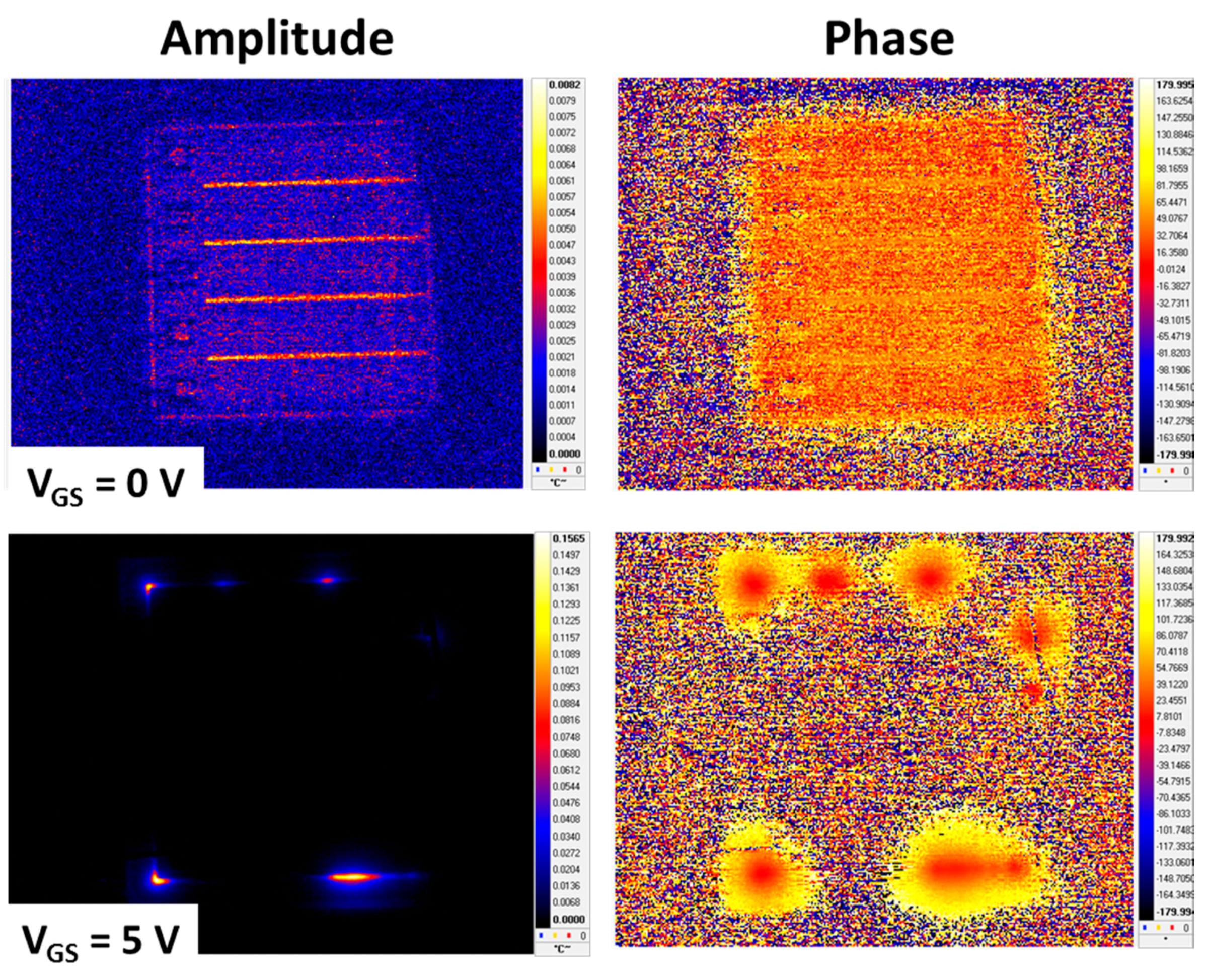
The low breakdown voltage of the samples was also studied with the aid of the infrared thermography analysis. In this case, Drain voltage modulation was performed, while
VGS is held constant at different values to explore both the forward conduction and forward blocking operational modes of the transistor. For
VDS <
VBD|FULL, no signal was discerned, irrespective the
VGS considered, since the devices are not dissipating enough power. When the transistor is biased close to the breakdown (
VDS = − 300 V), a higher signal level can be obtained, as a consequence of the increase in power dissipation, as shown in images from
Figure 11. For
VGS = 0 (top side of the figure), with the transistor working in forward conduction, uniform dissipation is perceived. When the transistor is switched-off into the blocking mode, the dissipation focuses at the periphery. As shown in the bottom side of
Figure 11, for
VGS = −10 V, several hot spots appear on the peripheral Gate runner. Two main conclusions can be extracted from the analysis: The Gate-to-Drain breakdown is located at the peripheral Gate runner, thus indicating that the floating guard rings are not contributing to increase the voltage capability of the device; this can be identified as the main cause of the low
VBD|FULL value measured in all the devices. Besides, the power dissipation is not uniformly distributed all around the periphery; on the contrary, several hot-spots of different size can be distinguished. The presence of these weak points in the design may be the origin of the high variability in
VBD|FULL observed among different devices. The edge termination strategy is now being revisited to achieve a more robust and uniform breakdown behavior.
6. Radiation Hardness
Two different mechanisms are responsible for the radiation effects on the electronic devices [
23]: ionizing radiation introduces ionization damage (ID), whereas non-ionizing radiation induces displacement damage (DD). In both cases, the consequences on the device performance are generally the result of the accumulative effect of the introduced damage. In addition, single event effects (SEE) may occur when a highly energetic particle introduces large amount of damage (usually ID) within a particularly sensitive region of the electronic device [
24]. ID is especially harmful for dielectric materials, where the introduced damage leads to the accumulation of trapped charge. This charge, which can eventually become permanently fixed, is able to modify the distribution of the electrostatic potential in the device. In this sense, MOS transistors and other insulated Gate devices are specifically sensitive to ID [
25]. On the contrary, DD affects the semiconductor layers into a greater extent, as the semiconductor lattice is affected by the introduction of active defects and dislocations. Bipolar transistors and other devices with large depleted regions, such as the semiconductor radiation detectors, have been reported especially sensitive to displacement damage [
26].
High radiation tolerance is expected in the V-JFET thanks to its specific design. The absence of a Gate oxide and other insulator layers within the active regions of the device makes the V-JFET less sensitive to the accumulated effects of the ionizing radiation. Although a certain increase can be expected in the leakage current, the use of a p-type substrate (less sensitive to DD [
27]) and the volume conduction through relatively wide channels also prospected radiation hardness as far as the non-ionizing radiation is concern. SEE are not considered a probable cause of fail, thanks to the large number of parallel cells present in the transistor layout: even if an individual cell becomes affected by a SEE, the possible current increase represents a minor alteration in the overall current of the whole arrangement. In this sense, SEE were not tested in this work.
To analyze the effect of ID, 30 V-JFET samples were exposed to different doses of a pure gamma radiation source. Gamma radiation consists of high energetic photons able to produce large amount of ID, although a minor amount of DD can be also introduced into the semiconductor layers, from the secondary electrons released by Compton Effect. Irradiations, up to a total ionizing dose (TID) of 100 Mrad(Si), corresponding to a dose rate of 389 krad(Si)/h, where performed at the NAYADE
60Co water well source of the CIEMAT [
28], in Madrid (Spain). Details of the experimental set up and a thorough analysis of the obtained results can be found in [
29]. The performance of the irradiated devices was almost the same as before the irradiation. Most of the FoM (e.g.,
VOFF,
IOFF,
IG, or
VBD|FULL) remained unaffected even for the highest TID considered. The single relevant effect was a minor reduction of the conduction current in the forward mode, which led to lower I
ON, and higher R
ON values. Nevertheless, the FoM modification achieved a maximum of ~20% for 50 Mrad(Si) and saturates for higher TID, whereas was almost negligible below 10 Mrad(Si) [
29]. All this considered, the V-JFET prototypes have been proved to remain fully operative after a high dose pure ionizing irradiation.
The effects of DD are normally studied in samples irradiated with hadrons, e.g., neutrons, protons or pions. Among them, neutrons are preferred, since the absence of electrical charge leads to almost pure DD effects into the semiconductor devices. Hence, 55 V-JFET samples were irradiated at different neutron fluences in a TRIGA-type nuclear reactor at the Jožef Stefan Institute in Ljubljana (Slovenia) [
30]. The particular nature of the irradiation source produces neutrons with a continuous spectrum of energies (including thermal neutrons), which are then normalized according to the NIEL scaling [
31], and expressed by means of a 1-MeV neutron equivalent fluence (n
eq) magnitude, which takes into account the weighted effect of all the non-ionizing contributions.
After high neutron irradiation fluence up to of 2 × 10
13 n
eq/cm
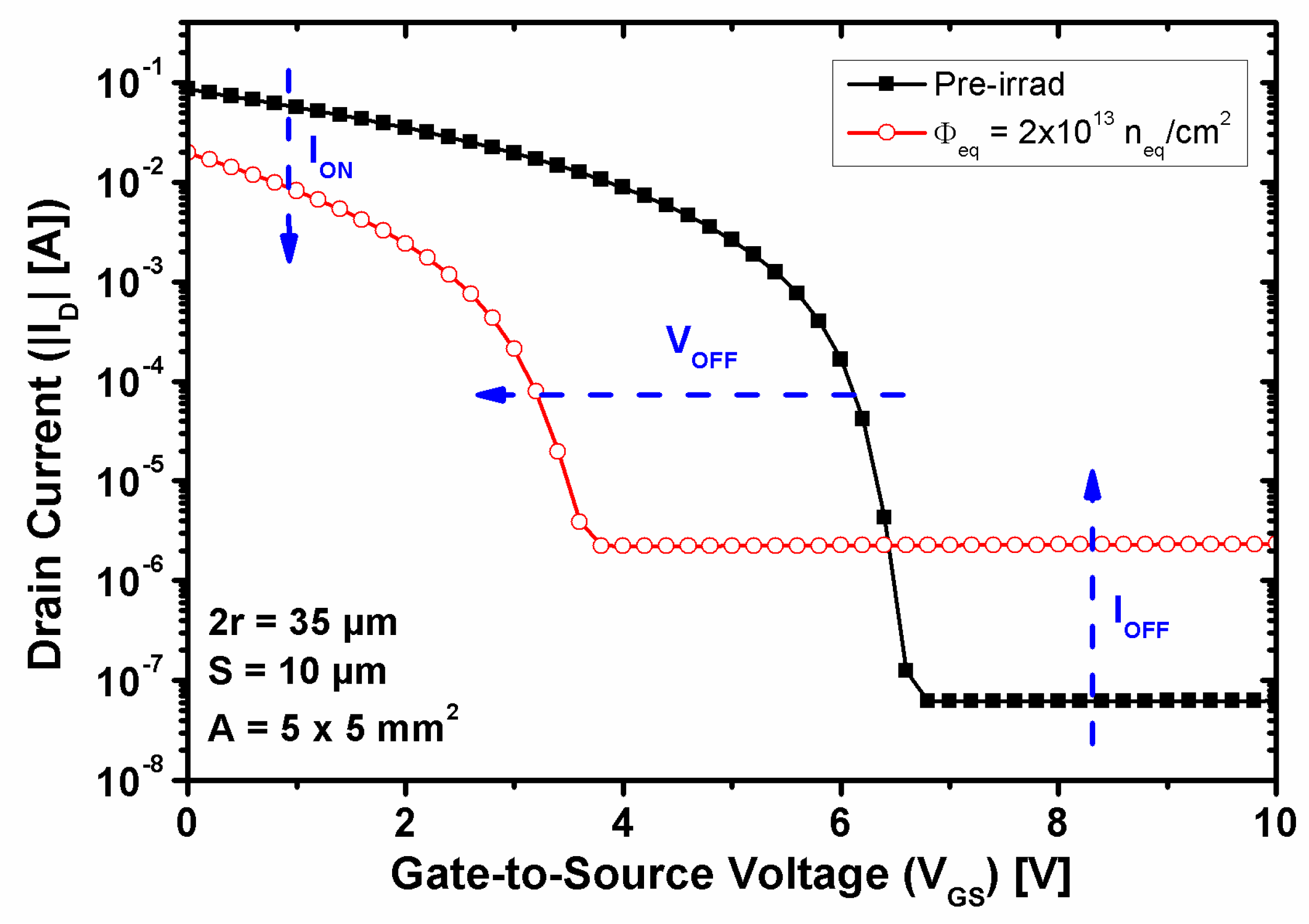
2, the V-JFET samples still remained fully operative, although the DD effects were not negligible. The variation in the transistor performance can be observed in
Figure 12, where the transfer characteristic of an irradiated sample is compared with the curve measured before the irradiation. The sample was fabricated on a p-type substrate with a doping concentration of 7 × 10
13 cm
−3. The forward current exhibits a reduction in the range of 60 ma, depending on the sample and on the specific layout, whereas the blocking leakage current increases notably, from 0.1 to 2 µA. Similar increment is observed in the Gate leakage current. Besides,
VOFF experiences a reduction of almost 3 V.
The increase in the blocking and Gate leakage currents were expected, since it is typically observed in radiation detectors fabricated on p-type silicon substrates [
32]. This effect is generally associated with the introduction of a large amount of DD defects, which can act as generation-recombination centers in the depleted regions of the affected silicon. In contrast, the observed effects in the undepleted silicon (i.e., the
VOFF and the forward current reductions) can be associated with a decrease in the effective doping concentration of the substrate. Although this effect is still under study, it can be due to an acceptor removal process, already reported in the literature [
33], and analogous to the well documented donor removal effect, associated to DD effects on n-type silicon substrates [
24].
7. Conclusions
A new Vertical JFET technology has been developed at Centro Nacional de Microelectrónica (IMB-CNM, CSIC) in Barcelona, for harsh radiation applications. Fabricated on a p-type silicon substrate, the new V-JFET transistor consists of a large arrange of parallel cells (typically 10,000), each one of then surrounded by a trench of ring shape, deeply etched in the silicon substrate. The trench acts as the Gate electrode thus allowing vertical conduction through the confined silicon channel as well as a low switch-off voltage. The actual characteristics of the whole device are strongly related with the values of several design and technological parameters (i.e., the cell radius, the trench depth, the substrate doping concentration, and the total area of the device). A thorough optimization of the final design according to the values of these parameters has been discussed in this paper. The technological process was also outlined, with a particular emphasis laid on the trench etching and filling steps, which are crucial for attaining working prototypes.
After the fabrication, the V-JFET samples were fully characterized and the main results have been compiled here. The measured performance is in very good agreement with the simulation predictions, with forward current levels up to the 100 mA level, switch-off voltage ranging between 1 and 6 volts, depending on the cell radius and the substrate doping concentration, and blocking current and Gate leakage typically below the microampere order. Two main reliably issues have been held in the article, too: the relatively low voltage capability of the fabricated prototypes, and the rising of the blocking current in several devices. Both cases have been investigated with the aid of the lock-in infrared thermography technique, and the results point to an ineffective design of the edge termination region, in the first case, and to the presence of pin-holes in the inter-metal oxide. Still under study, both issues will be carefully addressed in the next batch production.
The radiation hardness of the V-JFET has been also tested with gamma and neutron irradiations up to total ionizing dose of 100 Mrad(Si) and equivalent fluence of 2 × 10¹³ neq/cm2, respectively. Minor effects have been found as far as the gamma ionizing damage is concern. For its part, the displacement damage introduced by neutrons is able to notably modify the characteristic curves of the irradiated devices. Nevertheless, the evaluated samples remain fully operative under the radiation levels considered in this study.


 ,
, 


