
Isolated DC-DC Converter for Bidirectional Power Flow Controlling with Soft-Switching Feature and High Step-Up/Down Voltage Conversion

Abstract
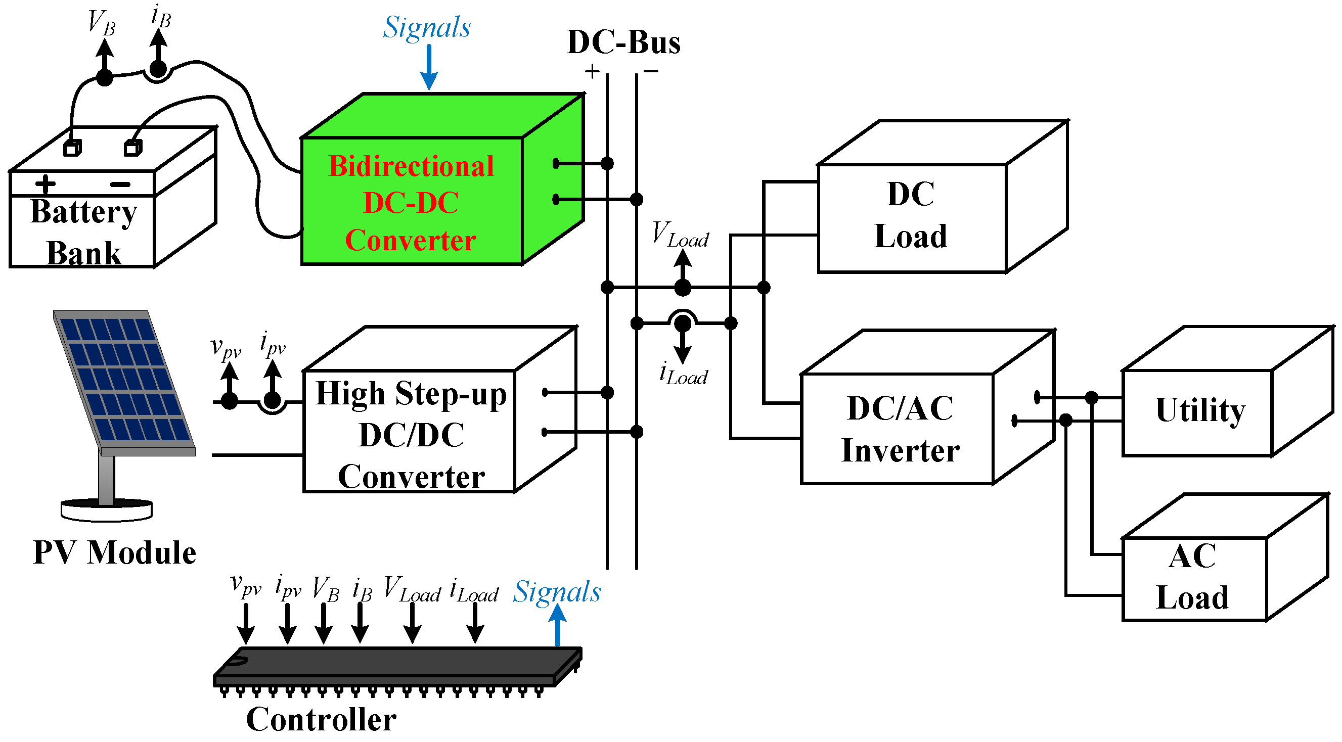
:1. Introduction
- (1)
- No matter in buck or boost mode, the energy stored in leakage inductors, Lk1 and Lk2, can be recycled without any snubber mechanism or clamped circuit.
- (2)
- All active semiconductor components can be switched with ZVS or zero current switching (ZCS) to eliminate switching losses.
- (3)
- Switches S1–S4 endure a low voltage stress so that semiconductor device with a smaller Rds(on) can be chosen to reduce conduction losses.
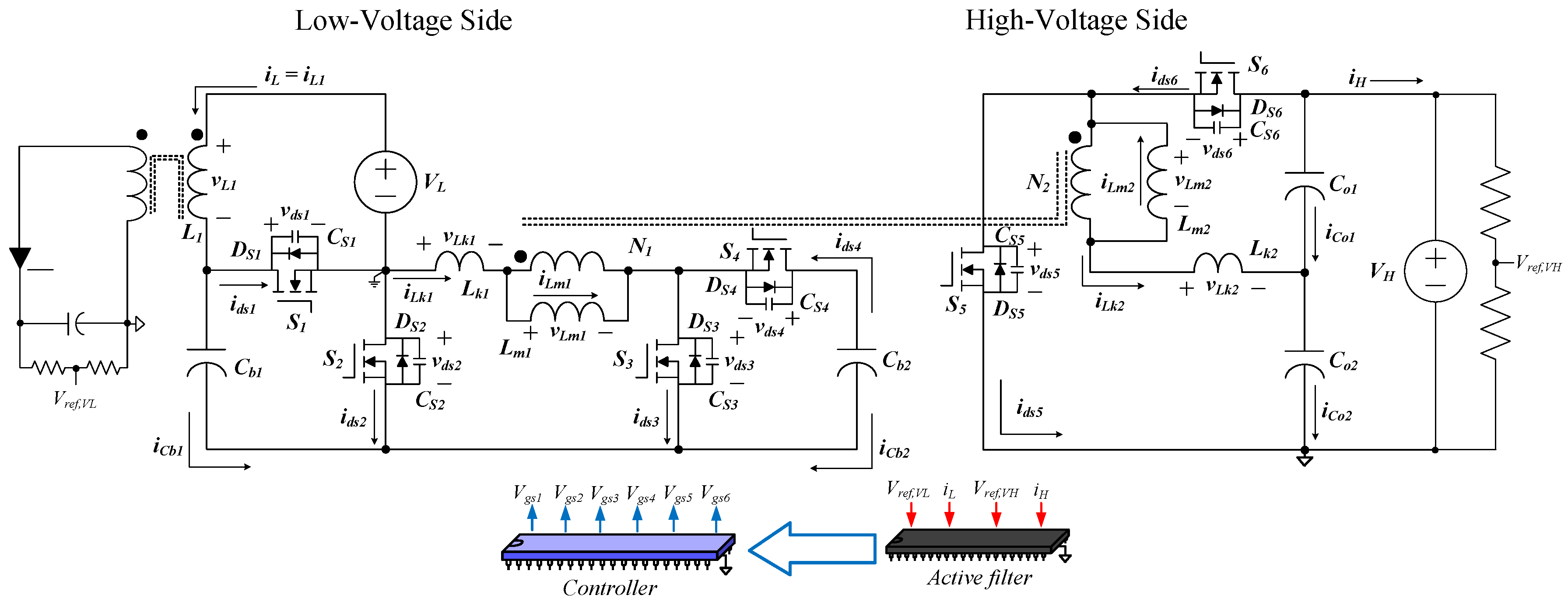
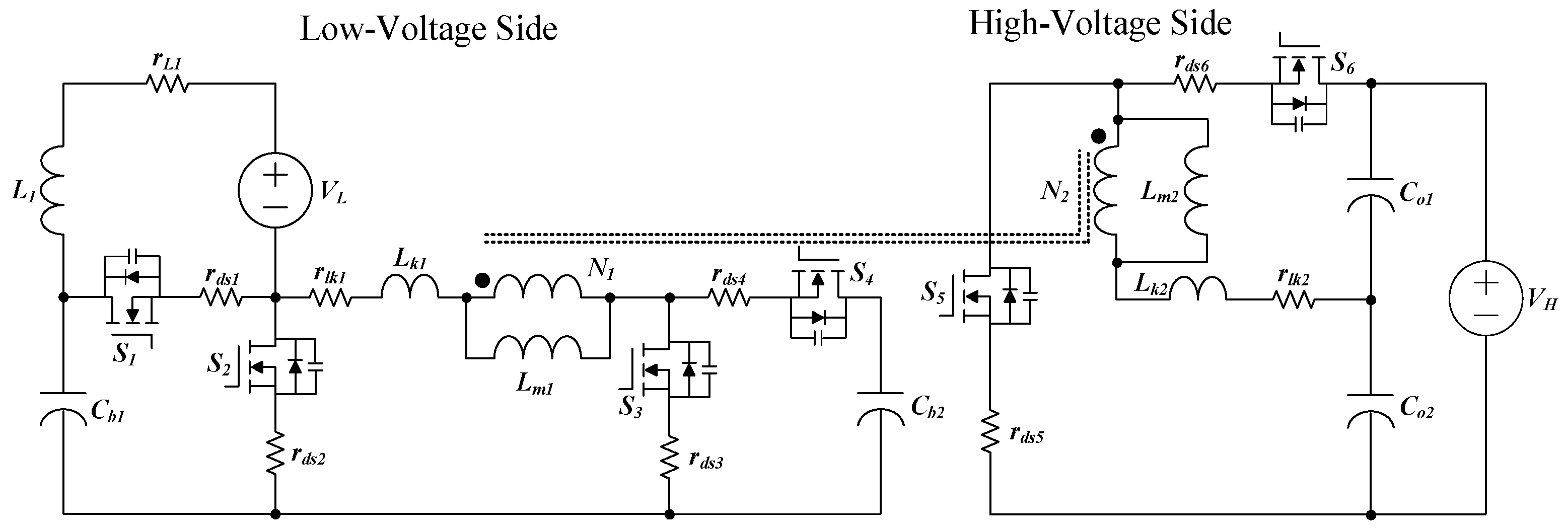
2. Operation Principle of the Proposed Converter
- (1)
- In Figure 2, capacitances of Cb1, Cb2, Co1, and Co2 are large enough so that all the voltages across them can be regarded as constant in a switching cycle.
- (2)
- Parasitic capacitor and body diode of each switch are considered, but the internal resistance is neglected.
- (3)
- The leakage inductance of the coupled inductor is much less than magnetizing inductance.
- (4)
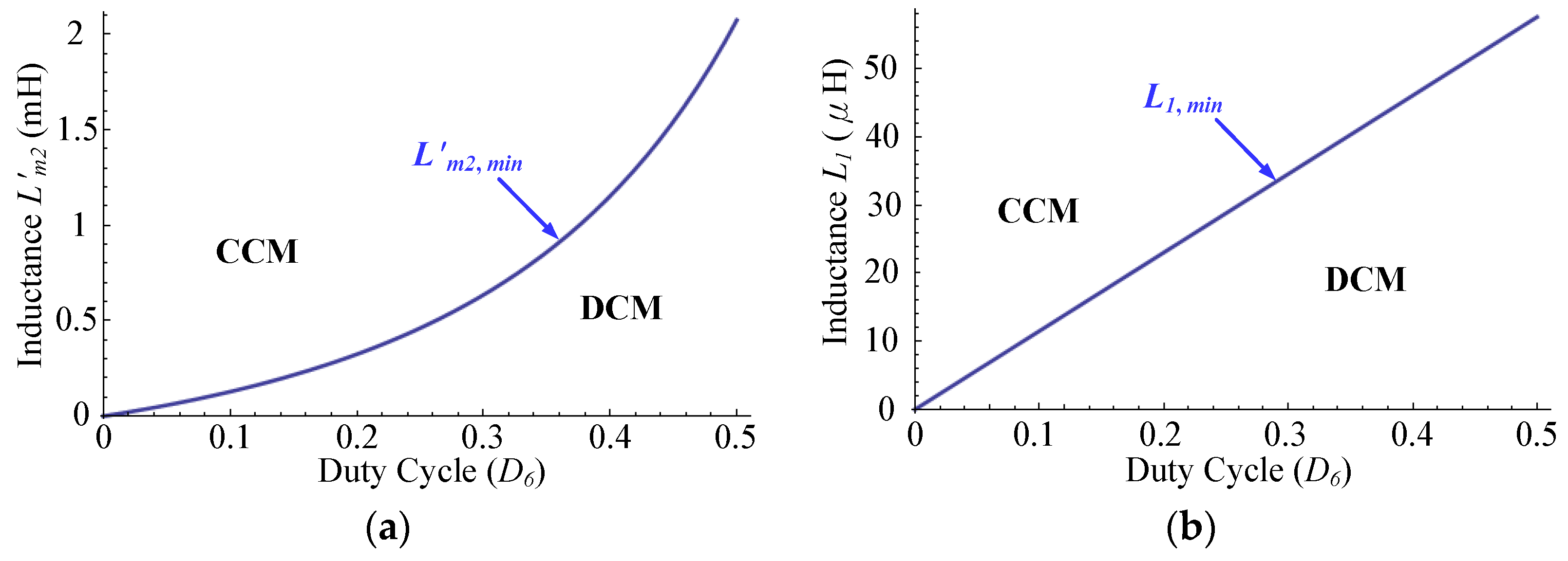
- All the magnetic components are designed in continuous conduction mode (CCM).
- (5)
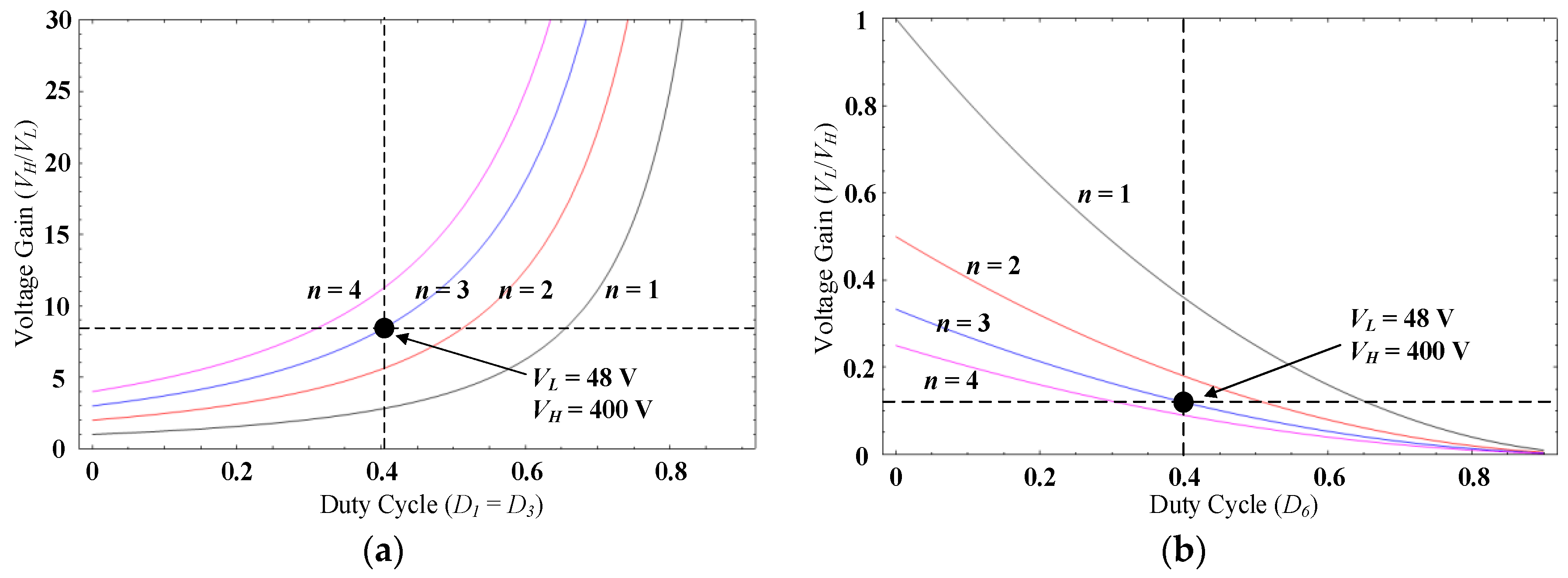
- The turns ratio of secondary to primary of the coupled inductor, N2/N1, is defined as n.
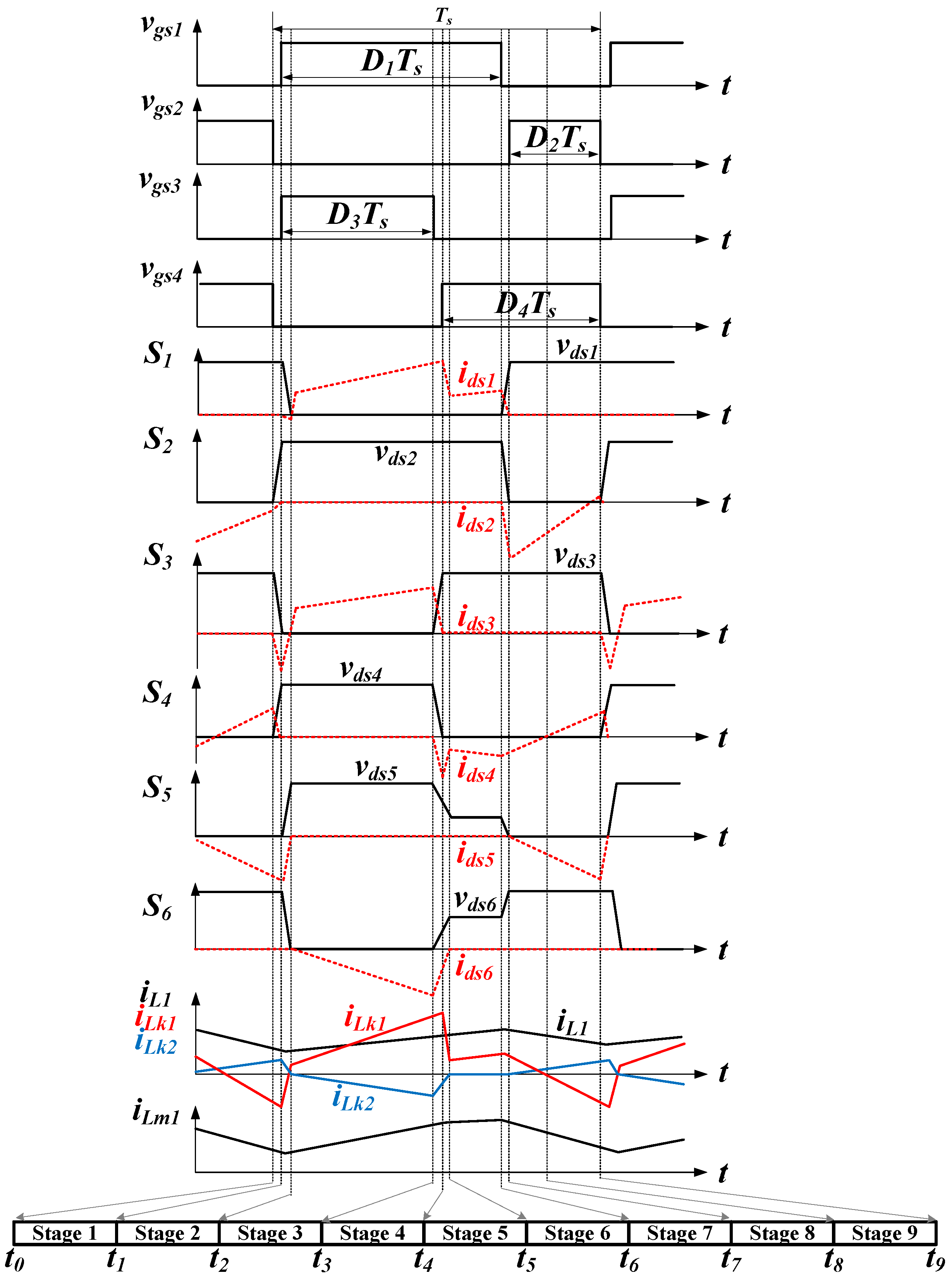
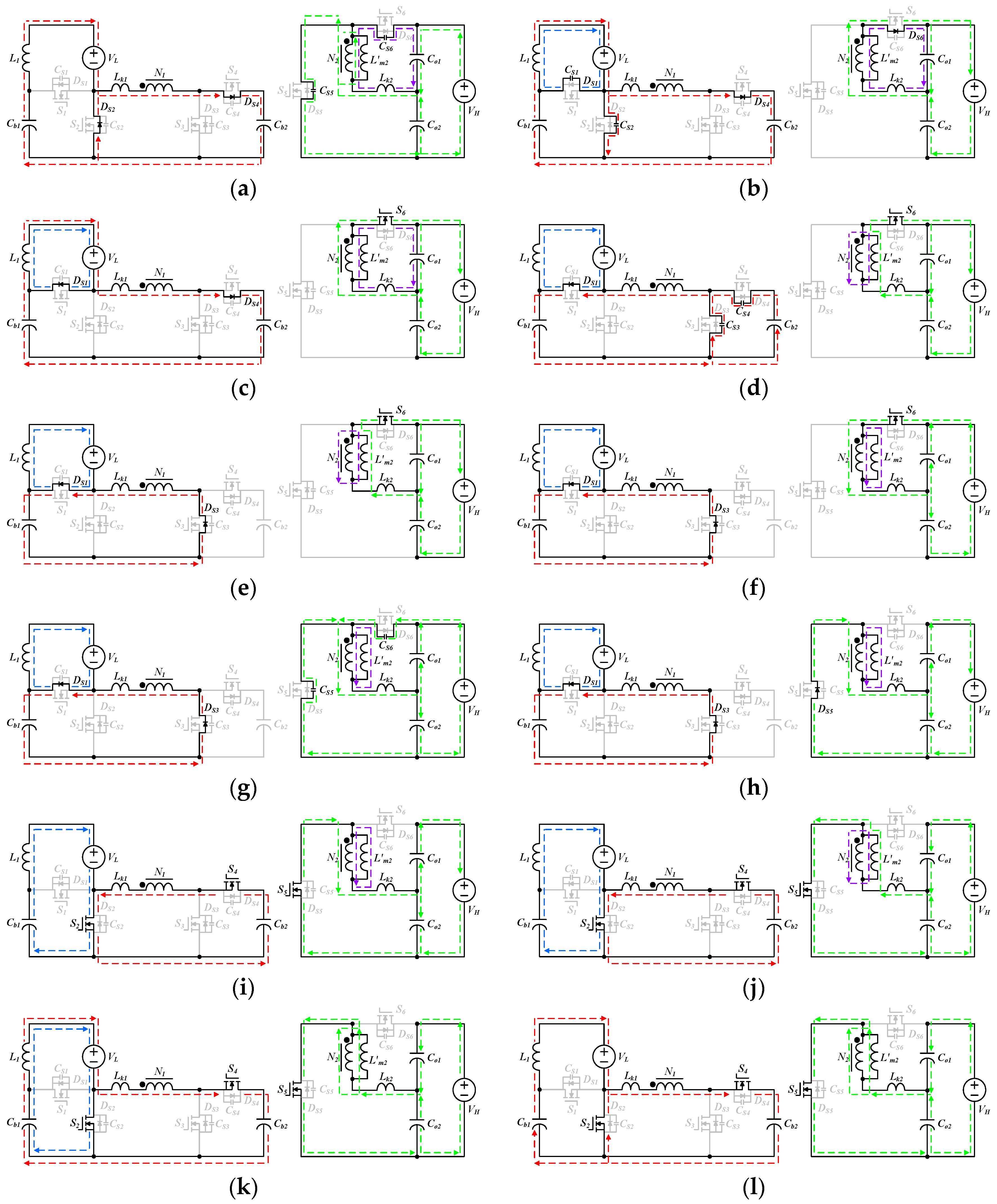
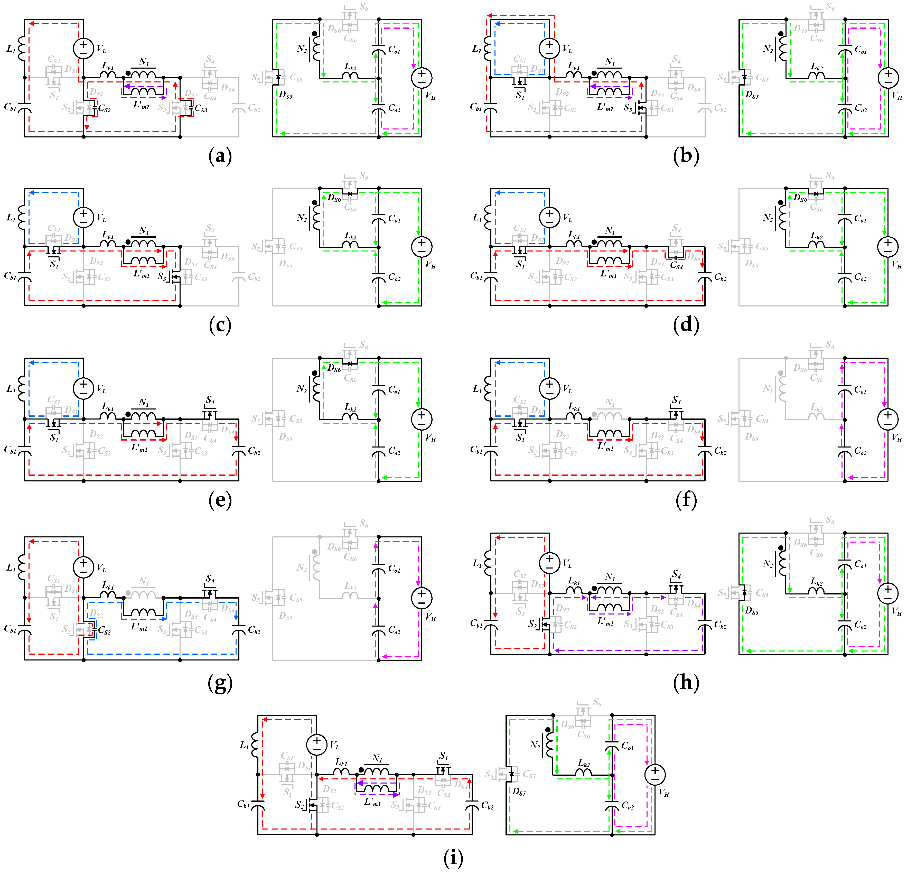
2.1. Step-Up Mode
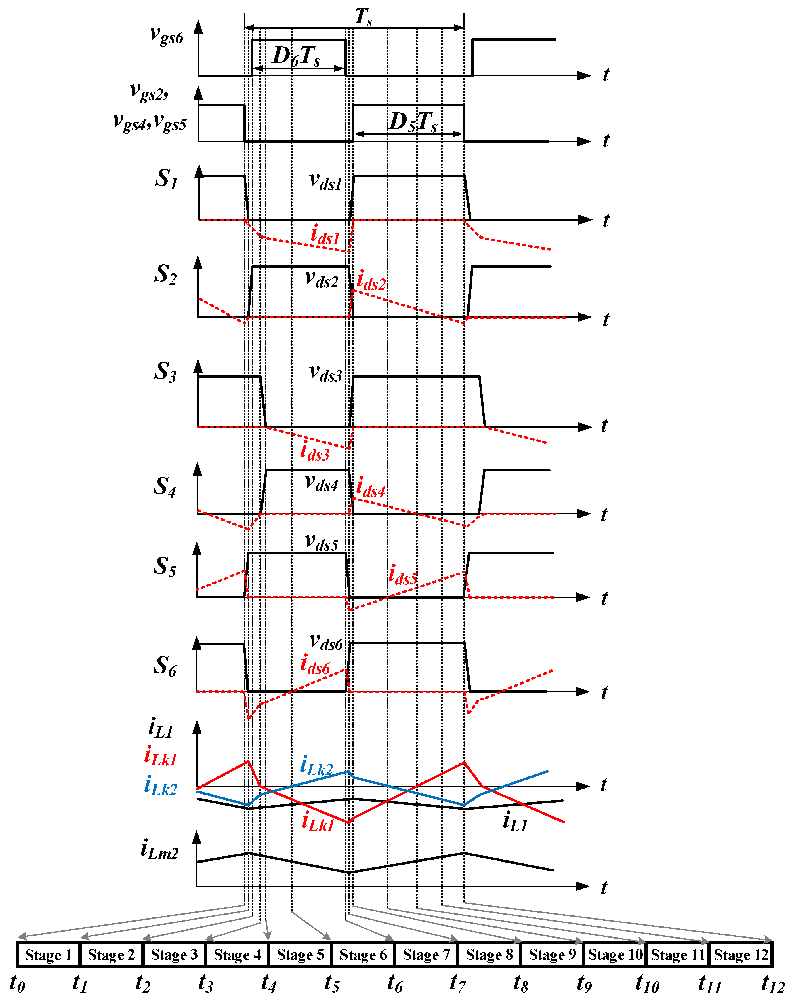
2.2. Step-Down Mode
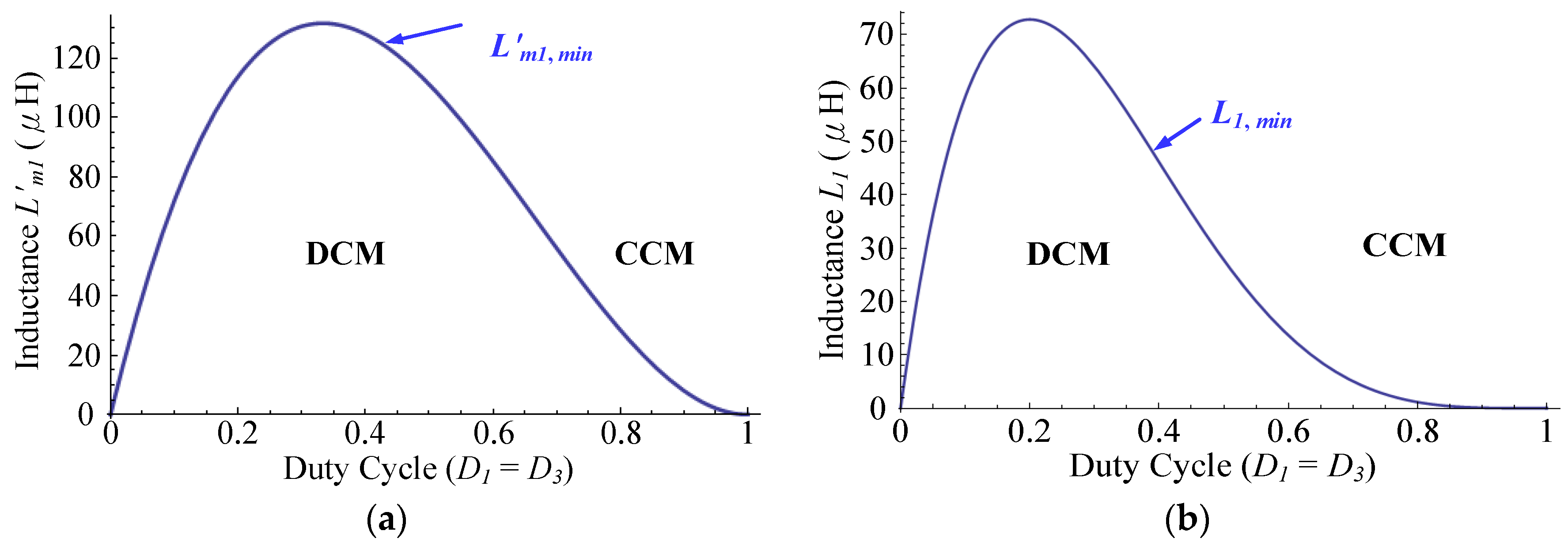
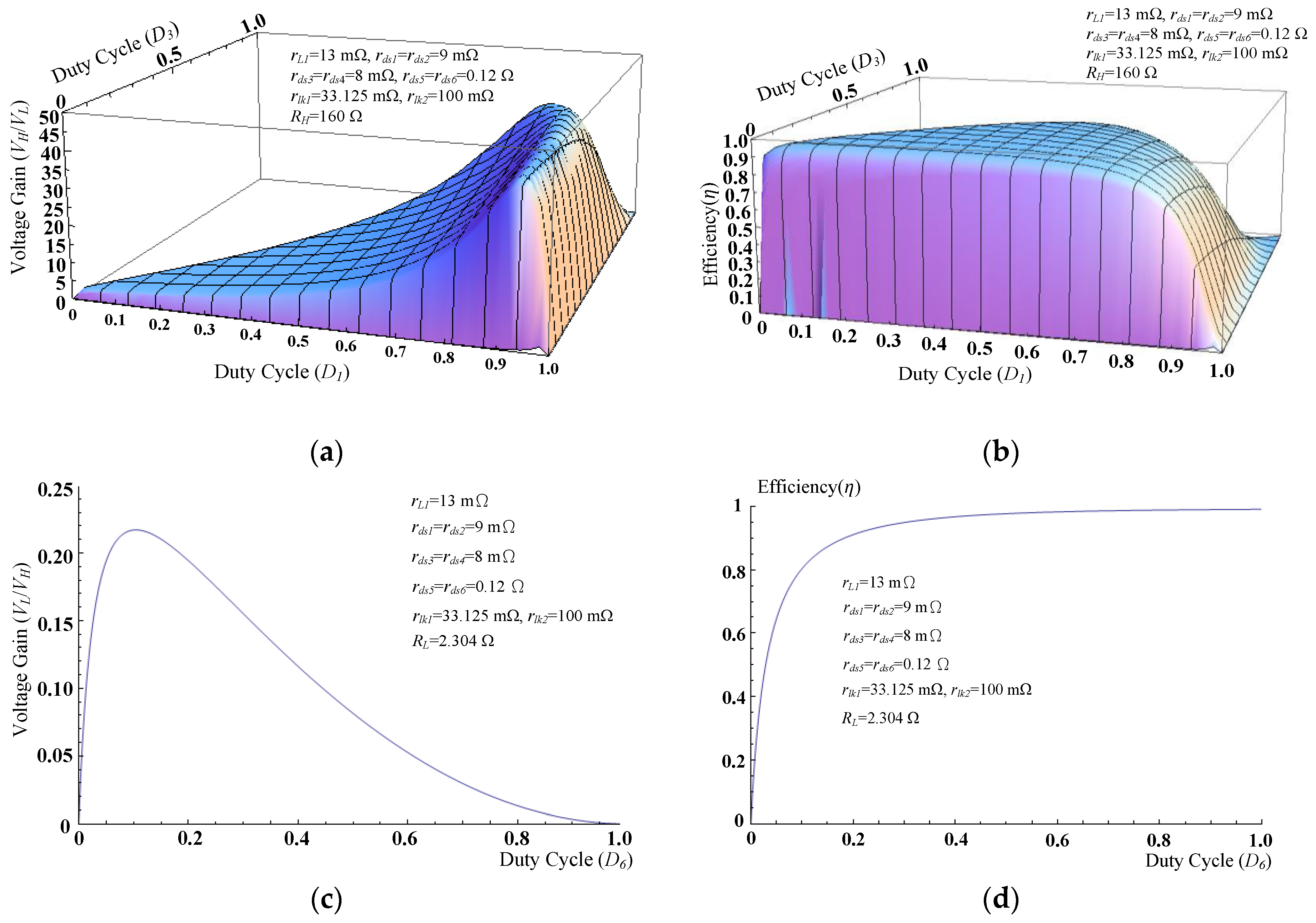
3. Steady-State Analysis
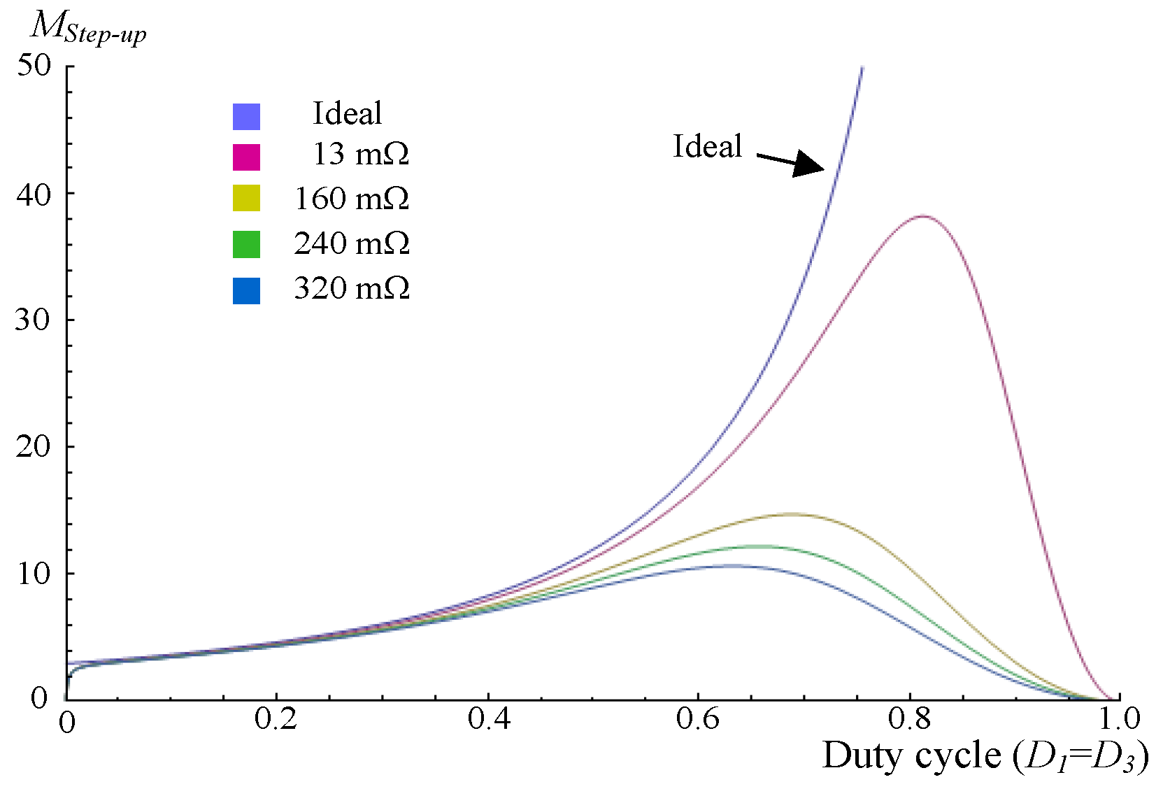
3.1. Step-Up Mode
3.2. Step-Down Mode
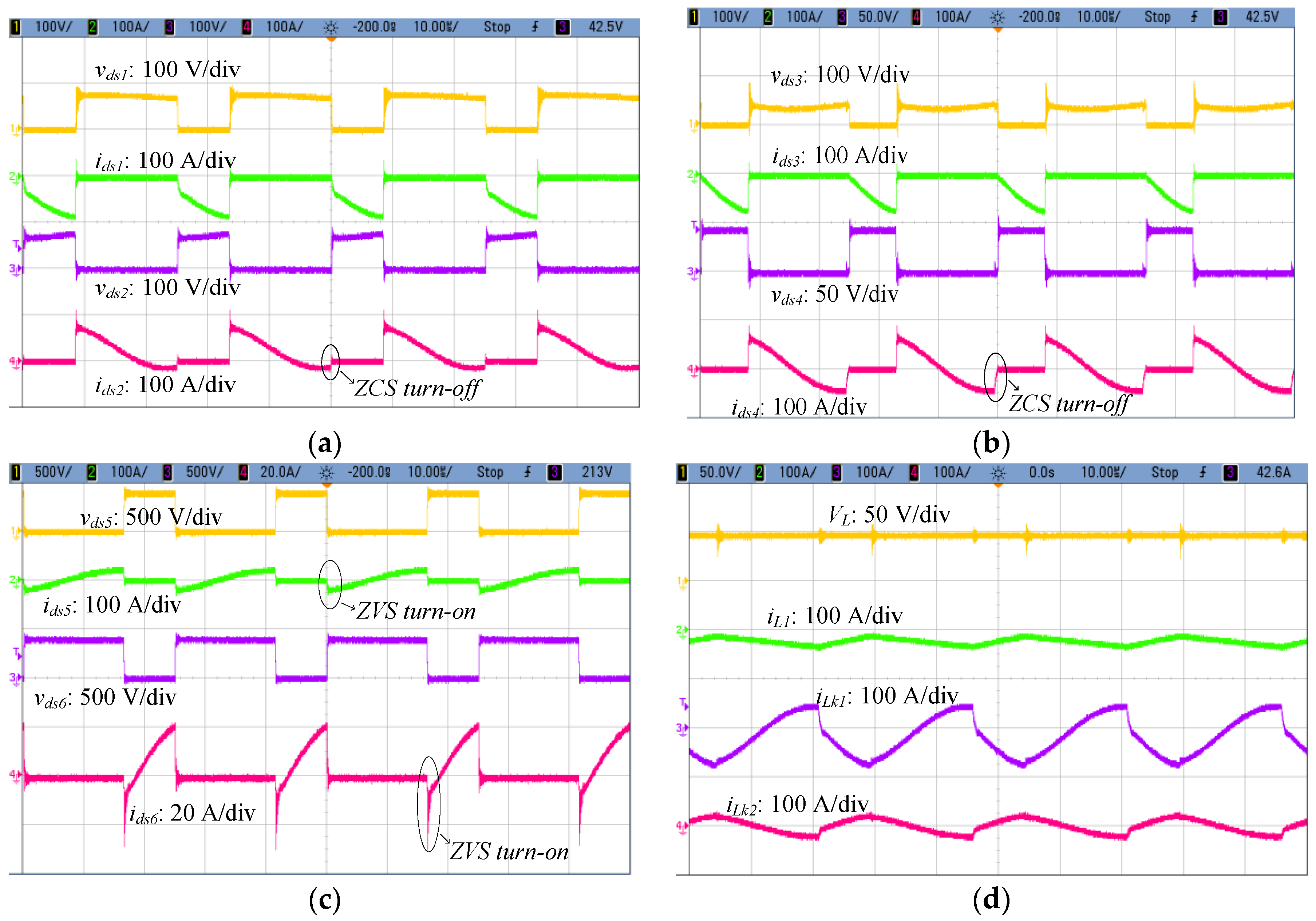
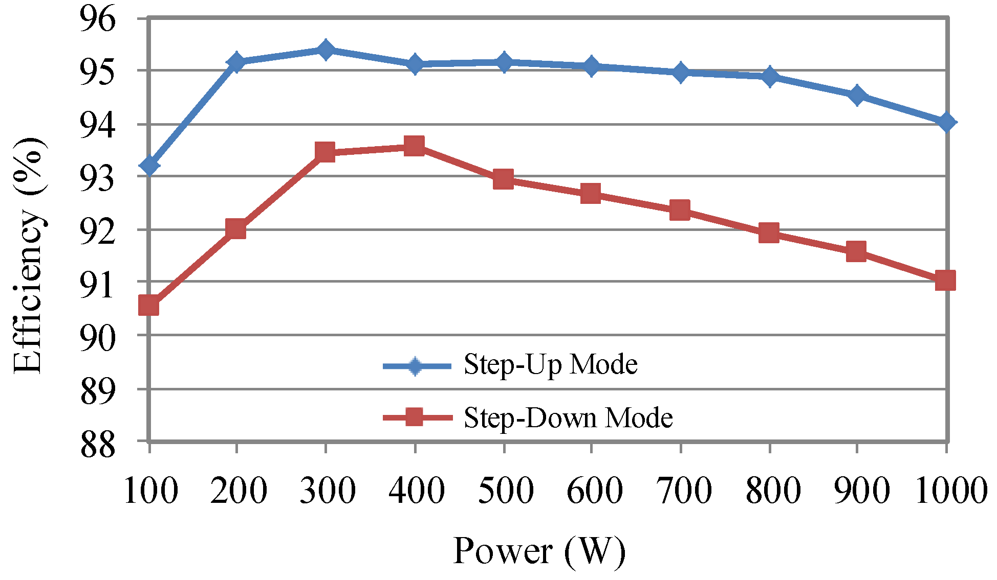
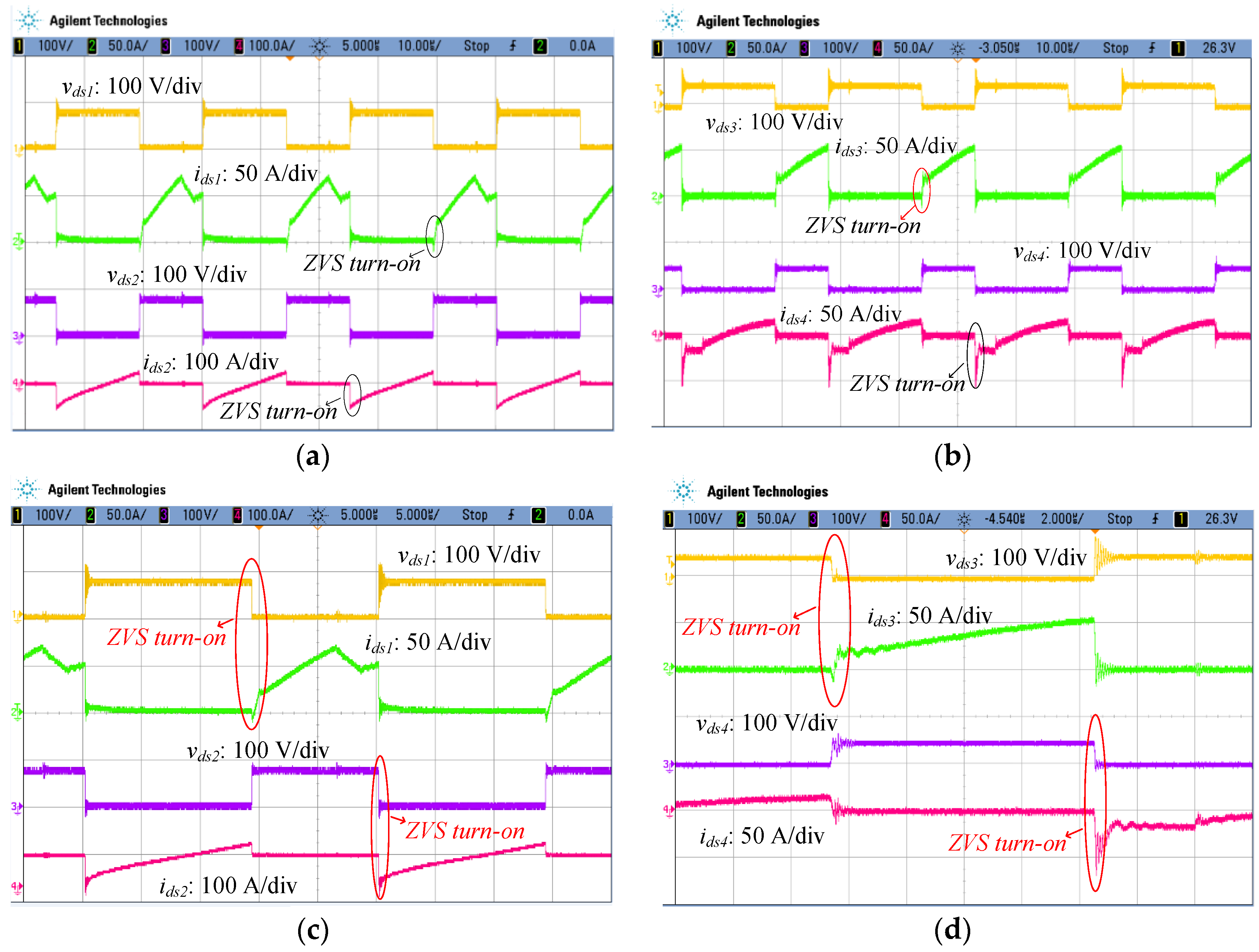
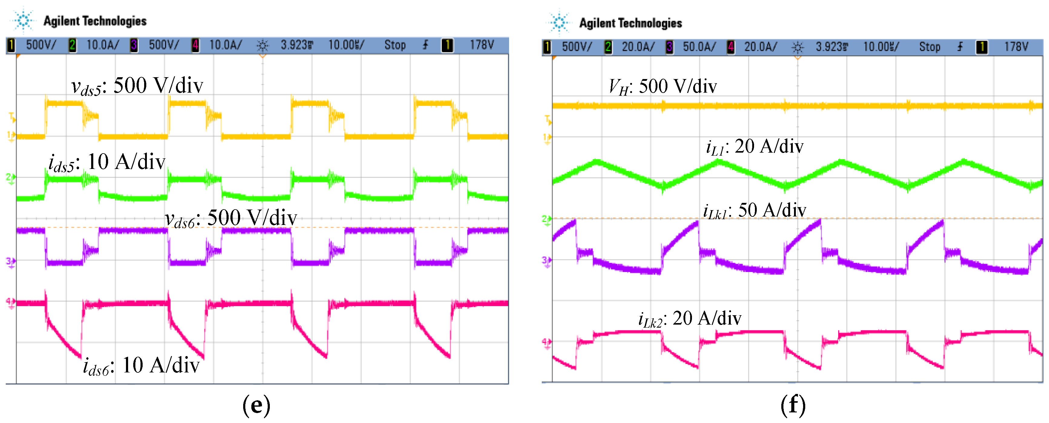
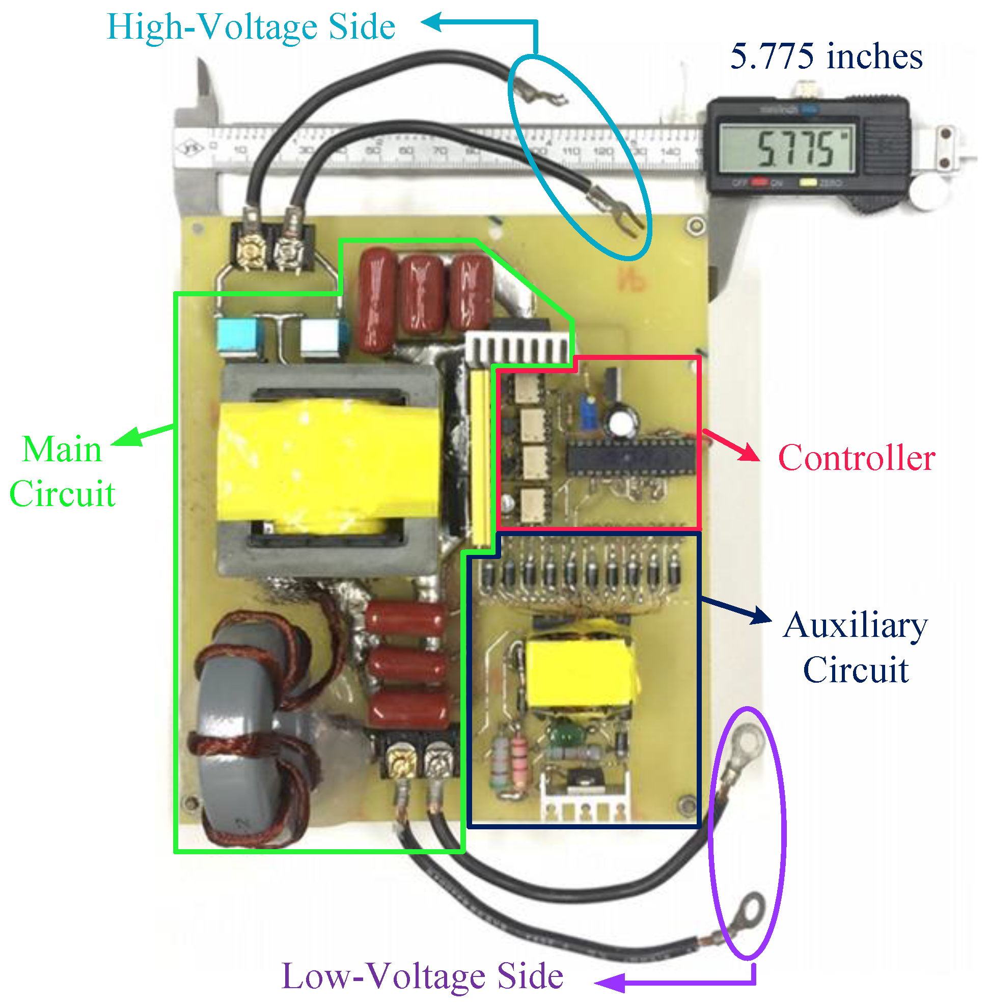
4. Experimental Results
5. Conclusions
Acknowledgments
Author Contributions
Conflicts of Interest
References
- Shen, C.-L.; Chiu, P.-C.; Lee, Y.-C. Novel Interleaved Converter with Extra-High Voltage Gain to Process Low-Voltage Renewable-Energy Generation. Energies 2016, 9, 871. [Google Scholar] [CrossRef]
- Pinto, R.; Mariano, S.; Calado, M.R.; de Souza, J.F. Impact of Rural Grid-Connected Photovoltaic Generation Systems on Power Quality. Energies 2016, 9, 739. [Google Scholar] [CrossRef]
- Elsaharty, M.A.; Ashour, H.A.; Rakhshani, E.; Pouresmaeil, E.; Catalão, J.P.S. A Novel DC-Bus Sensor-less MPPT Technique for Single-Stage PV Grid-Connected Inverters. Energies 2016, 9, 248. [Google Scholar] [CrossRef]
- Lai, C.-M. Development of a Novel Bidirectional DC/DC Converter Topology with High Voltage Conversion Ratio for Electric Vehicles and DC-Microgrids. Energies 2016, 9, 410. [Google Scholar] [CrossRef]
- Xue, L.-K.; Wang, P.; Wang, Y.-F.; Bei, T.-Z.; Yan, H.-Y. A Four-Phase High Voltage Conversion Ratio Bidirectional DC-DC Converter for Battery Applications. Energies 2015, 8, 6399–6426. [Google Scholar] [CrossRef]
- Liu, K.-B.; Liu, C.-Y.; Liu, Y.-H.; Chien, Y.-C.; Wang, B.-S.; Wong, Y.-S. Analysis and Controller Design of a Universal Bidirectional DC-DC Converter. Energies 2016, 9, 501. [Google Scholar] [CrossRef]
- Jiang, J.; Bao, Y.; Wang, L.Y. Topology of a Bidirectional Converter for Energy Interaction between Electric Vehicles and the Grid. Energies 2014, 7, 4858–4894. [Google Scholar] [CrossRef]
- Shi, X.; Jiang, J.; Guo, X. An Efficiency-Optimized Isolated Bidirectional DC-DC Converter with Extended Power Range for Energy Storage Systems in Microgrids. Energies 2013, 6, 27–44. [Google Scholar] [CrossRef]
- Ahmadi, M.; Mohammadi, M.-R.; Adib, E.; Farzanehfard, H. Family of non-isolated zero current transition bi-directional converters with one auxiliary switch. IET Trans. Power Electron. 2012, 5, 158–165. [Google Scholar] [CrossRef]
- Pavlovsky, M.; Guidi, G.; Kawamura, A. Buck/boost DC-DC converter topology with soft switching in the whole operating region. IEEE Trans. Power Electron. 2014, 29, 851–862. [Google Scholar] [CrossRef]
- Mohammadi, M.-R.; Farzanehfard, H. Analysis of Diode Reverse Recovery Effect on the Improvement of Soft-Switching Range in Zero-Voltage-Transition Bidirectional Converters. IEEE Trans. Ind. Electron. 2015, 62, 1471–1479. [Google Scholar] [CrossRef]
- Corradini, L. Zero voltage switching technique for bidirectional DC/DC converters. IEEE Trans. Power Electron. 2014, 29, 1585–1594. [Google Scholar] [CrossRef]
- Waffler, S.; Kolar, J.-W. A novel low-loss modulation strategy for high-power bidirectional buck + boost converters. IEEE Trans. Power Electron. 2009, 24, 1589–1599. [Google Scholar] [CrossRef]
- Zhang, F.; Du, L.; Peng, F.-Z.; Qian, Z. A new design method for high-power high-efficiency switched-capacitor DC-DC converters. IEEE Trans. Power Electron. 2008, 23, 832–840. [Google Scholar] [CrossRef]
- Ajami, A.; Ardi, H.; Farakhor, A. A Novel High Step-up DC/DC Converter Based on Integrating Coupled Inductor and Switched-Capacitor Techniques for Renewable Energy Applications. IEEE Trans. Power Electron. 2015, 30, 4255–4263. [Google Scholar] [CrossRef]
- Sizkoohi, H.-M.; Milimonfared, J.; Taheri, M.; Salehi, S. High step-up soft-switched dual-boost coupled-inductor-based converter integrating multipurpose coupled inductors with capacitor-diode stages. IET Trans. Power Electron. 2015, 8, 1786–1797. [Google Scholar] [CrossRef]
- Lee, J.-H.; Liang, T.-J.; Chen, J.-F. Isolated coupled-inductor-integrated DC-DC converter with nondissipative snubber for solar energy applications. IEEE Trans. Ind. Electron. 2014, 61, 3337–3348. [Google Scholar] [CrossRef]
- Liang, T.-J.; Liang, H.-H.; Chen, S.-M.; Chen, J.-F.; Yang, L.-S. Analysis, design, and implementation of a bidirectional double-boost DC-DC converter. IEEE Trans. Ind. Appl. 2014, 50, 3955–3962. [Google Scholar] [CrossRef]
- Luís, M.-R.; Oliveira; Marques, A.-J. Leakage inductances calculation for power transformers interturn fault studies. IEEE Trans. Power Deliv. 2015, 30, 1213–1220. [Google Scholar]
- Ouyang, Z.; Zhang, J.; Hurley, W.-G. Calculation of leakage inductance for high-frequency transformers. IEEE Trans. Power Electron. 2015, 30, 5769–5775. [Google Scholar] [CrossRef]
- Zhao, B.; Yu, Q.; Leng, Z.; Chen, X. Switched Z-source isolated bidirectional DC-DC converter and its phase-shifting shoot-through bivariate coordinated control strategy. IEEE Trans. Ind. Electron. 2012, 59, 4657–4670. [Google Scholar] [CrossRef]
- Nadia, M.-L.-T.; Inoue, S.; Kobayashi, A.; Akagi, H. Voltage balancing of a 320-V, 12-F electric double-layer capacitor bank combined with a 10-kW bidirectional isolated DC-DC converter. IEEE Trans. Power Electron. 2008, 23, 2755–2765. [Google Scholar]
- Liang, T.-J.; Lee, J.-H. Novel high-conversion-ratio high-efficiency isolated bidirectional DC-DC converter. IEEE Trans. Ind. Electron. 2015, 62, 4492–4503. [Google Scholar] [CrossRef]
- Hsieh, Y.-P.; Chen, J.-F.; Yang, L.-S.; Wu, C.-Y.; Liu, W.-S. High-Conversion-Ratio Bidirectional DC-DC Converter with Coupled Inductor. IEEE Trans. Ind. Electron. 2014, 61, 210–222. [Google Scholar] [CrossRef]
- Kan, J.; Xie, S.; Tang, Y.; Wu, Y. Voltage-Fed Dual Active Bridge Bidirectional DC/DC Converter with an Immittance Network. IEEE Trans. Power Electron. 2014, 29, 3582–3590. [Google Scholar] [CrossRef]
- Wai, R.-J.; Liaw, J.-J. High-efficiency-isolated single-input multiple-output bidirectional converter. IEEE Trans. Power Electron. 2015, 30, 4914–4930. [Google Scholar] [CrossRef]
- Li, W.; Xu, C.; Yu, H.; Gu, Y.; He, X. Analysis, design and implementation of isolated bidirectional converter with winding-cross-coupled inductors for high step-up and high step-down conversion system. IET Power Electron. 2014, 7, 66–77. [Google Scholar] [CrossRef]
- Martinez, W.; Imaoka, J.; Yamamoto, M.; Umetani, K. High Step-Up Interleaved Converter for Renewable Energy and Automotive Applications. In Proceedings of the 2015 International Conference on Renewable Energy Research and Applications (ICRERA), Palermo, Italy, 22–25 November 2015.
- Li, W.; Li, W.; He, X. Zero-voltage transition interleaved high step up converter with built-in transformer IEEE Trans. Power Electron. 2011, 4, 523–531. [Google Scholar]
- Martinez, W.; Imaoka, J.; Yamamoto, M.; Umetani, K. A Novel High Step-Down Interleaved Converter with Coupled Inductor. In Proceedings of the 2015 IEEE International Telecommunications Energy Conference (INTELEC), Osaka, Japan, 18–22 October 2015.


| Mode | Main Circuit | |||||
|---|---|---|---|---|---|---|
| Low-Voltage Side | High-Voltage Side | |||||
| S1 | S2 | S3 | S4 | S5 | S6 | |
| Step-up | ZVS | ZVS | ZVS | ZVS | none | none |
| Step-down | none | ZCS | none | ZCS | ZVS | ZVS |
| Symbols | Values & Types |
|---|---|
| VL (Low voltage) | 48 V |
| VH (High voltage) | 400 V |
| Po (Output power) | 1 kW |
| fs (Switching frequency) | 40 kHz |
| L1 (Filter inductance) | 46.2 μH |
| L′m1 (Magnetizing inductance) | 130 μH |
| Lk1 (Leakage inductance) | 2.07 μH |
| Lk2 (Leakage inductance) | 18.82 μH |
| n (Transformer turns ratio) | 3 |
| Cb1 and Cb2 (Capacitances) | 33 μF |
| Co1 and Co2 (Capacitances) | 220 μF |
| S1 and S2 (Switches) | IXFH160N15T2 |
| S3 and S4 (Switches) | IXTP160N075T |
| S5 and S6 (Switches) | IXFH52N50P2 |
| References | [24] | [25] | [26] | [27] | Proposed |
|---|---|---|---|---|---|
| Topology | Non-Isolated | Isolated | Isolated | Isolated | Isolated |
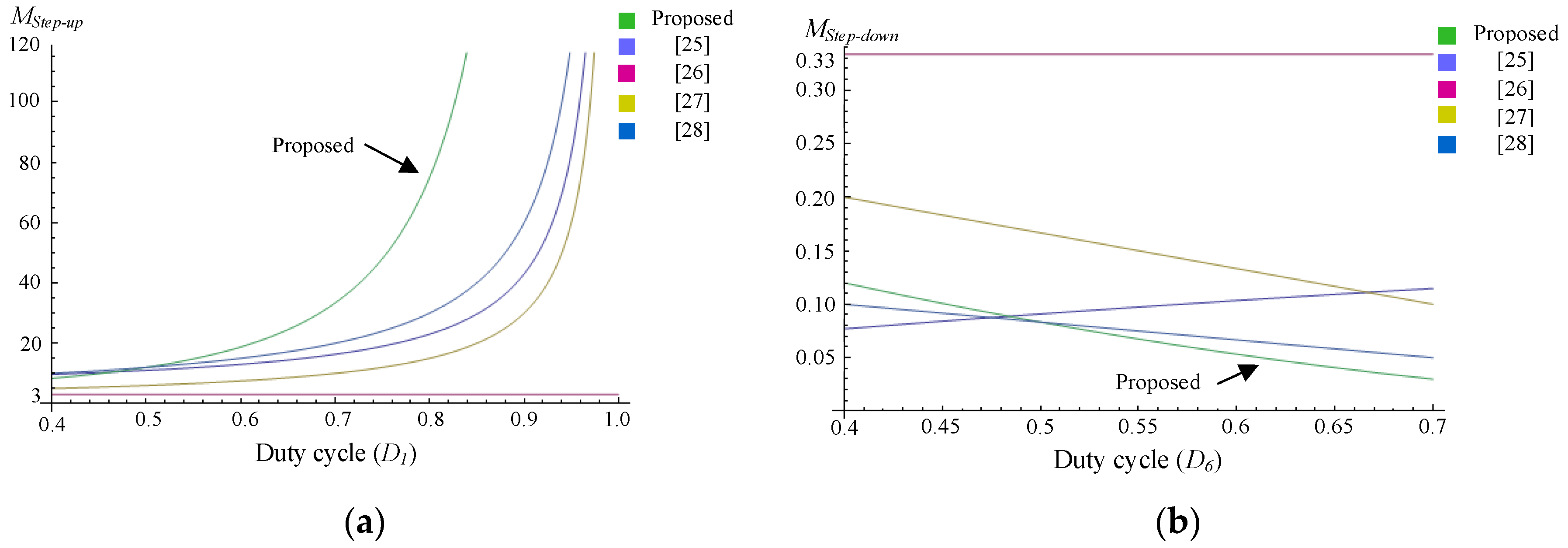
| Voltage conversion ratio in step-up mode (VH/VL) | [(1 + n)/(1 − D)] + n | n | n/(1 − D) | 2n/(1 − D) | [n(1 + D1 − D3)]/[(1 − D1)(1 − D3)] |
| Voltage conversion ratio in step-down mode (VL/VH) | D/(1 + n + nD) | 1/n | (1 − D)/n | (1 − D)/2n | (1 − D6)2/n |
| Output power | 200 W | 500 W | 1 kW | 1.5 kW | 1 kW |
| Number of MOSFETs | 5 | 8 | 4 | 8 | 6 |
| Number of diodes | 0 | 0 | 2 | 0 | 0 |
| Number of inductors | 0 | 1 | 1 | 0 | 1 |
| Number of coupled inductors | 1 | 1 | 1 | 2 | 1 |
| Number of capacitors | 3 | 1 | 4 | 5 | 4 |
| Full-load efficiency (Step-up/step-down) | 93%/90% | 92.4%/91.7% | 85%/89% | 96.5%/95.8% | 94.1%/91% |
© 2017 by the authors. Licensee MDPI, Basel, Switzerland. This article is an open access article distributed under the terms and conditions of the Creative Commons Attribution (CC BY) license ( http://creativecommons.org/licenses/by/4.0/).
Share and Cite
Shen, C.-L.; Shen, Y.-S.; Tsai, C.-T. Isolated DC-DC Converter for Bidirectional Power Flow Controlling with Soft-Switching Feature and High Step-Up/Down Voltage Conversion. Energies 2017, 10, 296. https://doi.org/10.3390/en10030296
Shen C-L, Shen Y-S, Tsai C-T. Isolated DC-DC Converter for Bidirectional Power Flow Controlling with Soft-Switching Feature and High Step-Up/Down Voltage Conversion. Energies. 2017; 10(3):296. https://doi.org/10.3390/en10030296
Chicago/Turabian StyleShen, Chih-Lung, You-Sheng Shen, and Cheng-Tao Tsai. 2017. "Isolated DC-DC Converter for Bidirectional Power Flow Controlling with Soft-Switching Feature and High Step-Up/Down Voltage Conversion" Energies 10, no. 3: 296. https://doi.org/10.3390/en10030296