1. Introduction—The Kelvin-Source Terminal
Faster switching semiconductors mean that the parasitic elements of packaging materials impact semiconductor performance to a greater degree. This is particularly the case when utilizing wide bandgap semiconductors, which can switch several hundred volts and several tens of amperes in a few nanoseconds.
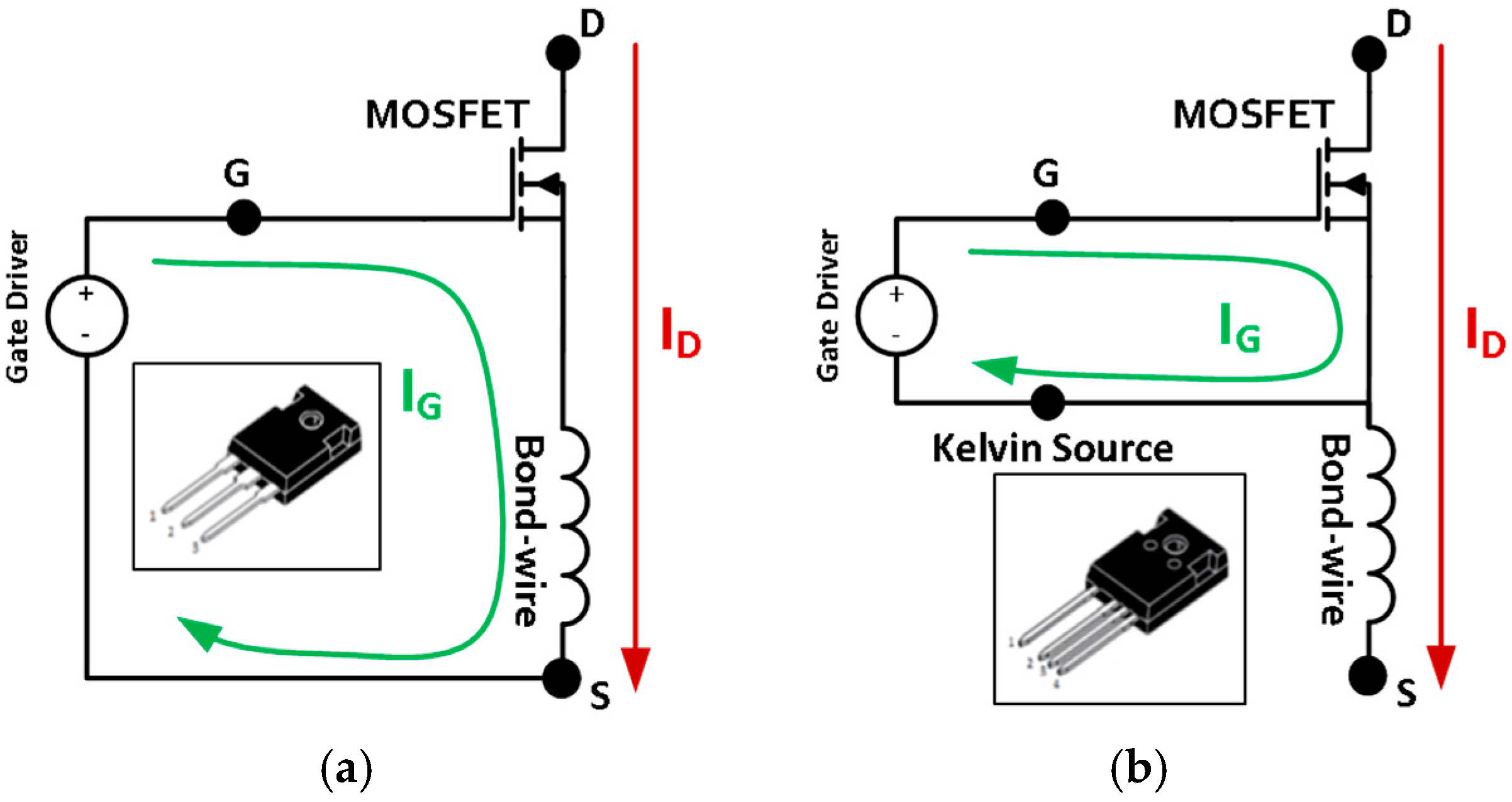
As a consequence of these switching speeds, the use of a fourth terminal known as a kelvin-source (or emitter in insulated gate bipolar transistors, IGBTs) connection to provide the reference potential for the gate control voltage is becoming more common. This technique essentially separates the current path of the control signal and the path of the load current from drain to the source (or collector to emitter in IGBTs).
Figure 1 demonstrates the above principle. In the traditional three-terminal arrangement (
Figure 1a), the fast drain current transient during switching causes a voltage drop across the common parasitic inductance of the source bond-wires. This induced voltage is in opposition to the driving voltage, and consequently slows down the switching transient and increases energy loss [
1,
2]. To avoid the common source inductance, an additional terminal known as the kelvin-source is used, as shown in
Figure 1b.
It is the objective of this article to focus on how the kelvin-source terminal can also be utilised for condition monitoring purposes. The article performs experiments on Silicon Carbide (SiC) MOSFETs, however the same principle can also be applied to Silicon IGBTs provided that they contain a kelvin-emitter terminal.
2. Background: Reliability and Condition Monitoring of Power Semiconductors
The reliability of power semiconductor devices is an important issue, since their unexpected failure can lead to significant downtime of power converters. This downtime can incur significant economic costs in applications such as renewable power. Additionally, the economic costs of power device failures in applications such as military, aerospace, and transport can equal the total cost of the entire system, as such failures can cause catastrophic and unrecoverable effects [
3].
If failures can be anticipated, the operation of a system can be halted before a catastrophic breakdown occurs, or pre-emptive maintenance scheduled that reduces the total downtime of the system. Nevertheless, the anticipation of failures in power semiconductors is difficult.
Power semiconductor reliability is significantly influenced by junction temperature and temperature cycling conditions. Failure mechanisms are generally separated into two categories: die-related failure mechanisms and package-related failure mechanisms. Wu et al. [
4] define die-related failure mechanisms with two further groupings: short-circuit and open-circuit failures.
On the topic of condition monitoring and failure prediction, the most studied failure mechanisms appear to be associated with the packaging materials. Here, the failures are primarily attributed to the differences in the coefficients of thermal expansion of the various materials of the semiconductor die and package construction, combined with the temperature swings they experience [
5]. Repeated thermal cycling then leads to thermo-mechanical stress that results in the gradual wear-out of the packaging materials. The most pertinent issues are lift-off and cracking of the bond-wires that connect the semiconductor die to the terminals of the power module, and fatigue in the solder joints which reduces the effective area for heat to escape via conduction from the die through the baseplate [
6].
The development of condition monitoring systems for power semiconductor modules has been an active research area in the past decade [
6,
7,
8]. The majority of research has focused on monitoring an electrical parameter that indicates degradation. Examples of the most commonly monitored parameters are: the forward voltage in IGBTs (or the on-state resistance in MOSFETs) [
9,
10,
11] and the evolution of a module’s thermal resistance (R
th) [
12,
13,
14,
15,
16]. These parameters have been studied since the 1990s.
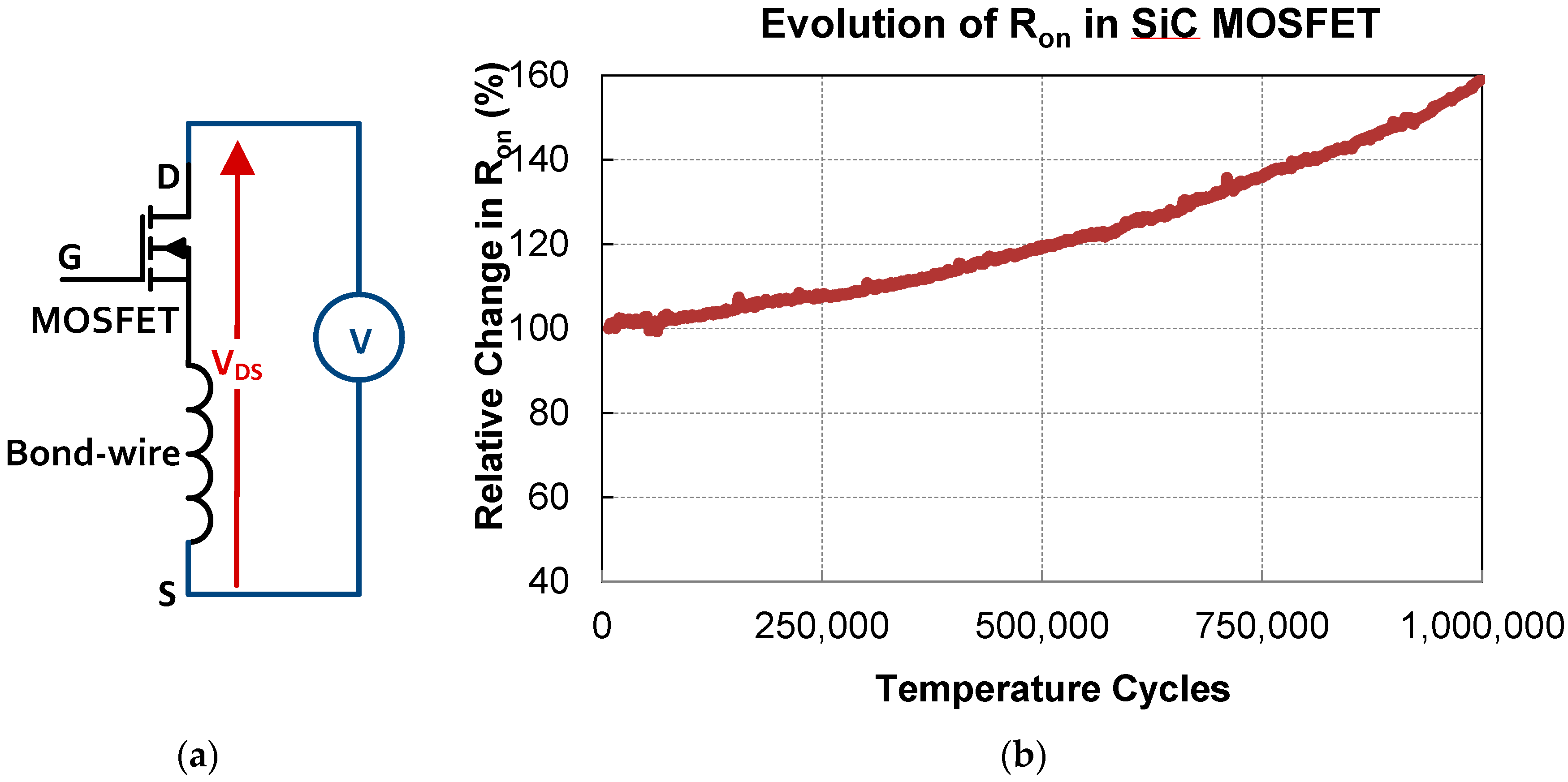
While the above indicators readily observe degradation in laboratory conditions, they are ultimately influenced by numerous failure mechanisms. As such, it is challenging to incorporate them into real-world condition monitoring systems, since it is difficult to ascertain with a high degree of certainty whether a critical level of degradation is present. This is especially the case for the forward voltage of an IGBT or the on-resistance of a MOSFET, which is influenced by both die- and packaging-related failure mechanisms. The reason for this is shown in
Figure 2a: any measurement of the voltage drop across a MOSFET or IGBT includes the voltage drop of both the semiconductor die and the bond-wires. Therefore, when observing an increase in the on-state resistance of a MOSFET (e.g., as in
Figure 2b), it is not possible to determine what the cause is without performing additional after-failure analysis.
In fact, the forward voltage can be affected by several conditions: junction temperature, gate oxide integrity, bond-wire fatigue, surface metallization reconstruction, or a faulty gate driver. This is perhaps why there are a variety of aging trends reported in the literature when examining the forward voltage of a device. For example, increases in the forward voltage in IGBTs of 5%, 7%, and 20% have been reported before module failure occurs [
7,
9,
11,
15]. At the same time, decreases of up to 25% were present in other studies [
7,
16,
18]. Data for MOSFETs are harder to compare since the majority of reliability studies seem to be performed on IGBTs. However, increases in the region of 40% to 60% can generally be seen in previous literature [
17,
19,
20].
Although the forward voltage of a device is influenced by numerous degradation conditions, it is still an attractive parameter to monitor, since it is relatively easy to extract during power semiconductor operation [
21].
The pressing question, therefore, is: at which point does the monitored parameter reliably signify the end-of-life condition of the device, so that operation can be halted and a catastrophic failure prevented?
One tactic to simplify the process of determining when the forward voltage displays a critical level of degradation would be to reduce the number of degradation conditions it is dependent on. This is difficult in a traditional three-terminal device. However, for devices with an auxiliary-source connection, this article will demonstrate a simple measurement circuit with which degradation in the semiconductor and bond-wires can be monitored separately.
A review of past literature does not yield many results of past publications that have studied the use of the auxiliary-source (or emitter) connection for condition monitoring purposes. However, one study was performed by Farokhzad et al. in 1996 [
22,
23]. This study was performed on IGBTs, and an additional current source was used to inject a sensing current (independent of the load current) between the power-emitter and auxiliary-emitter. The key difference in this article is that the resistance between the power-source and auxiliary-source is evaluated while the device is in the on-state, and no additional current source is used.
3. Results
3.1. On-State Voltage Monitoring with Kelvin-Source Connection
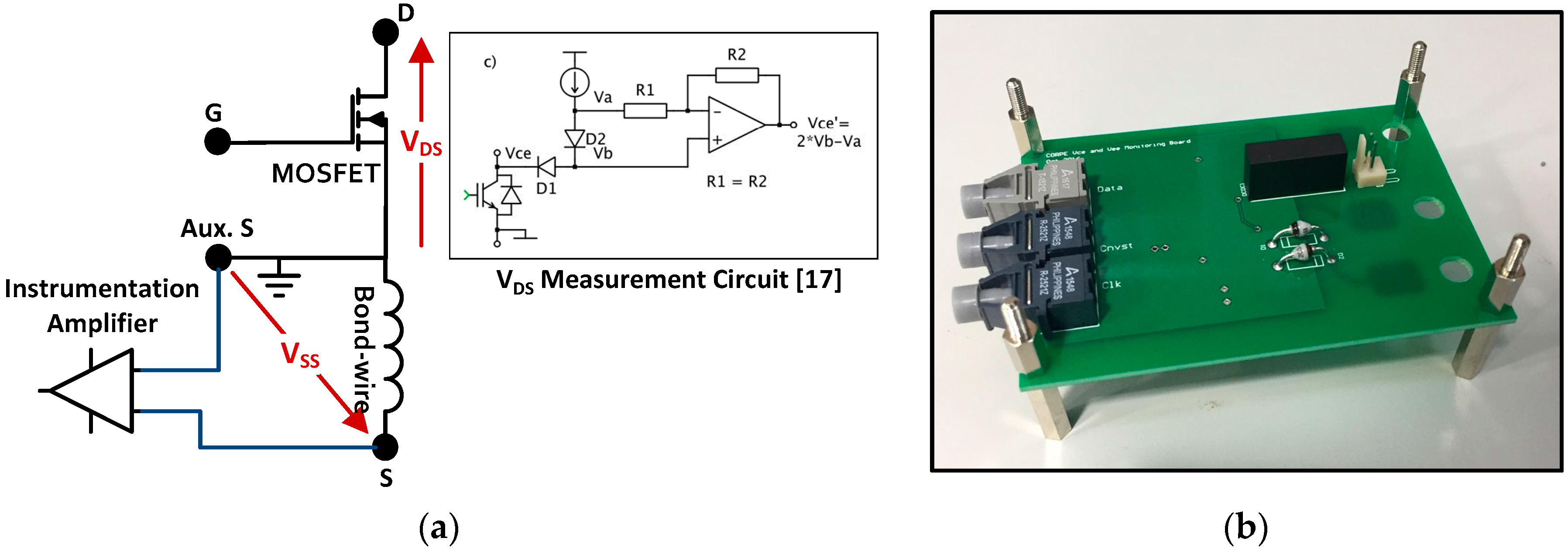
The principle of the on-state measurements in this article are shown in
Figure 3. The kelvin-source connection is used as the ground reference for two voltage measurements. The first measurement is of the drain to kelvin-source voltage (V
DS). Here, the measurement circuitry from [
17] is used, which uses a blocking diode to protect the measurement amplifier circuit against high voltages when the MOSFET/IGBT is in the off-state. The second measurement—of the kelvin-source to source voltage (V
SS)—uses only an LT1167 instrumentation amplifier, since this does not experience the high voltage of the drain terminal. The outputs of the two amplifiers are connected to a 14-bit two-channel Analogue-to-Digital Converter (ADC): an AD7367. The presented measurement circuit can be used for both high and low side switches.
As can be seen from
Figure 3a, the V
DS measurement covers only the voltage drop across the semiconductor, while V
SS measures the voltage drop solely across the bond-wires and the surface metallization. Therefore, it would be logical to assume that a fault in the semiconductor (V
DS) would have no impact on V
SS, and vice-versa. We conducted two experiments to test this hypothesis: one to emulate a semiconductor side-related failure, and another to induce a bond-wire failure.
The following experiments are performed on SiC MOSFETs, which were chosen purely because of the prevalence of a kelvin-source connection in these devices. It should be noted that the primary objective of this article is to demonstrate a proof-of-concept that the described measurement circuit has the ability to monitor semiconductor and bond-wire degradation separately. Therefore, the article does not focus on the analysis of failure mechanisms specific to SiC devices—the experiments could have equally been performed on silicon IGBTs.
3.2. Gate Driver Voltage Failure
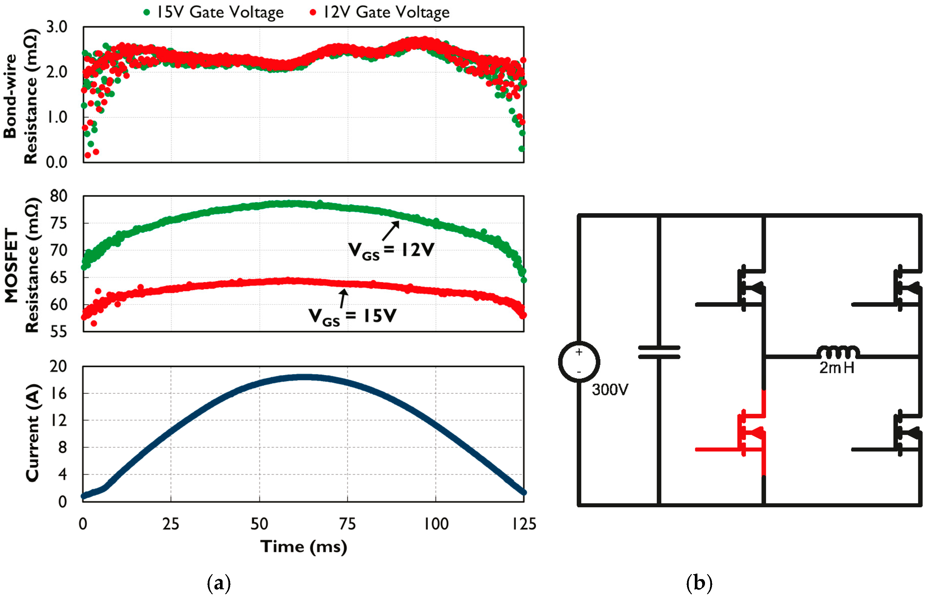
The first experiment involved the emulation of a gate driver failure. Here, the objective is to induce a fault in the semiconductor side, while leaving the bond-wires in a healthy state. Additionally, the experiment helped to verify that the measurements of both VDS and VSS could be performed in full switching conditions.
To do this, we operated four 4L-TO247 packaged SiC MOSFET devices (Wolfspeed C3M0120100K, Cree Inc., Durham, NC, USA) in an H-Bridge inverter, and varied the gate driver voltage from the recommended 15 V, to a “faulty” condition of 12 V. The inverter had a switching frequency of 7.5 kHz, with the load current at a frequency of 4 Hz. The resistances of both the bond-wires and the MOSFET die (calculated using V
SS and V
DS, respectively) for one device during one sinusoidal half-period are shown in
Figure 4. The current was measured using a LEM 55-P current transducer.
It can be seen that there was a large variation in the MOSFET resistance depending on the gate voltage used. The MOSFET resistance was around 10 mΩ higher when the gate voltage was lowered to 12 V. This result is logical, as the reduction in gate voltage reduces the charge in the inversion layer, and the MOSFET resistance is consequently increased. At the same time, the resistance of the bond-wires showed no significant change with respect to the gate voltage.
3.3. Accelerated Aging Test with 20 A Silicon Carbide MOSFETs
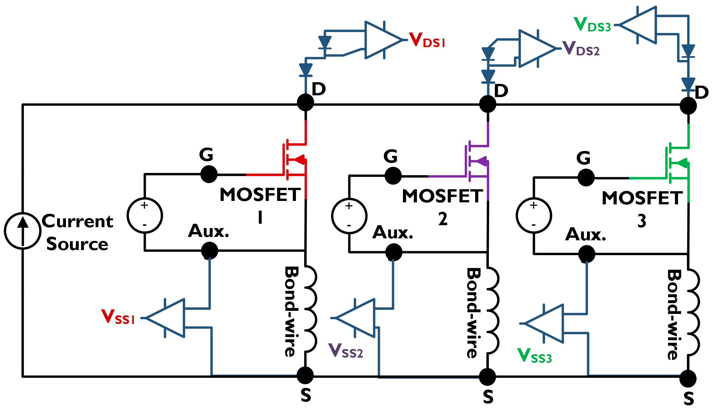
The second experiment performed was an accelerated aging test of three 20 A SiC MOSFETs. The three MOSFETs were from a single six-pack module (Wolfspeed CCS020M12CM2, Cree Inc., Durham, NC, USA). The MOSFETs were aged using a traditional constant current power cycling test, where thermal fatigue is induced through repetitive self-heating and cooling phases. The objective for this test was to induce bond-wire degradation.
Figure 5 displays the basic schematic for the test, while
Table 1 shows the test parameters. A constant current of 22.5 A is injected sequentially through each MOSFET for a period of 2 s, with a 0.1 s overlap time. The temperature of each MOSFET was monitored using optical fibers through the module dielectric gel. With the heatsink temperature set to 75 °C, the temperature swing for the hottest MOSFET was around 75 °C, with a maximum temperature of 160 °C.
All three MOSFETs were monitored for V
DS and V
SS using the previously described measurement board, so the resistances of both MOSFET die and the bond-wires could be calculated as the test progressed. A total of 16 measurements were made during each 2 s pulse, with measurements performed every 15 min throughout the duration of the test.
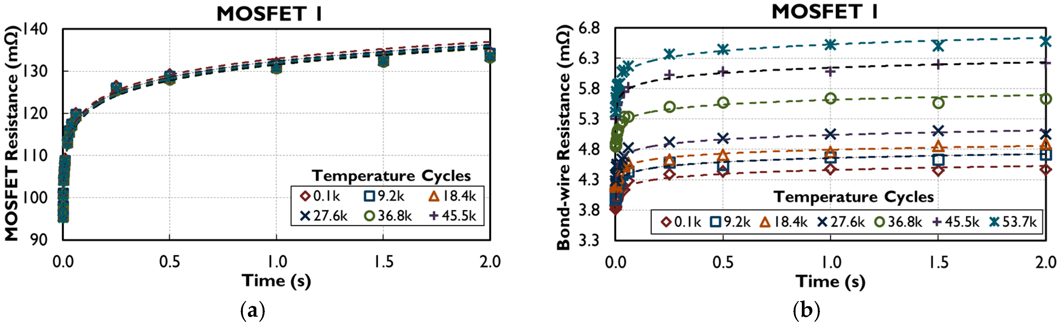
Figure 6 displays an example from MOSFET 1 of how the measurements enabled the tracking of resistances due to self-heating during the 2 s pulse, while also showing how the resistances evolved as the number of temperature cycles increased. From this figure, there is already a clear contrast—the MOSFET resistance appears to be stable throughout the test, while the bond-wire resistance increases by almost 50%.
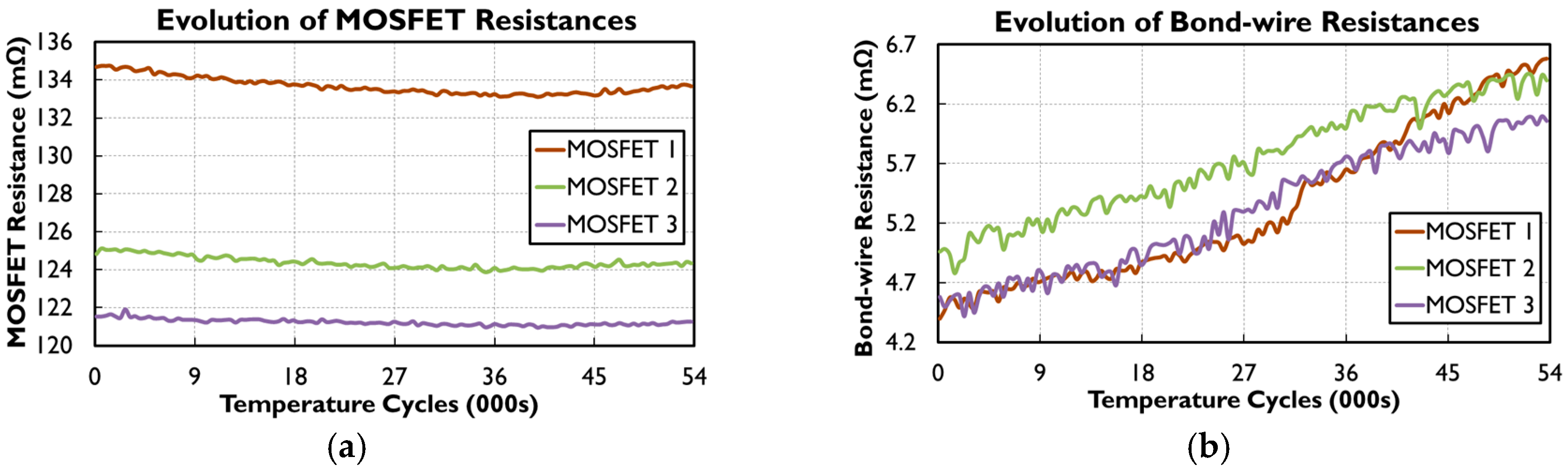
Figure 7 displays the evolution of MOSFET and bond-wire resistances for all three devices. The values on these graphs are taken from the last measurement in the 2 s pulse. It is clear that there are opposing trends: the resistance of the bond-wires in all three devices increases by around 1.5 mΩ, while the MOSFET resistances show a slight decrease of up to 1 mΩ.
MOSFET 1 showed the largest variation in both its MOSFET and bond-wire resistance. Coincidently, MOSFET 1 also had the highest baseline MOSFET resistance of 135 mΩ, and thus had the highest temperature swing. On the other hand, MOSFET 3 showed almost no change in its MOSFET resistance; however, its bond-wire resistance showed an increase consistent with the other two.
4. Conclusions
This article demonstrates a preliminary proof-of-concept for separate condition monitoring of semiconductor and bond-wire degradation in devices with a kelvin-source (or emitter) terminal. The article shows a simple measurement circuit that produces two output voltages that are dependent on the condition of the semiconductor die and of the bond-wires. These output voltages are demonstrated to be independent of each other. That is, a failure in the semiconductor side (e.g., gate driver failure) does not influence the signal for bond-wire status, while degradation in the bond-wires does not influence the signal for semiconductor status. Therefore, the degradation in these components can be monitored separately. The conventional failure precursor—to monitor a single forward voltage—cannot distinguish between semiconductor die or bond-wire degradation.
Future work will include applying the measurement circuit to a statistically significant number of devices, and using the data to more clearly specify critical levels of degradation. Therefore, the risk of false positives when deciding when to halt device operation can be reduced. The method should also be tested on power semiconductors with several semiconductor chips in parallel.


