
Performance Improvement for Two-Stage Single-Phase Grid-Connected Converters Using a Fast DC Bus Control Scheme and a Novel Synchronous Frame Current Controller

Abstract
:1. Introduction
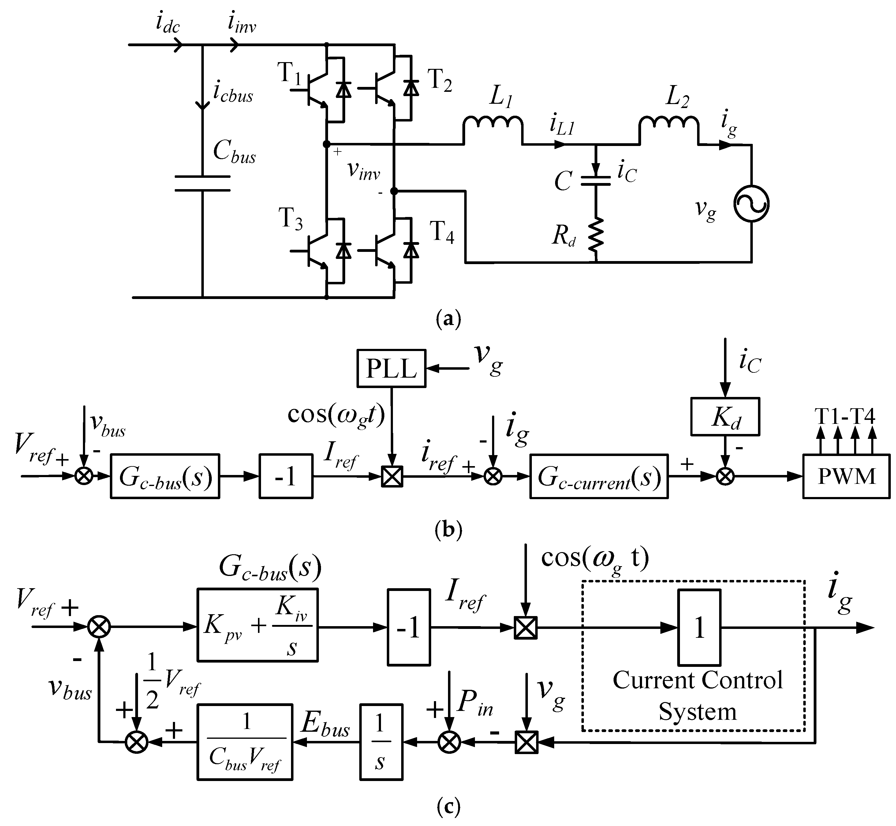
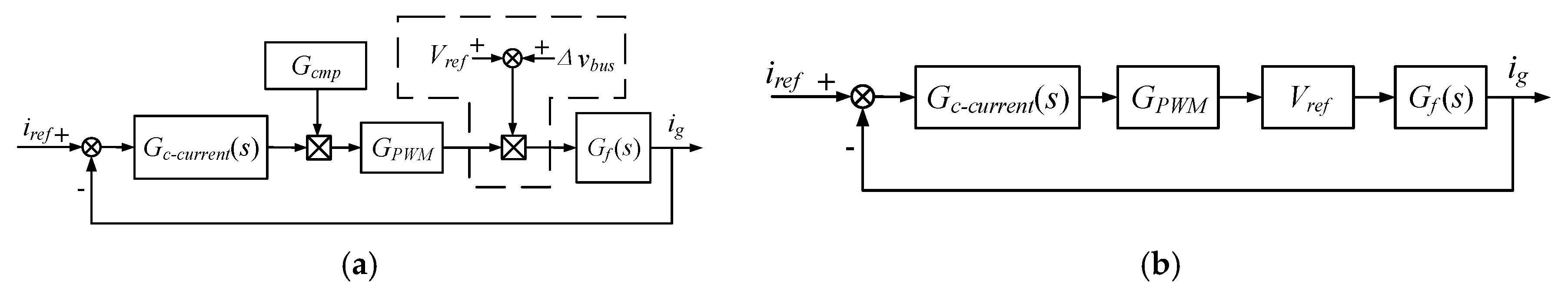
2. Model of an Inverter with a Conventional Control System
2.1. Bus Voltage Control System
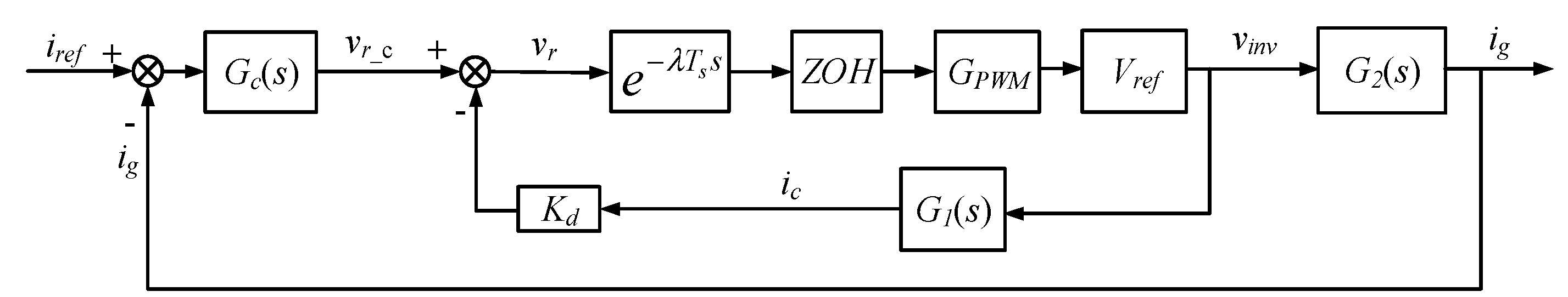
2.2. Grid Current Control System
- (1)
- The 2-f voltage ripple leads to a third harmonic component and a phase shift in the output current. In a similar way, 4-f power pulsation leads to 5th order harmonic current, and so on.
- (2)
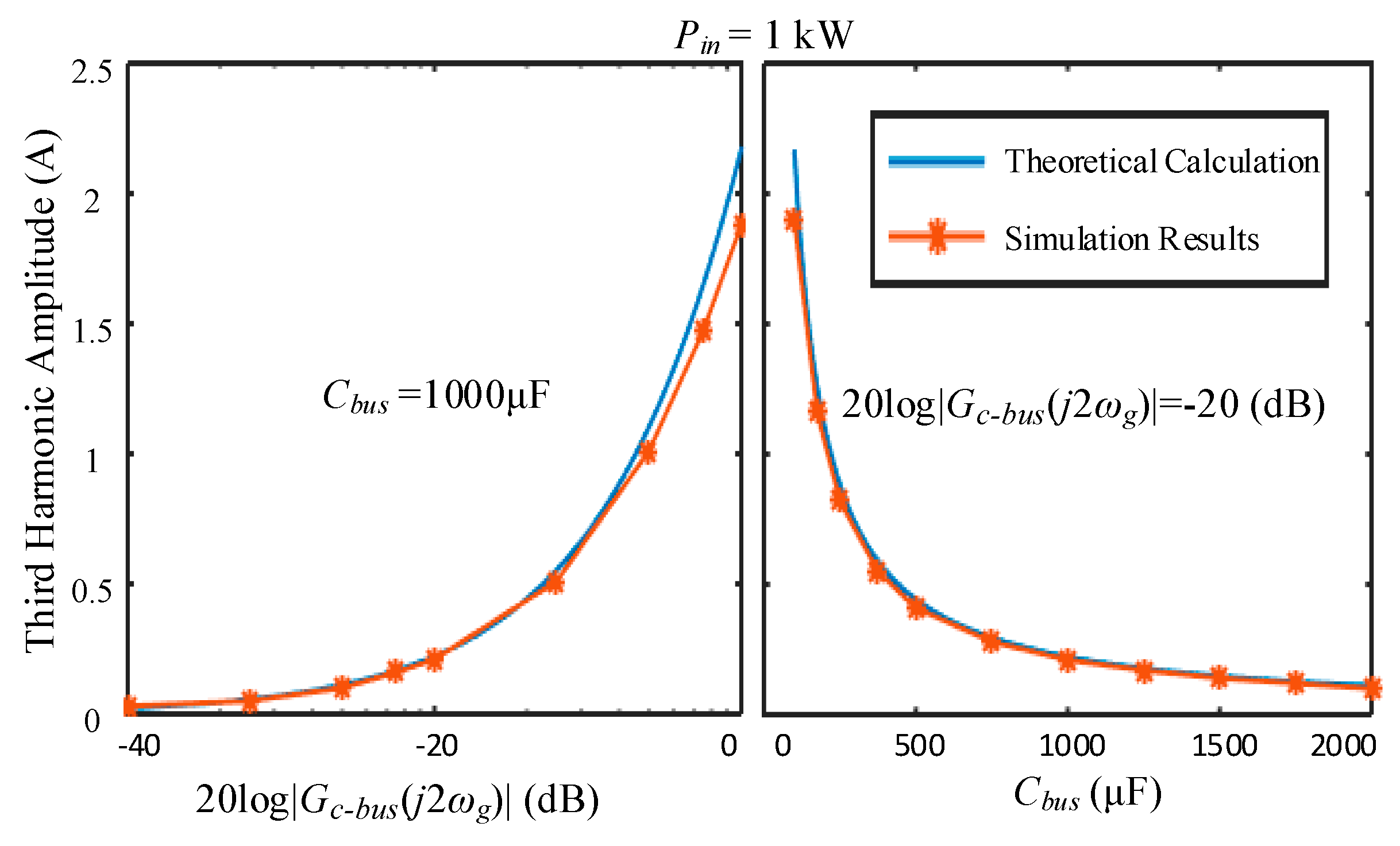
- There is a negative correlation between the harmonic distortion (Ig3) and the bus capacitor value (Cbus). Larger capacitance leads to lower harmonic content, but increases the cost, size and weight of the converter.
- (3)
- There is a positive correlation between the harmonic distortion and the gain of the bus voltage controller (|Gc-bus (j2ωg)|). With a lower gain, there is less distortion in the grid current. However, a low gain may lead to poor transient response or to instability, two properties that are affected by one main parameter, the loop bandwidth. The bus voltage control loop presents a tradeoff between harmonic distortion and bandwidth, which is controlled by the gain of the controller. Thus, a simple PI controller, which is used as bus voltage controller, is unable to address the ripple-caused difficulties.
- (4)
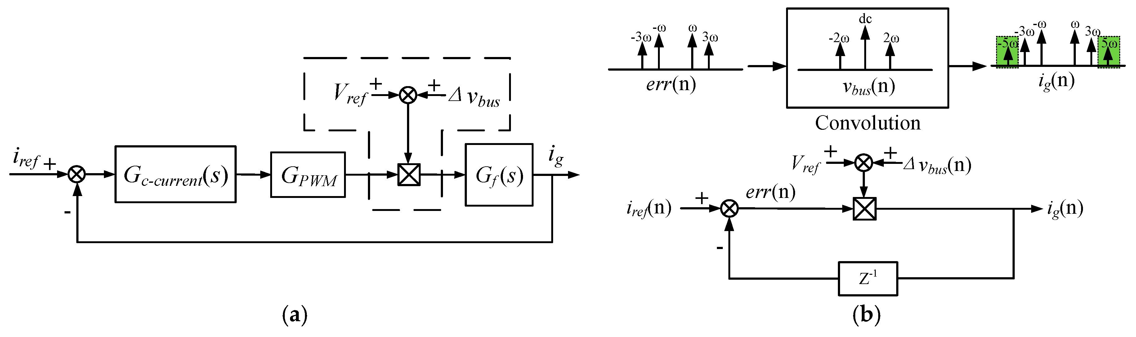
- The 2-f bus voltage ripple also brings about a nonlinear section in the grid current control scheme, which makes contributions to the increase in harmonic component.
3. Proposed Control Scheme
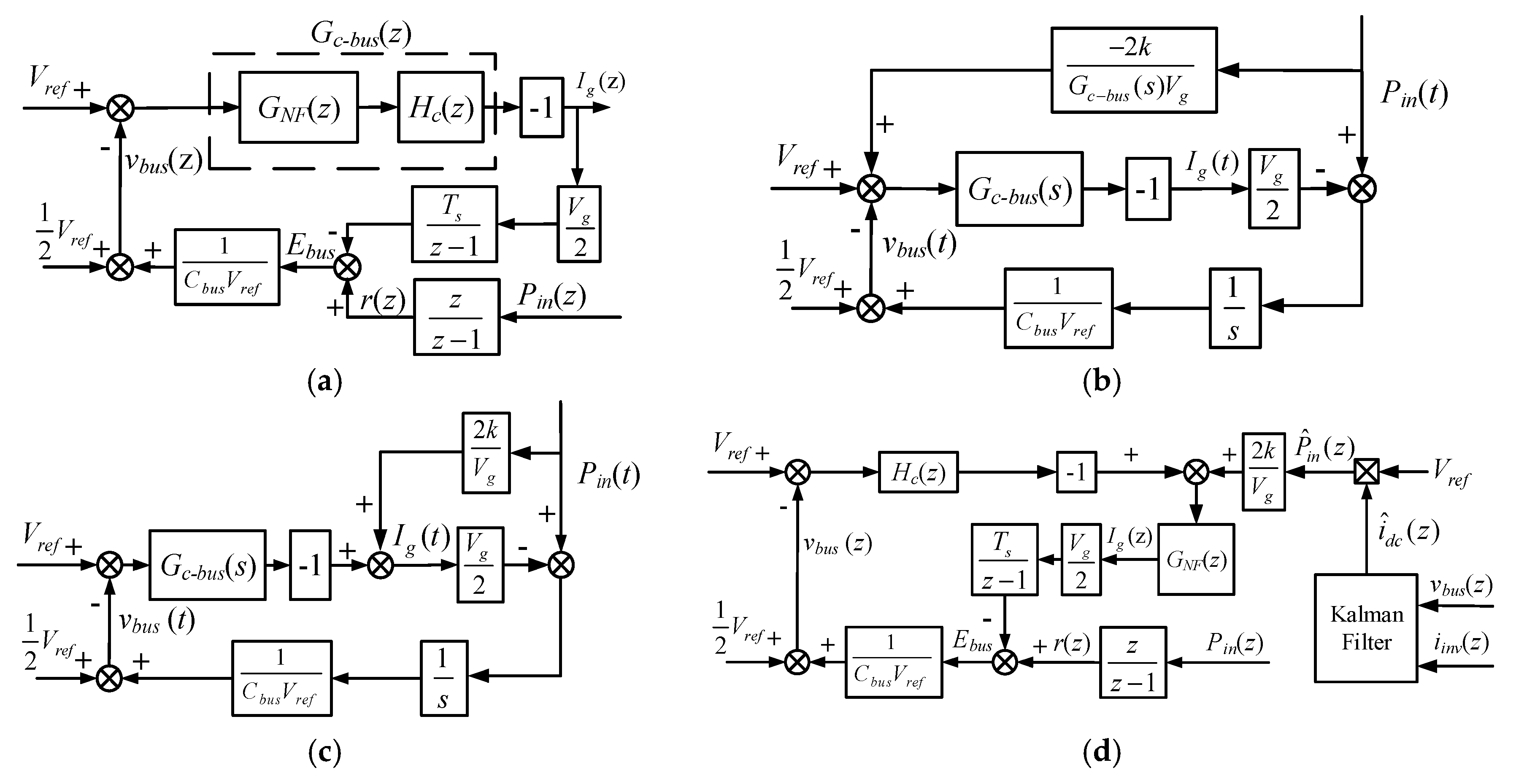
3.1. FIR Notch Filter Inserted Bus Voltage Regulator
3.2. Kalman-Filter-Based Input Power Feedforward
3.3. Modulation Compensation Strategy for Bus Voltage Ripple
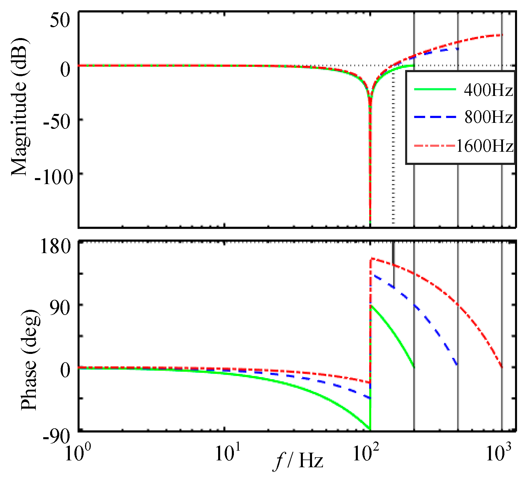
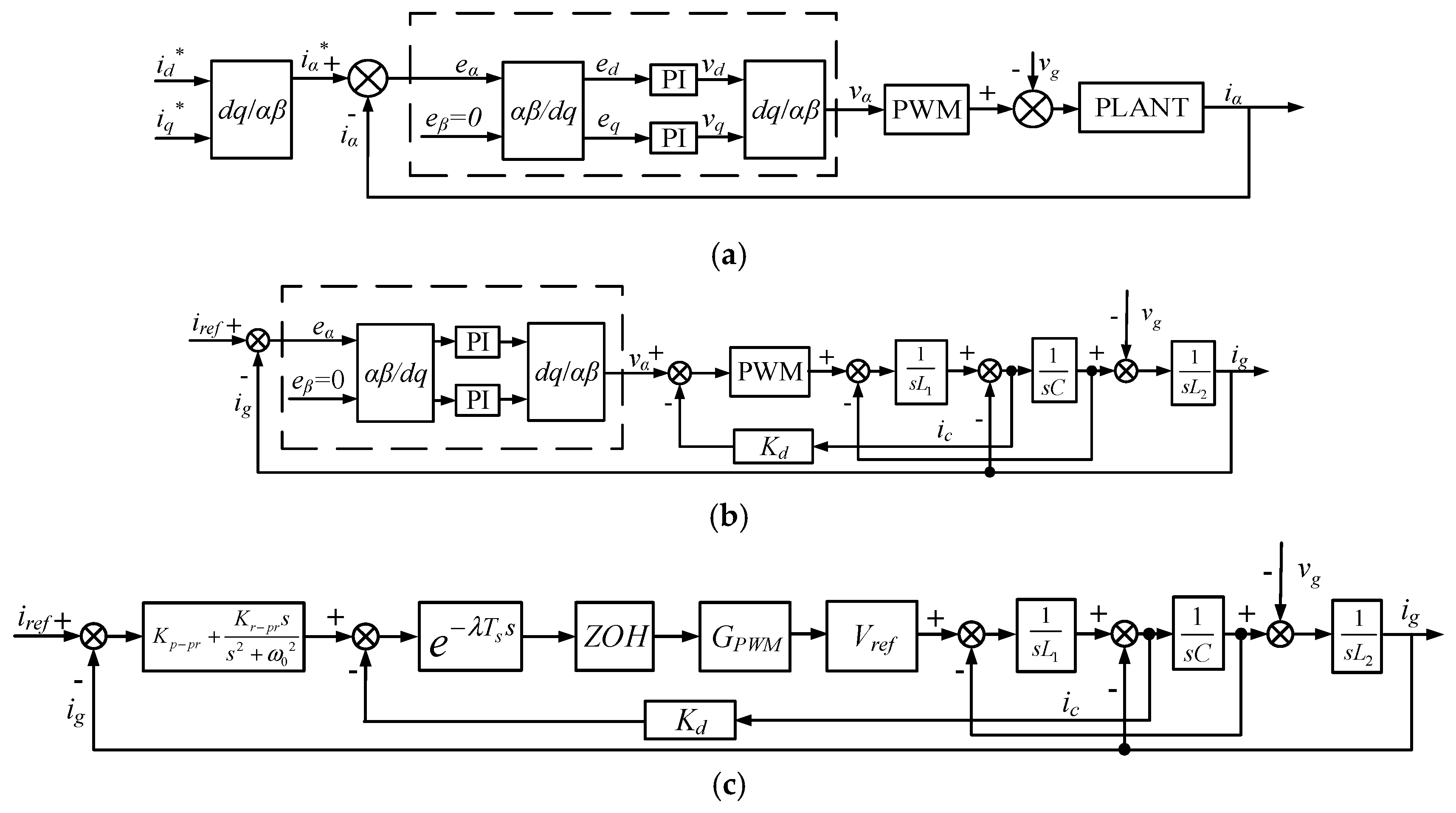
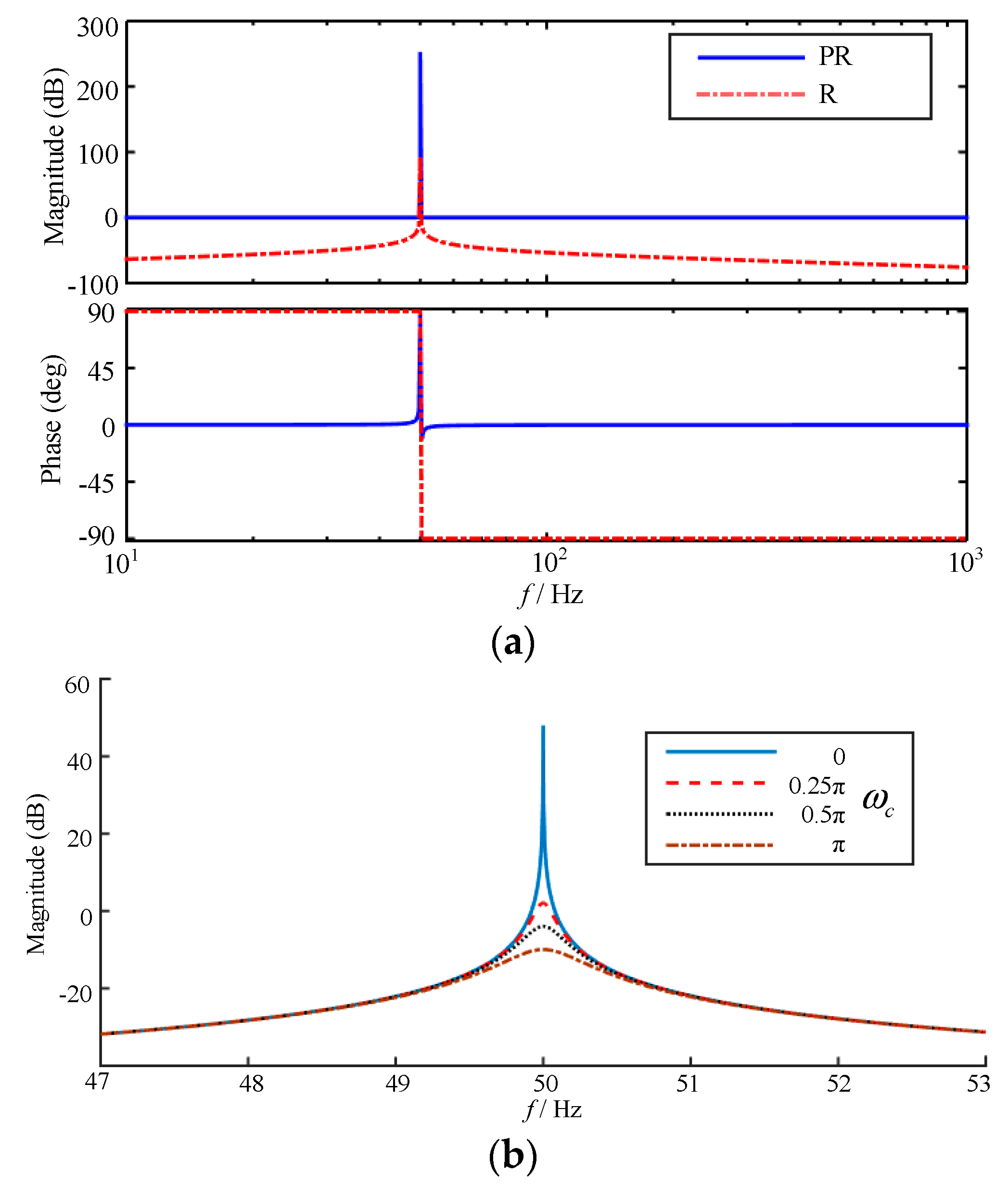
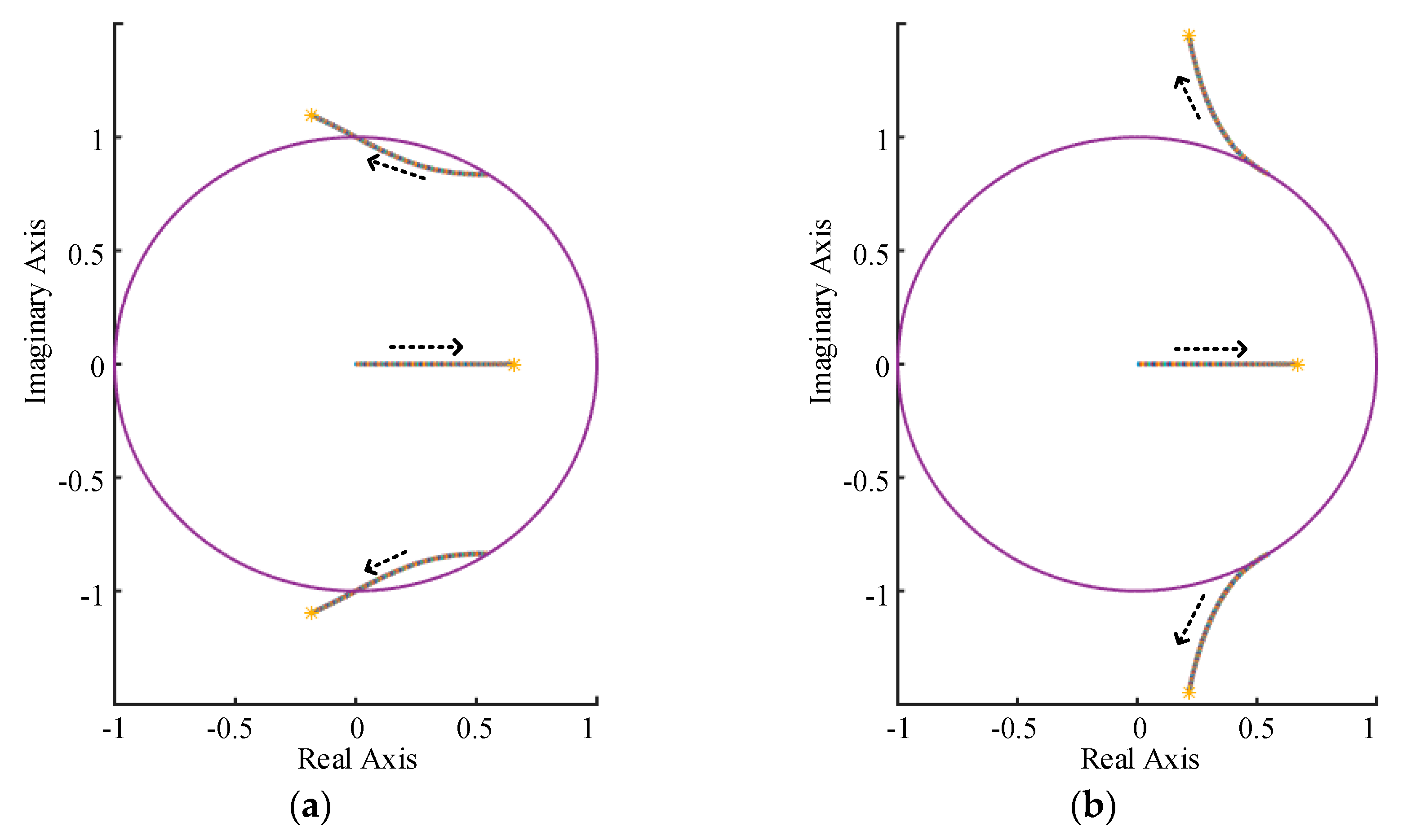
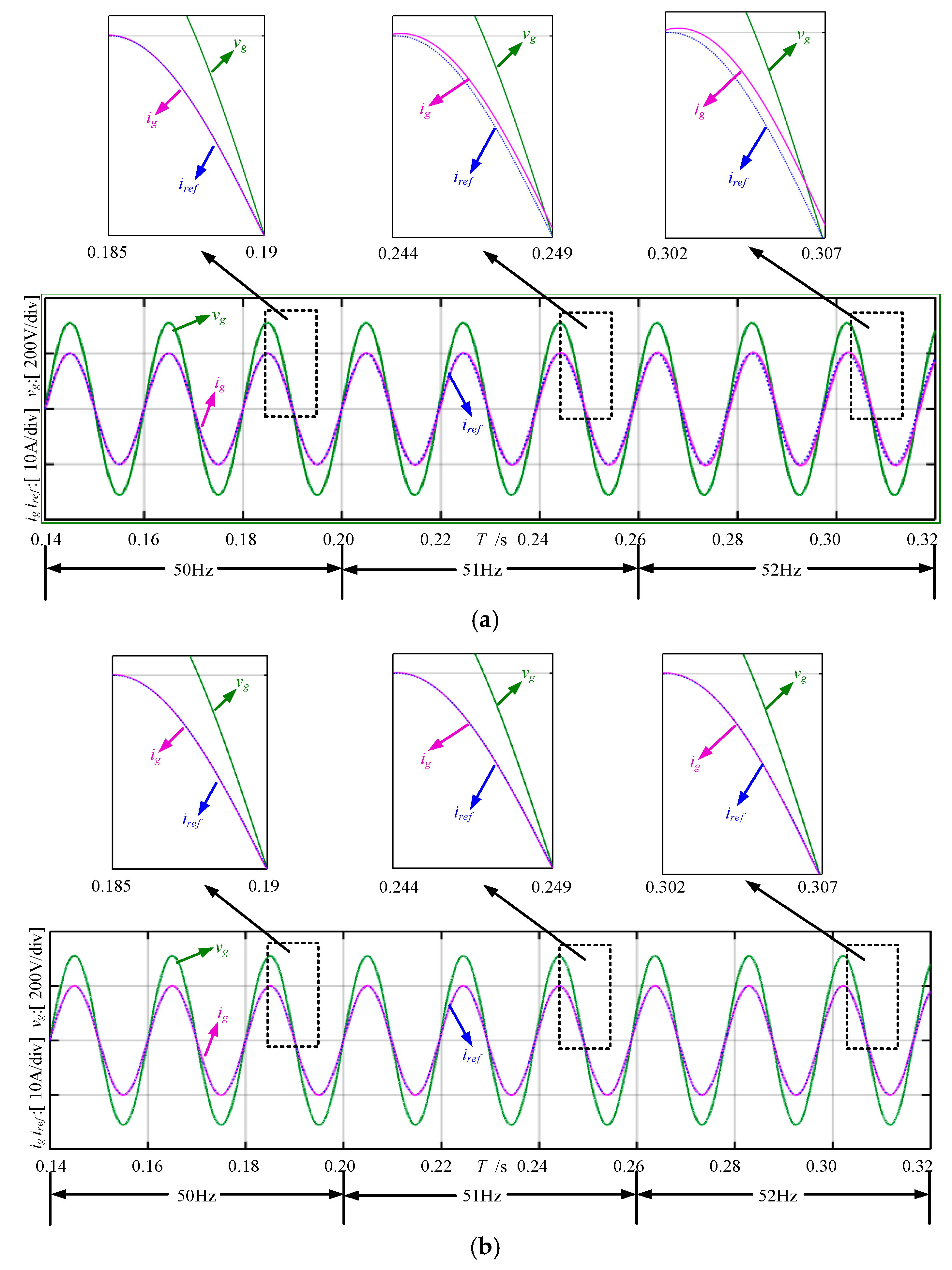
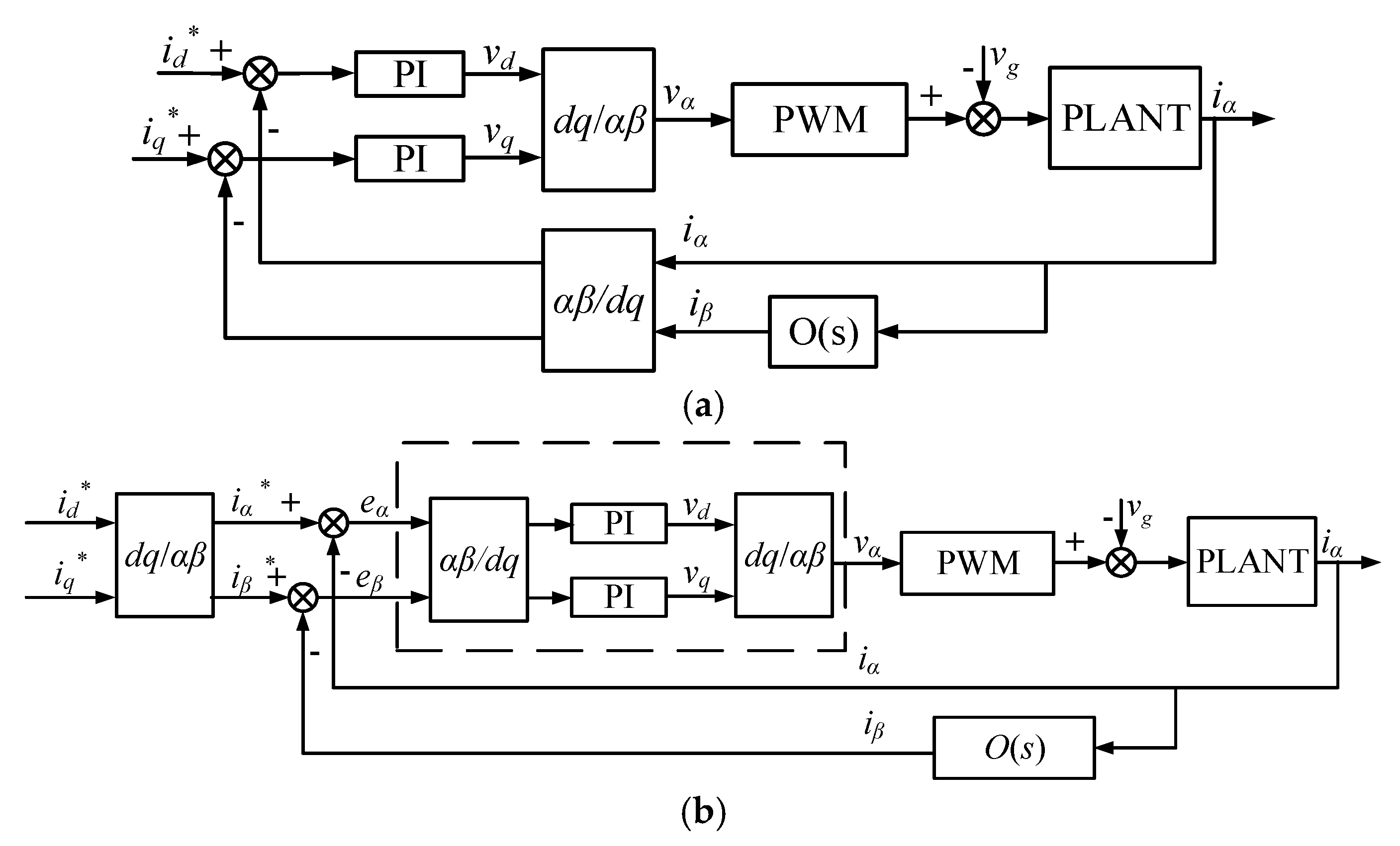
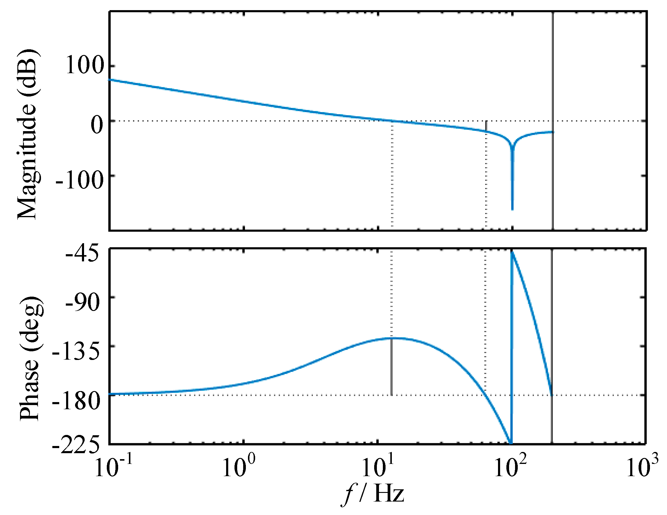
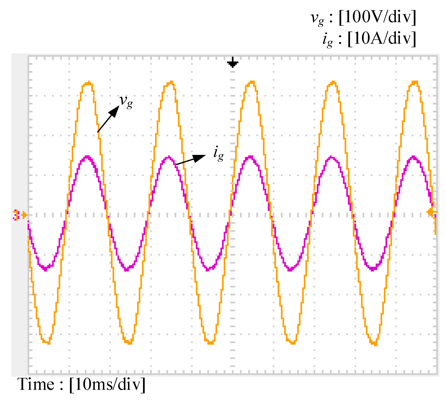
3.4. Novel Synchronous Frame Current Control Scheme for Single-Phase Systems
4. System Design and Simulation
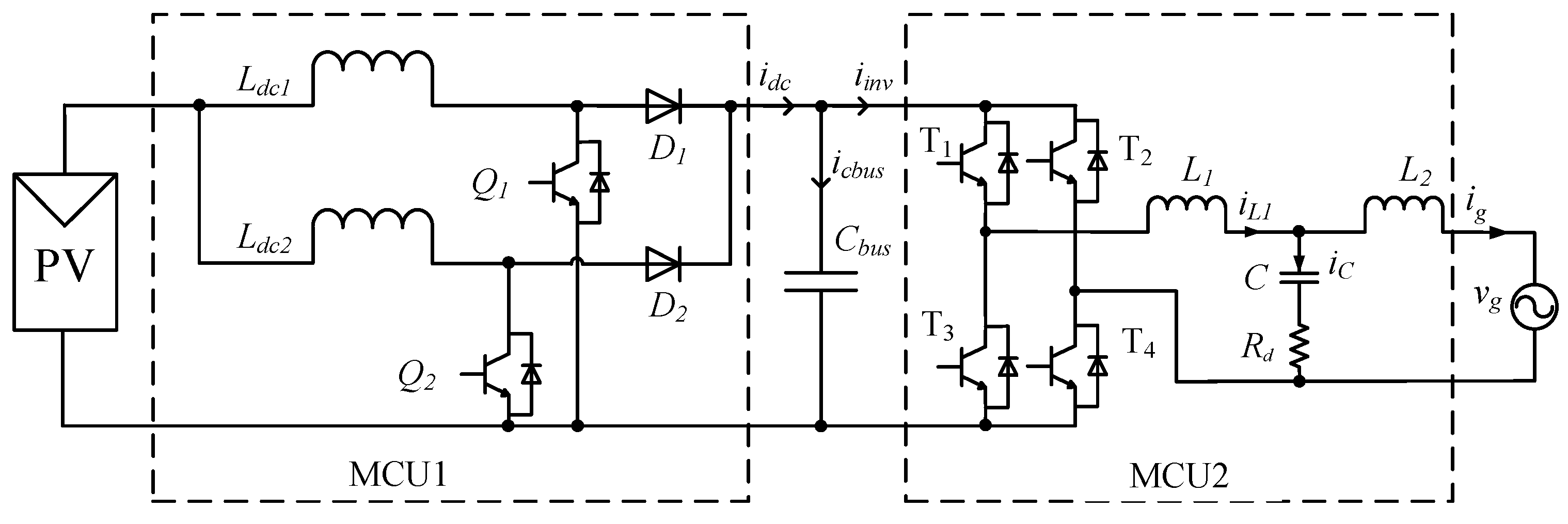
4.1. System Design
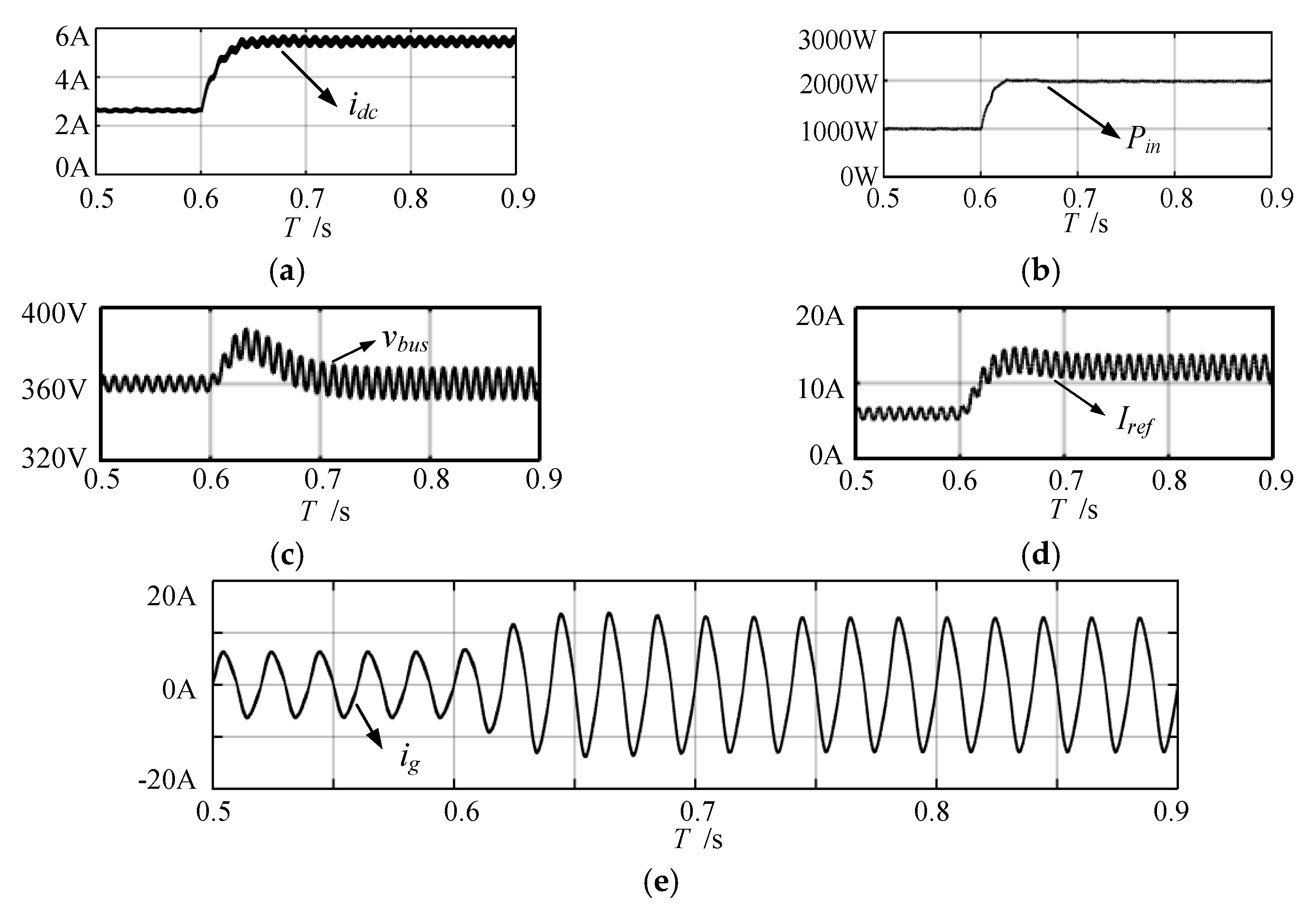
4.2. Simulation
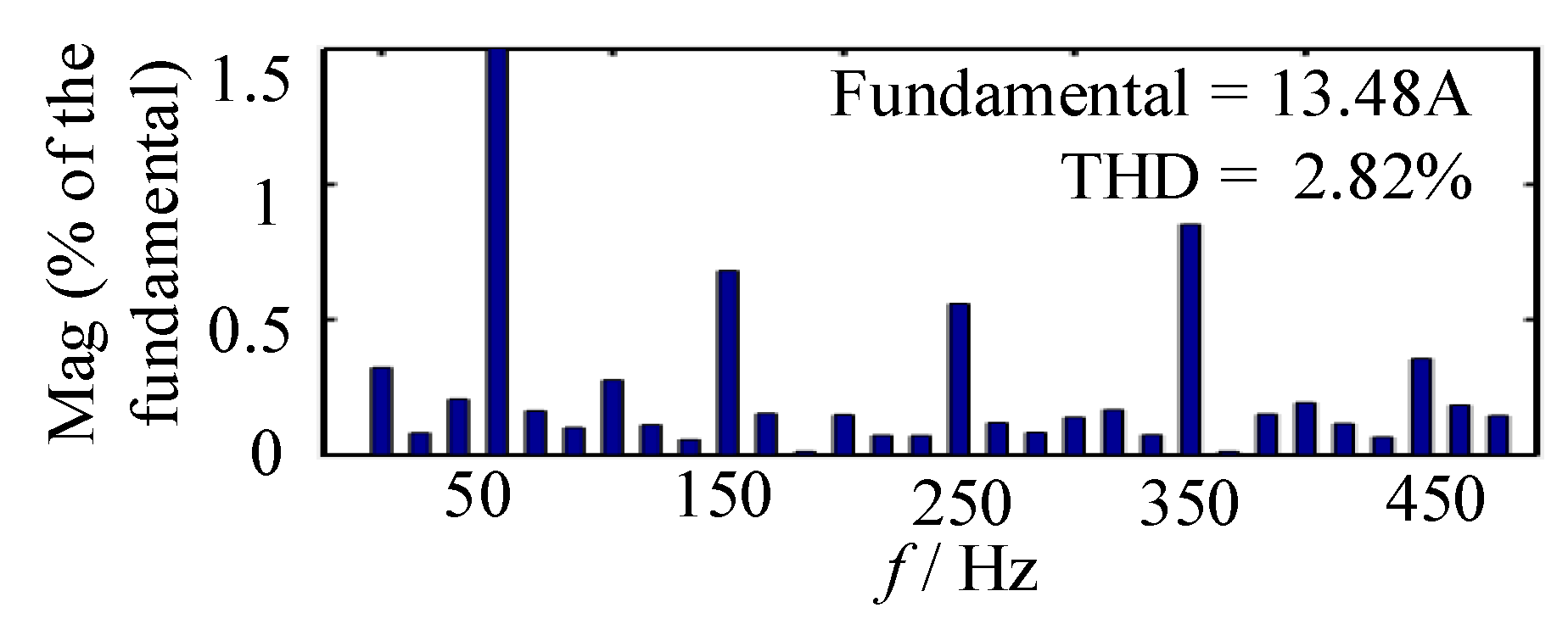
5. Experimental Results
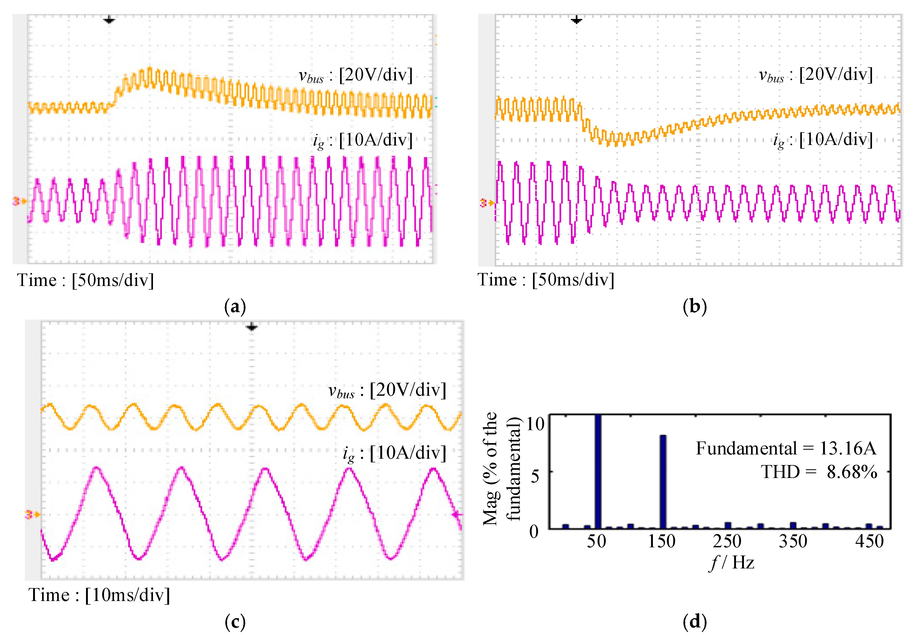
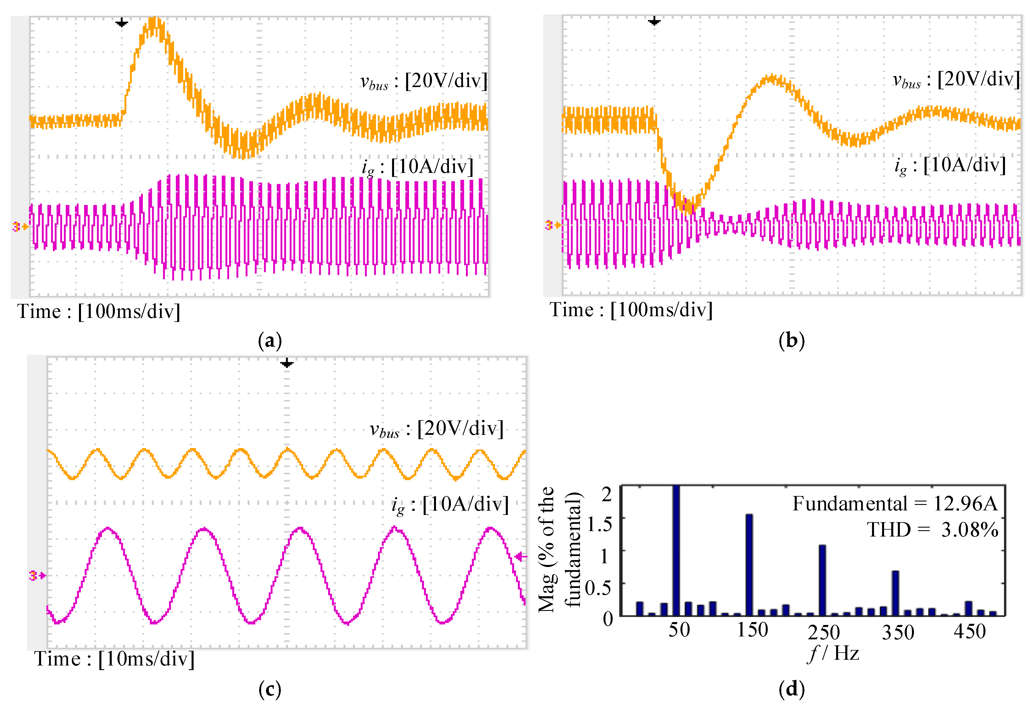
5.1. PI Controller
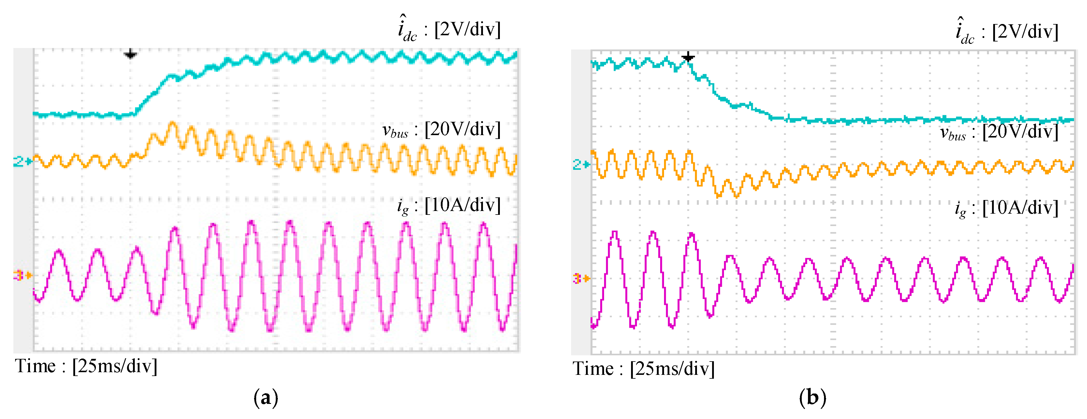
5.2. FIR Notch Filter Inserted Bus Voltage Regulator
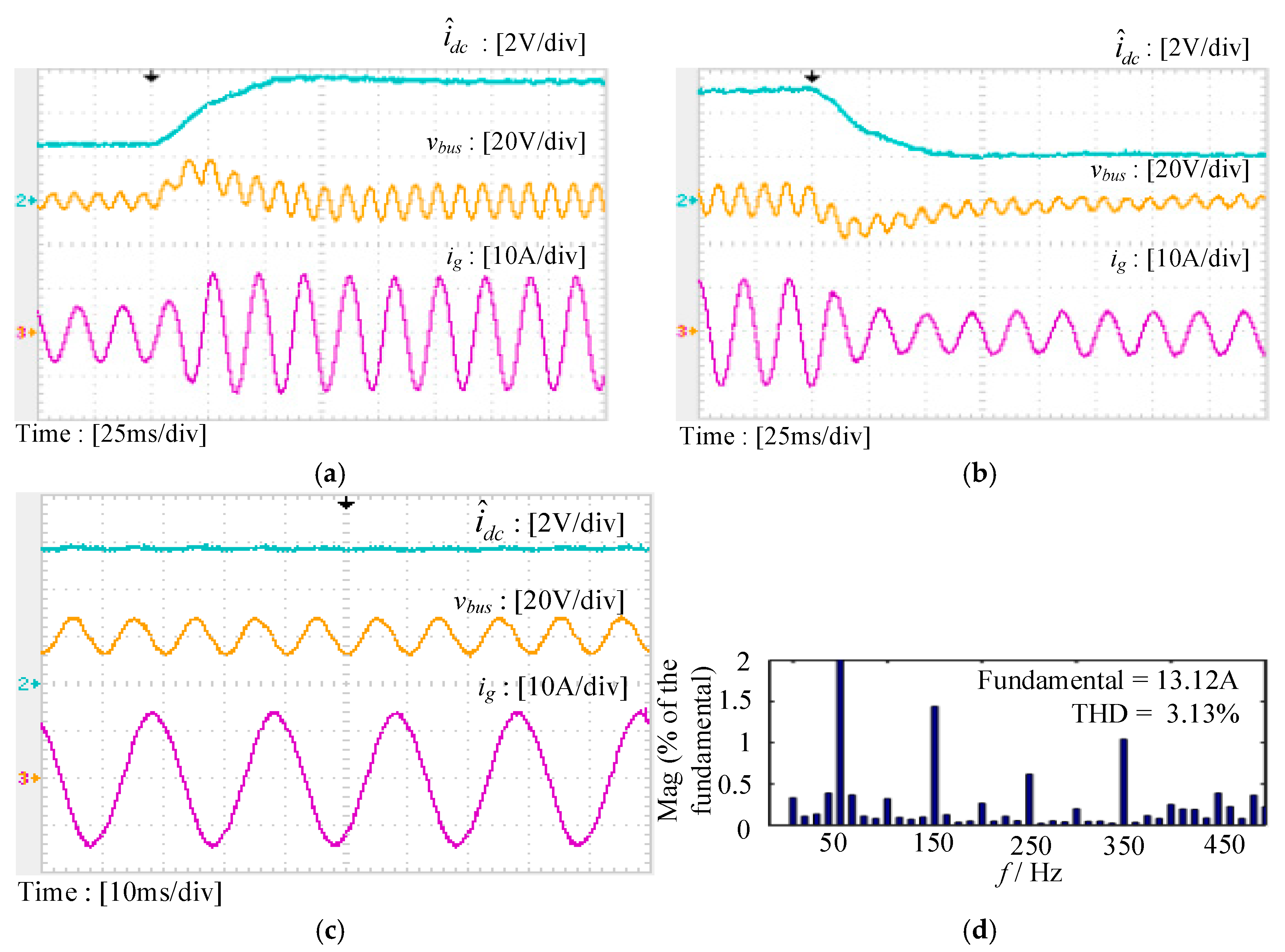
5.3. FIR Notch Filter Inserted Bus Voltage Regulator with Kalman-Filter-Based Input Power Feedforward
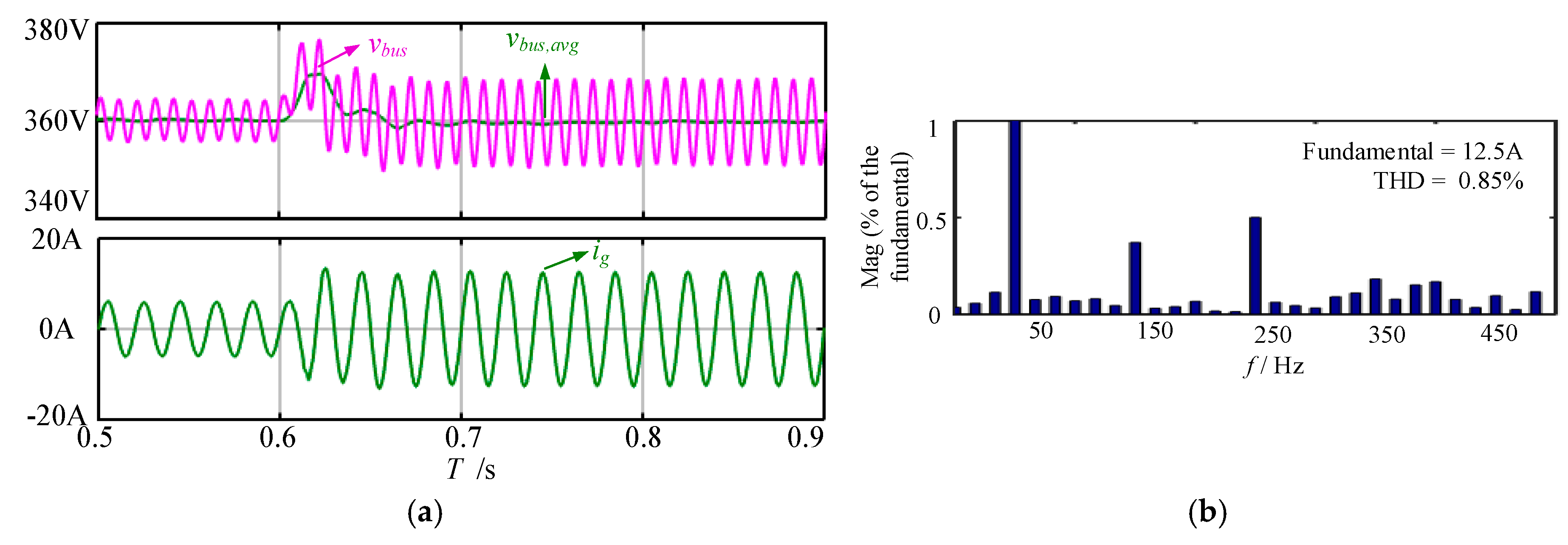
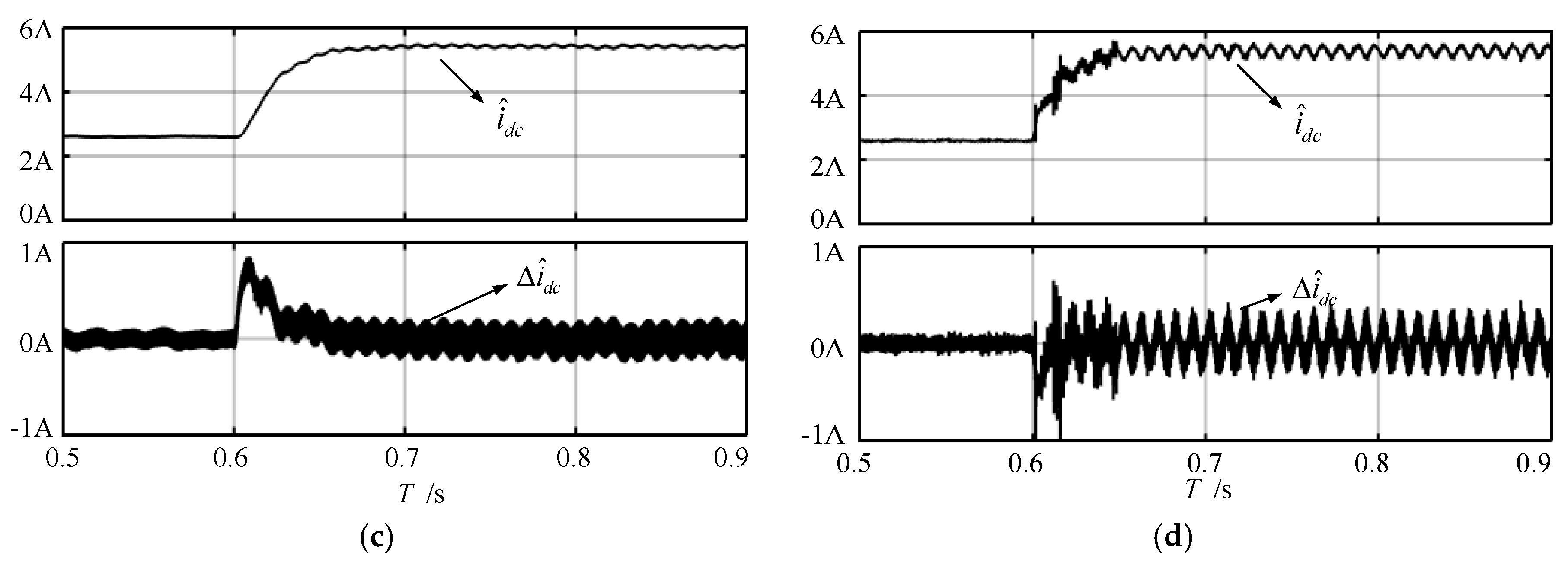
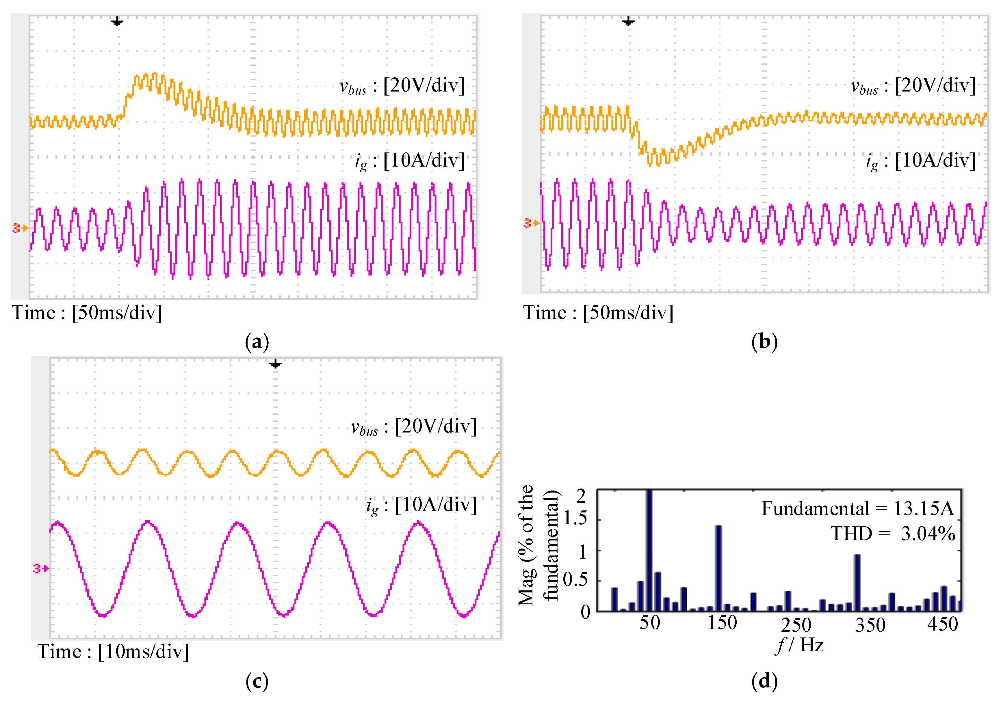
5.4. Modulation Compensation Strategy for Bus Voltage Ripple
6. Conclusions
Acknowledgments
Author Contributions
Conflicts of Interest
Appendix A
References
- Blaabjerg, F.; Teodorescu, R.; Liserre, M.; Timbus, A.V. Overview of control and grid synchronization for distributed power generation systems. IEEE Trans. Ind. Electron. 2006, 53, 1398–1409. [Google Scholar]
- Xia, Y.; Ahmed, K.H.A.; Williams, B.W. A New Maximum Power Point Tracking Technique for Permanent Magnet Synchronous Generator Based Wind Energy Conversion System. IEEE Trans. Power Electron. 2011, 26, 3609–3620. [Google Scholar] [CrossRef]
- Esram, T.; Chapman, P.L. Comparison of Photovoltaic Array Maximum Power Point Tracking Techniques. IEEE Trans. Energy Convers. 2007, 22, 439–449. [Google Scholar] [CrossRef]
- Jeong, H.G.; Kim, G.; Lee, K.B. Second-Order Harmonic Reduction Technique for Photovoltaic Power Conditioning Systems Using a Proportional-Resonant Controller. Energies 2013, 6, 79–96. [Google Scholar] [CrossRef]
- Chen, Y.M.; Chang, C.H.; Wu, H.C. DC-Link Capacitor Selections for the Single-Phase Grid-Connected PV System. In Proceedings of the 2009 International Conference on Power Electronics and Drive Systems (PEDS), Taipei, Taiwan, 2–5 November 2009; pp. 72–77.
- Karimi-Ghartemani, M.; Khajehoddin, S.A.; Jain, P.; Bakhshai, A. A Systematic Approach to DC-Bus Control Design in Single-Phase Grid-Connected Renewable Converters. IEEE Trans. Power Electron. 2013, 28, 3158–3166. [Google Scholar] [CrossRef]
- DeBlasio, R.; Chalmers, S.; Anderson, A.J. IEEE Recommended Practice for Utility Interface of Photovoltaic (PV) Systems; IEEE Std. 929-2000; IEEE Standards Association: New York, NY, USA, 2000. [Google Scholar]
- Krein, P.T.; Balog, R.S.; Mirjafari, M. Minimum Energy and Capacitance Requirements for Single-Phase Inverters and Rectifiers Using a Ripple Port. IEEE Trans. Power Electron. 2012, 27, 4690–4698. [Google Scholar] [CrossRef]
- Cai, W.; Liu, B.; Duan, S.; Jiang, L. An Active Low-Frequency Ripple Control Method Based on the Virtual Capacitor Concept for BIPV Systems. IEEE Trans. Power Electron. 2014, 29, 1733–1745. [Google Scholar] [CrossRef]
- Khajehoddin, S.A.; Karimi-Ghartemani, M.; Jain, P.K.; Bakhshai, A. DC-Bus Design and Control for a Single-Phase Grid-Connected Renewable Converter with a Small Energy Storage Component. IEEE Trans. Power Electron. 2013, 28, 3245–3254. [Google Scholar] [CrossRef]
- Levron, Y.; Canaday, S.; Erickson, R.W. Bus Voltage Control with Zero Distortion and High Bandwidth for Single Phase Solar Inverters. IEEE Trans. Power Electron. 2016, 1, 258–269. [Google Scholar] [CrossRef]
- Perez, M.A.; Espinoza, J.R.; Rodriguez, J.R.; Lezana, P. Regenerative Medium-Voltage AC Drive Based on a Multicell Arrangement with Reduced Energy Storage Requirements. IEEE Trans. Ind. Electron. 2005, 52, 171–180. [Google Scholar] [CrossRef]
- Andrade, A.M.S.S.; Beltrame, R.C.; Schuch, L.; Martins, M.L.S. PV Module-Integrated Single-Switch DC/DC Converter for PV Energy Harvest with Battery Charge Capability. In Proceedings of the 2014 IEEE International Conference on Industry Applications, Juiz de Fora, Brazil, 7–10 December 2014.
- Aghdam, F.H.; Hagh, M.T.; Abapour, M. Reliability Evaluation of Two-Stage Interleaved Boost Converter Interfacing PV Panels Based on Mode of Use. In Proceedings of the Power Electronics and Drive Systems Technologies Conference (PEDSTC), Tehran, Iran, 16–18 February 2016; pp. 409–414.
- Khajehoddin, S.A.; Bakhshai, A.; Jain, P. A Novel Topology and Control Strategy for Maximum Power Point Trackers and Multi-String Grid-Connected PV Inverters. In Proceedings of the Applied Power Electronics Conference and Exposition (APEC), Austin, TX, USA, 24–28 February 2008; pp. 173–178.
- Zeng, J.; Qiao, W.; Qu, L.; Jiao, Y. An Isolated Multiport DC–DC Converter for Simultaneous Power Management of Multiple Different Renewable Energy Sources. IEEE J. Emerg. Sel. Top. Power Electron. 2014, 2, 70–78. [Google Scholar] [CrossRef]
- Zeng, Z.; Yang, H.; Zhao, R.; Cheng, C. Topologies and control strategies of multi-functional grid-connected inverters for power quality enhancement: A comprehensive review. Renew. Sustain. Energy Rev. 2013, 24, 223–270. [Google Scholar] [CrossRef]
- Du, Y.; Lu, D.D.; James, G.; Cornforth, D.J. Modeling and analysis of current harmonic distortion from grid connected PV inverters under different operating conditions. Sol. Energy 2013, 94, 182–194. [Google Scholar] [CrossRef]
- Fu, X.; Li, S. A Novel Neural Network Vector Control for Single-Phase Grid-Connected Converters with L, LC and LCL Filters. Energies 2016, 9, 328. [Google Scholar] [CrossRef]
- Guo, X.; Guerrero, J.M. General Unified Integral Controller with Zero Steady-State Error for Single-Phase Grid-Connected Inverters. IEEE Trans. Smart Grid. 2016, 7, 74–83. [Google Scholar] [CrossRef]
- Junyent-Ferre, A.; Gomis-Bellmunt, O.; Green, T.C.; Soto-Sanchez, D.E. Current Control Reference Calculation Issues for the Operation of Renewable Source Grid Interface VSCs under Unbalanced Voltage Sags. IEEE Trans. Power Electron. 2011, 26, 3744–3753. [Google Scholar] [CrossRef] [Green Version]
- Du, Y.; Lu, D.D.; Chu, G.M.L.; Xiao, W. Closed-Form Solution of Time-Varying Model and Its Applications for Output Current Harmonics in Two-Stage PV Inverter. IEEE Trans. Sustain. Energy 2015, 6, 142–150. [Google Scholar]
- Zhang, N.; Tang, H.; Yao, C. A Systematic Method for Designing a PR Controller and Active Damping of the LCL Filter for Single-Phase Grid-Connected PV Inverters. Energies 2014, 7, 3934–3954. [Google Scholar] [CrossRef]
- Puchalard, R.; Lorsawatsiri, A.; Loetwassana, W.; Koseeyaporn, J.; Wardkein, P.; Roeksabutr, A. Direct frequency estimation based adaptive algorithm for a second-order adaptive FIR notch filter. Singal Process. 2008, 88, 315–325. [Google Scholar] [CrossRef]
- Qiu, C.; Huang, S.; Wang, E. Direct Active Power Control for Regenerative Cascade Inverter with Reduced AC Power in DC Link. Automatika 2014, 55, 425–433. [Google Scholar] [CrossRef]
- Simon, D. Optimal State Estimation; John Wiley & Sons: Hoboken, NJ, USA, 2006; pp. 121–330. [Google Scholar]
- Gu, Y.; Wang, Y.; Xiang, X.; Li, W.; He, X. Improved Virtual Vector Control of Single-Phase Inverter Based on Unified Model. IEEE Trans. Energy Convers. 2014, 29, 611–617. [Google Scholar] [CrossRef]
- Saitou, M.; Shimizu, T. Generalized Theory of Instantaneous Active and Reactive Powers in Single-phase Circuits based on Hilbert Transform. In Proceedings of the Power Electronics Specialists Conference, Cairns, Queensland, Australia, 23–27 June 2002; pp. 1419–1424.
- Bahrani, B.; Rufer, A.; Kenzelmann, S.; Lopes, L.A.C. Vector Control of Single-Phase Voltage-Source Converters Based on Fictive-Axis Emulation. IEEE Trans. Ind. Appl. 2011, 47, 831–840. [Google Scholar] [CrossRef]
- Silva, S.M.; Lopes, B.M.; Filho, B.J.C.; Campana, R.P.; Boaventura, W.C. Performance Evaluation of PLL Algorithms for Single-phase Grid-connected Systems. In Proceedings of the IEEE Industry Applications Conference, Seattle, WA, USA, 3–7 October 2004; pp. 2259–2263.
- Kim, R.Y.; Choi, S.Y.; Suh, I. Instantaneous control of average power for grid tie inverter using single phase DQ rotating frame with all pass filter. In Proceedings of the IEEE Industrial Electronics Society, Busan, Korea, 2–6 November 2004; pp. 274–279.
- Song, W.; Deng, Z.; Wang, S.; Feng, X. A Simple Model Predictive Power Control Strategy for Single-Phase PWM Converters with Modulation Function Optimization. IEEE Trans. Power Electron. 2016, 31, 5279–5289. [Google Scholar] [CrossRef]
- Mehrasa, M.; Rezanejhad, M.; Pouresmaeil, E.; Catalao, J.P.S.; Zabihi, S. Analysis and Control of Single-Phase Converters for Integration of Small-Scaled Renewable Energy Sources into the Power Grid. In Proceedings of the 7th Power Electronics, Drive Systems & Technologies Conference, Tehran, Iran, 16–18 February 2016; pp. 384–389.
- Hosseini, S.K.; Mehrasa, M.; Taheri, S.; Rezanejad, M.; Pouresmaeil, E.; Catalão, J.P.S. A Control Technique for Operation of Single-Phase Converters in Stand-alone Operating Mode. In Proceedings of the IEEE Electrical Power and Energy Conference, Ottawa, ON, Canada, 12–14 October 2016.
- Zou, C.; Liu, B.; Duan, S.; Li, R. Stationary Frame Equivalent Model of Proportional-Integral Controller in dq Synchronous Frame. IEEE Trans. Power Electron. 2014, 29, 4461–4465. [Google Scholar] [CrossRef]
- GB/T 19964-2012. Technical Requirements for Connecting Photovoltaic to Power System; General Administration of Quality Supervision, Inspection and Quarantine of China and Standardization Administration of China: Beijing, China, 2012.
- Mascioli, M.; Pahlevani, M.; Jain, P.K. Frequency-Adaptive Current Controller for Grid-Connected Renewable Energy Systems. In Proceedings of the IEEE International Telecommunications Energy Conference, Vancouver, BC, Canada, 28 September–2 October 2014.
- Lorzadeh, I.; Abyaneh, H.A.; Savaghebi, M.; Bakhshai, A.; Guerrero, J.G. Capacitor Current Feedback-Based Active Resonance Damping Strategies for Digitally-Controlled Inductive-Capacitive-Inductive-Filtered Grid-Connected Inverters. Energies 2016, 9, 642. [Google Scholar] [CrossRef]
- Chen, C.; Xiong, J.; Wan, Z.; Lei, J.; Zhang, K. Time Delay Compensation Method Based on Area Equivalence for Active Damping of LCL-Type Converter. IEEE Trans. Power Electron. 2017, 32, 762–772. [Google Scholar] [CrossRef]
- Wang, J.; Yan, J.D.; Jiang, L.; Zou, J. Delay-Dependent Stability of Single-Loop Controlled Grid-Connected Inverters with LCL Filters. IEEE Trans. Power Electron. 2016, 31, 743–757. [Google Scholar] [CrossRef]
- Zhang, X.; Spencer, J.W.; Guerrero, J.M. Small-Signal Modeling of Digitally Controlled Grid-Connected Inverters with LCL Filters. IEEE Trans. Power Electron. 2013, 60, 3752–3765. [Google Scholar]


| Method | Transfer Function |
|---|---|
| Time delay | |
| All pass filter | |
| Hilbert transform | |
| Second-order generalized integrator |
| Symbol | Parameters | Values |
|---|---|---|
| Po | Output power | 2 kW |
| Cbus | DC bus capacitor | 1000 uF |
| L1 | Inverter side inductor | 3.2 mH |
| L2 | Grid side inductor | 1.5 mH |
| C | Capacitor of LCL filter | 10 uF |
| Rd | Damping resistor | 0 Ω |
| Vref | Bus voltage reference | 360 V |
| fsw | Switch frequency | 10 kHz |
| fsbus | Sampling frequency for bus voltage regulator | 400 Hz |
| fs-Kalman | Sampling frequency for Kalman filter process | 2 kHz |
| fs | Sampling frequency for current controller | 10 kHz |
| Vg | Grid voltage peak value | 311 V |
| fg | Grid Frequency | 50 Hz |
| Method | Overshoot | Undershoot | THD |
|---|---|---|---|
| PI controller with a high proportional gain | 18.7 V | 19.8 V | 8.68% |
| PI controller with a low proportional gain | 56.3 V | 50.3 V | 3.08% |
| FIR notch filter inserted controller | 23.2 V | 22.4 V | 3.04% |
| FIR notch filter inserted controller+ input power feedforward | 13.8 V | 13.6 V | 3.13% |
© 2017 by the authors. Licensee MDPI, Basel, Switzerland. This article is an open access article distributed under the terms and conditions of the Creative Commons Attribution (CC BY) license ( http://creativecommons.org/licenses/by/4.0/).
Share and Cite
Li, B.; Huang, S.; Chen, X. Performance Improvement for Two-Stage Single-Phase Grid-Connected Converters Using a Fast DC Bus Control Scheme and a Novel Synchronous Frame Current Controller. Energies 2017, 10, 389. https://doi.org/10.3390/en10030389
Li B, Huang S, Chen X. Performance Improvement for Two-Stage Single-Phase Grid-Connected Converters Using a Fast DC Bus Control Scheme and a Novel Synchronous Frame Current Controller. Energies. 2017; 10(3):389. https://doi.org/10.3390/en10030389
Chicago/Turabian StyleLi, Bingzhang, Shenghua Huang, and Xi Chen. 2017. "Performance Improvement for Two-Stage Single-Phase Grid-Connected Converters Using a Fast DC Bus Control Scheme and a Novel Synchronous Frame Current Controller" Energies 10, no. 3: 389. https://doi.org/10.3390/en10030389