1. Introduction
Environmental crisis is becoming a major obstacle to national economic development. Many responsible nations turn to renewable energy in order to make development more ecological and sustainable. Hence, distributed renewable energy generation has become a hot research topic for its environment protection, low cost, flexibility, and convenience. Being able to convert all kinds of distributed energy into a unified AC power, the grid-connected inverter extensively broadens the application range of renewable energies, and thus has an indispensable role in the renewable energy generation systems.
The H-type full bridge and half bridge topologies, with the advantage of a simple structure and mature technology, are widely adopted by most of the traditional grid-connected inverters [
1,
2,
3,
4,
5]. However, the main disadvantage of the H-type inverter is that in each of the two legs, two switches are arrayed in series and may suffer from shoot-through problems. As a result, dead-time control must be used to avoid this issue, which not only introduces the harmonic into the output current, but also causes conduction loss and reverse recovering loss of the freewheeling body diode. Moreover, due to the low switching speed, a large-volume output filter has to be used to smooth the output current distortions, which lowers the power density and limits the applications of the inverter.
The dual-buck inverter, as an effective solution for the aforementioned problem, has the advantage of being free from shoot-though issues, because the switches are no longer located on the same leg. By eliminating the dead-time control, the reliability is significantly improved. Regarding the topology, there are two basic types of dual-buck inverters, namely the half bridge type and the full bridge type.
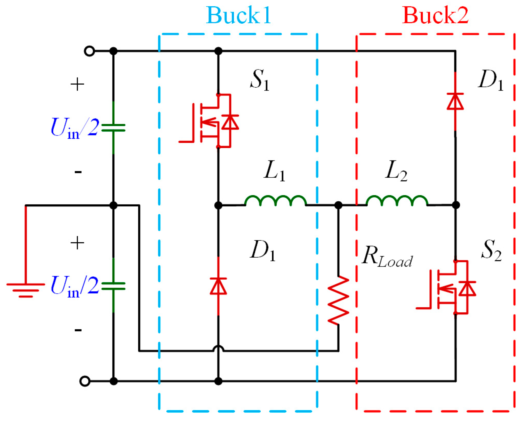
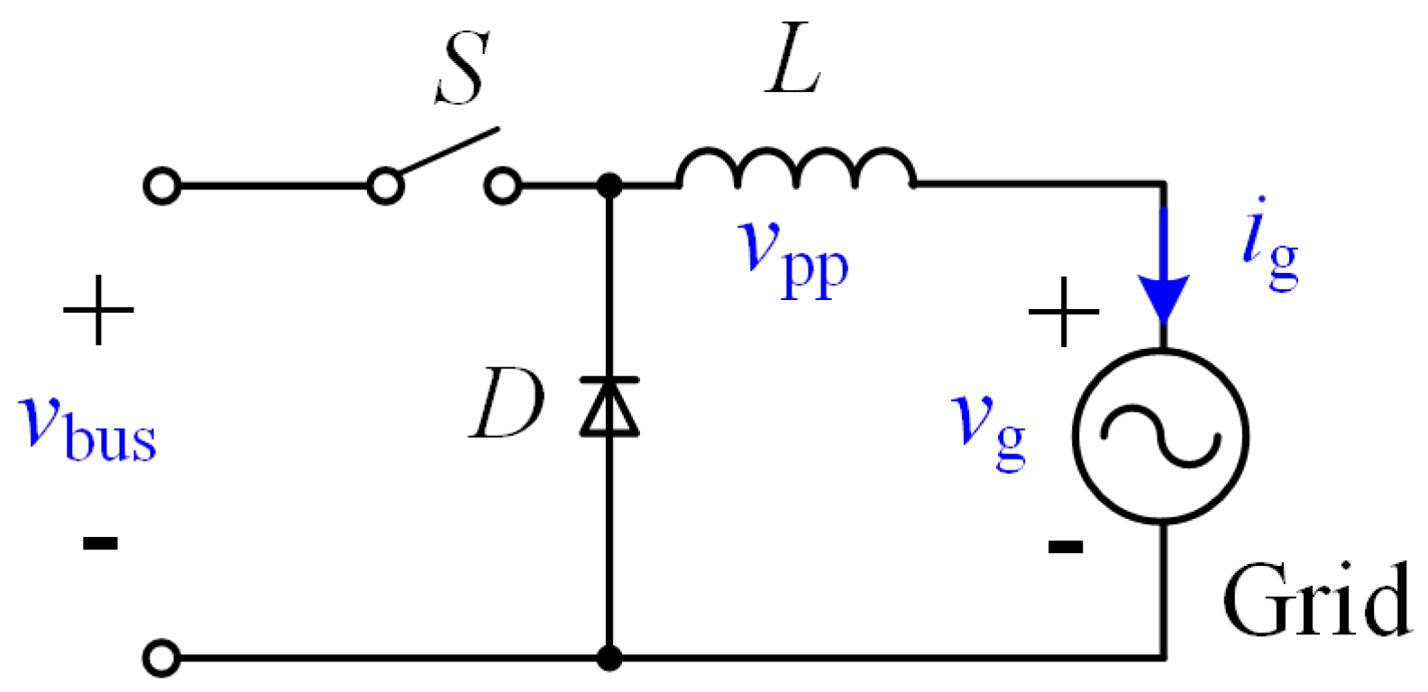
The structure of the dual-buck half-bridge inverter is shown in
Figure 1. The topology is good for its simple structure and ease of control; nevertheless, it still has drawbacks including a low DC voltage utilization ratio and higher voltage stress, which impairs its extensive applications [
6,
7,
8]. In contrast, the full-bridge alternative not only possesses the main advantages of the half-bridge type, but has a high DC voltage utilization ratio and diminished voltage stress [
9,
10].
A family of five-level dual-buck full-bridge inverters with the advantages of multi-level, high reliability, and high efficiency are proposed in [
11]. However, these multi-level inverters often have very complicated topologies which increase the cost of the components and complicate the control method. For small renewable energy applications, cost is one of the most important criteria. A dual-buck inverter with coupled inductors as energy storage branches is described in [
12]. The inverter achieves zero current switching (ZCS) and high efficiency. Moreover, different structures of coupled inductor are discussed in [
13]. By employing coupled inductors, the number of inductors is successfully reduced, but the system efficiency also decreases. However, all of these full-bridge buck type inverters have a switching frequency among 10 kHz to 40 kHz and have a filter inductor volume issue which leads to the decrease of the power density.
Furthermore, the power devices of the inverters mentioned above are all traditional silicon devices, which are not suitable for high speed switching and will reduce the system efficiency. With the development of wide band-gap semiconductor technology, the SiC power devices, which are suitable for high frequency switching, are becoming mature. Contrast analyses have been done between the Si and SiC power devices in different applications [
14,
15,
16,
17]. The results show that the SiC device has lower losses in different implementations and the advantages are more obvious in high frequency applications.
A high frequency single phase dual-buck full-bridge grid-connected inverter for small power renewable energy is proposed. Based on full SiC power switching devices, the operating frequency balloons from the normal 10–50 kHz to the very high 400 kHz, which consequently reduces the filter’s size and the ripple of the grid-connected current. At the same time, limited conversion loss is guaranteed. The design procedure of the proposed inverter is presented and analyzed in detail, which gives a practical design example for a similar type inverter. A three-pole three-zero (3P3Z) compensator is used in the current loop for high frequency compensation. A two-pole two-zero (2P2Z) compensator is used to generate the reference current in order to stabilize the DC bus voltage. Not only is the inner current loop analyzed in detail, which includes the modeling of the equivalent LCL-type inverter and the design of its 3P3Z compensator, but the outer voltage loop is discussed, the model of which is established by energy balance. The control strategy discussed above is actualized by a parallel algorithm on a high performance dual-core MCU. Application details of the proposed algorithm are presented in this paper, including software structure, time-consuming distribution, and the interactive communication method. As a consequence, a 400 kHz high speed control is achieved based on a 1 kW prototype to verify the theoretical analyses.
2. Circuit Configuration and Operation Principles
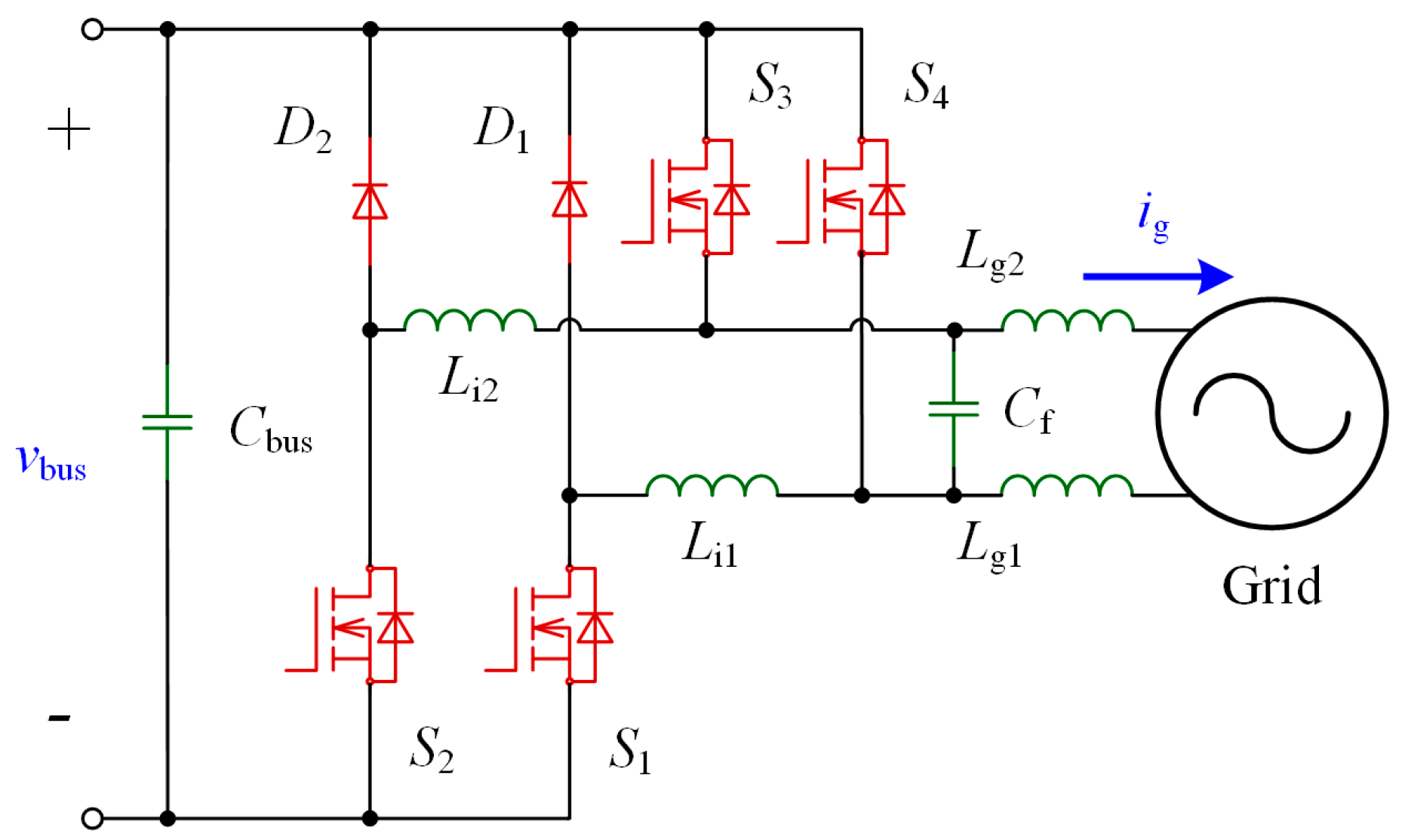
The topology of the dual-buck full-bridge inverter is presented in
Figure 2. The inverter can be regarded as two individual buck converters. One consists of
S1,
S3,
D1, and
Li1, connecting to the DC bus positively. The other is
S2,
S4,
D2, and
Li2, connecting to the DC bus negatively. The output inductors of the buck converters
Li1 and
Li2 constitute a LCL filter with
Cf,
Lg1, and
Lg2. For one AC cycle, both bucks work in their own half cycles separately.
The design features of the inverter are:
- (1)
The structure is simple and no extra power circuit is introduced.
- (2)
Dead time, which is set up to avoid shoot-through, can be ignored because no switch is arrayed in series at the same leg. No dead time makes the implementation of high speed switching more reliable and easy.
- (3)
Comparing to the full bridge topology, only two diodes are added in the dual-buck inverter. The performance of the individual diode is better than the body diode of the switch, which can lower the freewheeling conduction loss.
- (4)
Wide Band Gap (WBG) semiconductor devices are adopted. S1-S4 and D1-D2 are all SiC-based components, which make high speed switching possible and lower the switching losses simultaneously.
- (5)
The high switching frequency shrinks the size and value of the inductors in the converter, making high power density inversion feasible.
2.1. Operation States
To drive the inverter, unipolar modulation has been adopted. The operation principle and modes are analyzed in this section. In order to simplify the analysis procedure, several assumptions are made:
- (1)
All the devices, including switches, diodes, and the grid, are ideal.
- (2)
The current, which goes through Cf, can be negligible compared with the currents of Li1, Li2, Lg1, and Lg2.
From
Figure 3, a full AC cycle can be divided into two separate phases by judging the direction of the output grid current
ig. In Phase 1,
ig is positive. Buck 1, which consists of
S1,
S3, and
D1, works with the LCL filter consisting of
Li1,
Cf,
Lg1, and
Lg2. Similarly, in Phase 2,
ig is negative. Buck 2, which consists of
S2,
S4, and
D2 is working with the LCL filter. In each phase,
S1 or
S2 switches at 400 kHz and
S3 or
S4 switches at AC frequency.
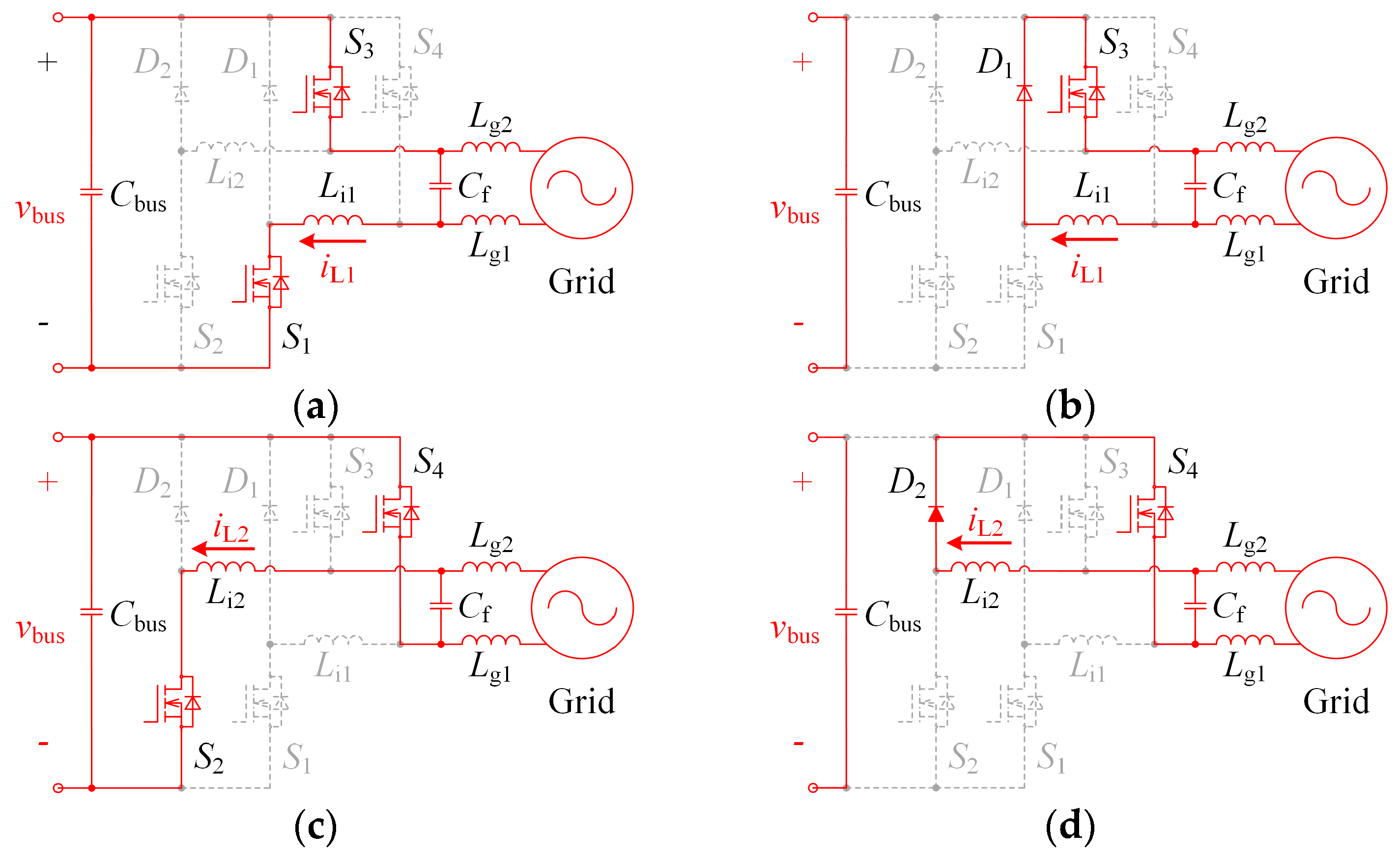
From t0 to t3, assume that ig flows positively. Buck 2 does not work and Buck 1 works alternately to form Mode I to Mode II.
Mode I (
t0-
t1) is shown in
Figure 4a.
S1 and
S3 turn on at
t0.
S2,
S4,
D1, and
D2 are all off. The DC bus,
S1,
S3,
Li1,
Lg1, and
Lg2 are in series to form a loop. The DC Bus charges
Li1,
Lg1, and
Lg2, and the inductor current
iLi1 rises correspondingly.
Mode II (
t1-
t2) is shown in
Figure 4b.
S3 stays turned on at
t1, and
S2 and
S4 are kept off. When
S1 is closed,
D1 turns on. The freewheeling current runs through
D1 instead of the body diode.
Li1,
Lg1, and
Lg2 are discharged and
iL1 decreases linearly.
From t3 to t6, ig is flowing negatively. Buck 1 does not work and Buck 2 alters from Mode III to Mode IV. Mode III and Mode IV are similar to Mode I and Mode II, respectively. Therefore, Mode III and Mode IV will not be discussed in this paper.
2.2. Parameter Design
The LCL-filter has an outstanding performance of attenuating the switching noise, which is better than the L and LC-filters. In order to make the filter function well, the parameters of the filter have to be designed properly [
1,
18].
Section 2.1 shows the operation principles of the inverter, and the two buck converters share
Cf,
Lg1, and
Lg2, which form a LCL filter. For convenience, the equivalent inductors of the LCL filter can be expressed as:
Li =
Li1 =
Li2,
Lg =
Lg1 +
Lg2.
2.2.1. Inverter Side Inductor Li
The main function of
Li is to suppress the current ripple. Neglecting the current through
Cf,
Lg is in series with
Li, and the LCL filter can be simplified as a single inductor
L =
Li +
Lg, as shown in
Figure 5 [
19].
The duty cycle of the equivalent switch is
d, the switching period is
Ts, and the DC bus voltage is
vbus. The relationship between the inductor voltage
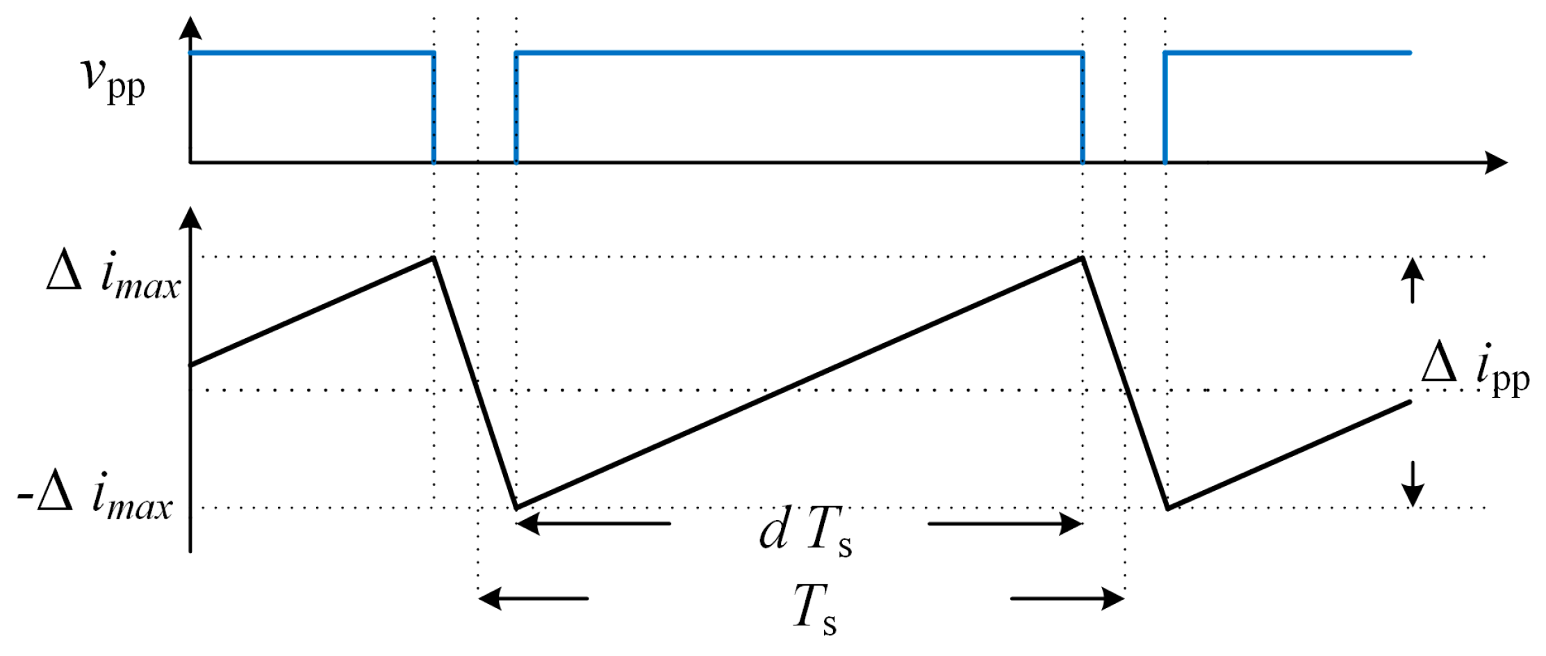
vpp and the peak-to-peak value of the inductor current Δ
ipp is shown in
Figure 6.
In
Figure 6, the inductor voltage is
vpp =
vbus −
vg,
ma is the voltage modulation index,
ωpp represents the peak-to-peak frequency of inductor ripple, and Δ
ipp can be calculated as Equation (1).
From (1), it is noted that the current ripple is not uniform across the sine wave cycle and has a maximum value at sin(
ωt) = 1/2
ma. Accordingly, the maximum current ripple is (2)
The output current ripple should meet the institute of electrical and electronics engineers (IEEE) standard requirement, and thus 5% is chosen as the maximum current ripple. As mentioned before,
L is equal to
Li +
Lg, however, if
Li alone is large enough and satisfies the requirement of the ripple constraint, then
L will meet this requirement as well. The switch frequency is
fsw, and the design equation of
Li is given as:
2.2.2. Filter Capacitor Cf
According to the IEEE-1547/IEEE-519 standard, the maximum reactive power, which is absorbed by the inverter in the rated condition, is 5% of the rated capacity. Hence, the maximum value of the filter capacitor
Cf can be calculated based on the system capacity as Equation (4).
Sn is the rated capacity of the inverter,
Un is the grid voltage, and
ωn is the grid angular frequency.
2.2.3. Grid Side Inductor Lg
The resonant frequency
fres of the inverter LCL filter can be calculated as:
As
Figure 9 shows, the disturbances and noise may be amplified around the resonant frequency. In order to reduce the negative effect of the filter, it is important that the filter has enough attenuation ability at the switching frequency. Thus, the resonant frequency must have a distance from the grid frequency and the distance should be one half of the switching frequency at minimum. By tweaking the
Lg and
Cf values, the resonant frequency can be designed within the desirable range. The component parameters of the proposed inverter will be listed in a later section.
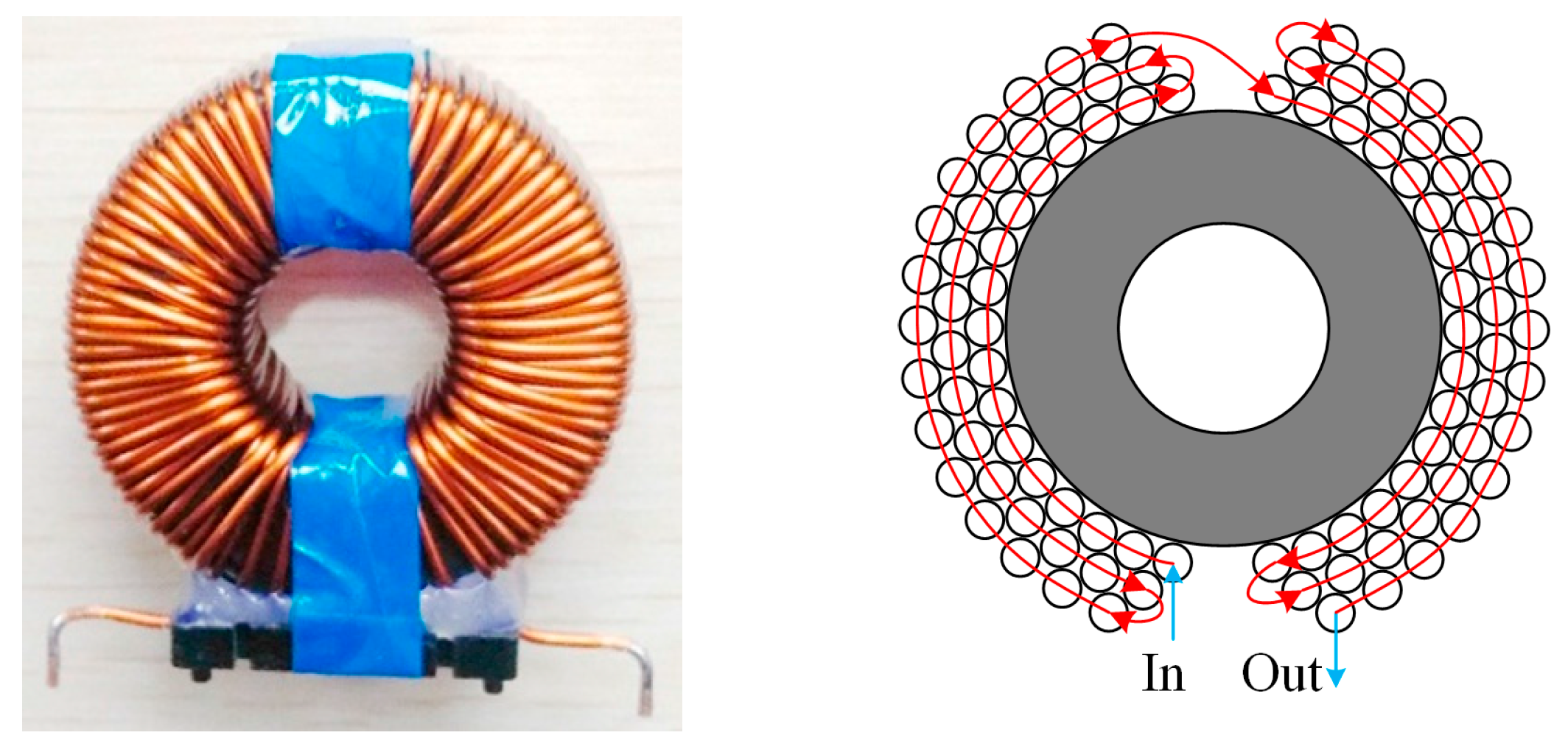
2.2.4. Material and Winding Method of the Inductor
Taking account of the high switching frequency, it is vital to choose the inductor material appropriately in order to reduce the inductor loss. Balancing the cost and performance, sendust is selected as the toroid material. Moreover, the Miller effect may cause oscillation during the switch operation and this problem may get even worse in high speed switching and lead to switching failure. As is shown in
Figure 7, the segment winding method is employed to the halved interlayer capacitance. Hence, the two sections of winding are connected in series with each other and the parasitic capacitance is further reduced.
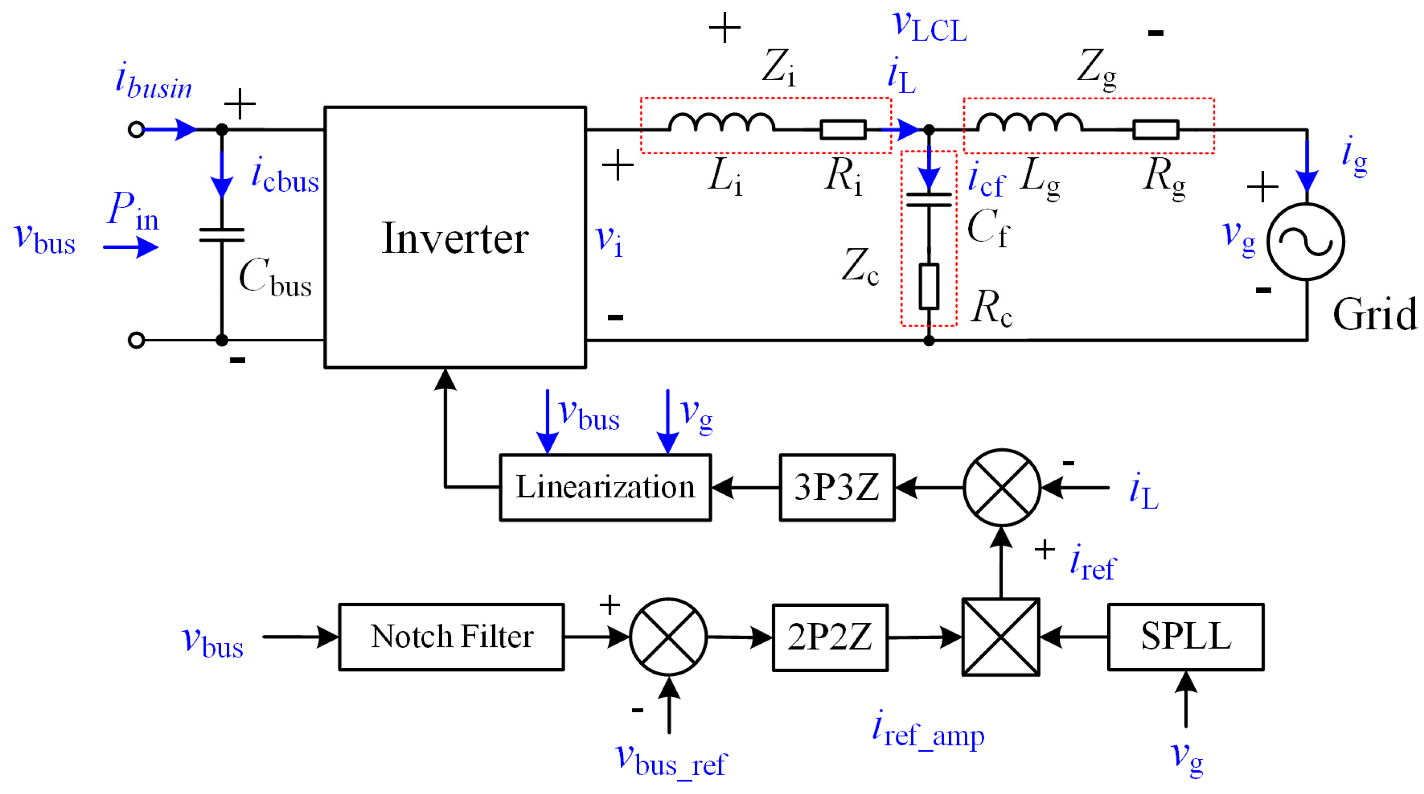
3. Control of the Proposed Inverter
In the renewable energy distributed generation system, it usually has a two-stage structure. The front-stage DC-DC converter adopts the maximum power tracking method to capture energy, while the post-stage inverter transfers the energy into the power grid and stabilizes the DC bus voltage by balancing the input and output power. To actualize these functions, the proposed inverter adopts a current voltage dual-loop. The structure of the control system is shown in
Figure 8.
The bus voltage error is acquired by comparing the measured bus voltage vbus with the bus voltage reference vbus_ref. By injecting the error signal into the 2P2Z compensator, the current reference amplitude iref_amp for the inner current loop is obtained. The SOGI-SPLL measures the grid voltage signal and synchronizes iref_amp with the grid voltage in order to generate the reference current iref. Then, iref is compensated by a 3P3Z compensator. The result goes through a feedback linearization module and becomes the duty cycle which generates the pulse-width modulation (PWM) signal to control the inverter. This method is highly simplified and optimized, which achieves a 400 kHz high speed control.
3.1. Current Loop Compensation
The plant transfer function of the LCL filter for the current control loop can be derived by Kirchhoff's law. The LCL filter is modeled below as (6),
Gig_vi is the plant model for the grid current
ig with regards to the inverter voltage
vi.
The
Zi,
Zg, and
Zc are the impedances of
Li,
Lg, and
Cf respectively. For the proposed inverter, the current feedback senses the
Li current
iL, and the transfer function of
iL with regards to the inverter voltage
vi is
Gp (7)
In the current control mode, the goal of the compensator is to reduce the steady state error to zero. The plant transfer function
Gp and current loop compensator
Gic can be rearranged and bring out the number of integrators.
αp and
αic are the number of integrators in the plant transfer function and compensator, respectively.
Kp and
Gp_r(
s) are the coefficient and plant transfer function after rearranging, respectively, and
Kic and
Gic_r(
s) are the coefficient and compensator transfer function after rearranging, respectively.
The grid voltage
vg(
s) can be approximated to be a ramp signal as Equation (10)
The error
ξ of the grid current
ig, which is caused by the grid voltage
vg, is given below as
Combining with Equations (8–10), Equation (11) can be expressed as
Obviously, to eliminate the state error, the compensator which has a higher number of integrators (αic ≥ 2) must be used.
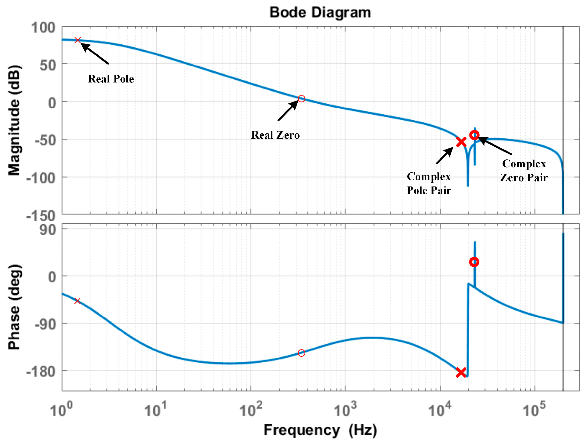
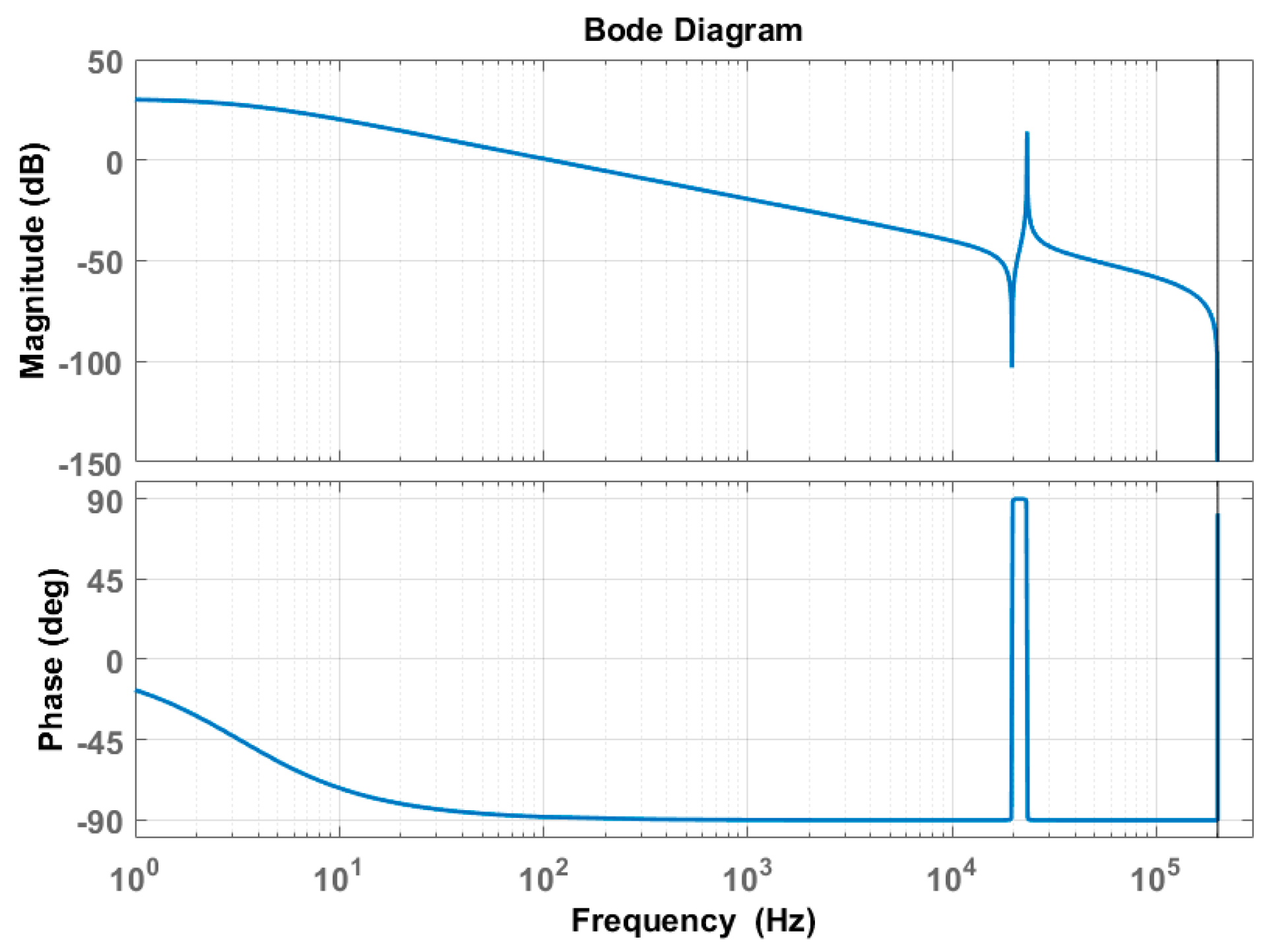
The Bode diagram of the LCL transfer function
Gp(
s) is shown in
Figure 9.
As shown in
Figure 9, the LCL filter presents resonant peaks around the resonant frequency. As a result, the system will be vulnerable and highly sensitive to turbulence and noise which will bring unstable states into the system [
20]. Therefore, a 3P3Z compensator is adopted in order to track the current reference without state error and damps the resonant peak simultaneously.
The compensator is designed in the Matlab SISOtool environment. Graphical tuning is used as the design method. One real pole, one complex pole pair, and one real zero, and one complex zero pair are added in the compensator. The complex zero pair and complex pole pair are placed near the resonance peak. By adjusting the damping factor, the peak can be diminished in order to achieve active damping. Appropriate phase and gain margins can be obtained by tweaking the real pole and real zero positions. The compensator transfer function is transferred in the
z-domain by the Tustin method and is shown in Equation (13).The current control loop Bode diagram is shown in
Figure 10.
After compensation, as shown in
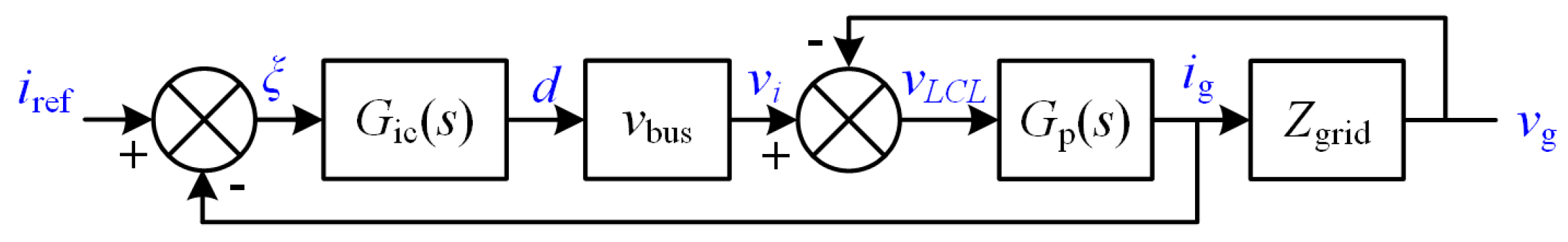
Figure 10, the resonant peak is damped effectively. A gain margin of 38.9 dB and a phase margin of 40.1 degree are achieved. The block diagram of the current control loop, which is based on Equation (11), is shown in
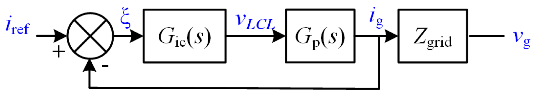
Figure 11.
Where
Gic is the current loop compensator,
d is the duty cycle of the switch,
Zgrid is the grid impedance,
vi =
vbus ×
d,
ig is the grid current, and
iref is the reference current. In order to calculate the duty cycle
d,
Zgrid is needed, but
Zgrid cannot be directly obtained. To solve this contradiction, a feedback linearization method is adopted [
20].
For adopting the method, several assumptions and approximations are made.
- (1)
The change in the inductor current iL has no effect on the grid voltage vg; it is a stiff grid system.
- (2)
The current icf that flows through the filter capacitor Cf is negligible compared to the inductor current iL. Hence, iL = ig.
- (3)
The current controller bandwidth is much higher than the grid frequency, and the feedback path from the grid voltage to the grid controller is broken.
- (4)
The current loop controller is designed such that the current loop gain at the grid frequency is high. As a result, vg can be treated as a DC parameter compared to the dynamics of the inverter inductor current iL; in another word, the current loop crossover frequency is much higher than the grid frequency.
Under these assumption the current controller loop in
Figure 11 can be redrawn as
Figure 12. From
Figure 11,
vLCL can be expressed as Equation (14)
It is clear that the voltage across the output filter
vLCL, and not
vi, has a direct impact on the line current. This is valid when the
vLCL is controlled by a current loop compensator such that the loop gain at grid frequency is high. Hence the compensator must provide the
vLCL. The model of the plant does not change because it takes into account only the small signal behavior. If the compensator provides
vLCL, the duty cycle can be computed as:
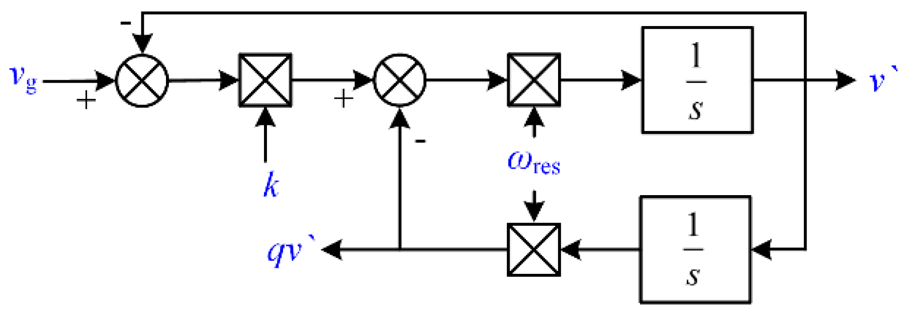
3.2. Second Order Generalized Integrator Software Phase Lock Loop (SOGI-SPLL)
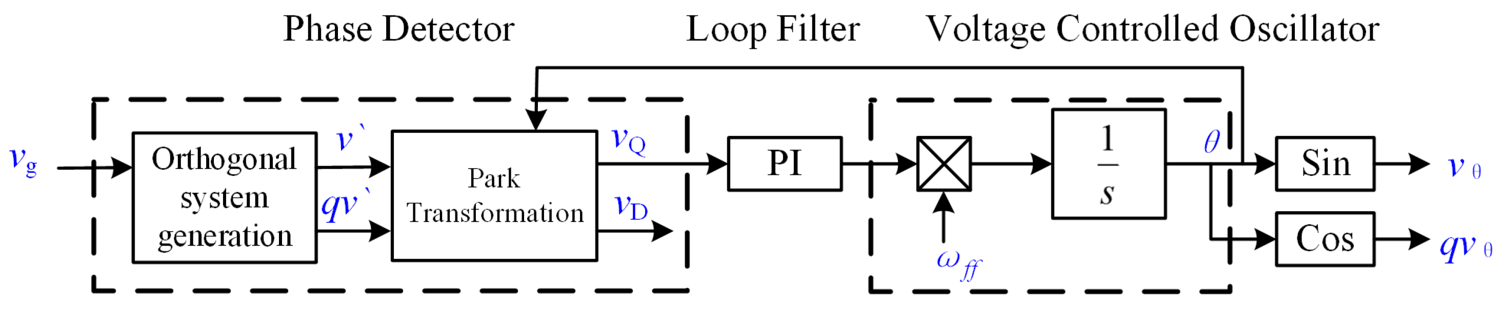
To acquire the phase angle, the SOGI-SPLL method is adopted. The main structure of the PLL is shown in
Figure 13.
Compared with the traditional method, the SOGI method introduces a new type of orthogonal system as shown in
Figure 14.
There are several advantages of this PLL method. First, the generated orthogonal system is filtered without delay due to its resonance at the fundamental frequency. Second, the PLL structure is not affected by the frequency changes. Finally, the simple implementation and low calculation consumption are also important advantages [
21], for the calculation time of the control loop is very limited when the control frequency is high.
As
Figure 13 shows,
vθ is the phase locked signal, which has the same phase angle as the input grid voltage
vg, and
qvθ is the orthogonal signal of
vθ. The reference current
iref can be expressed as Equation (16), where
iref_amp is the active power reference amplitude and i
ref_qamp is the reactive power reference amplitude. Because the inverter only outputs active power,
iref_qamp = 0, and the equation can be simplified as Equation (17). Current
iref_amp is the current reference amplitude, which is generated by the voltage loop.
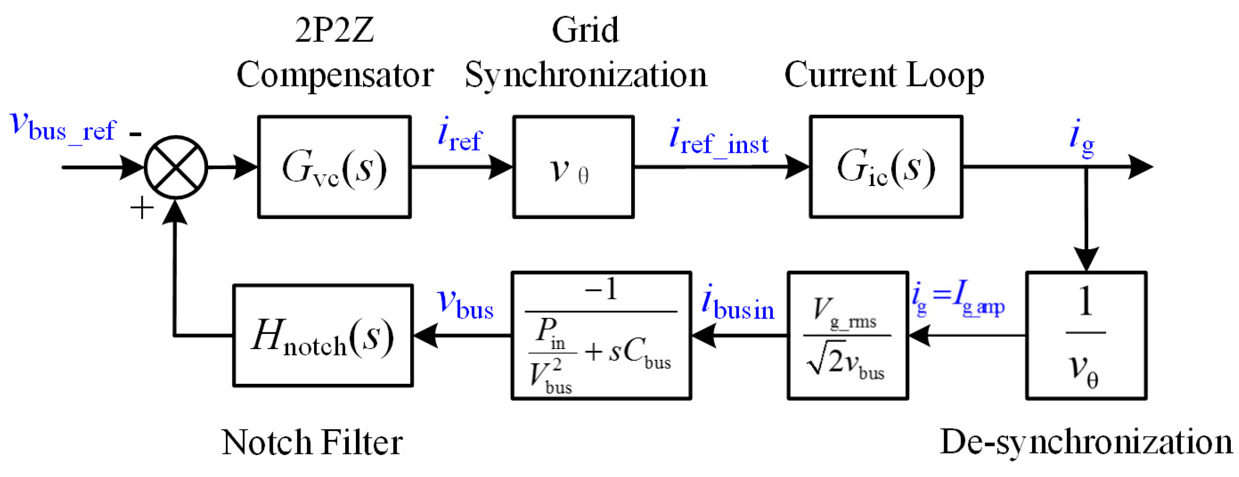
3.3. Bus Voltage Regulation
To stabilize the bus voltage, a 2P2Z compensator is employed to control the voltage loop. According to Kirchhoffs current law (KCL) and Kirchhoffs voltage law (KVL), the relationship between the bus voltage
vbus and bus input current
ibusin can be deduced as
where
Vbus is the nominal bus voltage,
Pin is the inverter input power, and
Cbus is the inverter input capacitor. The grid side voltage
vg and grid current
ig can be represented as
Vg_amp,
Ig_amp are the amplitudes of the current and voltage, respectively.
ωg is the grid angular frequency, and Φ is the phase difference between
vg and
ig. The power balance equation of the inverter can be represented as
Pin is the input power,
Pout is the AC output power,
Pcbus is the power of the capacitor
Cbus, and
PLCL is the power of the LCL filter. In order to simplify the power analysis of the LCL filter, an assumption is made. Considering that the value of the LCL capacitor
Cf is small, the
Cf is ignored. Hence, the inductor currents of the
Li and
Lg are the same, and
Li and
Lg can be considered as a single inductor. The input power, output power, and power of LCL can be expressed as Equations (22)–(24).
Combined with Equations (22)–(24), the power balance equation of the inverter can be represented as
As Equation (25) shows, the bus input current
ibusin can be regarded as a composite variable of a DC component
Ibusin and an AC component
ibusripple. They can be expressed as Equation (26) and Equation (27), respectively.
Vg_rms and Ig_rms are the root meam square (RMS) values of the voltage and current, respectively. The inverter only delivers active power and does not participate in reactive power regulation. Therefore, cos(Φ) is almost 1. The bus voltage contains a double grid frequency ripple. In order to filter out the interference, a notch filter is added in the voltage control loop.
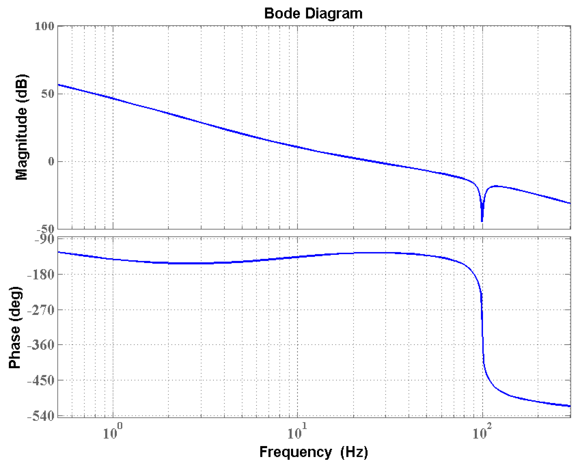
The notch filter can be designed by the FDA tool in the Matlab. The notch frequency is chosen to be 100 Hz and the bandwidth of the filter is 5 Hz for typical applications. The block diagram of the voltage control loop is shown in
Figure 15 and the 2P2Z compensator is shown in Equation (28).
The bode diagram of the whole system is shown in
Figure 16. The input power is 1 kW and cross over frequency is 24.4 Hz. A gain margin of 16.5 dB and a phase margin of 54.4 degrees are achieved. According to the system stability criterion, the gain margin and phase margin are sufficient and the robustness of the system is guaranteed [
22,
23].
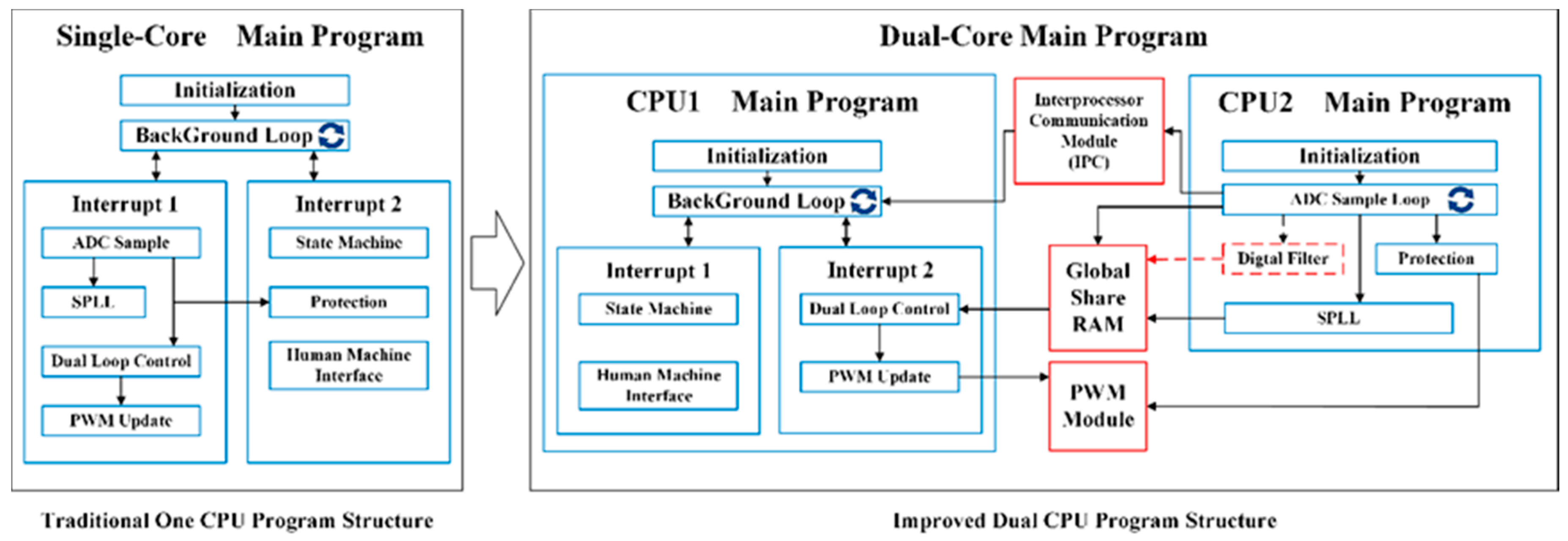
3.4. Dual-Core MCU Algorithm
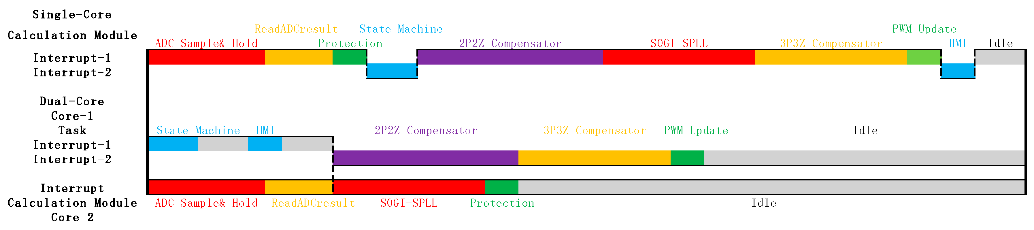
The biggest challenge of the real-time digital control implementation is the calculation speed. Most researchers adopt the analog circuit for loop control when the switching speed is high. Although analog control features innate advantages of high bandwidth, high resolution, and low cost, its control ability is limited to classical control theories. Moreover, the hardware-based structures lack flexibility. By contrast, the digital control is able to perform multiple control loops and advanced algorithms, which make multi-task and multi-function control possible. The software-based compensator can be tuned and expanded easily. Furthermore, the insensitivity to temperature drift and electromagnetic interference (EMI) makes it suitable for high frequency switching control. When the control loop is running at 400 kHz, for a 200 MHz MCU, only 500 CPU clock cycles are available for calculation. The CPU cycle consumption of the main calculation modules are shown in
Table 1 and one CPU cycle is 5 ns.
Obviously, the total time consumption for these main calculation modules almost reaches the MCU process limit of 500 CPU cycles. For this problem, one solution is to manage the calculation with great accuracy and to arrange each step and each interrupt tightly [
24]. The consumption of the computing capability by each module must be measured accurately. This method will greatly increase the difficulty of programming and may cause the program to be unable to modify and expand. Even a small change may overflow the calculation and cause system failure. To overcome this problem, based on a dual-core MCU, a parallel algorithm is adopted. The control program of the inverter can be expressed in
Figure 17.
For a single-core CPU structure, even if the calculation modules are relatively independent, such as the ADC sample and State machine, the calculation has to be executed sequentially. The interrupt mechanism only affects the sequence of execution but not the total calculation time. Unlike the one-core CPU interrupt strategy, the calculation modules of the program, which are not directly combined, can be executed in parallel at the same time by dual CPU cores. Ideally, the calculation time can be reduced by half. The dual CPU structure is shown in
Figure 17. In order to simplify the communication between different CPUs, the modules, which are relatively independent, are distributed in the same CPU. For example, the ADC sample, SOGI-SPLL, and Protection modules are assigned to CPU2. As a result, the main data flow is almost in one direction towards CPU1 because those function modules only need to send the data to CPU1. The only communication which is needed is the acknowledgement from CPU2 to CPU1. The acknowledgement is the signal which CPU2 completes the ADC sampling procedure and finishes writing the results to the global share RAM. CPU1 receives the signal, reads the ADC results from the global share RAM, and begins the calculation. The acknowledgement mechanism is implemented by the interprocessor communication module (IPC), which is designed to communicate between the two CPUs. The ADC results are transmitted through the global share RAM, which is suitable for data transfer.
As
Figure 18 shows, the calculation modules are rearranged for both CPU cores, and the calculation quantity of CPU1 is greatly reduced. As a result, both CPUs have unused computing margins for further applications, such as digital filters. For the powerful calculation ability and flexible expansion capability, the dual-core MCU system is well suited for a high switching frequency inverter.
4. Experimental Results
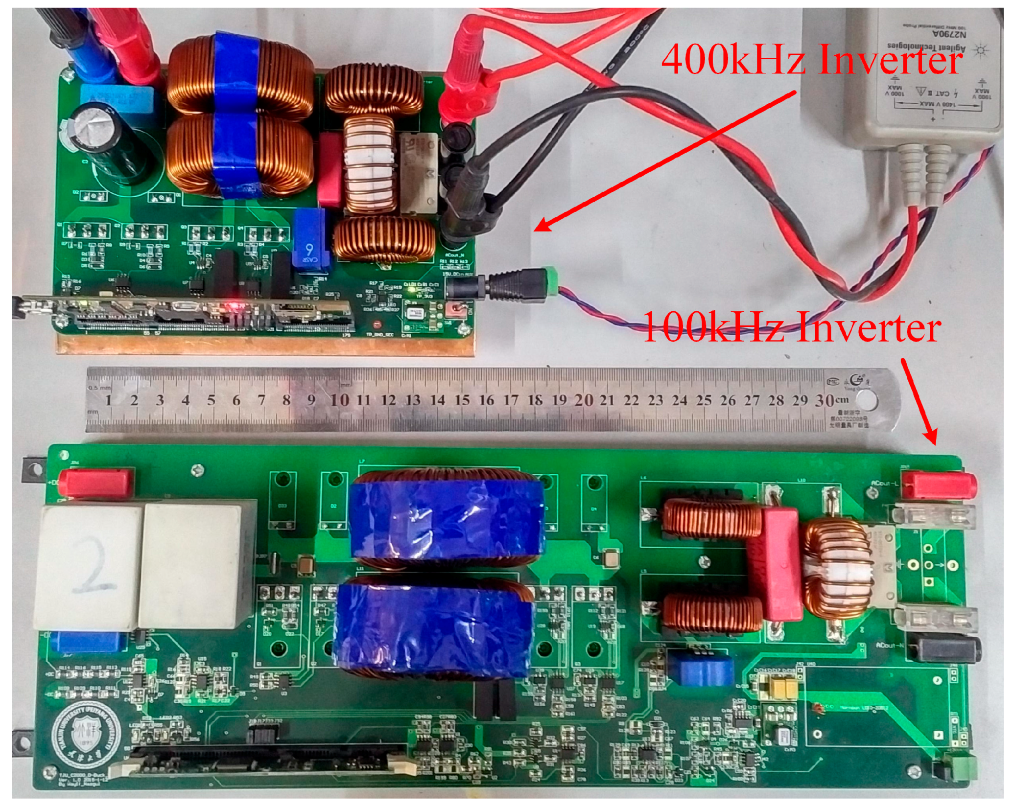
To verify the validity of the theoretical analyses, a 1 kW prototype was built in the laboratory, shown in
Figure 19. The 400 kHz inverter is about half the size of the previous 100 kHz prototype. The power density and portability are significantly improved. The parameters of the components are shown in
Table 2. The control platform is a TMS320F28377D from Texas Instruments. It is a high performance dual-core MCU running at 200 MHz.
Figure 20 shows the output current
ig at 100 W. The output current
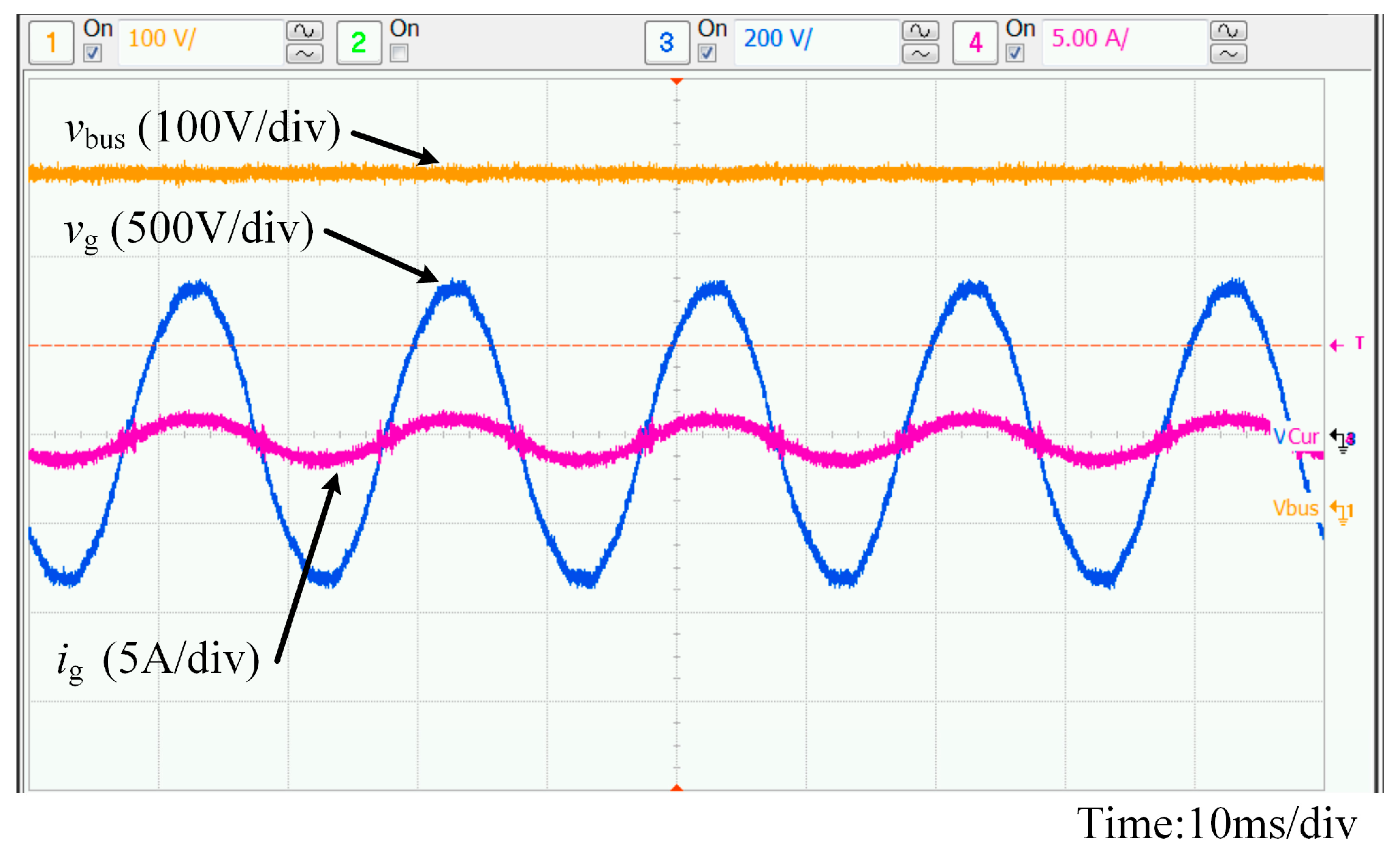
ig can track the grid voltage very well when the power output is low. The power factor is 0.99 and the total harmonic distortion THD is 4.8%. The bus voltage is stabilized at 400 V and the ripple is within ±4 V.
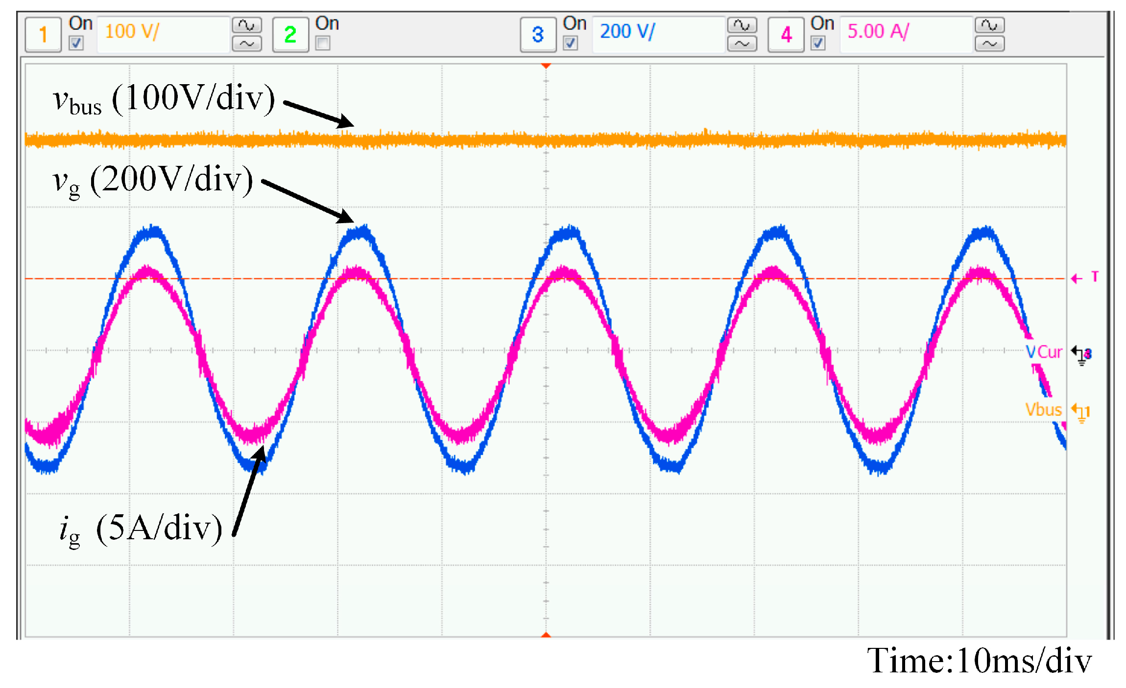
Figure 21 shows the output power at 1 kW. The RMS value of
ig is 4.5 A. Along with the increase of the output power, the waveform of the
ig increases significantly. The power factor is 0.99 and THD is down to 1.8%. The efficiency of the inverter is 96.1% at this moment.
Also from
Figure 20 and
Figure 21, it indicates that the proposed inverter can obtain power factors near unity for the output current, constrained THDs, and relatively high efficiencies among the full load range at 400 kHz. For the next-stage work, the efficiency can be further improved through adding resonant snubbers, which may help the inverter to achieve soft-switching characteristics.
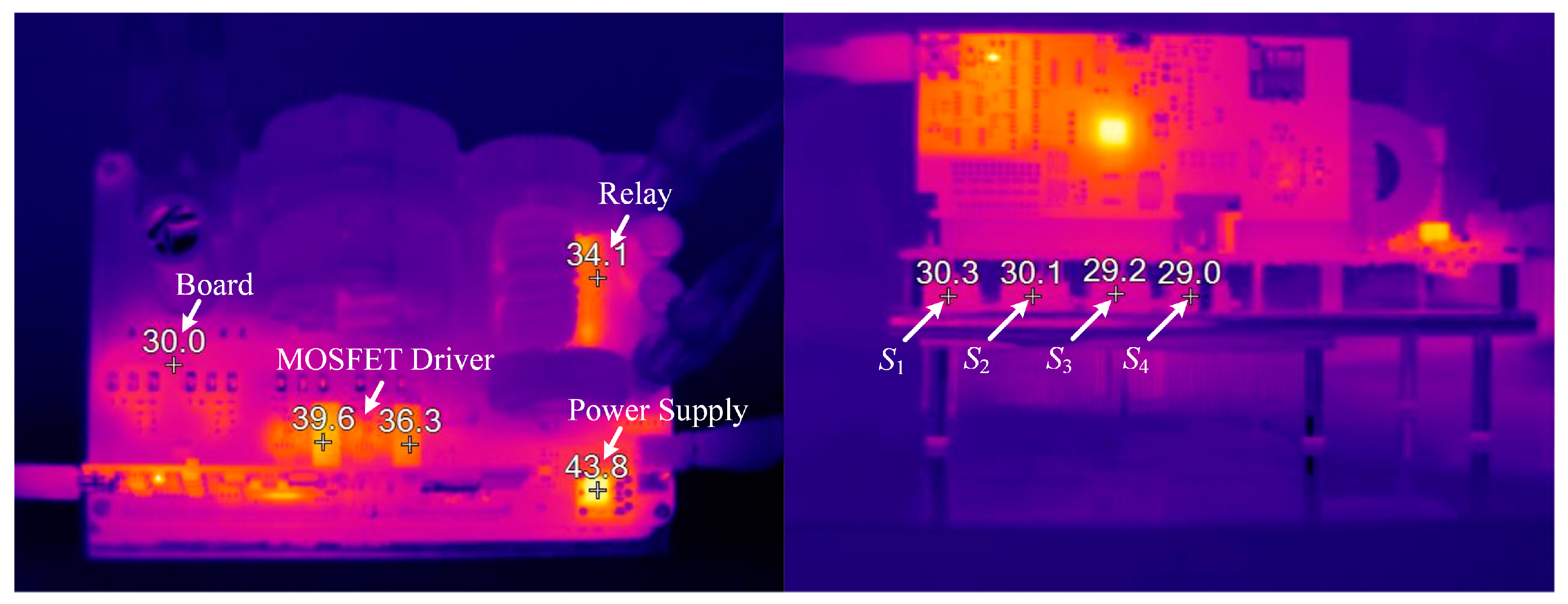
Figure 22 shows a thermal image of the inverter at 1 kW. The temperatures of the switches
S1-
S4 are around 30 centigrade and that of the metal-oxide-semiconductor field-effect transistor (MOSFET) driver is under 40 centigrade. The highest hotspot is the power supply at 43.8 centigrade. Due to the high efficiency and thermal design, the component temperature is in the controllable range, which leaves margins for further higher power levels.
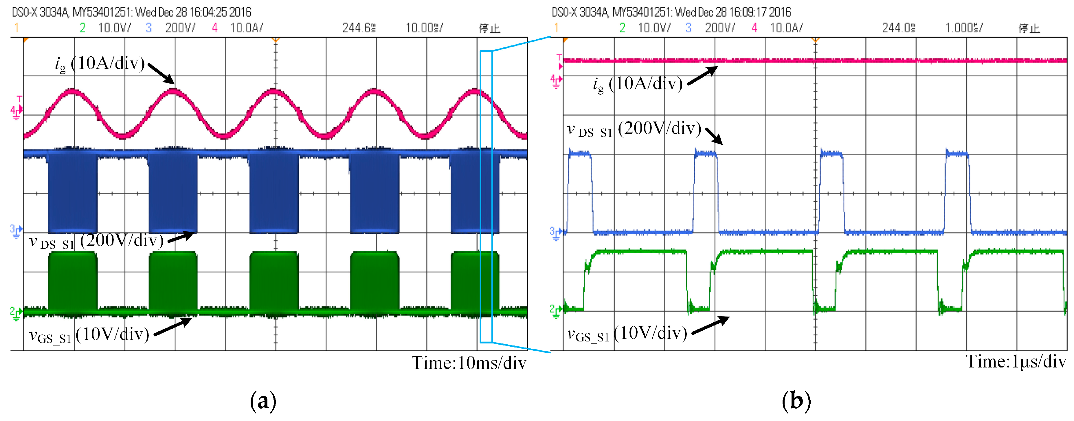
Figure 23a shows the waveforms of the switch and grid current at 1 kW.
Figure 23b is the partial enlarged waveform.
ig is the grid current of the inverter.
vDS is the drain-to-source voltage of the switch
S1.
vGS is the drive signal of
S1. As the waveform shows, when
ig is above zero,
S1 is switched at the high frequency of 400 kHz and thus
ig in phase with
vDS_S1. The voltage stress of
S1 is 400 V. Then when
ig flows negatively, both switches
S1 and
S3 will not function, and instead,
S2 and
S4 will continue to operate.
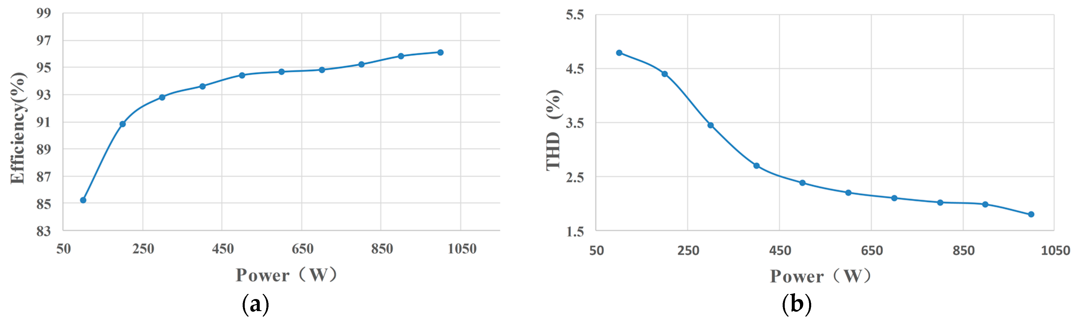
Finally, the relationships between efficiency and THD versus the output power are shown in
Figure 24a,b, respectively. The efficiency increases from 85.2% to 96.1% when the output power grows from 100 W to 1000 W. The efficiency reaches the maximum efficiency of 96.1% at the rated condition. The THD is 1.8% at the rated condition. Thus, in small renewable energy applications [
25,
26,
27], the proposed inverter can achieve outstanding performances, including a relatively high conversion efficiency, high power factor, and low THD.


