Article

Characterization of the Diamond Wire Sawing Process for Monocrystalline Silicon by Raman Spectroscopy and SIREX Polarimetry

1
Fraunhofer Technology Center for Semiconductor Materials (THM), Am St.-Niclas-Schacht 13, D-09599 Freiberg, Germany
2
PVA Metrology & Plasma Solutions GmbH, Am Naßtal 6/8, D-07751 Jena-Maua, Germany
*
Author to whom correspondence should be addressed.
Energies 2017, 10(4), 414; https://doi.org/10.3390/en10040414
Submission received: 30 November 2016 / Revised: 16 March 2017 / Accepted: 18 March 2017 / Published: 23 March 2017
(This article belongs to the Special Issue Crystalline Silicon Solar Cells: Fundamentals and Technologies)

Abstract

:
A detailed approach to evaluate the sub-surface damage of diamond wire-sawn monocrystalline silicon wafers relating to the sawing process is presented. Residual stresses, the presence of amorphous silicon and microcracks are considered and related to diamond wire velocity and cutting ability. In particular, the degree of amorphization of the wafer surface is analyzed, as it may affect the etching performance (texturing) during solar cell manufacture. Raman spectroscopy and Scanning Infrared Stress Explorer (SIREX) measurements are used independently as non-destructive, contactless optical characterization methods to provide stress imaging with high spatial resolution. Raman mappings show that amorphous silicon layers can occur inhomogeneously across the surface of diamond wire-sawn wafers. The Raman and SIREX results reveal a connection between a higher fraction of the amorphous phase, a more inhomogeneous stress distribution and a lower peak maximum of the stress difference on wafers, depending on both the wire wear and the wire velocity. SIREX line scans of the in-plane difference of the principal stress components ∆σ taken across the sawing grooves show significant differences in magnitude and periodicity. Furthermore, the results are compared with the microcrack depth from the same investigation areas. The possibility to optimize the diamond wire sawing processes by analyzing the sub-surface stress of the wafers is offered by complementary use of both Raman and SIREX measurements.

1. Introduction

The diamond wire sawing technique induces a damage structure on the silicon wafer surface as the fixed diamond particles on the wire scratch over the silicon surface [1,2]. This scratching produces a characteristic damage pattern of parallel and shallow grooves with chipped and polished areas. The surface quality of diamond-sawn wafers is inhomogeneously rough compared to wafers produced by a slurry-based method. Depending on the sawing conditions, different degrees of wafer damage can occur. The properties of the silicon surface structure that are of interest include the topography and changes to the lattice structure due to phase transformations and mechanical stresses. Mechanical stresses are reduced by the formation of microcracks and may as well lead to deformed sub-surface regions. The degree of the amorphization of the wafer surface could potentially affect the etching performance (texturing) during solar cell production and needs to be analyzed.
Two independent non-destructive, contactless stress imaging methods, which have recently been shown to be beneficial [3], were used to investigate the sub-surface damage herein, Raman spectroscopy and Scanning Infrared Stress Explorer (SIREX). The high spatial resolution of these methods can reveal features of the surface damage that are not displayed by standard investigations, providing more insight into the sawing process. A statistical analysis of the maps reveals characteristics that can be correlated with key parameters of the sawing process. The analyses were performed on monocrystalline silicon wafers sawn with different wire velocities. Furthermore, wafers from brick positions cut by fresh and by used wire were investigated in order to reveal the effect of wire wear on the degree of the sub-surface damage.
In this work, Raman spectroscopy mapping has been applied to locally detect the total residual material stress σ and the amorphous to crystalline silicon phase ratio r. Additionally, different wafers were scanned using the SIREX photo-elastic microscope [4]. SIREX is a reflection-based plane polarimetry that measures the depolarization of an initially linear polarized laser beam after penetrating the wafer. A complete SIREX analysis delivers a map of the difference in the in-plane principal stress components, ∆σ.
Until now, the analysis of cracks on polished and etched bevel-cut samples using confocal laser scanning microscopy (CLSM) has been the standard method to characterize the sub-surface damage of wire sawn wafer surfaces. Therefore, the Raman and SIREX results have been correlated with the results of these microcrack depth investigations.

2. Materials and Methods

2.1. Sample Description

Monocrystalline silicon wafers (PV-grade Cz-silicon, p-type) sawn with wire velocities of 10 m/s, 15 m/s and 20 m/s under a constant feeding rate were used (see Table 1 for the main process parameters). The wire was not dressed before, thus a significant wire wear is expected. After sawing the wafers were treated with a standard alkaline cleaning medium, by which particles and chemical contaminations are removed from the wafer surface. The wafer cleaning process consists of several cleaning steps using a surfactant with sodium hydroxide (pH value is about 12) and rinsing with deionized water. Each step is carried out under thermal ultrasonic environment with different frequencies (up to 70 °C, 20–30 min, 25–120 kHz).
The analyzed monocrystalline silicon wafers (156 × 156 × 0.22 mm3) with a {001} surface orientation were taken from the wire entry side along a brick, where fresh wire is supplied (low wafer numbers of the brick), and from the used wire side (high wafer numbers). Detailed investigations were conducted at five positions on each wafer: near the wire web edge (“cut-in edge”), in middle of the wafer (“center”), near the glued side (“glue edge”) as well as at the center-left (“left”) and center-right (“right”) of the wafer edge; see the green areas shown in Figure 1.

2.2. Measurement Procedure

2.2.1. Raman Spectroscopy

Using Raman spectroscopy, the distribution of absolute in-plane stresses σR = (σ1 + σ2)/2 (in the polarization direction of the incident beam) [3,4,5,6] and phase transformations can be investigated in detail by analyzing the crystalline silicon (c-Si) peak position and peak width. The Raman spectrum of unstrained c-Si exhibits a sharp and totally symmetrical phonon band peak around the wave number 521 cm−1 [6]. The shifts of the peak position reveal tensile and compressive stresses, which appear as negative or positive peak shifts, respectively. The peak shifts were calibrated to a stress value according to ref. [7]: a Raman shift of ±3.2 cm−1 corresponds to ±1 GPa stress.
Raman spectroscopy can also be applied to determine the Raman intensity ratio r of the amorphous to crystalline silicon phase: r = Ia-Si/Ic-Si [8,9]. The main peaks of amorphous silicon (a-Si) are located at 470 cm−1 and 150 cm−1. The fractions of both a-Si and c-Si are obtained from the integrations of the total Raman intensities, Ia-Si and Ic-Si, of the related Raman peaks. The larger the value of r, the greater is the amorphous silicon fraction, and therefore the thicker is the amorphous layer. The a-Si/c-Si ratio r allows for conclusions about the distribution and the thickness of the amorphous silicon layer on a wafer surface. The a-Si fraction on wafer surfaces can vary significantly, as previously shown [9]. The experimental procedure for the evaluation of the amorphous silicon fraction and layer thickness has been explained in our previous contribution [9].
For all Raman mappings, an excitation laser wavelength of 532 nm and a laser power of 1.2 mW incident on the wafer surface were used. At this wavelength, the laser light penetrates approximately 800 nm into the silicon material. Raman mapping with a high spatial resolution of 5 µm is very time-consuming, e.g., area of 320 × 200 µm2 is scanned within 20 h. Therefore it is impossible to map the entire wafer surface. Thus, five restricted areas are measured on each wafer.

2.2.2. SIREX Polarimetry

The photo-elastic SIREX microscope is a reflection-based plane polarimeter especially developed for the high-resolution visualization of the stress state in silicon-based electronic and mechanic devices. SIREX measures the depolarization of an initially linearly polarized infrared laser beam after reflection at the front and the back side of the wafer. In the case of rough wafer surfaces, which are measured here, the surface itself can also contribute to the depolarization.
In ref. [3] experimental investigations on a single scratch have been carried out to analyze the depolarization effect due to the surface topography. Confocal laser scanning microscopy images with a high spatial resolution were used to determine the orientation of local surface elements. With a ray tracing program the optical reflection onto the detector and the local depolarization have been calculated for each surface element based on the Fresnel equations. Due to the small aperture of the detector only surface elements, which are inclined perpendicular to the incoming beam by less than 1° will reflect light onto the detector. The quantitative comparison of the results with the measured SIREX topogram at the same positions has shown that the depolarization effect of the surface topography is about one order of magnitude smaller than the measured values. It has therefore been concluded that the main effect is due to stresses inside of the wafer and that SIREX measurements can be performed on wafers with rough surfaces.
In the SIREX method a procedure is applied where the initial polarization is rotated around the beam direction. This allows determining the difference of the in-plane principal stress components ∆σ = σ1σ2 (see details of the technique in [4]). One can estimate from the results in [3] that there is a lower detection limit of stress differences of about 0.05 MPa. Since the bulk of the wafers, which are investigated here, is stress-free the subsequent analysis of the reflected depolarized laser light can be based on the assumption that the sub-surface stresses generate the in-plane anisotropy of the refractive index, known as optical birefringence.

2.2.3. Confocal Laser Scanning Microscopy

The depth of the microcracks resulting from the abrasive process during diamond-plated wire sawing is determined using a confocal laser scanning microscope (CLSM). Bevel-cut samples of 1° inclination are prepared by mechanical polishing perpendicular to the saw marks and treated for 30 s with Secco etch (hydrofluoric acid and potassium dichromate solution at a ratio of 2 to 1, [10]). On the polished and etched beveled part of the sample, the damage structure with microcracks becomes visible on the surface. With increasing depth, the microcracks gradually vanish. To determine the deepest microcracks in the sample, the surface height profiles parallel to the sawing marks are measured, and the difference is determined between the height of the original sample surface and the one at which the last microcrack is visible [9].

3. Experimental Results and Discussion

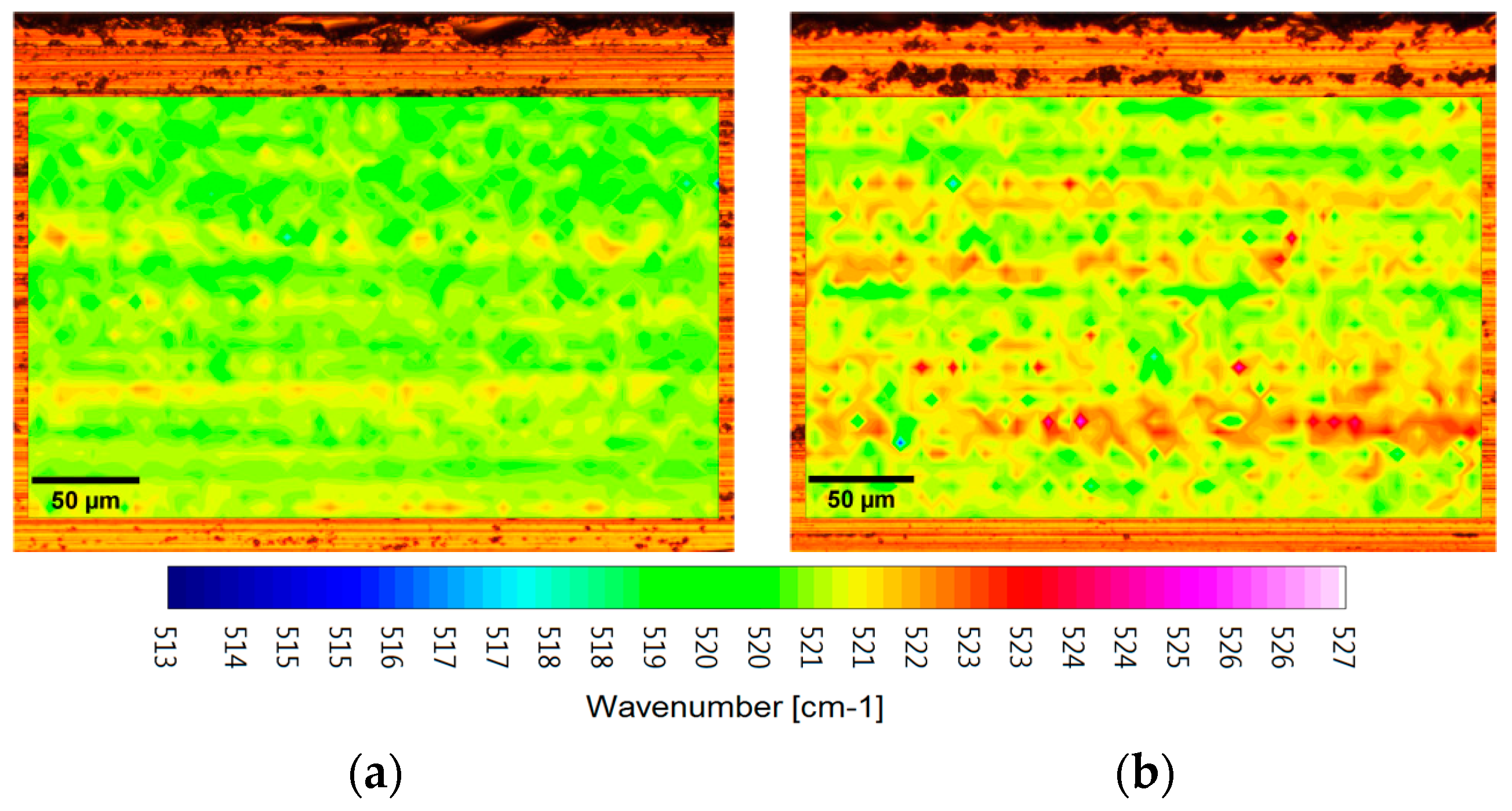
3.1. Investigation of Surface Amorphization and Material Stresses with Raman

The amorphous silicon phase fraction r and the absolute stress (σR) distribution on the wafer surfaces, depending on the wire velocity and the wire wear, were detected by Raman spectroscopy (Bruker Optik GmbH, Leipzig, Germany).
The investigations were performed on three fresh (wafer number 006) and three used wire wafers (wafer number 240), sawn with wire velocities of 10 m/s, 15 m/s and 20 m/s. The wafer surface was measured at five different positions by Raman spectroscopy. Each Raman area was evaluated with regard to the amorphous silicon fraction.
Figure 2a,b depict the mean value of the Raman intensity ratio r of the amorphous to crystalline silicon phase for the measured areas on the fresh and used wire wafers. The amorphous silicon layers are inhomogeneously distributed on the wafer surface. The results for the wafers of the fresh wire side show no dependence of amorphization of the wafer position (Figure 2a). By contrast, there is likely an increasing trend from the position cut-in edge to glue edge on the wafers of the used wire side, see Figure 2b. This would imply that the degree of amorphization is correlated with the wire wear, since the sawing performance with used wire, where the diamond edges are worn, is less good. That is reflected in a higher amorphization of the silicon surface. Since the worn diamonds have a lower cutting ability, more energy may be used for the amorphization of silicon. The highest amorphous silicon fraction is found near the gluing edge, where the ductile material removal process is the dominating effect. This results in a smoother surface with less chipping pits in the surface. Enhanced amorphization is also present on the left and right wafer edges compared to the wafer center. By using fresh wires, where the diamond edges are sharp, a brittle material removal is dominated and a surface with a lot of chipping is present. Regarding the wire velocity, the lowest fraction of amorphous silicon phase is found for the sawn wafer at 10 m/s, and the highest mean value is found for the wafer sawn at 15 m/s.
Table 2 presents an overview of the evaluated amorphous to crystalline silicon ratios r from the Raman data, and the resulting depth of the amorphous layers for fresh and used wire wafers (a theoretical relationship between r and the depth of the amorphous layer is presented by Yan et al. [8]). A total area of 1.6 × 1.1 mm2, made up of five distributed areas, was measured on each wafer. The results show significantly higher r-values for the wafers from the used wire side. Therefore, a clear relationship between a higher fraction of the amorphous phase on the wafer surfaces and the wire wear can be identified. In addition, the amount of amorphous fraction on the wafer surface depends on the wire velocity [9]. The lowest r-values are determined for the slowly sawn wafer (10 m/s).
In addition, the topographical Raman measurements were analyzed with respect to the stress-induced wave number shift of the crystalline silicon peak. Figure 3 presents an example of high-resolution Raman maps showing the crystalline peak shift acquired from the fastest sawn wafer (20 m/s) for both the fresh and used wire side. The typical sawing-induced stripe pattern is observed on all wafers. Furthermore, the c-Si wave number maps depict a more homogeneous stress distribution for the fresh wire wafers. Essentially, the measurements of the sawn wafers from the used wire side indicate locally intensified compressive stresses (positive Raman shift) parallel to the sawing grooves of up to 1.8 GPa. It follows that the stress distribution correlates with the wire wear.
For the measured wafer position near the glue edge, the normalized relative frequencies of the Raman c-Si wave numbers are exemplarily plotted in Figure 4. The frequency distributions show a significantly higher half width for the wafers from the used wire side (marked by blank symbols). This difference is directly associated with the c-Si wave number spread, which can be interpreted as a more inhomogeneous stress distribution. The maximum of the frequency curve of the used wafer with 15 m/s is shifted to higher wave numbers. Also wafer used-20 m/s show a peak shifting in the same direction, albeit somewhat less than used-15 m/s. Generally, the used wafer with 15 m/s shows the highest local compressive stress on the silicon surface compared to the other investigated wafers.
For a detailed analysis in dependence on the measured wafer position, the topographical Raman data were statistically evaluated. Figure 5a gives an overview of all mean values of the c-Si wave number peak positions and Figure 5b depicts the Raman shifts with respect to the c-Si peak at 521 cm−1 for the fresh and used wire wafers at the five mapping spots. Both wafers sawn with the highest wire velocity (20 m/s) show the same likely trend. Generally, except for wafer 10 m/s, the largest mean values are found in the center position of the wafer. Thus, the wafer center seems to be more compressively stressed than the areas at the wafer edges. This might be explained by the wire wear, which is in an equilibrium state at this cutting depth, since the wire web is completely exchanged at this position due to the addition of fresh wire in each forward-backward-cycle. This might affect the removal mechanism as well, leading to different stresses. Except for wafer 15 m/s fresh, the wave number values for the upper position close to the gluing edge, where the wire is worn due to the sawing process, are higher than for the position near the cut-in edge. Fresh sawing wires have sharper diamond edges and therefore better cutting performance than used ones. Therefore, the silicon material is expected to be more stressed in the wafer region at the cut-in edge.

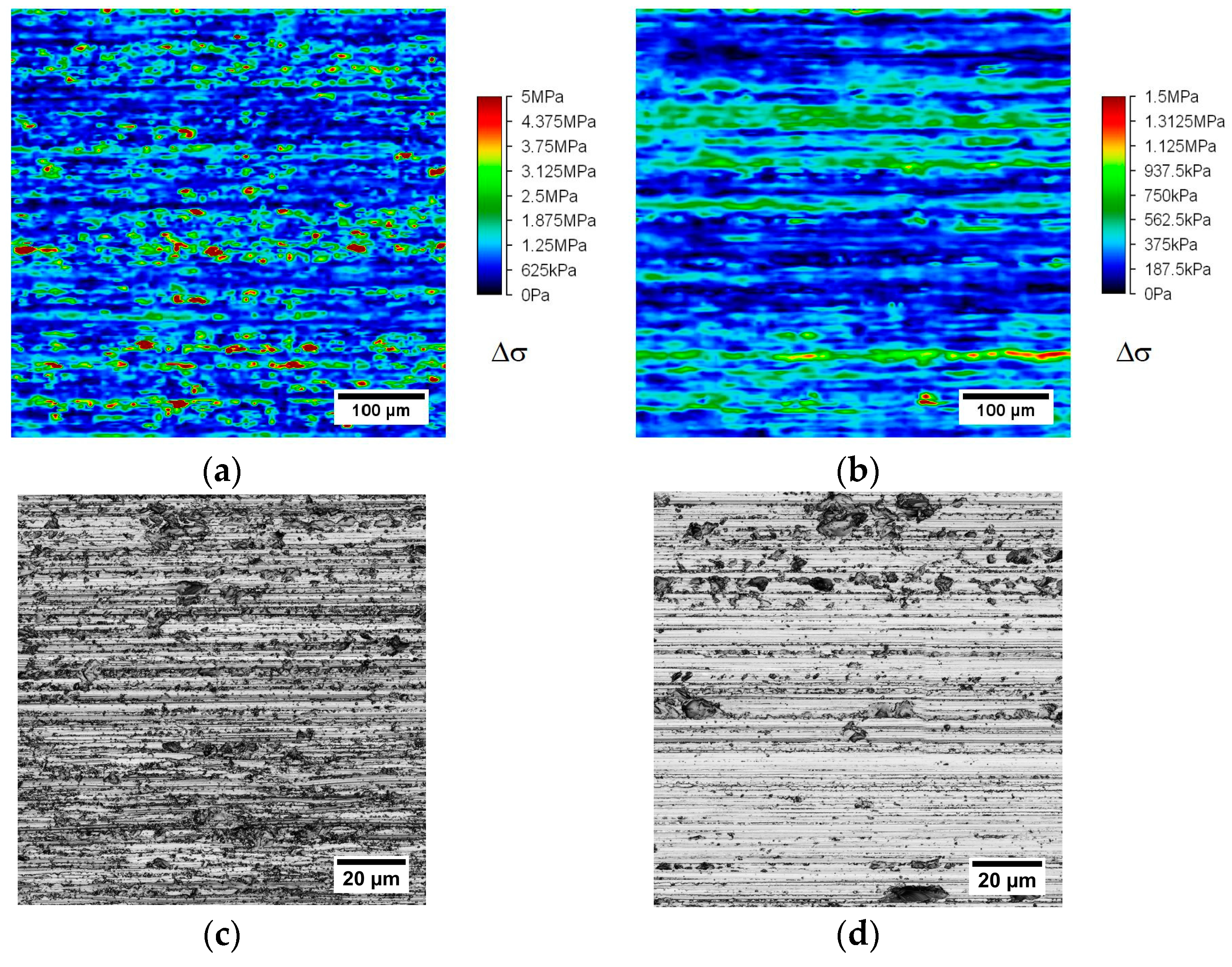
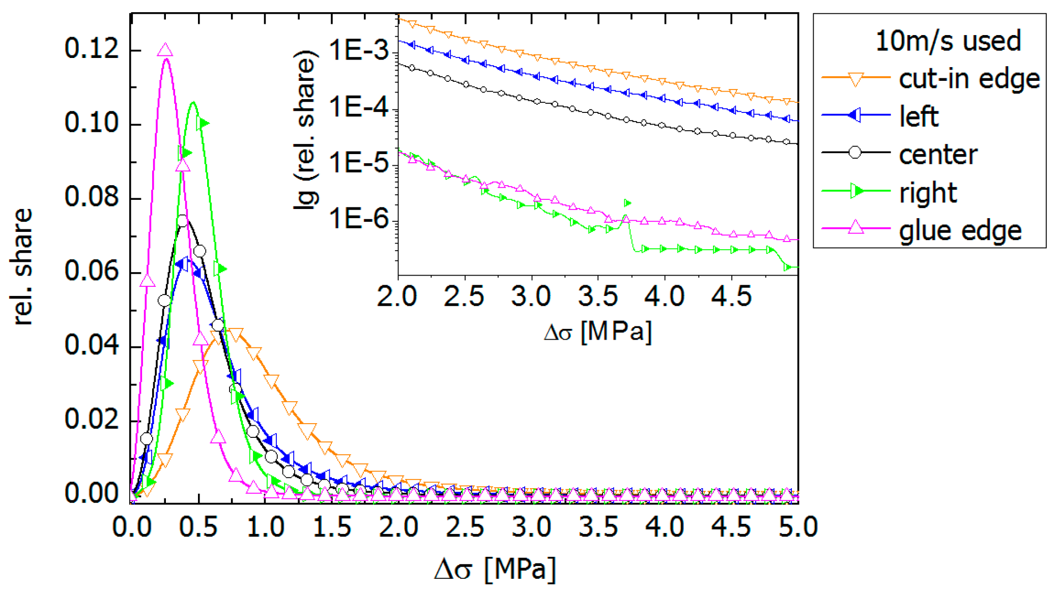
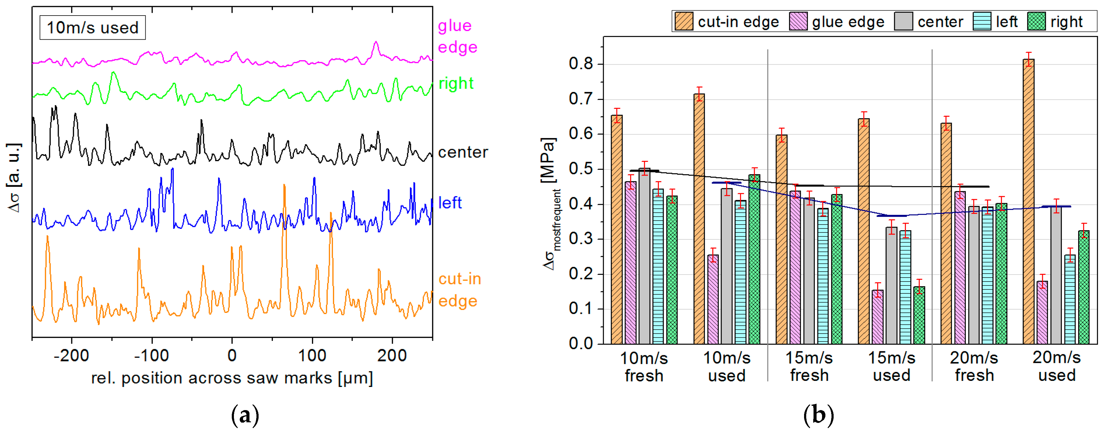
3.2. Characterization of Sub-Surface Stresses with SIREX

A detailed approach to investigate the degree of sub-surface stress using the SIREX photo-elastic microscope (PVA TePla, Jena-Maua, Germany) was employed here. The values of the stress differences ∆σ can be correlated to the wire velocity and wire wear.
The scanning infrared reflection topography measurements by SIREX reveal the lateral distribution of the in-plane shear stress as a measure of the damage across a wafer, as demonstrated by the comparison of maps taken at different positions on a wafer. Figure 6a,b show two maps of the calculated difference ∆σ of the in-plane principal stress components σ1σ2 at the lower cut-in edge and the upper gluing edge of a wafer. The maps clearly reproduce the structure of the sawing grooves. The maximal measured stress difference is significantly higher near the cut-in edge position than at the gluing edge.
The topogram near the cut-in edge (Figure 6a) is also characterized by a higher density of local high stress regions (“red spots”). As it has been discussed in Section 2.2.2 the surface topography itself does not contribute to the evaluation of the stresses, but certain features may correlate with higher stresses below the surface. Corresponding confocal laser scanning microscopy images (see Figure 6c,d) of the same areas show that the visible characteristic shallow pits, where material is chipped away, do not directly correlate with the red spots. In fact, one would actually assume that by chipping material away previous local stresses have been removed here. A further analysis of the sub-surface damage at the high stress positions, which is responsible here, has not been carried out so far.
The ∆σ maps were statistically analyzed using histograms (frequency distribution). The frequency of ∆σ was determined in the interesting range between 0 and 5 MPa in bins of 20 kPa (see Figure 7). These histograms can be characterized by a peak maximum (most frequent value), mean value and half width. The total area under the histograms was evaluated for all measured regions on the wafers. Except for wafer 20 m/s fresh, the area decreases from the position at the cut-in edge to the glue edge. The fresh wire wafers have higher area values than the used wire wafers. Furthermore, the wafers sawn with the lowest wire velocity of 10 m/s show the highest area fraction.
The line scans of ∆σ in Figure 8a taken across the sawing grooves at different wafer positions of the slowest sawn wafer (10 m/s) from the used wire side show slight differences in magnitude and periodicity. A “smoothing” effect was observed, i.e., the stress differences are smaller near the glue edge of the wafer as well as on the right-hand side. This result confirms that the degree of sub-surface stress generated in the course of the sawing process is changing. The unsymmetrical smoothing behavior between the left and the right side may be explained by the fact that the wire is entering from the left wafer side in the forward mode of the bidirectional wire movement, which offers the wire with the sharpest diamonds possible. As shown in Table 1, 3 m of new wire were added in the forward mode in each forward-backward-cycle. Figure 8b shows the peak maximum (see histogram of ∆σ maps in Figure 7) of the measured stress difference ∆σ for all wafers at all positions within a column diagram. The position near the cut-in edge shows the highest values of the stress level on each wafer, whereas the fresh wire wafers show lower values than the wafers from the used wire side. Furthermore, the stress values of the glue edge position of the fresh wire wafers are clearly higher than for the same area of the used wire wafers. Also the positions center, left and right reveal higher stress values on the fresh wire wafers. A clear decrease is observed from the cut-in edge, over the center position, to the glue edge (except for fresh wafers 15 m/s and 20 m/s, where the center has the slightly lower value). Particularly large decline is existent between the cut-in and glue edge for the used wafers. Averaged over the five measured wafer positions, there is a likely trend of decreasing stress difference and inhomogeneity with respect to the wire velocity.
A comparison of the peak maxima of ∆σ and the Raman intensity ratio r of amorphous to crystalline silicon is depicted in Figure 9. High stress values correlate with lower amorphization, represented by a smaller Raman intensity ratio r. Both features, the degree of the amorphization and the stress difference ∆σ, can be qualified as indication of the wire wear.

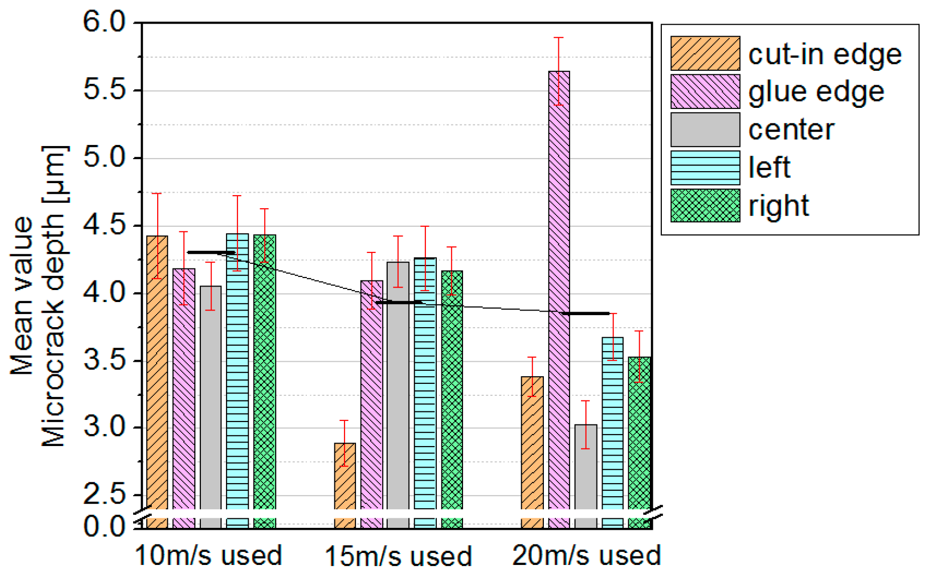
3.3. Determination of Microcrack Depths

The sub-surface damage mainly consists of microcracks [1,11]. The depth of the microcracks can be influenced by the sawing process parameters and particularly depends on wire velocity and wire wear.
The maximum microcrack depths on the three wafers with wire velocities of 10 m/s, 15 m/s and 20 m/s taken from the end of the brick, where the used wire leaves the cutting zone, were measured by CLSM. Polished and etched bevel-cut samples were prepared for the five wafer positions on each wafer.
Figure 10 gives an overview of the microcrack depth at the analyzed positions on each wafer as a column diagram. Based on this representation, it can be observed that the crack depth decreases with increasing wire velocity. As mentioned in [9], this behavior also correlates with lower forces in the sawing direction for higher wire velocities at a constant feed rate of the silicon ingot. Higher wire velocities could induce more material removal in the wire sawing direction, causing shallower depth damage.
The slowest sawn wafer (10 m/s) from the used wire side is characterized by a higher number and larger length of microcracks compared to the fastest sawn wafer (20 m/s). The total stress was more reduced (and the stress difference ∆σ was enhanced) by the slowest sawing, and deeper crack structures were induced.
Generally, the crack depths range between 1.1 µm and 13.2 µm. Obviously, the cracks in the center position are often less deep (except for 15 m/s used). Additionally, the stress level at these positions is increased. The number of cracks and their depths determine the degree of stress reduction [12].

4. Summary and Conclusions

The sub-surface damage of diamond wire-sawn monocrystalline silicon wafers with respect to the process parameters of wire velocity and wire cutting ability was investigated. Wafers sawn with three different wire velocities (10, 15 and 20 m/s) were analyzed. The silicon ingot feed rate was kept constant during the sawing process. Wafers were taken from brick positions at the wire entry (fresh wire side) and wire exit side (used wire side) to examine the wire wear. Measurements of the intensity ratio r of the amorphous to crystalline silicon phase (a-Si/c-Si), surface damage shown by stress imaging and microcrack depth were performed on all wafer surfaces. The crack depths were determined by confocal laser scanning microscopy on bevel-cut samples. To characterize the sub-surface damage, Raman spectroscopy and SIREX polarimetry were used as independent, non-destructive, contactless, high-resolution optical stress imaging methods. The SIREX results yield the difference σ1σ2 between the main stress components and thereby visualize the stress anisotropy, while the Raman measurements yield the absolute in-plane stresses. The SIREX system allows for higher measuring velocities than Raman spectroscopy, whereas the amorphous silicon phases on wafer surfaces can only be detected with Raman. Thus, the two characterization methods are complementary.
The results of the Raman investigations reveal unevenly distributed layers of amorphous silicon phase on the surface of diamond wire-sawn wafers. The fraction of the amorphous phase (r-value) and the homogeneity of the stress distribution on wafers are found to be connected to both the wire wear and the wire velocity:
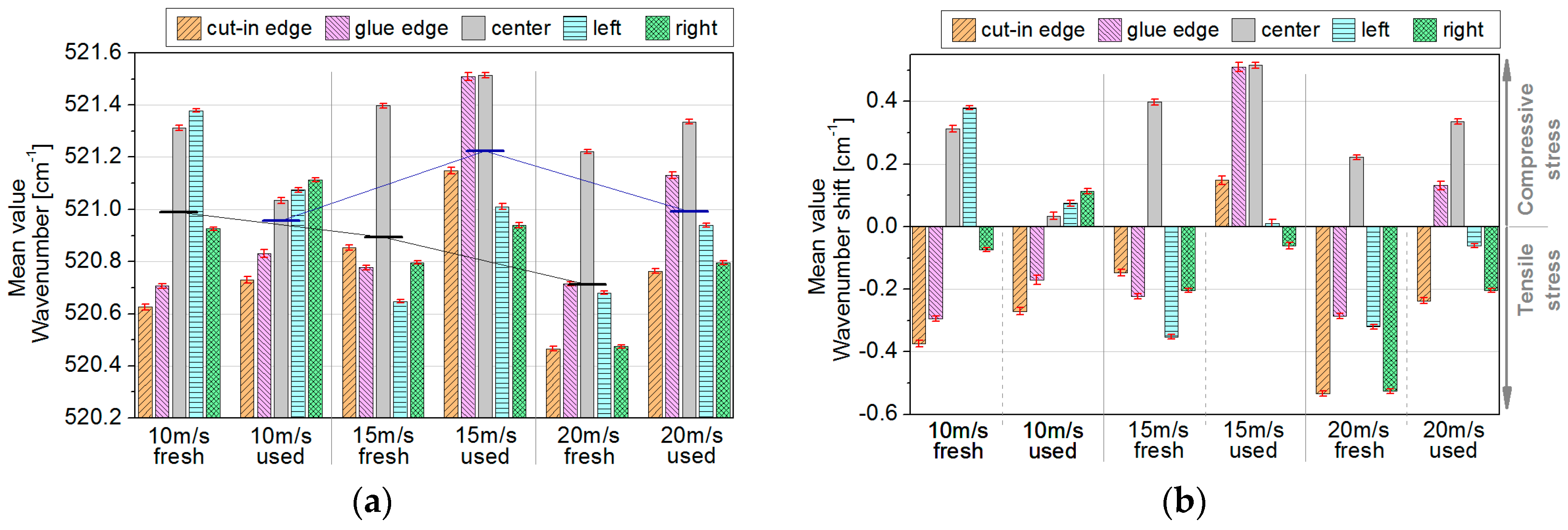
  • A lower Raman intensity ratio r (a-Si/c-Si ratio) correlates with a more homogeneous stress distribution.
    -
    A lower amount of a-Si phase occurs at the cut-in side of the wafer from the used wire side.
    -
    Lower a-Si is present at the wafer center from the used wire side compared to the left and right wafer edges.
    -
    Lower amorphization occurs on wafers from the fresh wire side.
    -
    Lower a-Si occurs on the wafer surface due to sawing with a lower wire velocity.
The sawn wafers from the used wire side indicate locally intensified compressive stresses parallel to the sawing grooves, up to 1.8 GPa. Generally, the wafer center seems to be more compressively stressed than the areas at the wafer edges. The stresses near the cut-in edge, where the wire is fresh, are higher than at the gluing edge.
The distribution between a-Si and c-Si is related to the material removal process of chipping. More chipping reduces the fraction of a-Si. The degree of the amorphization can be qualified as an indication of the wire wear. So, the results show lower amorphization on wafers of the fresh wire side and close to the cut-in edge. During sawing with fresh wires, where the diamond edges are sharp and exhibit good cutting performance, the grain contact area with the silicon material is smaller than for the worn grains on used wires, and therefore, shallow damage with more material chipping is caused. In addition, the amount of the a-Si fraction on the wafer surface depends on the wire velocity. One explanation is the behavior of silicon under stress [13]. Under slow pressure relief of the silicon material, a mixture of crystalline phases is produced, whereas with faster relief, the crystalline silicon becomes amorphous. Therefore, one can expect slowly sawn wafers to exhibit a lower amorphous to crystalline silicon ratio than faster sawn ones.
The SIREX photo-elastic microscope was presented as a new approach to evaluate the sub-surface damage and the related sawing processes by characterizing the sub-surface stress. SIREX polarimeters can reveal the in-plane differences of the principal stress components ∆σ. For this purpose, a measurement procedure was used in which the initial polarization varies with respect to the stress field direction in the wafer. In this way, the visualization of the anisotropy of the sub-surface stress shows a clear relation to the saw grooves. Line scans of ∆σ taken across the saw grooves at different positions on the wafer show significant differences in magnitude and periodicity. The stress differences ∆σ show a connection with the wire wear and wire velocity. This result confirms that the degree of sub-surface stress generated in the course of the sawing process changes. The following essential results could be shown:
  • Lower ∆σ peak maxima correspond to a higher amorphization of the silicon surface.
    -
    Lower ∆σ values occur at the gluing edge side of the wafer compared to the cut-in side.
    -
    Lower stress values occur on wafers cut by used wires.
    -
    The stress difference tends to be lower when sawing with a higher wire velocity.
Furthermore, the analysis of the microcrack depth on bevel-cut samples shows a relation with the wire wear and wire velocity:
  • A lower microcrack depth shows a tendency toward higher stress.
    -
    Lower crack depth with higher crack number and higher stress occurs at the wafer cut-in side.
    -
    Lower damage by microcracks arises from sawing with a higher wire velocity.
Higher wire velocities correlate with lower forces in the sawing direction (for constant feed rate) and could induce more material removal in the wire sawing direction, causing lower depth damage. Fresh sawing wires with sharp diamond grains induce a different crack structure and stress level compared to sawing with used wires, where the diamonds are worn. The following application-oriented conclusions have been reached:
(1)
Sawing with fresh diamond wire induces lower depth damage with shallower cracks. Reducing the crack length increases the fracture strength. Additionally, the fraction of the amorphous silicon on the wafer surface is smaller compared to sawing with diamond wire with worn particles. However, the maximal measured stress difference is higher on the fresh wire wafer side.
(2)
Sawing with higher wire velocity (reduction of the forces in the sawing direction under a constant feed rate) results in a lower crack depth. However, the local amorphization of the silicon surface is increased.
Furthermore, the cleaning step after sawing influences the thickness of the amorphous layer on the wafer surface. In [9], it was observed that in our standard cleaning procedure, approximately 50% of the surface amorphization present after sawing is etched away by the chemical process. This result suggests that the degree of surface amorphization could affect the texture etching performance. If so, the amorphization on the wafer surfaces can be reduced by sawing with fresh wire at a lower wire velocity.

Acknowledgments

Thanks to the entire wafer technology group at the Fraunhofer THM for their support.

Author Contributions

Sindy Würzner performed the Raman measurements and the analyses of the microcrack depth; Martin Herms performed the SIREX measurements; Sindy Würzner and Martin Herms analyzed and interpreted the data; Thomas Kaden, Hans Joachim Möller and Matthias Wagner contributed to the interpretation of data; Sindy Würzner wrote the paper.

Conflicts of Interest

The authors declare no conflict of interest.

References

  1. Würzner, S.; Buchwald, R.; Möller, H.J. Surface damage and mechanical strength of silicon wafers. Phys. Stat. Sol. C 2015, 12, 1119–1122. [Google Scholar] [CrossRef]
  2. Würzner, S.; Buchwald, R.; Retsch, S.; Möller, H.J. Investigation of the development of the microcrack structure in scratch tests with single diamond particles on monocrystalline silicon wafers. In Proceedings of the 29th European Photovoltaic Solar Energy Conference and Exhibition (EU PVSEC 2014), Amsterdam, The Netherlands, 22–26 September 2014; pp. 742–746. [Google Scholar]
  3. Möller, H.J.; Würzner, S.; Buchwald, R.; Herms, M.; Wagner, M. Comparative investigations of the surface damage of monocrystalline silicon wafers by Scanning Infrared Reflection Examination and Raman spectroscopy. Solid. State Phenom. 2016, 242, 466–471. [Google Scholar] [CrossRef]
  4. Geiler, H.D.; Karge, H.; Wagner, M.; Eichler, S.; Jurisch, M.; Kretzer, U.; Scheffer-Czygan, M. Photoelastic characterization of residual stress in GaAs-wafers. Mater. Sci. Semicond. Process. 2006, 9, 345–350. [Google Scholar] [CrossRef]
  5. Wolf, I.D. Micro-Raman spectroscopy to study local mechanical stress in silicon integrated circuits. Semicond. Sci. Technol. 1996, 11, 139–154. [Google Scholar] [CrossRef]
  6. Becker, M.; Scheel, H.; Christiansen, S.; Strunk, H.P. Grain orientation, texture, and internal stress optically evaluated by micro-Raman spectroscopy. J. Appl. Phys. 2007, 101, 063531. [Google Scholar] [CrossRef]
  7. Gogotsi, Y.; Baek, C.; Kirscht, F. Raman microspectroscopy study of processing-induced phase transformations and residual stress in silicon. Semicond. Sci. Technol. 1999, 14, 936–944. [Google Scholar] [CrossRef]
  8. Yan, J.; Asami, T.; Kuriyagawa, T. Nondestructive measurement of machining-induced amorphous layers in single-crystal silicon by laser micro-Raman spectroscopy. Precis. Eng. 2008, 32, 186–195. [Google Scholar] [CrossRef]
  9. Würzner, S.; Falke, A.; Buchwald, R.; Möller, H.J. Determination of the impact of the wire velocity on the surface damage of diamond wire sawn silicon wafers. Energy Procedia 2015, 77, 881–890. [Google Scholar] [CrossRef]
  10. D’Aragona, F.S. Dislocation etch for (100) planes in silicon. J. Electrochem. Soc. 1972, 119, 948–951. [Google Scholar]
  11. Buchwald, R.; Würzner, S.; Fröhlich, K.; Winstanley, S.; Lehmann, T.; Sunder, K.; Möller, H.J. Analysis of the sub-surface damage of mc- and cz-si wafers sawn with diamond-plated wire. In Proceedings of the 28th European Photovoltaic Solar Energy Conference and Exhibition (EU PVSEC 2013), Paris, France, 30 September–4 October 2013; pp. 1502–1506. [Google Scholar]
  12. Behm, T.; Fütterer, W.; Funke, C.; Kaminski, S.; Möller, H.J.; Rietzschel, R.; Wagner, T. Challenges of the wire saw wafering process. Photovol. Int. 2011, 11, 36–47. [Google Scholar]
  13. Domnich, V.; Gogotsi, Y. Phase transformations in silicon under contact loading. Rev. Adv. Mater. Sci. 2002, 3, 1–36. [Google Scholar]
Figure 1. Schematic of a wafer (156 × 156 mm2) indicating the positions of the characterized areas (green marked) for investigation of sub-surface stresses, amorphization and microcrack depths.
Energies 10 00414 g001
Figure 2. Raman intensity ratio r of five different wafer positions for wafers of the (a) fresh and (b) used wire side sawn with 10 m/s, 15 m/s and 20 m/s wire velocity (r mean value of 2600 Raman spectra with standard error of the mean).
Energies 10 00414 g002
Figure 3. Mappings of the Raman shift of crystalline silicon peaks of the fastest sawn wafer (20 m/s) from (a) the fresh wire and (b) the used wire side. Both measurements were conducted near the gluing edge of the wafer.
Energies 10 00414 g003
Figure 4. Normalized relative frequencies of the Raman c-Si wave number range for the measured upper wafer positions near the gluing edge.
Energies 10 00414 g004
Figure 5. (a) Raman c-Si wave number mean values and (b) Raman shift with respect to the c-Si peak at 521 cm−1 for all measured areas on the wafers (mean value of 2600 Raman spectra with standard error of the mean). The horizontal lines show the c-Si wave number peaks averaged over the five wafer positions.
Energies 10 00414 g005
Figure 6. Calculated ∆σ maps from SIREX measurements on the slowest diamond-sawn wafer (10 m/s) from the used wire side. Topogram (a) is the result for the analyzed position near the cut-in edge and topogram (b) for the position close to the gluing edge. Optical (CLSM) images of a section within the SIREX topogram for (c) cut-in and (d) glue edge position.
Energies 10 00414 g006
Figure 7. Histogram of ∆σ maps for the slowest sawn wafer (10 m/s) from the used wire side. The inset shows the ∆σ range from 2 to 5 MPa with logarithmic scale of the axis of ordinate.
Energies 10 00414 g007
Figure 8. (a) ∆σ line scans across the saw grooves at the five measured positions on the slowest sawn wafer (10 m/s) from the used wire side. Data of the line scans of cut-in edge and glue edge from ref. [3] were supplemented by further positions on the wafer; (b) Column diagram of the ∆σ peak maximum determined from the histograms for all measured areas on the wafers (most frequent value of at least 34,000 histogram data with the given systematic error of the method). The horizontal lines show the peak maxima of ∆σ averaged over the five wafer positions.
Energies 10 00414 g008
Figure 9. Maximum ∆σ values from SIREX measurements in relation to Raman intensity ratios r of a-Si/c-Si.
Energies 10 00414 g009
Figure 10. Microcrack depths for all measured areas on the wafers from the used wire side (mean value of 40 crack depths with standard error of the mean). The horizontal lines show the microcrack depths averaged over the five wafer positions.
Energies 10 00414 g010
Table 1. Overview of the main process parameters for the diamond sawing of the characterized monocrystalline silicon wafers here.
Parameter NameParameter Value
Type of wire sawMeyer Burger DS264
Wire core diameter120 µm
Diamond size distribution8–16 µm
Linear diamond density330 diamonds per mm2 wire surface
Coolant mediumneutral water based coolant
Wire velocities10 m/s; 15 m/s; 20 m/s
Pilgrim length322 m forward/319 m backward
Wire tension28 N
Feed rate0.6 mm/min
Table 2. Overview of amorphous to crystalline silicon ratios r on the wafer surfaces. The values represent the mean of five wafer positions. The amorphous layer depth is given in parentheses.
Wire VelocityRaman Intensity Ratio r for Wafers of the
Fresh Wire SideUsed Wire Side
10 m/s0.16 (8 nm)0.58 (23 nm)
15 m/s0.21 (10 nm)1.29 (38 nm)
20 m/s0.25 (12 nm)1.13 (35 nm)

