Article

EMTP Model of a Bidirectional Cascaded Multilevel Solid State Transformer for Distribution System Studies

by
Jacinto Martin-Arnedo
1,
Francisco González-Molina
2,
Juan A. Martinez-Velasco
3,* and
Mohammad Ebrahim Adabi
3
1
Estabanell Energia, 08401 Granollers, Spain
2
Departament d’Enginyeria Electrònica, Elèctrica i Automàtica, Universitat Rovira i Virgili, 43007 Tarragona, Spain
3
Departament d’Enginyeria Elèctrica, Universitat Politècnica de Catalunya, 08028 Barcelona, Spain
*
Author to whom correspondence should be addressed.
Energies 2017, 10(4), 521; https://doi.org/10.3390/en10040521
Submission received: 30 January 2017 / Revised: 10 March 2017 / Accepted: 10 April 2017 / Published: 12 April 2017
(This article belongs to the Special Issue Electric Power Systems Research 2017)

Abstract

:
This paper presents a time-domain model of a MV/LV bidirectional solid state transformer (SST). A multilevel converter configuration of the SST MV side is obtained by cascading a single-phase cell made of the series connection of an H bridge and a dual active bridge (dc-dc converter); the aim is to configure a realistic SST design suitable for MV levels. A three-phase four-wire converter has been used for the LV side, allowing the connection of both load/generation. The SST model, including the corresponding controllers, has been built and encapsulated as a custom-made model in the ATP version of the EMTP for application in distribution system studies. Several case studies have been carried out in order to evaluate the behavior of the proposed SST design under different operating conditions and check its impact on power quality.

1. Introduction

The solid state-transformer (SST) is foreseen as a replacement of the conventional transformer and a fundamental component of the future smart grid. Utilities can expand traditional services by integrating various power requirements, monitoring, and communications into a universal customer interface such as the SST. The SST offers several benefits for the future development of the smart grid [1,2,3,4]: enhanced power quality performance, fast voltage control, reactive power compensation or reactive power control at both primary and secondary sides, dc and high-frequency ac power supply. The SST can also provide some operational benefits, such as an efficient management of distribution resources by incorporating on-line monitoring and other distribution automation functionalities.
The SST is a very flexible device that can be used as a link between standard ac power-frequency systems and systems operating with either dc or ac at any power frequency [5]. It can be seen as a universal interface that can provide not only power quality improvements but efficient management of distribution resources.
This paper proposes a realistic model of a three-phase multilevel SST design for Electro Magnetic Transient Program (EMTP) implementation [6]. The SST design analyzed here provides a device that can cope with bidirectional power flow between two power-frequency ac distribution systems operating respectively at medium and low voltages. The proposed SST design has been built in the ATP version of the EMTP as a custom-made model; so it can be used as a built-in component by ATP users interested in distribution system studies.
Since standardized voltages used by most utilities for medium voltage (MV) distribution grids are usually equal or higher than 10 kV [7], multilevel topologies must be considered for the MV side of the SST if conventional Si-based semiconductors are used; see [8,9,10]. Actually, with the safety factor usually applied when selecting power semiconductors for high-voltage applications, more than ten levels can be required if Si-based semiconductors with a blocking voltage of less than 2 kV are used for rated line voltages above 10 kV rms [11].
A previous work [12] presented the model of a multilevel SST design based on the neutral-point-clamped (NPC) topology. However, the number of levels assumed for the MV side converter of that model limited the connection to distribution grids with reduced voltage. Therefore, in order to allow the connection to distribution grids with standardized voltages, that configuration has been replaced by a topology based on the single-phase cascaded H bridge configuration analyzed in [13,14].
The paper is organized as follows: the topology selected for a bidirectional multilevel SST design as well as the control strategies are presented in Section 2. Section 3 presents the system used in this work for testing the behavior of the implemented SST model, and several simulation results that verify the validity of the SST and confirm its enhanced behavior in comparison to the conventional transformer. Main conclusions and future development are summarized in Section 4.

2. Solid State Transformer Configuration and Switching Strategies

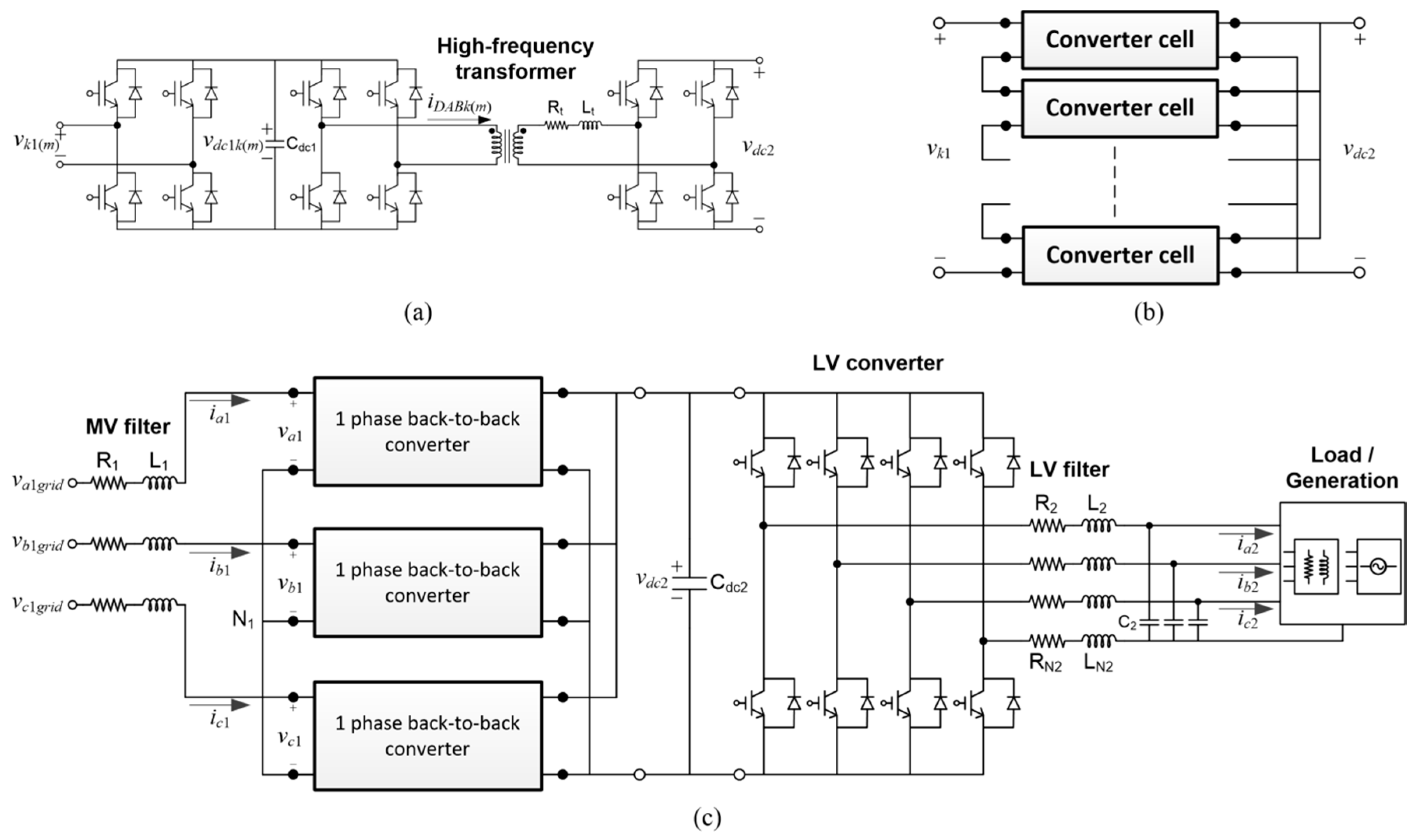
2.1. SST Configuration

The proposed bidirectional SST design is based on the commonly accepted three-stage design [15,16,17,18]: (1) the input voltage at power frequency is first converted into dc voltage by the MV-side three-phase converter working as rectifier; (2) the isolation stage is implemented by means of a dual active bridge (DAB) dc-dc converter, with an intermediate high-frequency transformer that reduces the MV square waveform into a LV square waveform; (3) a low voltage (LV) three-phase dc/ac converter working as inverter provides the output power-frequency ac voltage to LV loads.
Since in real systems generation could be connected to the secondary side of the transformer, the LV side should be able to operate in generation mode to allow the power to flow from the secondary LV side to the primary MV side. The SST behavior will be then similar to that described above; basically, input and output stages swap functions. Therefore, the converters and their respective switching strategies must be properly designed to work under bidirectional power flow conditions.
The implemented topology for the MV side is based on the cascaded connection of single-phase cells proposed or studied in several papers; see for instance [13,14,19,20,21]. The configuration selected for the basic cell is the single-phase DAB converter presented in [13,14], although the present model incorporates some changes in the control strategies and the MV-side design is three-phase, while the configuration used in [13,14] was single-phase. As for the LV side, it is based on the three-phase four-wire configuration and control strategy implemented by the authors in some previous works; see [15,17].
Figure 1a shows the configuration of the converter cell that would be the base of the modular design implemented in this work. Note that the cell consists of an input single-phase H bridge and an isolation stage made by a DAB dc-dc converter. Each single phase section of the SST is made out of a number of basic cells that will depend on the voltage level, being the configuration the result of cascading in series the primary MV side of the converter cell and connecting in parallel the secondary LV side, see Figure 1b. The proposed design consists of an ungrounded star connection of the three single-phase SST primary sides, see Figure 1c. The outputs of all dual active bridges are connected in parallel to the LV-side dc bus. As already mentioned, the LV converter feeds a three-phase four-wire system to which both load and generation can be connected, see Figure 1c.

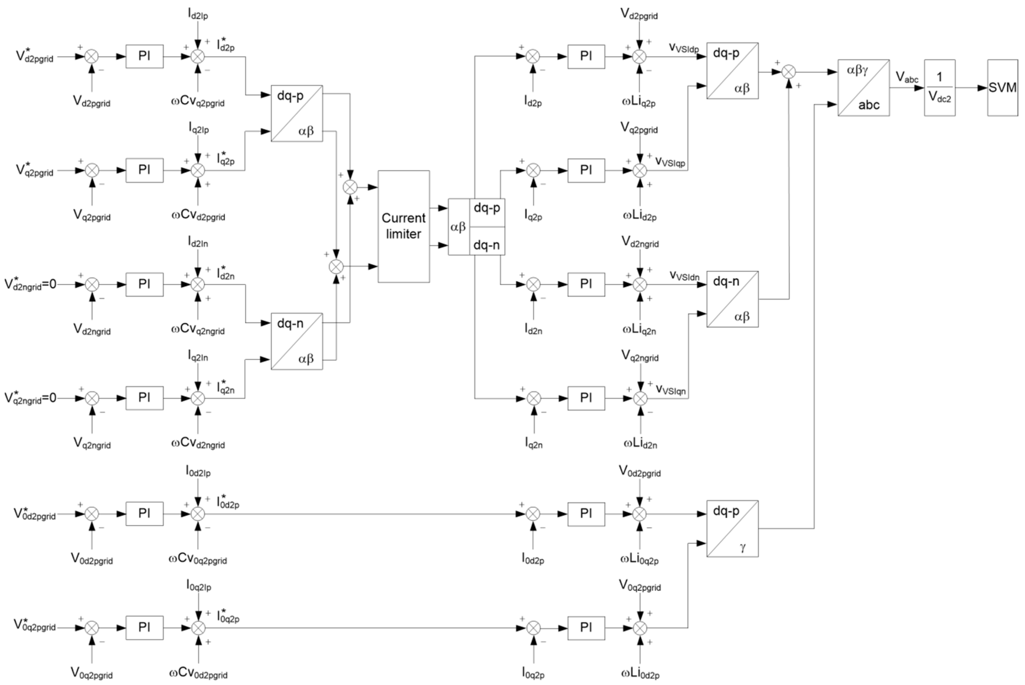
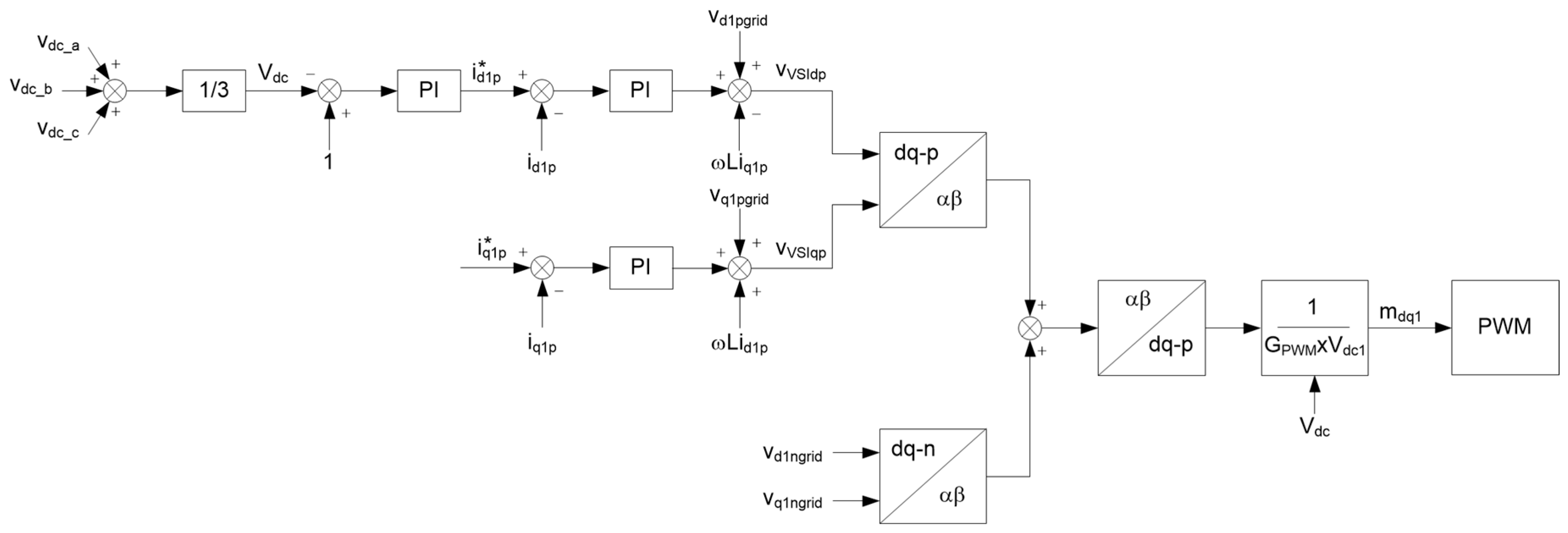
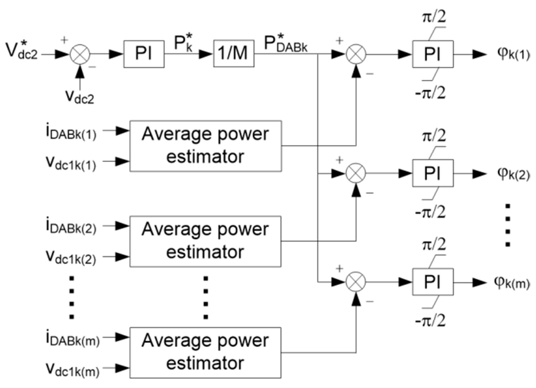
2.2. Switching Strategies and Control Description

Although the SST design proposed in this paper is based on a cascaded multilevel connection at the MV side, it is still acceptable considering a three-stage configuration (MV-level input, isolation and LV-level output stages). However, the configuration shown in Figure 1 implies that there will be as many input and isolation stages as single-phase cells are needed to build the final design (see Figure 1a). In addition, since it is assumed that all basic single cells are equally rated, the controllers have to achieve a homogeneously distributed voltage across all of them (i.e., voltages across each Cdc1 in Figure 1a must be as equal as possible). Note that, given the series connection at the MV side, the current across any basic single cell is the same that in the corresponding phase of the MV level grid.
The control strategies used for each stage as well as the controller required to voltage balance are summarized below.
Input stage: The control strategy for any single cell follows the principles used in some previous works, see [15,17]. The input stage is implemented by means of a multilevel converter; see, for instance [13,20]. The abc-frame model for the converter is as follows (see Figure 1):
v k 1 g r i d = R 1 i k 1 + L 1 d d t i k 1 + v k 1 + v N 1
v k 1 = m = 1 M v k 1 ( m )
where ka, b, c, vk1grid are the MV-side abc distribution system voltages at the point of coupling, ik1 are the MV-side abc distribution system currents, vk1 are the MV-side abc single-phase converter voltages, vk1(m) are MV-side abc cell voltages, M is the number of cells that compose each single-phase MV-side converter, vN1 is the MV distribution system neutral, R1 and L1 are respectively the MV-side filter resistance and inductance.
The three-phase PWM converter obtained by applying the Park transform to Equation (1a) may be represented by the following model:
d d t i d 1 = ω 1 i q 1 R 1 L 1 i d 1 + 1 L 1 v d 1 c o n v 1 L 1 v d 1 g r i d
d d t i q 1 = ω 1 i d 1 R 1 L 1 i q 1 + 1 L 1 v q 1 c o n v 1 L 1 v q 1 g r i d
where id1, iq1 are the MV side grid currents in the rotating dq-frame, vd1conv, vq1conv are the MV-side converter voltages in the rotating dq-frame, vd1grid, vq1grid are the MV-side grid voltages also in the rotating dq-frame, ω1 is the MV-side grid angular frequency, R1 and L1 are respectively the resistance and inductance of the MV-side filter.
For conventional control of this converter, there are an outer dc-link voltage control loop and an inner grid current control loop to achieve high dynamic response and stability (see Figure 2); the inner grid current control loop provides fast compensation for input supply disturbances. The reference for the grid current loop is given by the output of the outer dc-link voltage control loop. Figure 2 shows how the reference for the positive-sequence current value is obtained from the per unit deviation of the dc link voltage average value with respect to the desired voltage.
A simple and effective strategy, the voltage oriented control (VOC), with feedforward of the negative-sequence grid voltage, has been applied in this work to control the MV-side converter [22]. A sequence separation method is applied to the grid voltages:
  • The positive-sequence grid voltage is used to obtain the grid angle for synchronization purposes by means of a phase-locked loop (PLL) [23].
  • The negative-sequence grid voltage is fed-forwarded to the switching strategy that has to be generated at the converter terminals; therefore, no negative sequence voltage is seen by the inductive filter and only positive-sequence currents flow between the grid and the converter, even in presence of asymmetrical grid disturbances; see Figure 2.
This scheme ensures constant dc bus voltage, unity power factor condition at the input terminal in an average sense, and no ripple in the input active power. As shown in Figure 2, all the controllers have been implemented with conventional PI regulators. Because of the coupling between the d- and q-components of the grid currents, a conventional solution of adding two decoupling feed-forward inputs to each current control loop has been considered. The selection of parameters is following the proposal presented in [24].
Since a single-phase section of the three-phase MV side is made by cascading single-phase cells, see Figure 1, the voltage has to be uniformly distributed among the dc buses which are part of the topology implemented for the MV converter. A simple balance controller for the parallel operated DAB converters is used [13,14]. The MV-side dc link voltage of each module is selected as the feedback signal for the controller, being the reference V d c 1 * a predefined value. By default, it is assumed that the total voltage is equally shared among the modules, although the controller assumes that there can be parameter mismatch (see below). In order to achieve voltage balancing among the dc links of each phase, a modification of the duty cycle, Δd, is added to the common duty cycle for each H-bridge (see Figure 3).
Δ d 1 ( m ) = ( K p 1 + K i 1 s ) ( V d c 1 * v d c 1 ( m ) )
A voltage balance among dc buses with the new duty cycle generated for each single-phase cell will also guarantee a power balance among the DAB converters: due to the series connection of the cells of each phase, the current that flows through each H-bridge cell is the same, therefore the power among the DAB converters will be balanced if the voltage balance is achieved. Note that the strategy depicted in Figure 3 guarantees that the new duty cycles will add to the same quantity that was previously used and, therefore, assures the same value of the total DC link voltage.
Isolation stage: The amount and direction of the active power flow between primary and secondary of each high-frequency transformer is according to the following expression [25] (see also [15,16,17]):
P k ( m ) = v d c 1 k ( m ) v d c 2 2 π f r L t φ k ( m ) ( 1 | φ k ( m ) | π )
where vdc1k(m) and vdc2 are the MV- and LV-side voltages of the dual active bridge, r is the turns ratio of the transformers, f is the switching frequency of the converters, Lt is the transformer impedance value seen from the secondary side, and φk(m) is the phase between primary and secondary side voltages of the dual active H-bridge, being ka, b, c, and 1 ≤ mM.
When more than a single DAB converter is used in parallel, as in Figure 1b, it has been observed that if the same phase shift is adopted for all DAB converters and the voltages in the MV-side dc links are regulated to the same value, a mismatch of parameters (e.g., transformer leakage inductances) can cause an unbalanced power share among them [13,14]. Therefore, different phase shift may be needed for each DAB converter to ensure the power balance. The power balance controller is shown in Figure 4. The average power of each DAB converter is calculated and compared to the overall average, so a different phase shift can be generated for each of them if required. The dc-dc converter makes the power to flow towards the end-user side when voltage at the primary side of the transformer leads voltage at the secondary side. Power flows towards the MV distribution network when the voltage at the secondary side leads the voltage at the primary side. The absolute value of this reference phase-shift angle φ is limited to π/2, irrespective of the sense in which power flows.
Output stage: The LV side front-end converter includes a fourth leg for neutral currents, an inductor for filtering currents and a capacitor bank for filtering voltages. According to the configuration shown in Figure 1c the LV-side converter may be connected to load and/or generation, and it is responsible for controlling the voltage (waveform and value) seen by load/generation. The three-phase four-wire LV converter allows connecting loads and/or generators with either one, two or three phases. A Space Vector Modulation (SVM) PWM switching strategy has been used in the LV-side converter, see Figure 5 and references [15,17,26].
The main task of the LV-side converter controllers is to achieve positive-sequence capacitor voltages (i.e., to have balanced voltages at capacitor terminals) with stable frequency and voltage, independently of the power direction (i.e., load or generation) and the current balance. Each positive-, negative- and zero-sequence has its respective controller. Negative- and zero-sequence capacitor voltage references are set to zero to cancel these components at the filter capacitor terminals at all time, even in presence of unbalanced load/generation currents. The positive sequence voltage controller regulates the filter capacitor voltages. For more details about the control strategy see [15,17]. The controller shown in Figure 5 includes a current limiter that prevents the current peak caused during either an overload or a short-circuit from exceeding a specified value. Note that the limiting effect is performed in the αβ synchronous reference frame and does not affect the zero-sequence component of the current.
The limit of the peak currents specified in the simulation model, ilim, is compared to the following value (see Figure 5):
i p e a k = i α 2 + i β 2
If ipeak exceeds the specified ilim then the dq values are obtained from the values iα and iβ that result from changing ipeak to ilim. For more details on the application of three-phase four-leg converters and their control strategies, see [27,28,29].

3. Testing the Performance of the SST Model

This section details the modeling guidelines followed to implement the test system and the SST models in ATP, and provides a summary of the simulation results obtained when testing the SST as a device adequate for solving power quality issues.

3.1. Test System and Modeling Guidelines

The test system model developed for this work is a 50 Hz overhead distribution system based on previous models developed by the authors; see [12]. Figure 6 shows the configuration of the network, per unit length parameters and lengths of all line sections. Note that all line sections of the test system have the same per unit length parameters. The delta-connected MV side of the substation transformer is grounded by means of a zig-zag reactor. The figure also indicates the node to which the SST is connected and the fault location considered in the first case study, but it does not show the system loads.
The model has been implemented in the ATP version of the EMTP following the guidelines recommended when using EMTP-like tools; see for instance [30,31]: the semiconductors are modeled as ideal controlled switches and the controllers have been implemented using TACS (Transient Analysis of Control Systems) capabilities. The high-frequency transformer is represented as an ideal transformer in series with its short-circuit impedance. Each single-phase section of the MV side (see Figure 1b) is made of six basic cells (see Figure 1a). Taking into account the current semiconductor technology, this number is probably low for a realistic design of a multilevel converter that should be connected to a 12 kV grid; actually about eight to ten cascaded cells would be recommendable to withstand the stresses to which MV side semiconductors could be subjected [11]. The number of basic cells has been reduced in this work to six in order to decrease the computing time that is required and because such quantity suffices to check the validity of the voltage balancing control strategy. See also the Discussion.
The SST model has been encapsulated as a custom-made model, so users do only have to connect MV and LV terminals to the distribution system and load models, and specify SST parameters. Rated values of primary and secondary SST voltages are respectively 12 kV and 400 V. The case studies presented below were carried out assuming that the rated power of the SST is 100 kVA. Table 1 presents the main parameters used in this study.
The parameter values of the high-frequency transformer in Table 1 are referred to its secondary side. The system loading is such that the steady-state voltage at the node to which the SST is connected is below 0.95 p.u. in all case studies detailed in the next subsection. The controller of the MV-side converters will compensate the reactive power at the MV terminals of the SST; that is, reactive power will be close to zero under steady-state operating conditions and deviate from the zero value during transients.

3.2. Case Studies

Several case studies have been carried out to illustrate the performance of the new SST model. The cases have been selected taking into account those presented in previous works [12,15,16,17]. Figure 7, Figure 8, Figure 9 and Figure 10 depict the main results of each case study. All figures show the same plots: voltages, currents and powers measured at both MV and LV SST terminals. A short analysis of each case study is provided below.
(i)
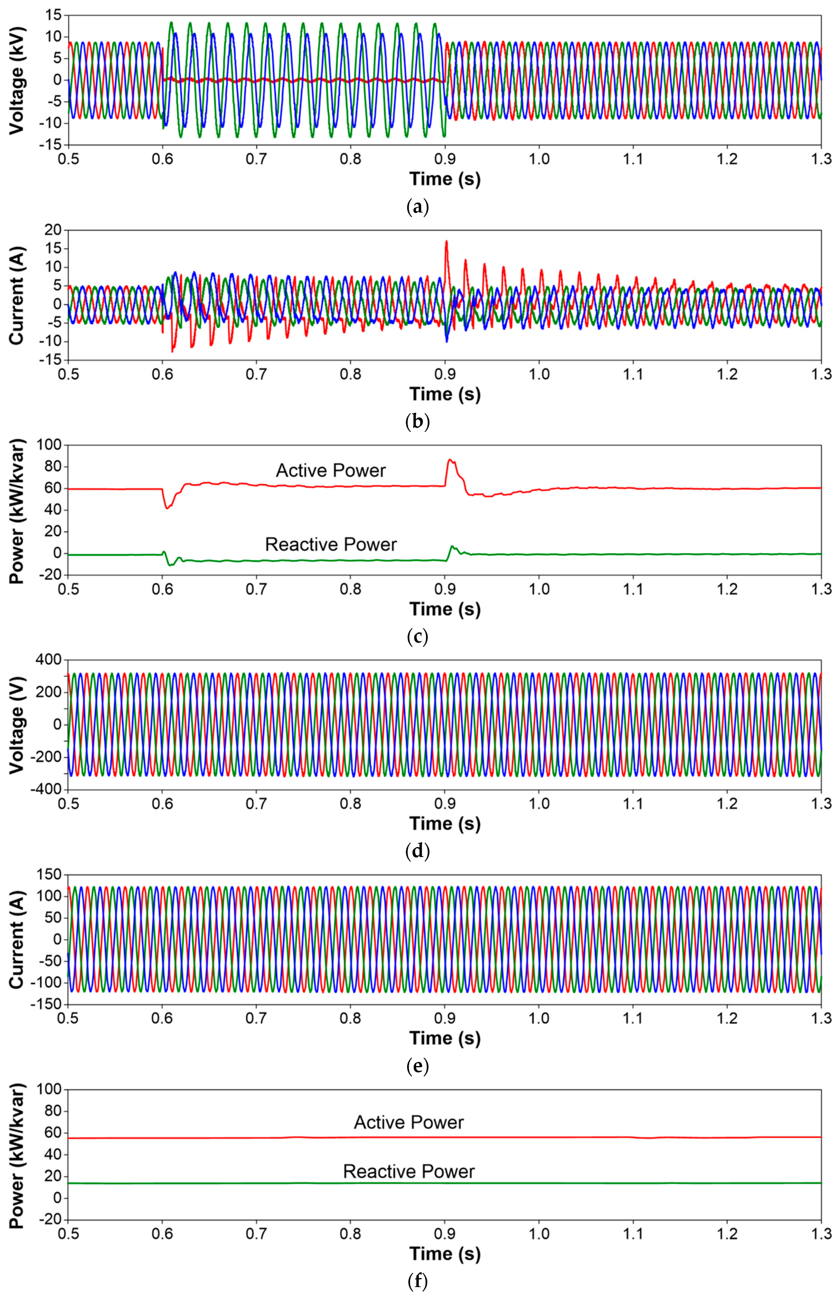
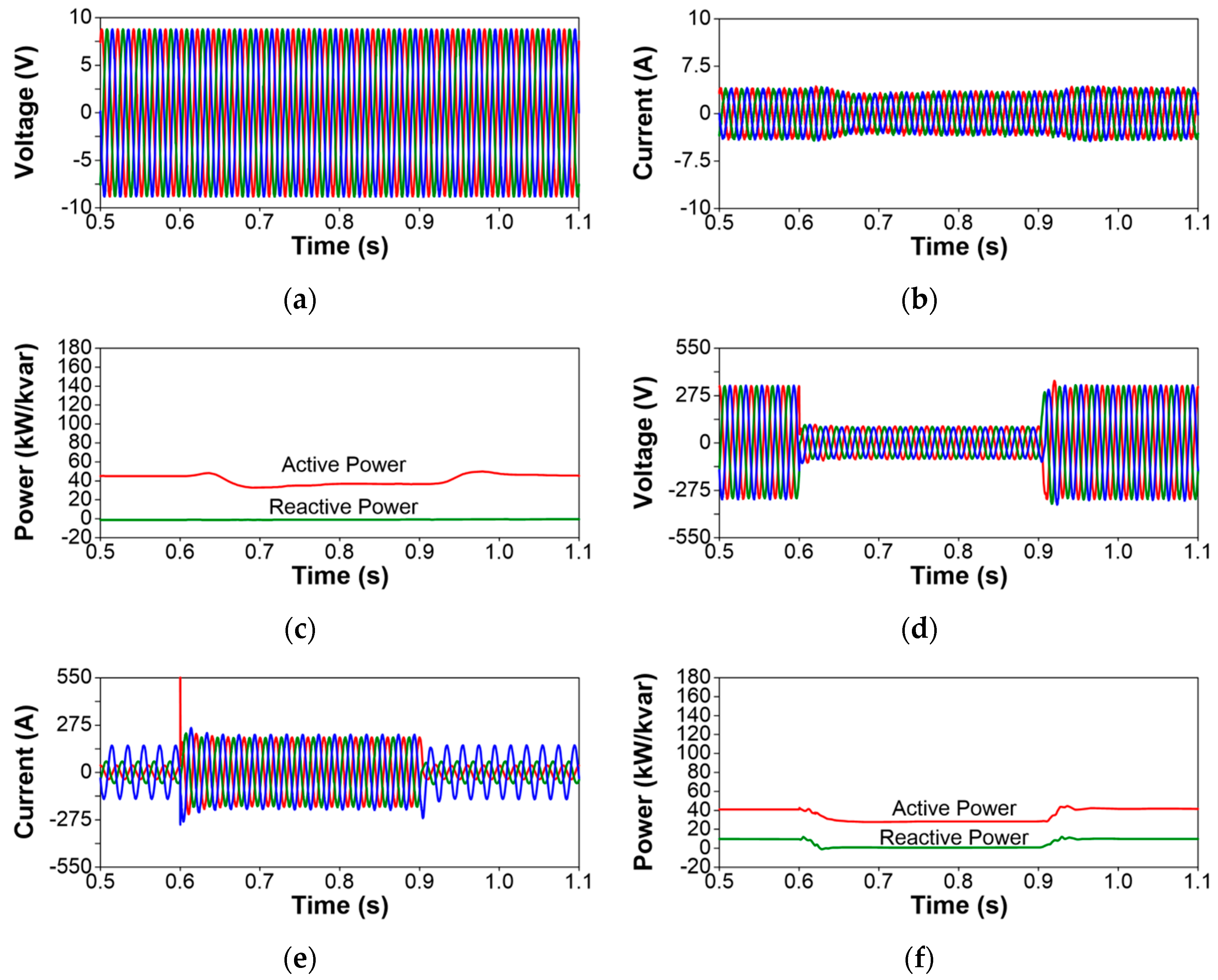
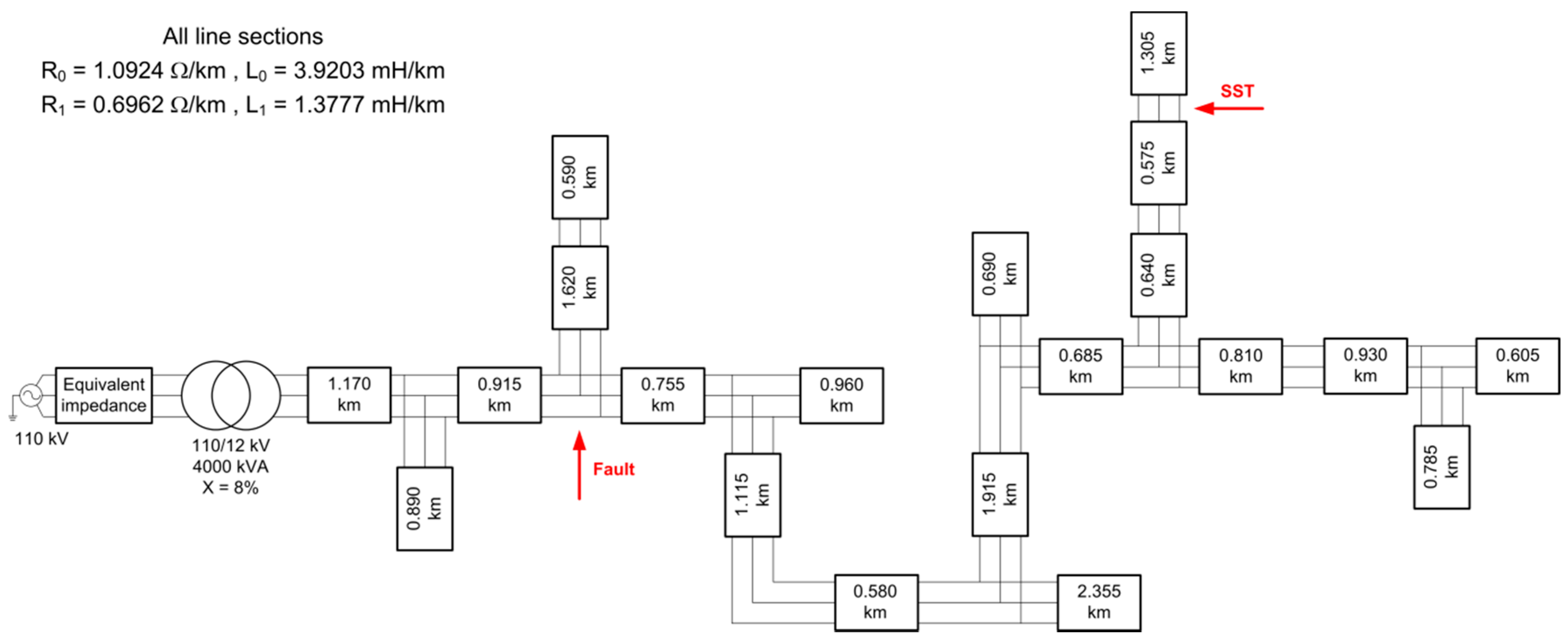
Voltage sags and swells at MV terminals: Due to the grounding system selected for the test system, a single-phase-to-ground fault in the MV network (see fault location in Figure 6) will cause a voltage sag at the faulted phase MV terminals of the SST, and two voltage swells at the unfaulted phase terminals. The simulation results related to this case (see Figure 7) prove clearly that the voltage unbalance that occurs in the primary side of the SST is not propagated to the secondary side, where the phase voltages and currents remain constant and balanced. Note that the peak values of the currents during the fault condition are lower in the SST phases in which the fault causes swells and that the SST recovers current balance once the fault condition disappears.
(ii)
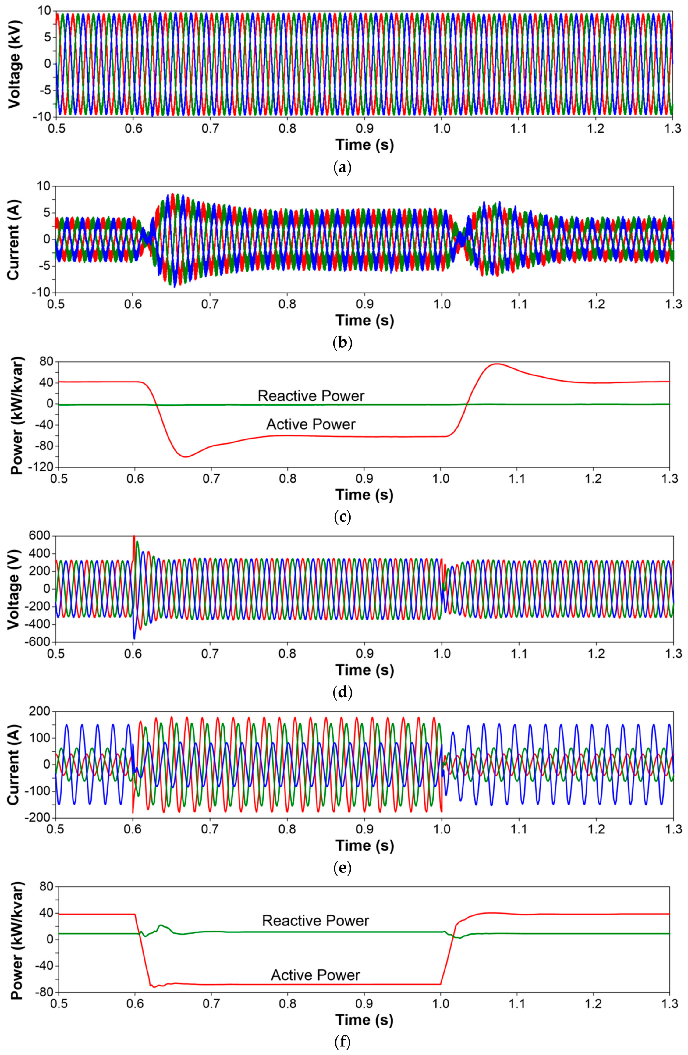
Load variation: A decrement of the load supplied from the LV terminals occurs in an initially unbalanced load. The SST behavior translates the load decrement to the active power measured at the MV terminals while the load unbalance is noticed neither before nor during nor after the load variation. Figure 8 shows that the active power variation is also detected at the MV terminals but the secondary current unbalance is not propagated to the primary currents. The voltages at the secondary side are not affected by the current unbalance, and they remain constant and balanced.
(iii)
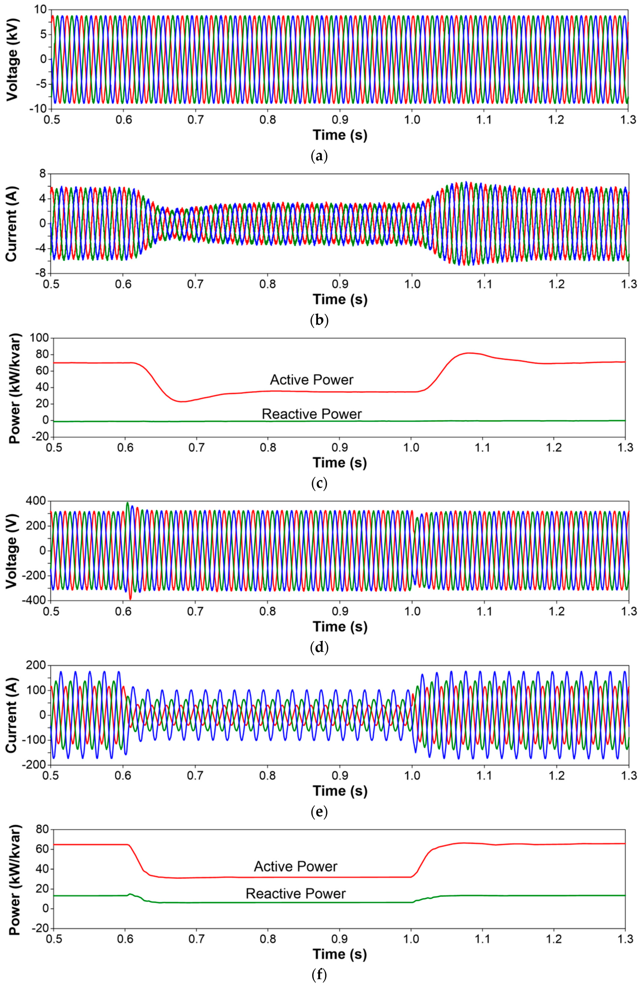
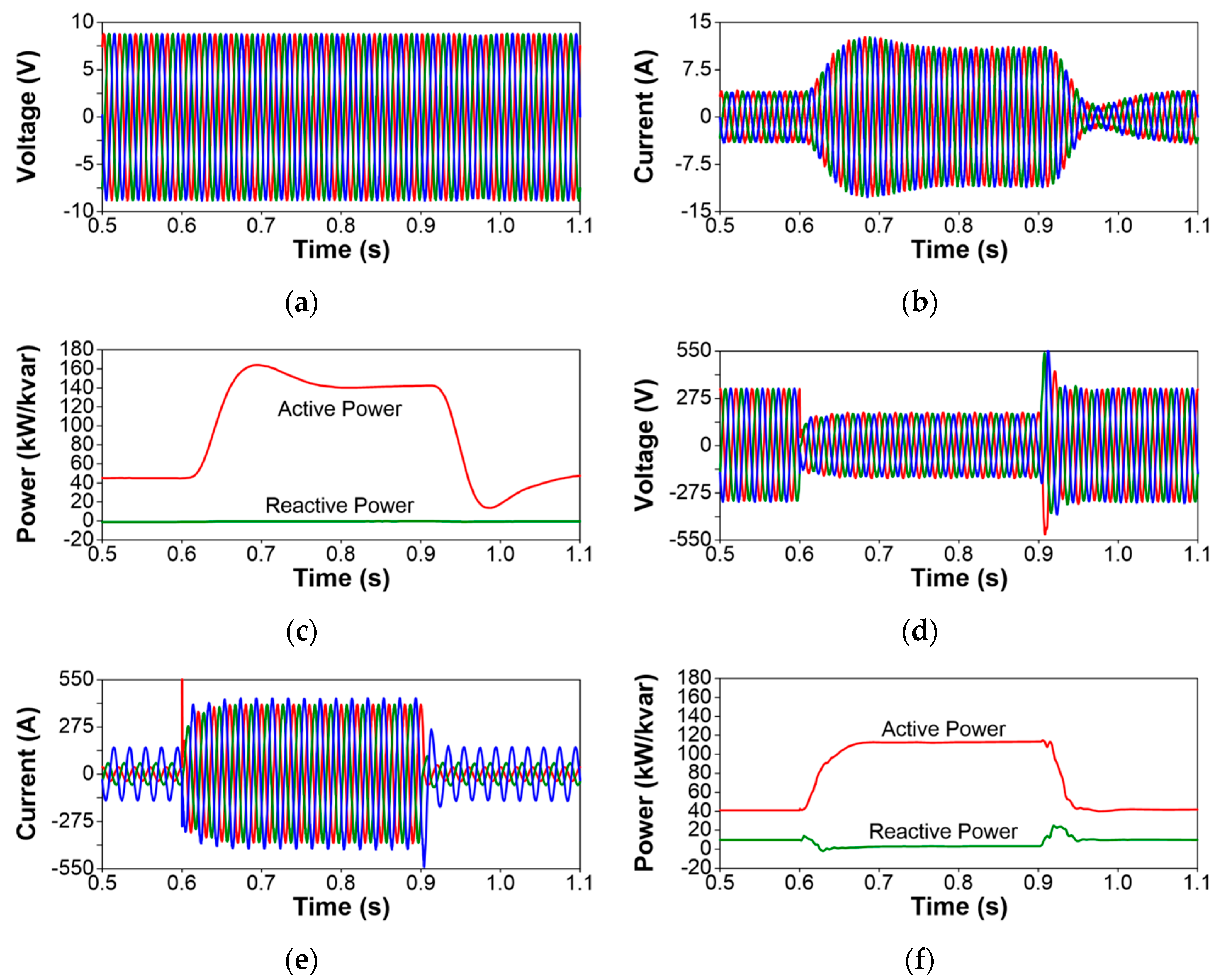
Power flow reversal: A power flow reversal is caused by the presence of both load and generation at the secondary side. As deduced from Figure 9, the load initially exceeds the generation, but during a short period this situation is reversed. Note that, as with the previous case study, the currents at the LV terminals are always unbalanced but the currents measured at the MV terminals are always balanced. This case simultaneously illustrates two of the main advantages of the SST, its capabilities to quickly control a power flow reversal between its terminals and to balance MV currents, irrespective of the situation at the LV terminals.
(iv)
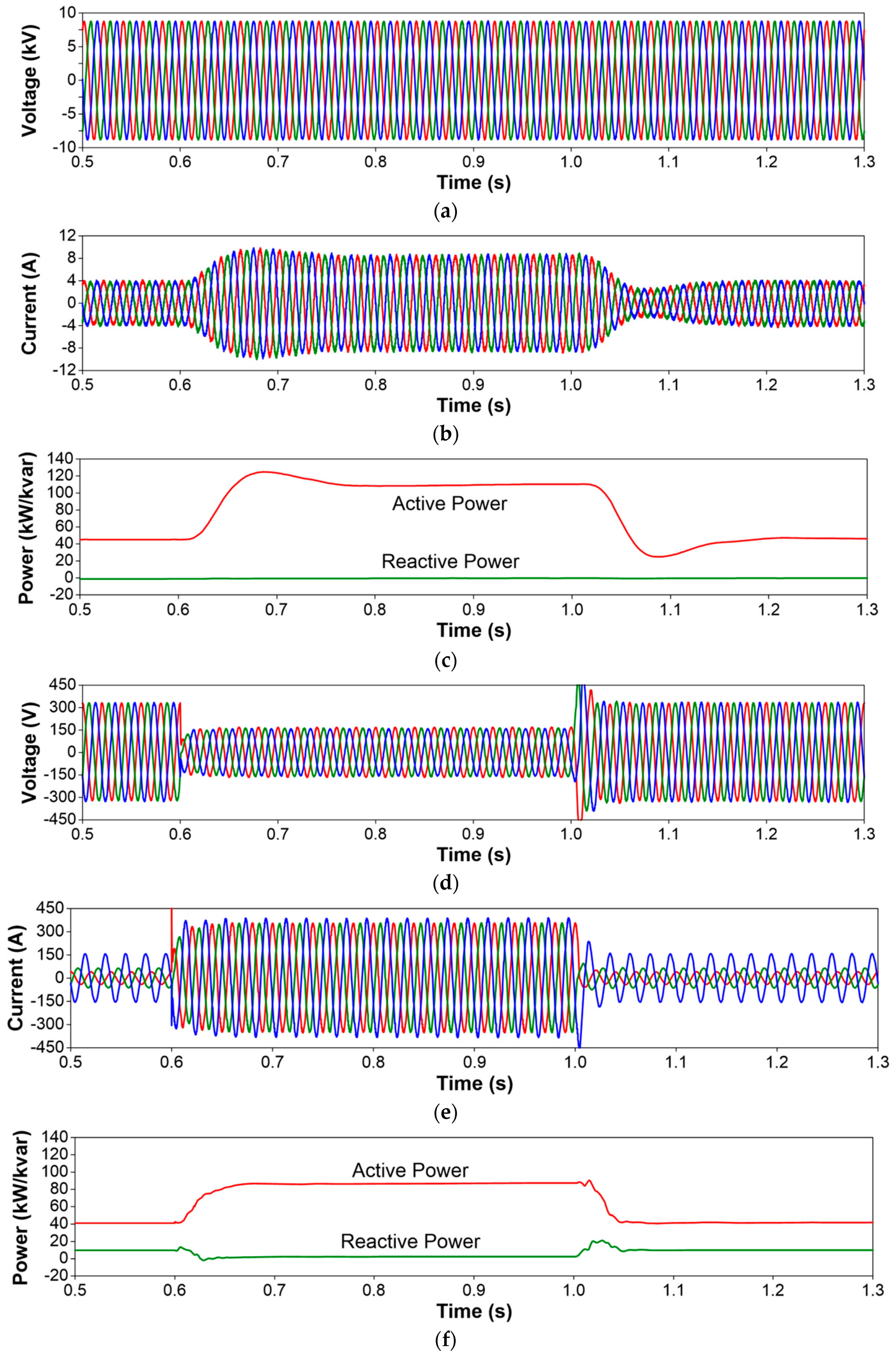
Short-circuit at the LV terminals: A bolted three-phase short-circuit occurs at the LV terminals; to avoid overcurrents that could damage the converter, the output current peak is limited to 350 A. The fault is seen from the MV side as a load increase that does not depend on the initial load level, although there can be current increase above the specified limit due to the initial current. This behavior can be understood from the analysis of waveforms shown in Figure 10. As a result of the current increase caused by the fault, secondary-side voltages decrease; consequently, the SST primary side detects a small power increase that is finally translated to an increment of the MV-side currents. With the specified current limit the maximum power measured at the MV terminals during the fault condition is close to the assumed rated power (i.e., 100 kVA); this value is only exceeded at the beginning and the end of the transient caused by the fault. Note that there can be current spikes exceeding the maximum accepted current value at the beginning and the end of the short-circuit condition.

3.3. Discussion

  • An aspect to be considered is the ride-through capabilities of the SST. Figure 7 presents the SST response in front of voltage sags and swells at the primary side. The SST can prevent the propagation of both sags and swells to the secondary side whose load will not notice the event. However, it is important to take into account that there is a limit to the sag/swell severity and duration the SST can cope with and that limit depends on the parameters selected for the power converter components and their controllers. This basically means that the SST design used in this work can provide an adequate response depending on the number of phases affected by the fault, the severity (e.g., residual voltage) and the duration of the sags/swells at the MV-side terminals. For instance, the response in front of a three-phase voltage sag with a low residual voltage and long duration (e.g., 1 s) would not be adequate and the device would not be capable of recovering the operating conditions prior to the fault once the fault conditions disappeared.
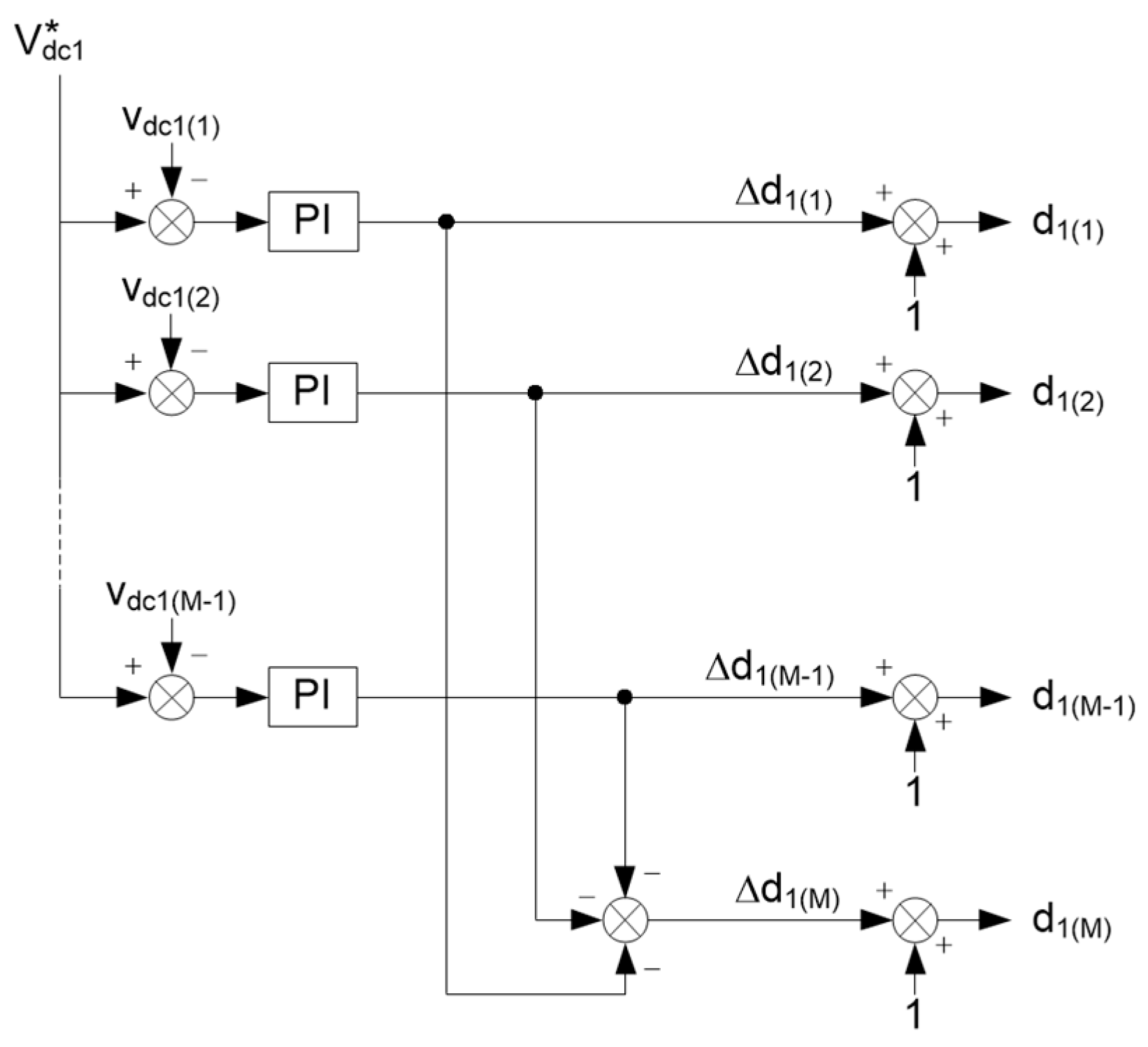
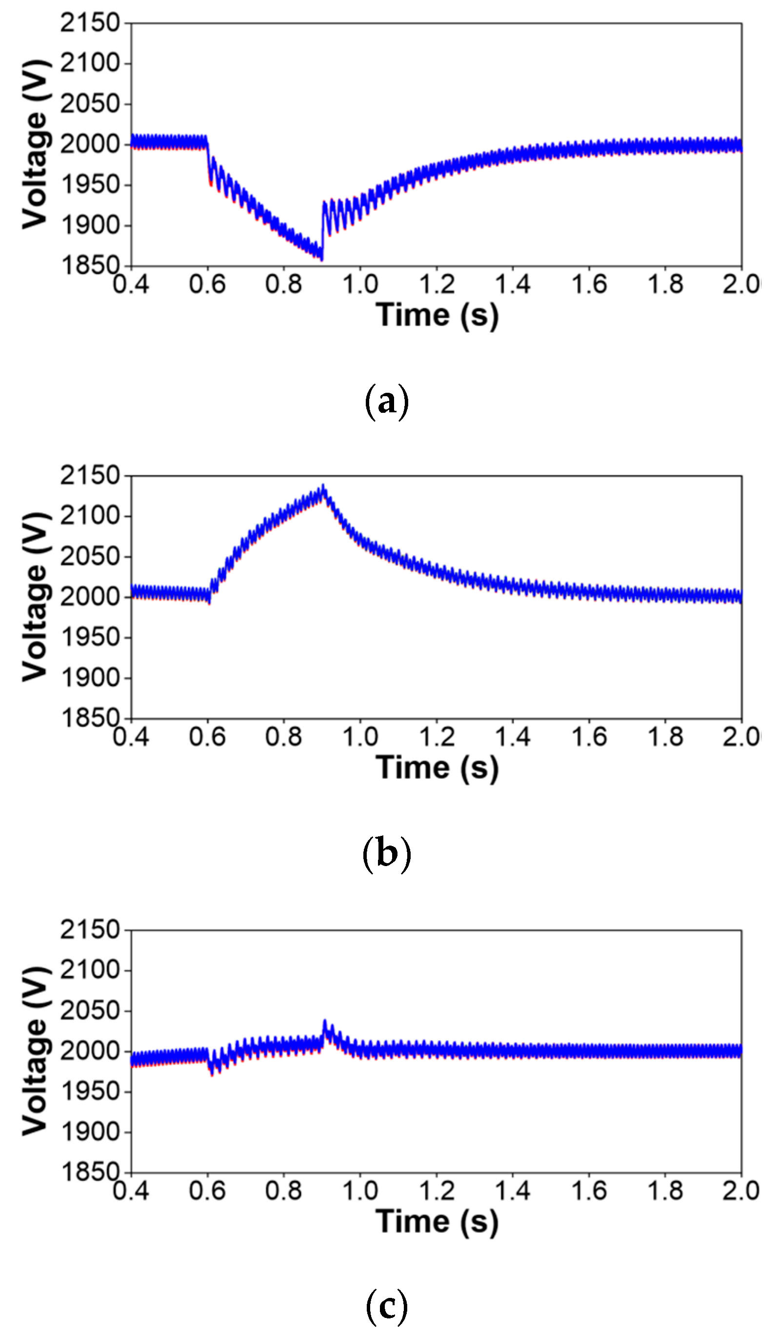
  • An important aspect of the new SST design is the requirement of a controller that could guarantee a uniform distribution of voltages in the cells that form a single-phase section of the front-end MV multilevel converter. Since the cells of a single-phase section are connected in series at the grid side and in parallel at the load side, a voltage balancing strategy in the controller of the MV side multilevel converter is required. The performance of the strategy implemented in the present model has been tested by analyzing the voltages that results at the MV dc links during the steady and transient period of two test cases analyzed above, namely the voltage sag and swell caused by a short-circuit in the test system (see Figure 7) and the power flow reversal caused by an increase of the generation connected to the LV side of the SST (see Figure 9). The target of the control of MV dc links is to keep the voltage across each MV capacitor as close as possible to 2 kV. Figure 11 and Figure 12 show the voltages across some dc links of each phase for the two case studies mentioned above. Remember that there are 6 per phase. According to these results, the deviations in all dc links with the current SST design caused before and after the transient in each case study are smaller than 8% with respect to the targeted value. On the other hand, one can observe that the response is the same in all dc links of a given phase and very similar between phases in case of flow reversal; in the case shown in Figure 11 (i.e., a voltage sag in phase A and a voltage swell in phases B and C) the response depends on the phase. This supports the choice of the controller proposed in this work to balance dc voltages and keep them within acceptable margins.
  • As illustrated with the last case study, the LV-side controller can limit the current to be supplied from the LV terminals in order to avoid large overcurrents caused by either overloads or short-circuits. Although without this limit the SST design can cope with the largest short-circuit currents and the LV-side dc link would be capable of recovering its voltage after the fault condition disappeared at the LV terminals, with this limit the effect of a short-circuit is translated to the MV terminals as an affordable overload. Actually with a limit of 350 A, the power measured at the MV terminals is above the SST rated power (i.e., 100 kVA) only during the transient that occurs at the beginning of the fault. This means that if the initial load was larger, but below 100 kVA, the impact of the selected current peak limit would cause a load decrease. Figure 13 and Figure 14 illustrate the SST behavior with other current peak limits, namely 200 and 400 A. One can observe the different response of the SST: with a limit of 200 A, the short-circuit is seen from the MV side as a load decrement (i.e., the active power is always below the SST rated power), but with a limit of 400 A the power measured at the MV side is above the SST rated power. If the current peak was not limited the active power measured at the MV side would rise to above three times the SST rated power.
  • A first approach for selecting the number of modules that should be considered for the MV side design could be based on the recommendations presented in [10]. According to this reference, there are no simple rules that could cover all applications and the semiconductor ratings have to be selected case by case. In general, power semiconductor ratings can be chosen to handle overvoltages without the need of installing expensive external overvoltage protection; in such case a security factor should be used depending on the supply power quality. Given that semiconductors with rated blocking voltages as high as 6.5 kV are currently available in the market [10], the configuration selected for this work (i.e., a six series-connected cells per phase; see Figure 1) could be practically implemented. However, a trade-off between the number of levels and the quality of the waveforms (for both currents and voltages) to be obtained will always exist; therefore, a higher number of levels could be needed for representing the SST analyzed here. As mentioned in Section 3.1, although 6 levels is a realistic choice, eight to ten levels might be also good a choice to cope with overvoltages, exhibit good quality waveforms, and use semiconductors with blocking voltages below 6.5 kV.
  • As already mentioned, the SST model analyzed in this work has been implemented in the ATP version of the EMTP. Given the complexity of the modular multilevel configuration depicted in Figure 1, the number of levels with which the model has been represented was selected as a trade-off between the simulation time for a single run and the accuracy with which results could be obtained. Although simulation results with less than 6 levels were carried out and almost negligible differences could be noticed between results with four or six levels, this last option was selected because that could represent a more realistic configuration that could be actually implemented in the lab for building a 12 kV MV side SST design. Actually, it is obvious that to obtain more accurate results rather than increasing the number of levels above six, one should consider other aspects such as the representation of semiconductor losses. Notice that without including semiconductor losses, the rated voltages assumed for any SST semiconductor is irrelevant; however, if a realistic representation of losses is desired, then the rated voltages to be selected for the semiconductors of all stages would be crucial as well as the number of levels with which the multilevel configuration of Figure 1 should be create.
  • The selection of the various parameters that have to be specified in the implemented SST model (i.e., controllers and filter parameters) was made following different approaches. In some cases, they were selected following the recommendations made by other authors. For instance, parameters of the input stage controllers were selected according to some rules provided in [24]. Other parameters, such as all those required for modelling the isolation stage and the LV-side output stage were basically those used in some previous papers by the authors; see [15,16,17]. Since the selection of some parameters was made without following any optimization procedure, a better selection remains as a future work. In any case it is worth mentioning the difficulties that are expected for some tasks. Consider, for instance, the selection of the PI controller values and filter parameters of the LV-side output converter. A flexible design of that converter should consider highly distorted LV currents due to the presence of nonlinear loads at the LV SST terminals. As with the ride-through capabilities discussed above, the present design of the output stage can cope with some harmonic distortion in the LV currents (see, for instance, simulation results presented in [15,16,17]), but above certain distortion level of the load currents the SST terminal voltage could be unacceptably distorted. A remaining task to solve these issues in the incorporation of harmonic compensation in the LV-side controllers.

4. Conclusions

This paper has presented the model of modular multilevel bidirectional SST, based on a three-stage configuration; see [13,14]. The model has been encapsulated and incorporated as a built-in capability so an ATP user only has to specify SST ratings, filter and controller parameters.
The implemented model is intended for distribution system studies in which an EMTP-like tool can be applied: it can be used in power quality studies (e.g., voltage sag propagation, current unbalance, overcurrents) and to test distribution system performance in front of many other steady-state and transient operating conditions. As supported from several references, EMTP-type tools can be used to analyze large-scale smart grids; see for instance [32,33]. Although the number of cascaded modules included in the present model for each single-phase SST branch is probably low, the performance with a higher number of modules per phase would be basically the same (except for the ripple exhibited by the primary side currents); the present representation can even be useful in the design of the SST.
The model has been tested under several dynamic and unbalanced operating conditions. Simulations results are those expected from the three-stage SST design proposed in this paper (see [15,16,17]), they confirm that intermediate capacitors provide stage decoupling and prevent disturbance at one side from propagating to the other side (e.g., secondary load immunity is achieved in front of dynamic unbalanced situations at the input side). The results have also shown that the new SST configuration incorporates the same advanced capabilities (e.g., fast voltage and power flow control, reactive power compensation, current balance) that other simplified models; see, for instance [12,15,16,17]; this supports its feasibility as a fundamental component of the future smart grid.
The ultimate goal of this work is to implement the model of a realistic SST configuration. However, it is important to remember that some aspects (e.g., semiconductor losses representation or the high-frequency transformer model) must be improved since they can have a significant influence in other studies; for instance, a more accurate representation of semiconductor losses will produce more realistic results of the SST efficiency and will also provide hints for new control strategies that could improve that efficiency. A similar conclusion can be derived from the application of a more accurate representation of the high-frequency transformer, since its behavior depends of the frequency range of voltages and currents at each side; an improved representation could provide some light about the switching frequencies and strategies that should be applied to control converters at each SST side. Future work will be addressed to obtain a more accurate representation of some SST components.
Finally, it is worth mentioning that the multilevel configuration selected for the SST model is not the only configuration proposed in the literature; see for instance [21]. Taking into account the present field experience it is too early to decide which configuration is the most adequate. In addition, it is also important to keep in mind that, according to the conclusions presented in [20], the present or similar SST designs might exceed the size, weight, and cost of an equivalent conventional-design transformer.

Author Contributions

The paper was a collaborative effort between the authors. Jacinto Martin-Arnedo was the main contributor to the implementation of the SST model. Juan A. Martinez-Velasco coordinated the work.

Conflicts of Interest

The authors declare no conflict of interest.

References

  1. Kang, M.; Enjeti, P.N.; Pitel, I.J. Analysis and design of electronic transformers for electric power distribution system. IEEE Trans. Power Electron. 1999, 14, 1133–1141. [Google Scholar] [CrossRef]
  2. Wang, D.; Mao, C.X.; Lu, J.M.; Fan, S.; Peng, F. Theory and application of distribution electronic power transformer. Electr. Power Syst. Res. 2007, 77, 219–226. [Google Scholar] [CrossRef]
  3. Fan, H.; Li, H. High-frequency transformer isolated bidirectional dc-dc converter modules with high efficiency over wide load range for 20 kVA solid-state transformer. IEEE Trans. Power Electron. 2011, 26, 3599–3608. [Google Scholar] [CrossRef]
  4. She, X.; Huang, A.Q.; Burgos, R. Review of solid-state transformer technologies and their application in power distribution systems. IEEE J. Emerg. Sel. Top. Power Electron. 2013, 1, 186–198. [Google Scholar] [CrossRef]
  5. EPRI Report Development of a New Multilevel Converter-Based Intelligent Universal Transformer: Design Analysis; EPRI: Palo Alto, CA, USA, 2004.
  6. Dommel, H.W. EMTP Theory Book; Bonneville Power Administration: Portland, OR, USA, 1986. [Google Scholar]
  7. IEC Standard Voltages, 7.0 ed.; International Electrotechnical Committee (IEC) Standard 60038; IEC: Geneva, Switzerland, 2009.
  8. Kouro, S.; Malinowski, M.; Gopakumar, K.; Pou, J.; Franquelo, L.G.; Wu, B.; Rodriguez, J.; Pérez, M.A.; Leon, J.I. Recent advances and industrial applications of multilevel converters. IEEE Trans. Ind. Electron. 2010, 57, 2553–2580. [Google Scholar] [CrossRef]
  9. Rodríguez, J.; Bernet, S.; Wu, B.; Pontt, J.O.; Kouro, S. Multilevel voltage-source-converter topologies for industrial medium-voltage drives. IEEE Trans. Ind. Electron. 2007, 54, 2930–2945. [Google Scholar] [CrossRef]
  10. Abu-Rub, H.; Holtz, J.; Rodriguez, J.; Baoming, G. Medium-voltage multilevel converters-State of the art, challenges, and requirements in industrial applications. IEEE Trans. Ind. Electron. 2010, 57, 2581–2596. [Google Scholar] [CrossRef]
  11. Backlund, B.; Carroll, E. Voltage Ratings of High Power Semiconductors; ABB Semiconductors: Lenzburg, Switzerland, 2006. [Google Scholar]
  12. González, F.; Martin-Arnedo, J.; Alepuz, S.; Martinez, J.A. EMTP model of a bidirectional multilevel solid state transformer for distribution system studies. In Proceedings of the IEEE PES General Meeting, Denver, CO, USA, 26–30 July 2015. [Google Scholar]
  13. Zhao, T.; Wang, G.; Bhattacharya, S.; Huang, A.Q. Voltage and power balance control for a cascaded H-bridge converter-based solid-state transformer. IEEE Trans. Power Electron. 2013, 28, 1523–1532. [Google Scholar] [CrossRef]
  14. She, X.; Huang, A.Q.; Ni, X. A cost effective power sharing strategy for a cascaded multilevel converter based solid state transformer. In Proceedings of the IEEE Energy Conversion Congress Exposition (ECCE), Denver, CO, USA, 15–19 September 2013. [Google Scholar]
  15. Alepuz, S.; González, F.; Martin-Arnedo, J.; Martinez, J.A. Solid state transformer with low-voltage ride-through and current unbalance management capabilities. In Proceedings of the 39th Annual Conference IEEE Industrial Electronics Society (IECON), Vienna, Austria, 10–13 November 2013. [Google Scholar]
  16. Alepuz, S.; González-Molina, F.; Martin-Arnedo, J.; Martinez-Velasco, J.A. Development and testing of a bidirectional distribution electronic power transformer model. Electr. Power Syst. Res. 2014, 107, 230–239. [Google Scholar] [CrossRef]
  17. Martinez-Velasco, J.A.; Alepuz, S.; González-Molina, F.; Martin-Arnedo, J. Dynamic average modeling of a bidirectional solid state transformer for feasibility studies and real-time implementation. Electr. Power Syst. Res. 2014, 117, 143–153. [Google Scholar] [CrossRef]
  18. She, X.; Yu, X.; Wang, F.; Huang, A.Q. Design and demonstration of a 3.6-kV–120-V/10-kVA solid-state transformer for smart grid application. IEEE Trans. Power Electron. 2014, 29, 3982–3996. [Google Scholar] [CrossRef]
  19. Huber, J.E.; Kolar, J.W. Common-mode currents in multi-cell solid-state transformers. In Proceedings of the 2014 International Power Electronics Conference, Hiroshima, Japan, 18–21 May 2014. [Google Scholar]
  20. Huber, J.E.; Kolar, J.W. Volume/weight/cost comparison of a 1 MVA 10 kV/400 V solid-state against a conventional low-frequency distribution transformer. In Proceedings of the IEEE Energy Conversion Congress Exposition (ECCE), Pittsburgh, PA, USA, 14–18 November 2014. [Google Scholar]
  21. Garcia Montoya, R.J.; Mallela, A.; Balda, J.C. An evaluation of selected solid-state transformer topologies for electric distribution systems. In Proceedings of the IEEE Applied Power Electronics Conference Exposition (APEC), Charlotte, NC, USA, 15–19 March 2015. [Google Scholar]
  22. Kim, D.; Lee, D. Inverter output voltage control of three-phase UPS systems using feedback linearization. In Proceedings of the 33rd Annual Conference IEEE Industrial Electronics Society (IECON), Taipei, Taiwan, 5–8 November 2007. [Google Scholar]
  23. Dai, J.; Xu, D.; Wu, B. A novel control scheme for current-source-converter-based PMSG wind energy conversion systems. IEEE Trans. Power Electron. 2009, 24, 963–972. [Google Scholar]
  24. Lee, D.; Jang, J. Output voltage control of PWM inverters for stand-alone wind power generation systems using feedback linearization. In Proceedings of the 14th Industry Applications Society Annual Meeting, Hong Kong, China, 2–6 October 2005. [Google Scholar]
  25. De Doncker, R.W.; Divan, D.M.; Kheraluwala, M.H. A three-phase soft-switched high-power-density dc-dc converter for high power applications. IEEE Trans. Ind. Appl. 1991, 27, 63–73. [Google Scholar] [CrossRef]
  26. Perales, M.A.; Prats, M.M.; Portillo, R.; Mora, J.L.; Leon, J.I.; Franquelo, L.G. Three-dimensional space vector modulation in abc coordinates for four-leg voltage source converters. IEEE Power Electron. Lett. 2003, 99, 104–109. [Google Scholar] [CrossRef]
  27. Zhang, R.; Prasad, V.H.; Boroyevich, D.; Lee, F.C. Three-dimensional space vector modulation for four-leg voltage-source converters. IEEE Trans. Power Electron. 2002, 17, 314–326. [Google Scholar] [CrossRef]
  28. Vechiu, I.; Curea, O.; Camblong, H. Transient operation of a four-leg inverter for autonomous applications with unbalanced load. IEEE Trans. Power Electron. 2010, 25, 399–407. [Google Scholar] [CrossRef]
  29. Ebrahimzadeh, E.; Farhangi, S.; Iman-Eini, H.; Blaabjerg, F. Modulation technique for four-leg voltage source inverter without a look-up table. IET Power Electron. 2016, 9, 648–656. [Google Scholar] [CrossRef]
  30. Gole, A.M.; Keri, A.; Nwankpa, C.; Gunther, E.W.; Dommel, H.W.; Hassan, I.; Marti, J.R.; Martinez, J.A.; Fehrle, K.G.; Tang, L.; et al. Guidelines for modeling power electronics in electric power engineering applications. IEEE Trans. Power Deliv. 1997, 12, 505–514. [Google Scholar] [CrossRef]
  31. Sen, K.K.; Sen, M.L. Introduction to FACTS Controller: Theory, Modeling, and Applications; IEEE Press and John Wiley: Hoboken, NJ, USA, 2009. [Google Scholar]
  32. Spitsa, V.; Salcedo, R.; Ran, X.; Martinez, J.; Uosef, R.; de León, F.; Czarkowski, D.; Zabar, Z. Three-phase time-domain simulation of very large distribution networks. IEEE Trans. Power Deliv. 2012, 27, 677–687. [Google Scholar] [CrossRef]
  33. De Leon, F.; Salcedo, R.; Ran, X.; Martinez-Velasco, J.A. Time-Domain Analysis of the Smart Grid Technologies: Possibilities and Challenges. In Transient Analysis of Power Systems: Solution Techniques, Tools and Applications; Martinez-Velasco, J.A., Ed.; John Wiley & Sons, Inc.: Hoboken, NJ, USA, 2015. [Google Scholar]
Figure 1. Cascaded modular bidirectional SST implementation: (a) Converter cell (with input H-bridge converter and dc-dc converter); (b) Modular design of a single-phase cell (back-to-back converter); (c) Overall SST configuration.
Energies 10 00521 g001
Figure 2. Medium-voltage side control.
Energies 10 00521 g002
Figure 3. DC voltage balance controller.
Energies 10 00521 g003
Figure 4. Isolation stage control.
Energies 10 00521 g004
Figure 5. Low-voltage side control.
Energies 10 00521 g005
Figure 6. Diagram of the test system.
Energies 10 00521 g006
Figure 7. Simulation results: Voltage sag and swells at the primary side. (a) Primary SST terminal voltages—MV level; (b) Primary SST terminal currents—MV level; (c) Primary SST terminal power—MV level; (d) Secondary SST terminal voltages—LV level; (e) Secondary SST terminal currents—LV level; (f) Secondary SST terminal power—LV level.
Energies 10 00521 g007
Figure 8. Simulation results: Load variation with an initial load unbalance. (a) Primary SST terminal voltages—MV level; (b) Primary SST terminal currents—MV level; (c) Primary SST terminal power—MV level; (d) Secondary SST terminal voltages—LV level; (e) Secondary SST terminal currents—LV level; (f) Secondary SST terminal power—LV level.
Energies 10 00521 g008
Figure 9. Simulation results: Power flow reversal. (a) Primary SST terminal voltages—MV level; (b) Primary SST terminal currents—MV level; (c) Primary SST terminal power—MV level; (d) Secondary SST terminal voltages—LV level; (e) Secondary SST terminal currents—LV level; (f) Secondary SST terminal power—LV level.
Energies 10 00521 g009
Figure 10. Simulation results: Three-phase short-circuit at the secondary LV terminals. (a) Primary SST terminal voltages—MV level; (b) Primary SST terminal currents—MV level; (c) Primary SST terminal power—MV level; (d) Secondary SST terminal voltages—LV level; (e) Secondary SST terminal currents—LV level; (f) Secondary SST terminal power—LV level.
Energies 10 00521 g010
Figure 11. Simulation results: Voltage sag and swell at the primary side. MV-side dc link voltages. (a) Phase A cells; (b) Phase B cells; (c) Phase C cells.
Energies 10 00521 g011
Figure 12. Simulation results: Power flow reversal. MV-side dc link voltages. (a) Phase A cells; (b) Phase B cells; (c) Phase C cells.
Energies 10 00521 g012
Figure 13. Simulation results: Three-phase short-circuit at the LV terminals (Limit = 200 A). (a) Primary SST terminal voltages—MV level; (b) Primary SST terminal currents—MV level; (c) Primary SST terminal power—MV level; (d) Secondary SST terminal voltages—LV level; (e) Secondary SST terminal currents—LV level; (f) Secondary SST terminal power—LV level.
Energies 10 00521 g013
Figure 14. Simulation results: Three-phase short-circuit at the LV terminals (Limit = 400 A). (a) Primary SST terminal voltages—MV level; (b) Primary SST terminal currents—MV level; (c) Primary SST terminal power—MV level; (d) Secondary SST terminal voltages—LV level; (e) Secondary SST terminal currents—LV level; (f) Secondary SST terminal power—LV level.
Energies 10 00521 g014
Table 1. SST Main Parameters.
ParameterValue
Primary side filter resistance (R1)0.5 Ω
Primary side filter inductance (L1)10 mH
MV DC link capacitance (Cdc1)500 µF
LV DC link capacitance (Cdc2)3000 µF
Secondary side filter resistance (R2)0.1 Ω
Secondary side filter inductance (L2)2 mH
Secondary side filter capacitance (C2)470 µF
Neutral resistance (Rn)0.1 Ω
Neutral inductance (Ln)1 mH
Rectifier/Inverter switching frequency10 kHz
Transformer operating frequency2 kHz
Transformer short-circuit resistance (Rt)0.1 Ω
Transformer leakage inductance (Lt)1 mH

