
Design and Evaluation of an Efficient Three-Phase Four-Leg Voltage Source Inverter with Reduced IGBTs


1
Shenzhen Research Institute, City University of Hong Kong, Nanshan District, Shenzhen 518057, China
2
School of Energy and Environment, City University of Hong Kong, 83 Tat Chee Avenue, Kowloon Tong, Hong Kong, China
3
Research Laboratory of Electronics, Massachusetts Institute of Technology, Cambridge, MA 02139, USA
*
Author to whom correspondence should be addressed.
Energies 2017, 10(4), 530; https://doi.org/10.3390/en10040530
Submission received: 4 January 2017
/
Revised: 3 April 2017
/
Accepted: 10 April 2017
/
Published: 13 April 2017
(This article belongs to the Special Issue Power Electronics and Power Quality)
Abstract
:This paper presents a new three-phase four-leg voltage source inverter (VSI), which achieves a high cost effectiveness for mega-watt level system applications. The proposed four-leg inverter adopts the integrated topology with thyristors and insulated-gate bipolar transistors (IGBTs), which aims to reduce the number of IGBTs. In order to handle the zero sequence current, a neutral leg via incorporating IGBTs is artfully integrated with the regular phase legs. Furthermore, the modelling principles are elaborated and analyzed, which emphasizes switching states and voltage vectors in six segments based on the states of thyristors. Finally, by using the carrier-based pulse width modulation (PWM) method, the closed-loop current control of the proposed inverter is verified by both simulation and experimentation.
1. Introduction
Three-phase voltage source inverters (VSI) are widely used in industrial applications such as uninterruptable power supply (UPS) [1,2], motor drives [3,4,5], wireless power transfer [6] and distributed power generation system [7,8]. Unfortunately, this conventional topology is hard to keep the neutral point potential in a constant level under unbalanced load conditions, which leads to asymmetric output voltage [9]. To solve this problem, a split capacitor three-phase inverter is investigated in [10], but such a topology poses a problem of low DC voltage utilization. Alternatively, the three-phase four-leg VSI that connects the neutral point to the fourth leg is investigated by [11,12,13,14,15,16,17,18]. In fact, three-phase four-leg VSI is widely used in various industrial applications, such as distributed power generation, three phase UPS systems and series active filters, where the balanced three-phase voltage output is required during unbalanced load conditions [19,20,21]. However, the topology and control algorithm of the four-leg VSI are inherently more complex than the traditional three-phase type.
There has been a substantial increasing trend in control strategy investigations on three-phase four-leg inverters, including the carrier-based pulse width modulation (PWM) [22,23], space vector modulation algorithm [24,25], and digital predictive control [26,27]. Firstly, a minimally switched control algorithm is studied, which can minimize switching operations and monitor the current polarity for three-phase four-leg inverter [28]. Then, a selective harmonic elimination (SHE) control strategy on a three-phase four-leg inverter is reported in [29], where the lower order nontriplen harmonics are eliminated by using Fourier-based equations on line-to-line basis as conventional SHE technology to express the control signals of three legs. In addition, two methods that mitigate the load neutral point voltage (LNPV) for three-phase four-leg inverters are analyzed, which are based on the PWM strategy and the common mode filter, respectively [30]. Moreover, a decoupled sequence control strategy, employing positive sequence, negative sequence, and zero sequence controllers is studied in [31].
However, the available publications on three-phase four-leg inverters are limited to eight-insulated-gate bipolar transistors (IGBTs) topologies, as illustrated in Figure 1a. In mega-watt level applications, the IGBT with a rated current of thousands of ampere is not cost-effective and is not suitable for some cost-sensitive situations.
The purpose of this paper is to propose and evaluate an IGBT-reduced three-phase four-leg VSI that possesses the attractive feature of four-leg inverters. The proposed topology can reduce cost significantly, especially for mega-watt level applications such as electric ship propulsion systems, microgrid converters, motor drives, and so on. In Section 2, the configuration of the proposed inverter and the operation principle will be introduced. Section 3 will be devoted to deducing the representation of inverter output voltages as a three-dimensional space vector in a stator oriented αβγ rectangular coordinate. In Section 4, closed-loop current control strategy of the proposed inverter will be presented. Then, simulation and experiment results will be given to verify the validity of the proposed inverter in Section 5. Consequently, a quantitative comparison between the proposed inverter and the conventional three-phase four-leg inverter will be made in Section 6. Finally, conclusions will be drawn in Section 7.
2. Topology and Operation Principle of the Proposed Inverter
The proposed cost-effective three-phase four-leg VSI is shown in Figure 1b. In particular, the proposed inverter has the definite benefit of the reduction of three IGBTs. In addition, according to the current market price, with a rated current of one thousand ampere, the thyristor is much cheaper than the IGBT. Though the number of gating signals and control complexity increase inherently due to the existence of the fourth leg, it possesses the advantage of handling unbalanced loads over the three-leg inverter.
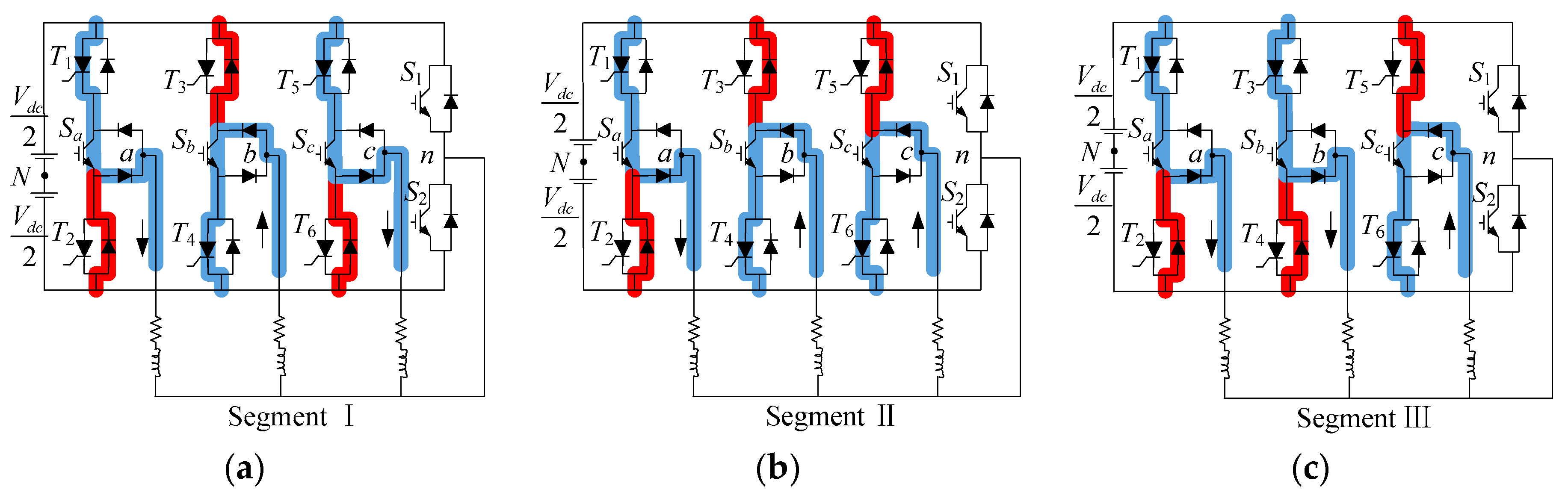
From Figure 1b, it also can be found that the thyristors are employed in phase legs, while the IGBTs and diodes are in the fourth leg. Upon the commutation of the phase current alone, the thyristors turn off naturally. Thus, the zero-crossing point of phase currents is the major factor which determines the switching time of thyristors. Also, it is worth mentioning that the directions of injected currents for the analysis of the converter operation modes are shown in Figure 1b. Normally, the thyristors in the same leg are not allowed to be switched on or off simultaneously. In particular, the upper one is switched on during the positive cycle, while the lower one is on during the negative cycle. Consequently, there are six combinations for upper thyristor switching states and each combination corresponds to a specific time interval, as shown in Figure 2.
In Segment I, T1 is switched on, T3 is off and T5 is on. For phase a, when Sa is turned on, current flows through T1, Sa, and VD3. When Sa is turned off, the freewheeling current flows through VD4, as shown in Figure 3a. It should be noted the current direction in phase b is negative in Segment I. Thus, the current flows through VD6, Sb, and T4 when Sb is on, and the current passes through the freewheeling diode VD5 when Sb is off. Meanwhile, phase c is in the same condition as phase a, while the fourth leg can be analyzed as a typical inverter leg. According to these situations, the thyristor-IGBT combined leg can be regarded as the same flowing path as a typical inverter leg. Therefore, based on the proposed topology, one IGBT can provide the flowing path for both positive and negative currents, whereas the current needs to pass through two different IGBTs in the conventional inverter leg.
The current flow paths for the other five segments can be analyzed in the same manner, while all individual paths are illustrated in Figure 3b–f.
3. Mathematical Modelling
It should be noted that when the thyristors are involved, the voltage equations would differ from those produced by the conventional three-phase four-leg inverter. Referring to the middle point of the direct current (DC) link, the voltages in each leg are defined separately for the positive and negative cycles of the alternating current (AC) which is based on consideration of the thyristor states. The relationship can be described as,
where vaN, vbN, vcN, and vnN are the voltage potentials between points a, b, c, n and N, respectively.
Referring to Figure 1b, the phase voltage that is represented in the matrix can be governed by
where van, vbn, and vcn are the voltage potentials between points a, b, c, and n, respectively.
Normally, a four-leg inverter consists of 24 = 16 possible switching states, while for the new topology, the states of thyristors have to be considered beside the states of IGBTs. The relationship between phase voltage and switching states of phase a are summarized in Table 1, where the UT stands for “Upper Thyristor”. Based on the same rationale, the phase voltages of phase b and phase c can be analyzed in the same manner.
It can be seen that there are, in total, eight switching-state combinations in accordance to three voltages for each phase. When the states of UT are opposite, the corresponding phase voltage is inverse. This feature can be utilized to simplify the control algorithm of the proposed inverter. The typical converter’s modes of voltage vectors are analyzed in the aforementioned six segments, also known as intervals, individually.
Since the state of the thyristor does not change within one segment, the voltage vectors can only be defined according to the IGBT state in each segment. Therefore, the basic voltage vectors of 16-switching states are expressed in a binary system as 0000, 0001, …, 1111, respectively, where the switching states are described in the order of Sa, Sb, Sc, and S1. The distributions of the voltage vectors in all six segments can be obtained via Equations (1)–(4). The corresponding results are summarized in Table 2.
The phase voltages can also be expressed regarding the load and current as
where
Moreover, (5) in αβγ coordinate can be further formulated as
where
In particular, the quantities van, vbn, vcn and ia, ib, ic in Equation (5) can be transformed to αβγ coordinate.
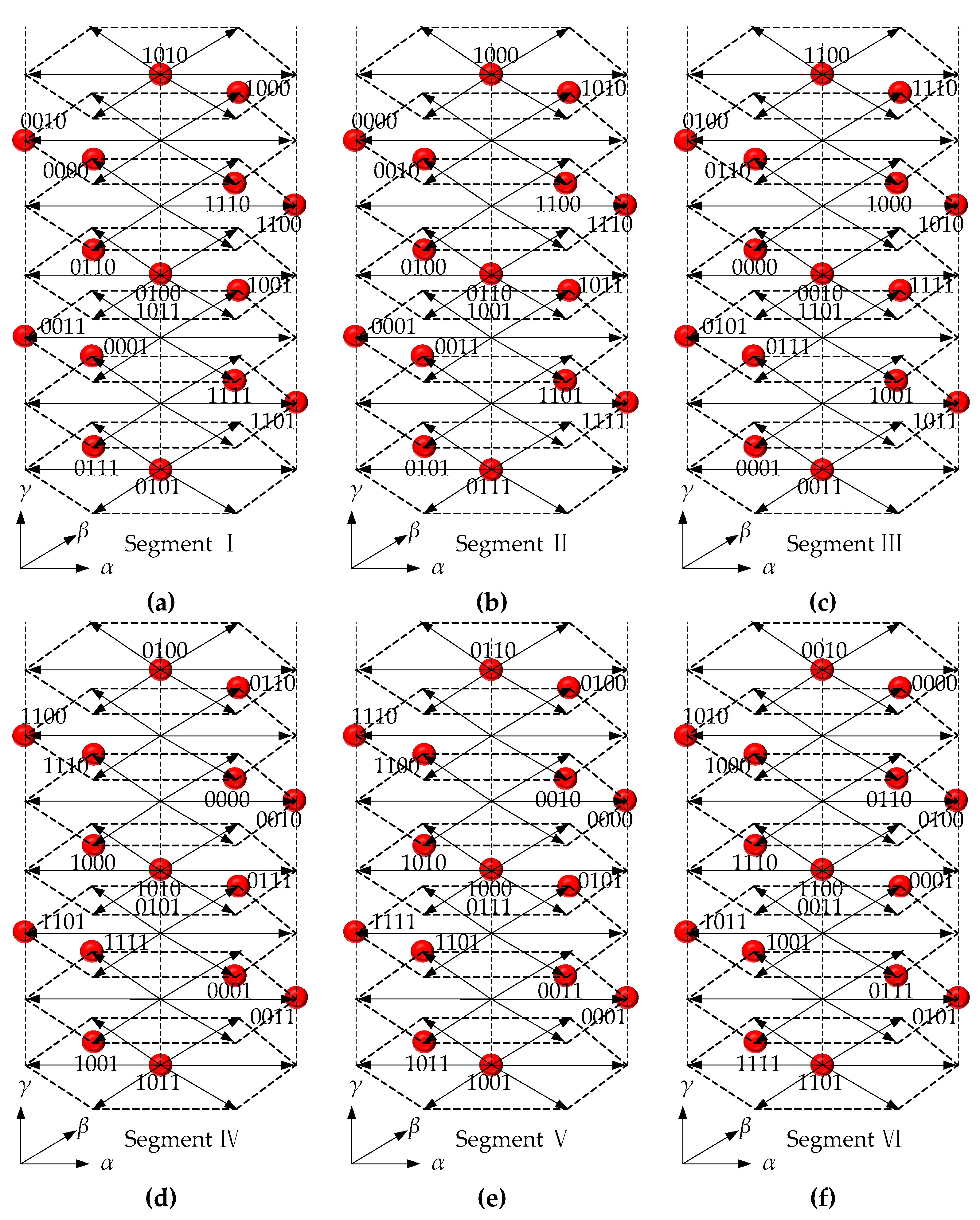
Through (1)–(8), the voltage vectors vα, vβ and vγ in αβγ coordinate can be obtained from Segment I to Segment VI, respectively. vα and vβ form a hexagon in the αβ plane as shown in Figure 4, where each vector corresponds to a combination of different switching states in different segments. Moreover, it should be noted that vγ is determined by the state of the fourth leg. The graphical representation of all voltage vectors in the six segments in αβγ coordinate is shown in Figure 5. It can be seen that there are fourteen nonzero voltage vectors and two zero vectors in each segment. However, the same voltage vector in different segments is formed by different corresponding switching state combinations. For instance, 0110 in Segment I forms the same voltage vector as 0100 in Segment II. Moreover, there are seven αβ planes in each coordinate. The distance between each of them is 1/3.
4. Current Control Algorithm for Proposed Inverter
Carrier-based pulse width modulation (PWM) with proportional resonant (PR) controllers and a pulse computational module (PCM) are employed to regulate the output currents of the proposed inverter. The control algorithm is depicted in Figure 6.
The PR regulator is used due to its capability of tracking the AC current with zero steady-state error. The practical PR controller is described by the transfer function [32]:
where kp is the proportional gain, Ti is the integral gain, ωr is the resonant cut off frequency, and ω0 is equal to the inverter frequency.
The error between the measured current and the reference are sent to the PR controller to produce commands var, vbr and vcr. It is worth mentioning that the neutral leg is commanded by the average of the other three phase voltages,
Each modulator generates a signal for one inverter leg when keeping with the principle of PWM. However, except for the neutral leg, the signals produced by PWM modulator have to be processed through a PCM before sending them to IGBTs. According to Table 1, it indicates that the opposite state thyristor corresponds to the inverse phase voltage. Therefore, the switching signal values generated from the PWM modulator for phase legs in the negative cycle should be flipped using a “NOT” function. This computation process can be expressed through the piecewise functions where, the pulse computation function for the positive cycle of phase a is shown as:
the pulse computation function for the negative cycle of phase a is shown as:
the pulse computation function for the positive cycle of phase b is shown as:
the pulse computation function for the negative cycle of phase b is shown as:
the pulse computation function for the positive cycle of phase c is shown as:
the pulse computation function for the negative cycle of phase c is shown as:
here, T is the period of the phase current.
Using the PCM, all IGBTs are controlled. Phase shift factor ∆t is defined in piecewise functions. The optimum value of ∆t is tuned to reduce the total harmonics distortion (THD) of the output current. To control the thyristors, a triggering pulse is sent to the upper thyristor at the start of each positive cycle and to the lower thyristor at the start of each negative cycle. When the current crosses zero, the thyristor is switched off accordingly.
5. Verification Results of Proposed Topology
In order to verify the proposed topology, simulations and experiments are conducted and analyzed. The system parameters for the simulation are listed in Table 3. The closed-loop current feedback control was implemented.
5.1. Simulation Results
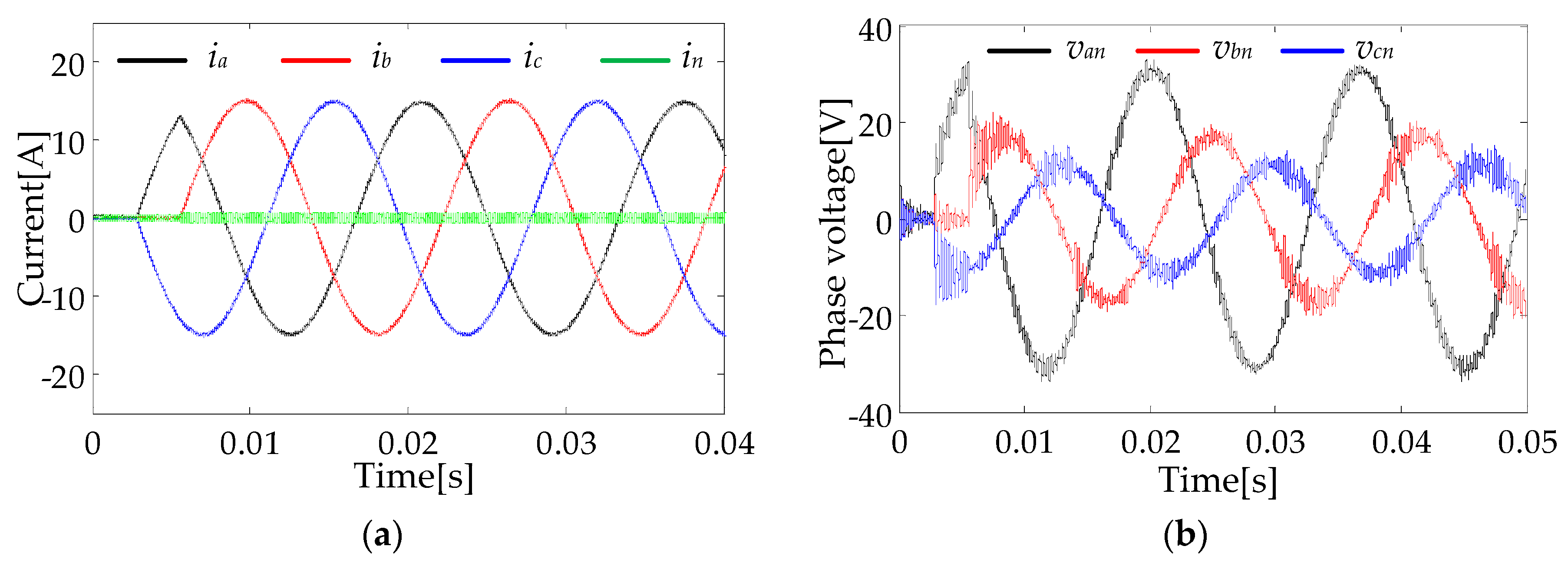
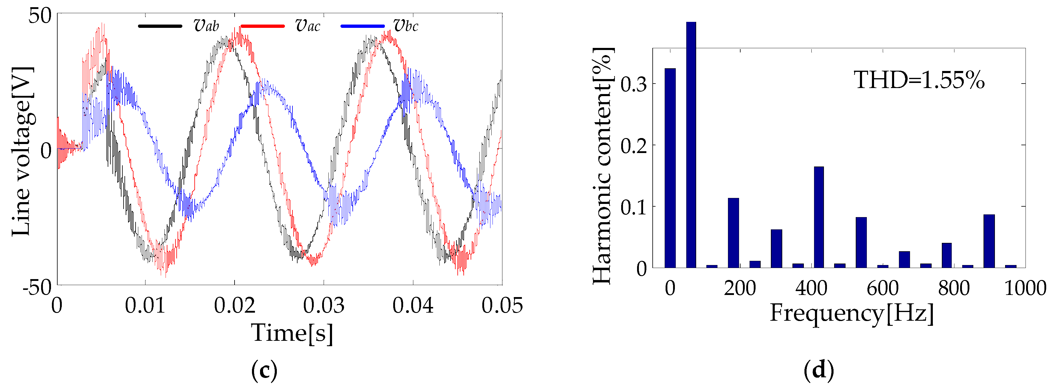
Using the current feedback PWM scheme, the proposed inverter is operated with a balanced load, as shown in Figure 7. With the support of the PR controller loop, the static performance of the current is satisfactory. Moreover, the output current and phase voltage are well-balanced. Subsequently, the unbalanced load condition is investigated with the load resistors of 2 Ω, 1 Ω and 0.5 Ω, respectively. As shown in Figure 8a, the output currents stay balanced regardless of the unbalanced loads. In the meantime, the line to line voltages in balanced and unbalanced load conditions are shown in Figure 7c and Figure 8c, respectively. It can be observed that under the unbalanced loads, the current THD is slightly increased, from 1.45% to 1.55%. Furthermore, when the inverter is operated as the controlled current source, the appropriate adjustments of the output voltages are shown in Figure 8b. In this way, the amplitudes of the output currents are kept constant under unbalanced loads.
5.2. Experimental Results
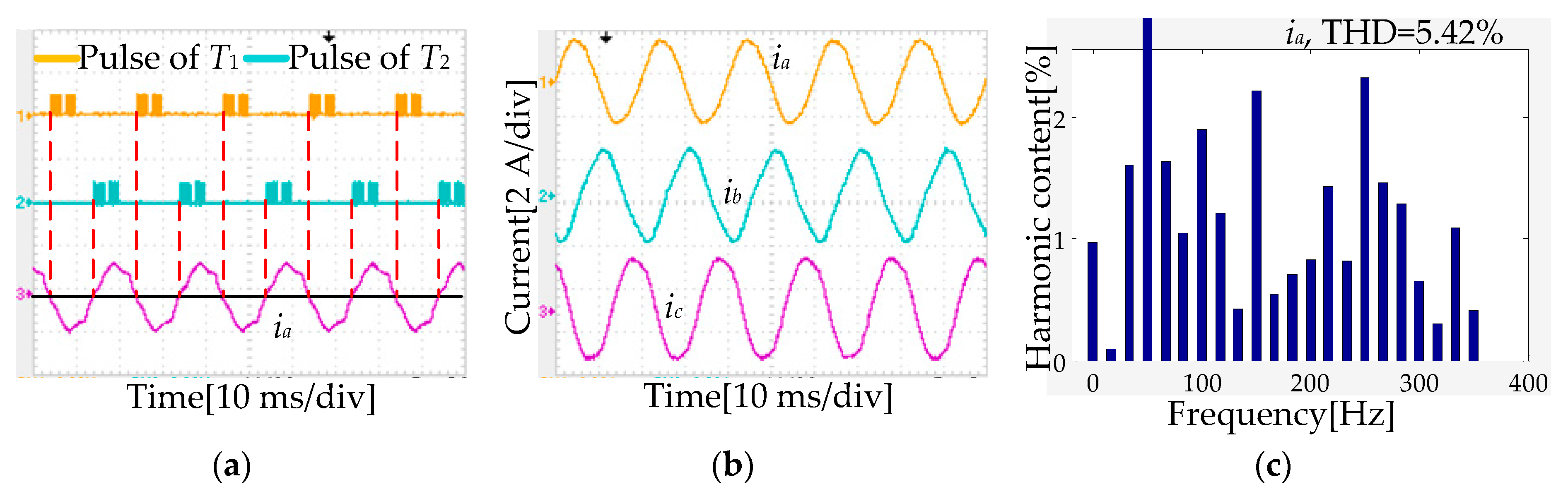
To further verify the performance of the proposed converter, a prototype of the new converter is built as shown in Figure 9. The experimental setup mainly includes the inverter prototype, drive circuit for IGBTs, drive circuit for thyristors, current sensors, R-L load, DC power supply and a dSPACE 1104 controller. The load parameters are: R = 5 Ω, 4 Ω, 3 Ω and L = 5 mH.
The validity of the improved PWM-PR controller current control algorithm for the proposed three-phase four-leg converter is investigated. It can be observed from Figure 10a that the triggering pulse for the upper thyristor is generated when the current crosses zero from negative to positive, while the triggering pulse for the lower thyristor is generated when the current crosses zero from positive to negative. Figure 10b,c shows the phase current waveforms and THD of the proposed converter at a steady 2 A reference current with an unbalanced load. By importing the data from oscilloscope into Matlab, the THD of phase a current is obtained as 5.42%.
Therefore, the characteristics of the proposed three-phase four-leg converter are verified by simulation and experimentation. It proves that the proposed cost-effective converter possesses a distinct merit for potential implementation in high power applications, such as electric ship propulsion systems, microgrid converters, motor drives, and so on.
6. Comparison
To further demonstrate the merit of the proposed three-phase four-leg inverter, a quantitative comparison with the conventional eight-IGBTs VSI is conducted and discussed. For a fair comparison, the converter ratings are unified as the power level of 2.88 MW, whereas the DC voltage and current are set to 1600 V and 1800 A. The specifications of IGBT, thyristor, and diode can be tabulated in Table 4.
First, the number of switches for the proposed converter and the conventional three-phase four-leg inverter can be determined according to Figure 1. The numbers of single switch IGBT module, dual switch IGBT module, thyristor and diode for the proposed converter and conventional converter are 0, 4, 0, 0 and 1, 1, 6, 12, respectively. Subsequently, size and cost comparison can be calculated. The size and weight are first compared with the specific data. Then, their cost is quantitatively compared and discussed.
The estimated data of the proposed and conventional inverters, namely, the size, weight and cost are summarized in Table 5. It can be observed that the proposed inverter has a definite advantage in terms of lower cost, although it suffers from its relatively complicated structure and larger size. Approximately USD 1094 can be saved by one three-phase four-leg inverter for the power level of a 2.88 MW system, which is appreciated for the demand side. Therefore, the proposed inverter has great potential for mega-watt level cost-sensitive applications.
7. Conclusions
In this paper, a new integrated IGBT-thyristor three-phase four-leg VSI is proposed, analyzed and evaluated, specifically for mega-watt level applications. As compared with traditional four-leg inverters, the proposed inverter achieves a distinct advantage of higher cost-effectiveness. The operation principle of the proposed inverter is investigated and discussed. The inverter output voltage in αβγ coordinate of each segment is also presented. Moreover, the current control strategy based on carrier-based PWM with PR controllers and the PCM is developed and analyzed. Demonstration results of simulation and experimentation for closed-loop current control are accomplished, which verifies the functionality of the proposed inverter under balanced and unbalanced load conditions.
Acknowledgments
The work described in this paper was supported by a grant (Project No. 51677159) from the Natural Science Foundation of China (NSFC), China.
Author Contributions
The work presented in this paper is the output of research projects undertaken by Chunhua Liu. In specific, Yixiao Luo and Chunhua Liu developed the topic, designed the system, analyzed the results, and wrote this paper. Feng Yu and Christopher H.T. Lee helped review and improve the paper.
Conflicts of Interest
The authors declare no conflict of interest.
References
- Kim, E.-K.; Mwasilu, F.; Choi, H.H.; Jung, J.-W. An observer-based optimal voltage control scheme for three-phase UPS systems. IEEE Trans. Ind. Electron. 2015, 62, 2073–2081. [Google Scholar] [CrossRef]
- Hossain, R.; Lipo, T.; Kwon, B. A novel topology for a voltage source inverter with reduced transistor count and utilizing naturally commutated thyristors with simple commutation. In Proceedings of the 2014 International Symposium on Power Electronics Electrical Drives Automation and Motion (SPEEDAM), Ischia, Italy, 18–20 June 2014. [Google Scholar]
- Liu, C.; Chau, K.T.; Zhang, X. An efficient Wind–Photovoltaic hybrid generation system using doubly excited permanent-magnet brushless machine. IEEE Trans. Ind. Electron. 2010, 57, 831–839. [Google Scholar]
- Liu, C.; Chau, K.T.; Li, W. Loss analysis of permanent magnet hybrid brushless machines with and without HTS field windings. IEEE Trans. Appl. Supercond. 2010, 20, 1077–1080. [Google Scholar]
- Liu, C.; Chau, K.T.; Lee, C.H.T.; Lin, F.; Li, F.; Ching, T.W. Magnetic vibration analysis of a new DC-excited multitoothed switched reluctance machine. IEEE Trans. Magn. 2014, 50, 1–4. [Google Scholar] [CrossRef]
- Chen, W.; Liu, C.; Lee, C.H.T.; Shan, Z. Cost-effectiveness comparison of coupler designs of wireless power transfer for electric vehicle dynamic charging. Energies 2016, 9, 906. [Google Scholar] [CrossRef]
- Bao, L.N.; Kim, K. An Improved Current Control Strategy for a Grid-Connected Inverter under Distorted Grid Conditions. Energies 2016, 9, 190. [Google Scholar] [CrossRef]
- Wang, F.; Zhang, Z.; Ericsen, T.; Raju, R. Advances in Power Conversion and Drives for Shipboard Systems. IEEE Proc. 2015, 103, 2285–2311. [Google Scholar] [CrossRef]
- Pei, X.; Zhou, W.; Kang, Y. Analysis and calculation of DC-link current and voltage ripples for three-phase inverter with unbalanced load. IEEE Trans. Power Electron. 2015, 30, 5401–5412. [Google Scholar] [CrossRef]
- Jeong, C.Y.; Cho, J.G.; Kang, Y.; Rim, G.H.; Song, E.H. A 100 kVA power conditioner for three-phase four-wire emergency generators. In Proceedings of the IEEE PESC’98, Fukuoka, Japan, 22 May 1998; pp. 1906–1911. [Google Scholar]
- Zhang, R.; Boroyevich, D.; Prasad, V.H. A three-phase inverter with a neutral leg with space vector modulation. IEEE Proc. 1997, 2, 857–863. [Google Scholar]
- Ryan, M.J.; Lorenz, R.D.; de Doncker, R.W. Decoupled control of a four-leg inverter via a new 4×4 transformation matrix. IEEE Trans. Power Electron. 2001, 16, 694–701. [Google Scholar] [CrossRef]
- Zhang, R.; Prasad, V.H.; Boroyevich, D.; Lee, F.C. Three-dimensional space vector modulation for four-leg voltage source converters. IEEE Trans. Power Electron. 2002, 17, 314–325. [Google Scholar] [CrossRef]
- Perales, M.A.; Prats, M.M.; Portillo, R.; Mora, J.L.; Len, J.L.; Franquelo, L.G. Three-dimensional space vector modulation in abc coordinates for four-leg voltage source converters. IEEE Power Electron. Lett. 2003, 1, 104–109. [Google Scholar] [CrossRef]
- Depenbrock, M.; Staudt, V.; Wrede, H. A theoretical investigation of original and modified instantaneous power theory applied to four-wire systems. IEEE Trans. Ind. Appl. 2003, 39, 1160–1168. [Google Scholar] [CrossRef]
- Li, Y.W.; Vilathgamuwa, D.M.; Loh, P.C. Microgrid power quality enhancement using a three-phase four-wire grid-interfacing compensator. IEEE Trans. Ind. Appl. 2005, 41, 1707–1719. [Google Scholar] [CrossRef]
- Dong, G.; Ojo, O. Current regulation in four-leg voltage-source converters. IEEE Trans. Ind. Electron. 2007, 54, 2095–2105. [Google Scholar] [CrossRef]
- Escobar, G.; Valdez, A.A.; Torres-Olguin, R.E.; Martinez-Montejano, M.F. A model-based controller for a three-phase four-wire shunt active filter with compensation of the neutral line current. IEEE Trans. Power Electron. 2007, 22, 2261–2270. [Google Scholar] [CrossRef]
- Teodorescu, R.; Liserre, M.; Rodriguez, P.; Blaabjerg, F. Grid Converters for Photovoltaic and Wind Power Systems; Wiley: Chichester, UK, 2011. [Google Scholar]
- Dos Santos, E.; Jacobina, C.; Rocha, N.; Dias, J.; Correa, M. Single-phase to three-phase four-leg converter applied to distributed generation system. IET Power Electron. 2010, 3, 892–903. [Google Scholar] [CrossRef]
- Wu, B.; Lang, Y.; Zargari, N.; Kouro, S. Power Conversion and Control of Wind Energy Systems, 2nd ed.; IEEE Press Series on Power Engineering; Wiley: Hoboken, NJ, USA, 2011. [Google Scholar]
- Kim, J.-H.; Sul, S.-K. A carrier-based PWM method for three-phase four-leg voltage source converters. IEEE Trans. Power Electron. 2004, 19, 66–75. [Google Scholar] [CrossRef]
- Dai, N.-Y.; Wong, M.-C.; Ng, F.; Han, Y.-D. A FPGA-based generalized pulse width modulator for three-leg center-split and four-leg voltage source inverters. IEEE Trans. Power Electron. 2008, 23, 1472–1484. [Google Scholar] [CrossRef]
- Zhang, M.; Atkinson, D.J.; Ji, B.; Armstrong, M.; Ma, M. A near-state three-dimensional space vector modulation for a three-phase four-leg voltage source inverter. IEEE Trans. Power Electron. 2014, 29, 5715–5726. [Google Scholar] [CrossRef]
- Li, X.; Deng, Z.; Chen, Z.; Fei, Q. Analysis and simplification of three-dimensional space vector PWM for three-phase four-leg inverters. IEEE Trans. Ind. Electron. 2011, 58, 450–464. [Google Scholar] [CrossRef]
- Rivera, M.; Yaramasu, V.; Llor, A.; Rodriguez, J.; Wu, B.; Fadel, M. Digital predictive current control of a three-phase four-leg inverter. IEEE Trans. Ind. Electron. 2013, 60, 4903–4912. [Google Scholar] [CrossRef]
- Bayhan, S.; Abu-Rub, H.; Balog, R. Model predictive control of quasi-z source four-leg inverter. IEEE Trans. Ind. Electron. 2016, 63, 4506–4516. [Google Scholar] [CrossRef]
- Lohia, P.; Mishra, M.K.; Karthikeyan, K.; Vasudevan, K. A minimally switched control algorithm for three-phase four-leg VSI topology to compensate unbalanced and nonlinear load. IEEE Trans. Power Electron. 2008, 23, 1935–1944. [Google Scholar] [CrossRef]
- Zhang, F.; Yan, Y. Selective harmonic elimination PWM control scheme on a three-phase four-leg voltage source inverter. IEEE Trans. Power Electron. 2009, 24, 1682–1689. [Google Scholar] [CrossRef]
- Liu, Z.; Liu, J.; Li, J. Modeling, analysis and mitigation of load neutral point voltage for three-phase four-leg inverter. IEEE Trans. Ind. Electron. 2013, 60, 2010–2021. [Google Scholar] [CrossRef]
- Li, B.; Jia, J.; Xue, S. Study on the Current-Limiting-Capable Control Strategy for Grid-Connected Three-Phase Four-Leg Inverter in Low-Voltage Network. Energies 2016, 9, 726. [Google Scholar] [CrossRef]
- Zmood, D.N.; Holmes, D.G. Stationary Frame Current Regulation of PWM Inverters with Zero Steady-State Error. IEEE Trans. Power Electron. 2003, 18, 814–822. [Google Scholar] [CrossRef]
Figure 1.
Configurations of a three-phase four-leg inverter, (a) Conventional topology with eight IGBTs; (b) Proposed topology with five IGBTs.
Figure 1.
Configurations of a three-phase four-leg inverter, (a) Conventional topology with eight IGBTs; (b) Proposed topology with five IGBTs.
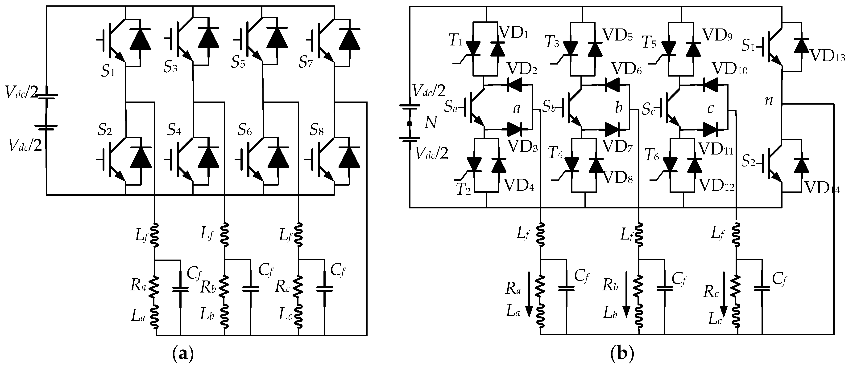
Figure 2.
Six divided segments based on the thyristor states.
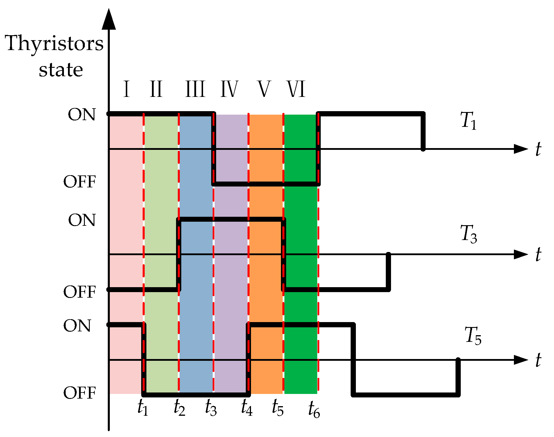
Figure 3.
Current flow path in six segments: (a) Segment I; (b) Segment II; (c) Segment III; (d) Segment IV; (e) Segment V; (f) Segment VI.
Figure 3.
Current flow path in six segments: (a) Segment I; (b) Segment II; (c) Segment III; (d) Segment IV; (e) Segment V; (f) Segment VI.

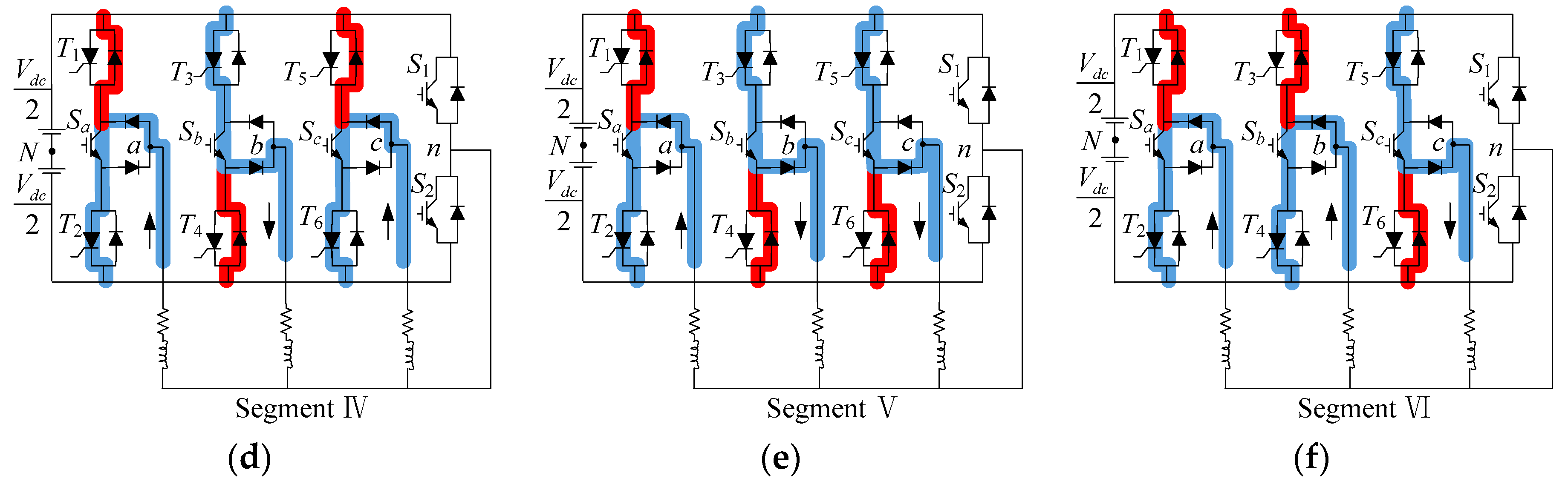
Figure 4.
Switching projection of inverter vectors in αβ plane.
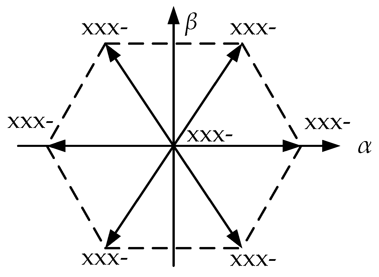
Figure 5.
Switching projection of inverter vectors in αβγ plane: (a) Segment I; (b) Segment II; (c) Segment III; (d) Segment IV; (e) Segment V; (f) Segment VI.
Figure 5.
Switching projection of inverter vectors in αβγ plane: (a) Segment I; (b) Segment II; (c) Segment III; (d) Segment IV; (e) Segment V; (f) Segment VI.

Figure 6.
Current control diagram of the proposed inverter.
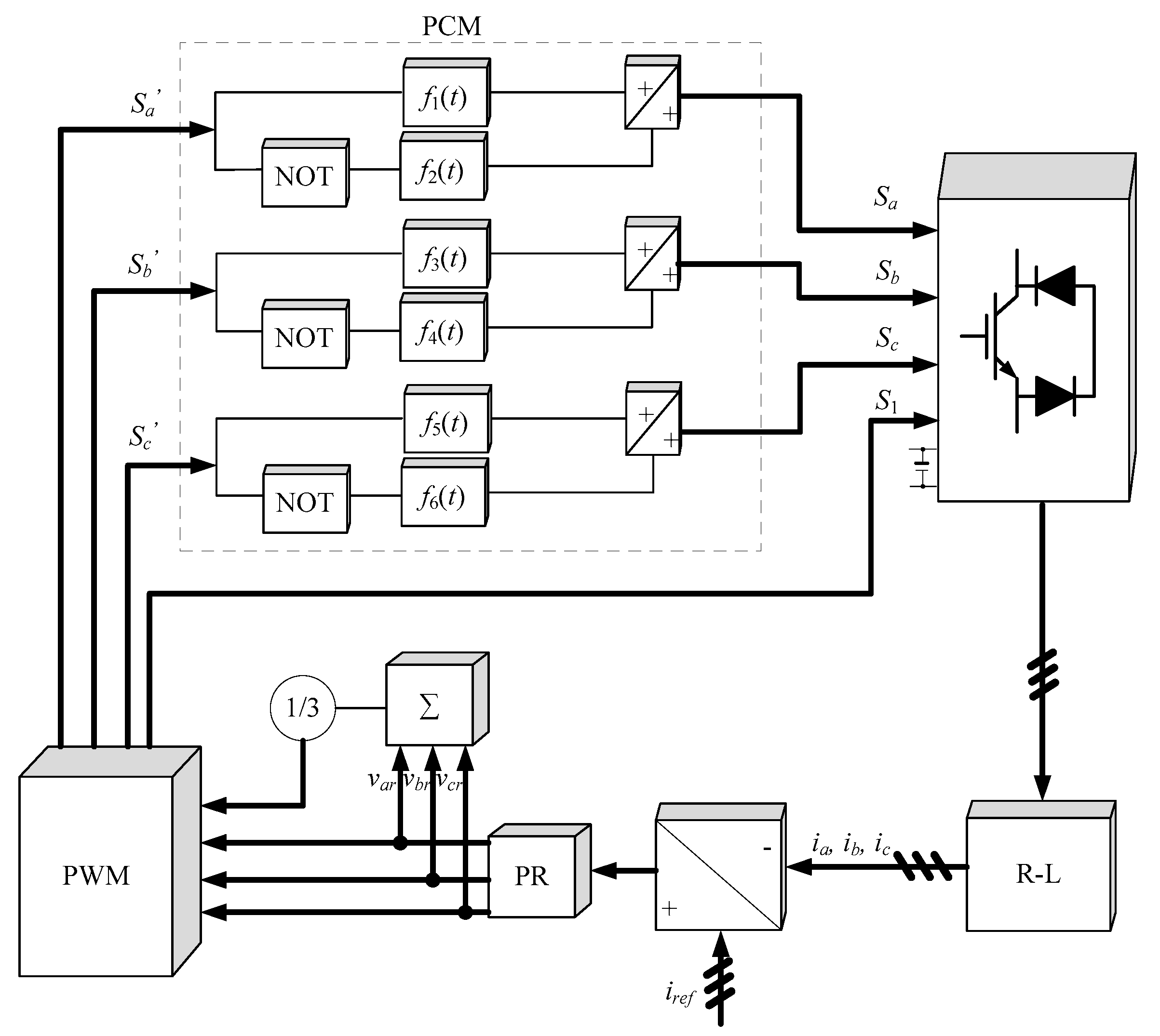
Figure 7.
Simulated results of the closed-loop current control scheme in a balanced load condition: (a) Output currents; (b) Output phase voltages; (c) Output line to line voltages; (d) THD of phase a current.
Figure 7.
Simulated results of the closed-loop current control scheme in a balanced load condition: (a) Output currents; (b) Output phase voltages; (c) Output line to line voltages; (d) THD of phase a current.
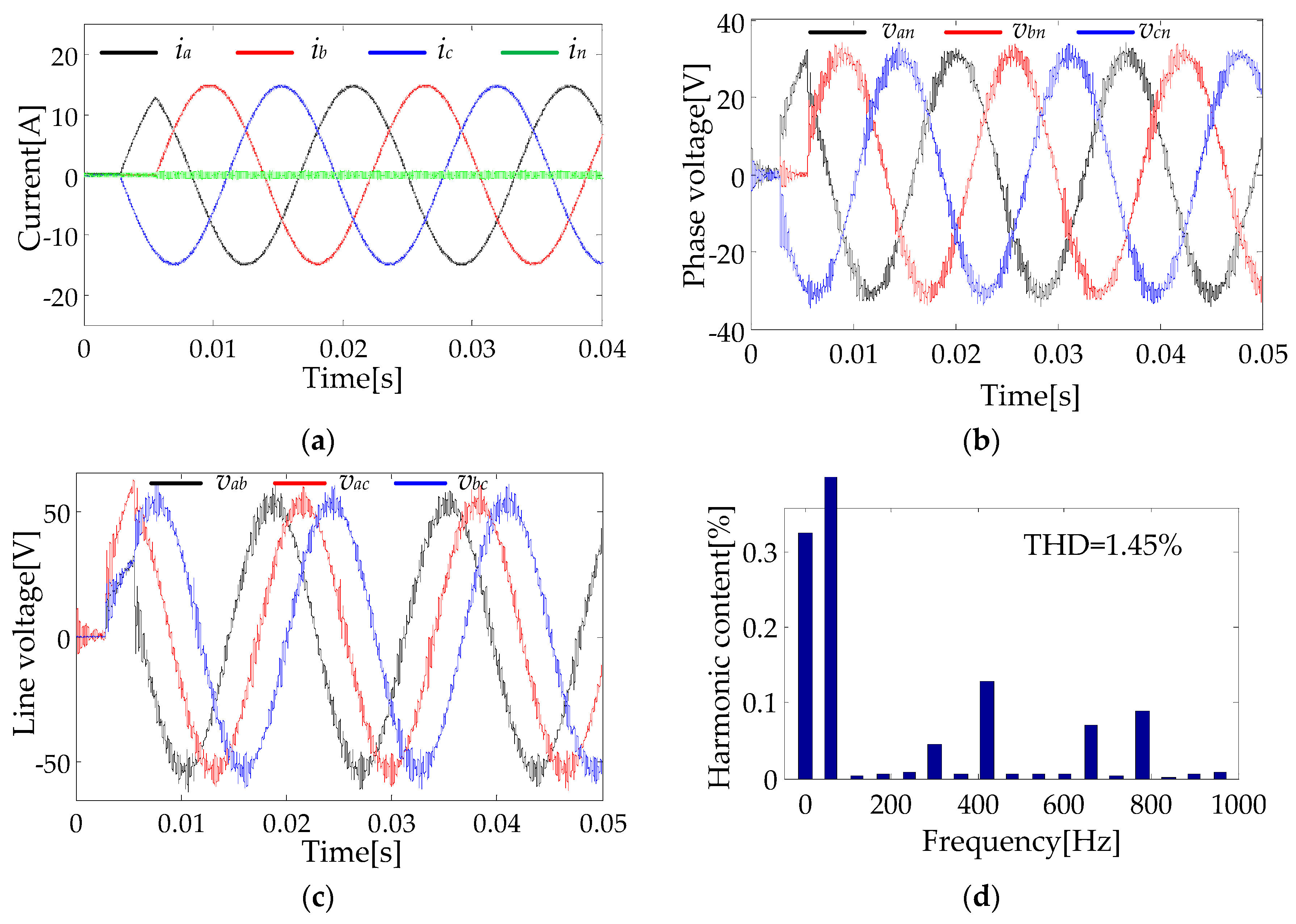
Figure 8.
Simulated results of the closed-loop current control scheme in an unbalanced load condition: (a) Output currents; (b) Output phase voltages; (c) Output line to line voltages; (d) THD of phase a current.
Figure 8.
Simulated results of the closed-loop current control scheme in an unbalanced load condition: (a) Output currents; (b) Output phase voltages; (c) Output line to line voltages; (d) THD of phase a current.


Figure 9.
Experimental prototype.
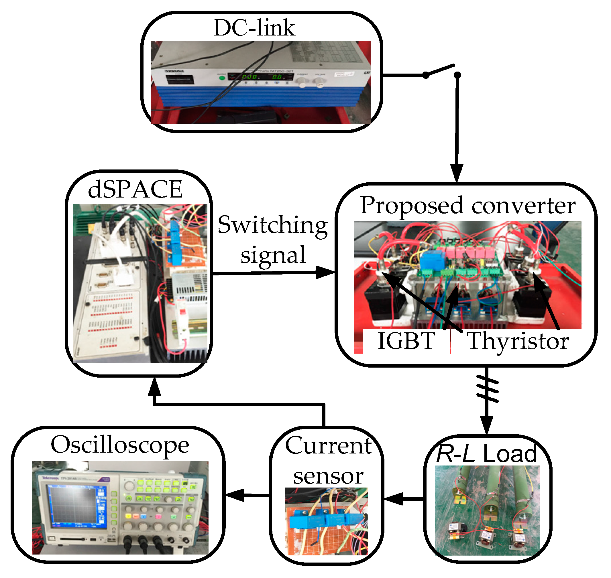
Figure 10.
Experiment results of the proposed converter: (a) Triggering pulses for phase a thyristors; (b) Output three-phase currents; (c) THD analysis of phase a current.
Figure 10.
Experiment results of the proposed converter: (a) Triggering pulses for phase a thyristors; (b) Output three-phase currents; (c) THD analysis of phase a current.


Table 1.
Switching States and Phase Voltage of Phase a.
| Switching States | Phase a | |||||||
|---|---|---|---|---|---|---|---|---|
| S1 | 1 | 0 | ||||||
| UT | 1 | 0 | 1 | 0 | ||||
| Sa | 1 | 0 | 1 | 0 | 1 | 0 | 1 | 0 |
| van | 0 | −Vdc | −Vdc | 0 | Vdc | 0 | 0 | Vdc |
Table 2.
Switching Combinations and Voltage Vectors.
| Vectors | States | van, vbn, vcn | |||||
|---|---|---|---|---|---|---|---|
| I | II | III | IV | V | VI | ||
| V0 | 0000 | 0, 1, 0 | 0, 1, 1 | 0, 0, 1 | 1, 0, 1 | 1, 0, 0 | 1, 1, 0 |
| V1 | 0001 | −1, 0, −1 | −1, 0, 0 | −1, −1, 0 | 0, −1, 0 | 0, −1, −1 | 0, 0, −1 |
| V2 | 0010 | 0, 1, 1 | 0, 1, 0 | 0, 0, 0 | 1, 0, 0 | 1, 0, 1 | 1, 1, 1 |
| V3 | 0011 | −1, 0, 0 | −1, 0, −1 | −1, −1, −1 | 0, −1, −1 | 0, −1, 0 | 0, 0, 0 |
| V4 | 0100 | 0, 0, 0 | 0, 0, 1 | 0, 1, 1 | 1, 1, 1 | 1, 1, 0 | 1, 0, 0 |
| V5 | 0101 | −1, −1, −1 | −1, −1, 0 | −1, 0, 0 | 0, 0, 0 | 0, 0, −1 | 0, −1, −1 |
| V6 | 0110 | 0, 0, 1 | 0, 0, 0 | 0, 1, 0 | 1, 1, 0 | 1, 1, 1 | 1, 0, 1 |
| V7 | 0111 | −1, −1, 0 | −1, −1, −1 | −1, 0, −1 | 0, 0, −1 | 0, 0, 0 | 0, −1, 0 |
| V8 | 1000 | 1, 1, 0 | 1, 1, 1 | 1, 0, 1 | 0, 0, 1 | 0, 0, 0 | 0, 1, 0 |
| V9 | 1001 | 0, 0, −1 | 0, 0, 0 | 0, −1, 0 | −1, −1, 0 | −1, −1, −1 | −1, 0, −1 |
| V10 | 1010 | 1, 1, 1 | 1, 1, 0 | 1, 0, 0 | 0, 0, 0 | 0, 0, 1 | 0, 1, 1 |
| V11 | 1011 | 0, 0, 0 | 0, 0, −1 | 0, −1, −1 | −1, −1, −1 | −1, −1, 0 | −1, 0, 0 |
| V12 | 1100 | 1, 0, 0 | 1, 0, 1 | 1, 1, 1 | 0, 1, 1 | 0, 1, 0 | 0, 0, 0 |
| V13 | 1101 | 0, −1, −1 | 0, −1, 0 | 0, 0, 0 | −1, 0, 0 | −1, 0, −1 | −1, −1, −1 |
| V14 | 1110 | 1, 0, 1 | 1, 0, 0 | 1, 1, 0 | 0, 1, 0 | 0, 1, 1 | 0, 0, 1 |
| V15 | 1111 | 0, −1, 0 | 0, −1, −1 | 0, 0, −1 | −1, 0, −1 | −1, 0, 0 | −1, −1, 0 |
Note: The unit of the output voltage is Vdc.
Table 3.
Key Parameters of Simulation System.
| Parameters | Values |
|---|---|
| DC link voltage | 100 V |
| AC filter inductor for each phase | 5 mH |
| Ac filter capacitor for each phase | 1.5 µF |
| Switching frequency | 5 kHz |
| Load inductor | 1.5 mH |
| Load resistor | 3-phase variable resistors |
Table 4.
Specifications of Switches.
| Item | IGBT Module (Single Switch) | IGBT Module (Dual Switch) | Thyristor | Diode |
|---|---|---|---|---|
| Model | FZ1800R16KF4 | FF1800R17IP5 | Y60KPE | ZP2000A |
| Cost (USD) | 550 | 965 | 50 | 30 |
| Size (H × W × D, cm) | 3.81 × 19.0 × 14.0 | 3.8 × 23.4 × 8.9 | 6.0 × 15 × 5.0 | 3.2 × 9.9 × 9.9 |
| Weight (kg) | 2.31 | 1.4 | 0.85 | 0.52 |
| Ir (Amps) | 1800 | 1800 | 1800 | 2000 |
| Vr (Volts) | 1600 | 1700 | 1800 | 5000 |
Table 5.
Comparison between Proposed and Conventional Inverter.
| Item | Proposed Inverter | Conventional Inverter |
|---|---|---|
| Overall size (cm3) | 8268.4 | 3165.56 |
| Overall weight (kg) | 15.05 | 5.6 |
| Cost (USD) | 2766 | 3860 |
© 2017 by the authors. Licensee MDPI, Basel, Switzerland. This article is an open access article distributed under the terms and conditions of the Creative Commons Attribution (CC BY) license (http://creativecommons.org/licenses/by/4.0/).
Share and Cite
MDPI and ACS Style
Luo, Y.; Liu, C.; Yu, F.; Lee, C.H.T. Design and Evaluation of an Efficient Three-Phase Four-Leg Voltage Source Inverter with Reduced IGBTs. Energies 2017, 10, 530. https://doi.org/10.3390/en10040530
AMA Style
Luo Y, Liu C, Yu F, Lee CHT. Design and Evaluation of an Efficient Three-Phase Four-Leg Voltage Source Inverter with Reduced IGBTs. Energies. 2017; 10(4):530. https://doi.org/10.3390/en10040530
Chicago/Turabian StyleLuo, Yixiao, Chunhua Liu, Feng Yu, and Christopher H.T. Lee. 2017. "Design and Evaluation of an Efficient Three-Phase Four-Leg Voltage Source Inverter with Reduced IGBTs" Energies 10, no. 4: 530. https://doi.org/10.3390/en10040530
Note that from the first issue of 2016, this journal uses article numbers instead of page numbers. See further details here.