
A Short-Current Control Method for Constant Frequency Current-Fed Wireless Power Transfer Systems

School of Automation, Chongqing University, 174 Shazheng Street, Shapingba District, Chongqing 400030, China
*
Author to whom correspondence should be addressed.
Energies 2017, 10(5), 585; https://doi.org/10.3390/en10050585
Submission received: 24 February 2017
/
Revised: 15 April 2017
/
Accepted: 20 April 2017
/
Published: 25 April 2017
(This article belongs to the Special Issue Wireless Power Transfer and Energy Harvesting Technologies)
Abstract
:Frequency drift is a serious problem in Current-Fed Wireless Power Transfer (WPT) systems. When the operating frequency is drifting from the inherent Zero Voltage Switching (ZVS) frequency of resonant network, large short currents will appear and damage the switches. In this paper, an inductance-dampening method is proposed to inhibit short currents and achieve constant-frequency operation. By adding a small auxiliary series inductance in the primary resonant network, short currents are greatly attenuated to a safe level. The operation principle and steady-state analysis of the system are provided. An overlapping time self-regulating circuit is designed to guarantee ZVS running. The range of auxiliary inductances is discussed and its critical value is calculated exactly. The design methodology is described and a design example is presented. Finally, a prototype is built and the experimental results verify the proposed method.
1. Introduction
Wireless Power Transfer (WPT) technology utilizes high frequency magnetic fields to realize energy transfer. This can eliminate the risk of sparks and electrical shocks and make the power transfer process safe and convenient. In recent years, this technology has seen more and more applications in EV charging, biomedical implants and consumer electronics [1,2,3,4,5,6].
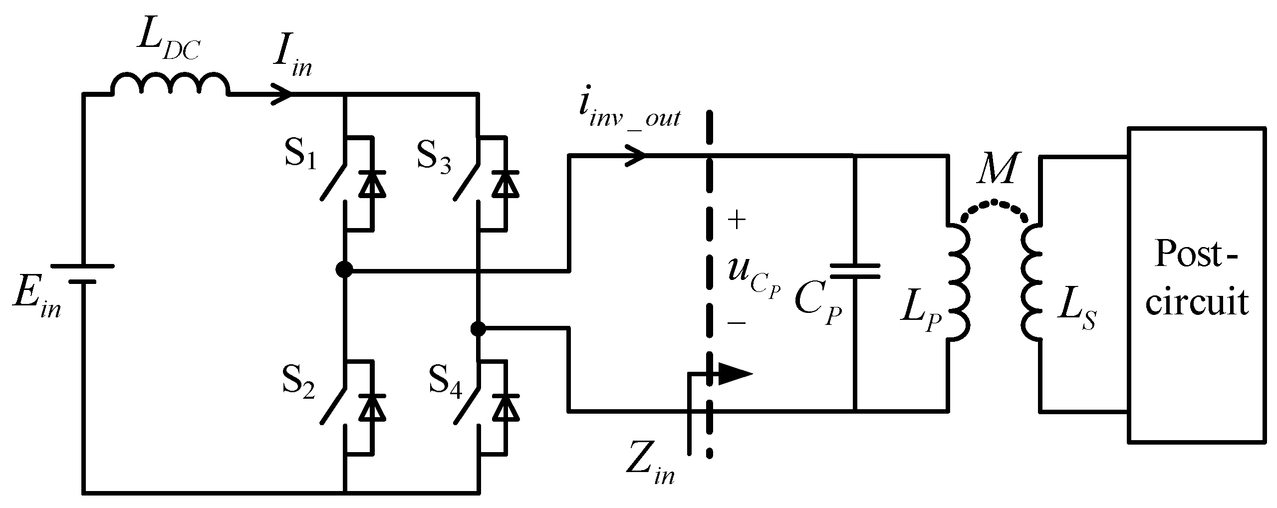
Figure 1 illustrates a typical Current-Fed WPT system. A DC voltage source and inductance compose a quasi-current source. A parallel resonant network is used on the primary side. The post-circuit contains a resonant network, rectifier, filter and load. Series, parallel or other types of resonant network can be used on the secondary side of a WPT system.
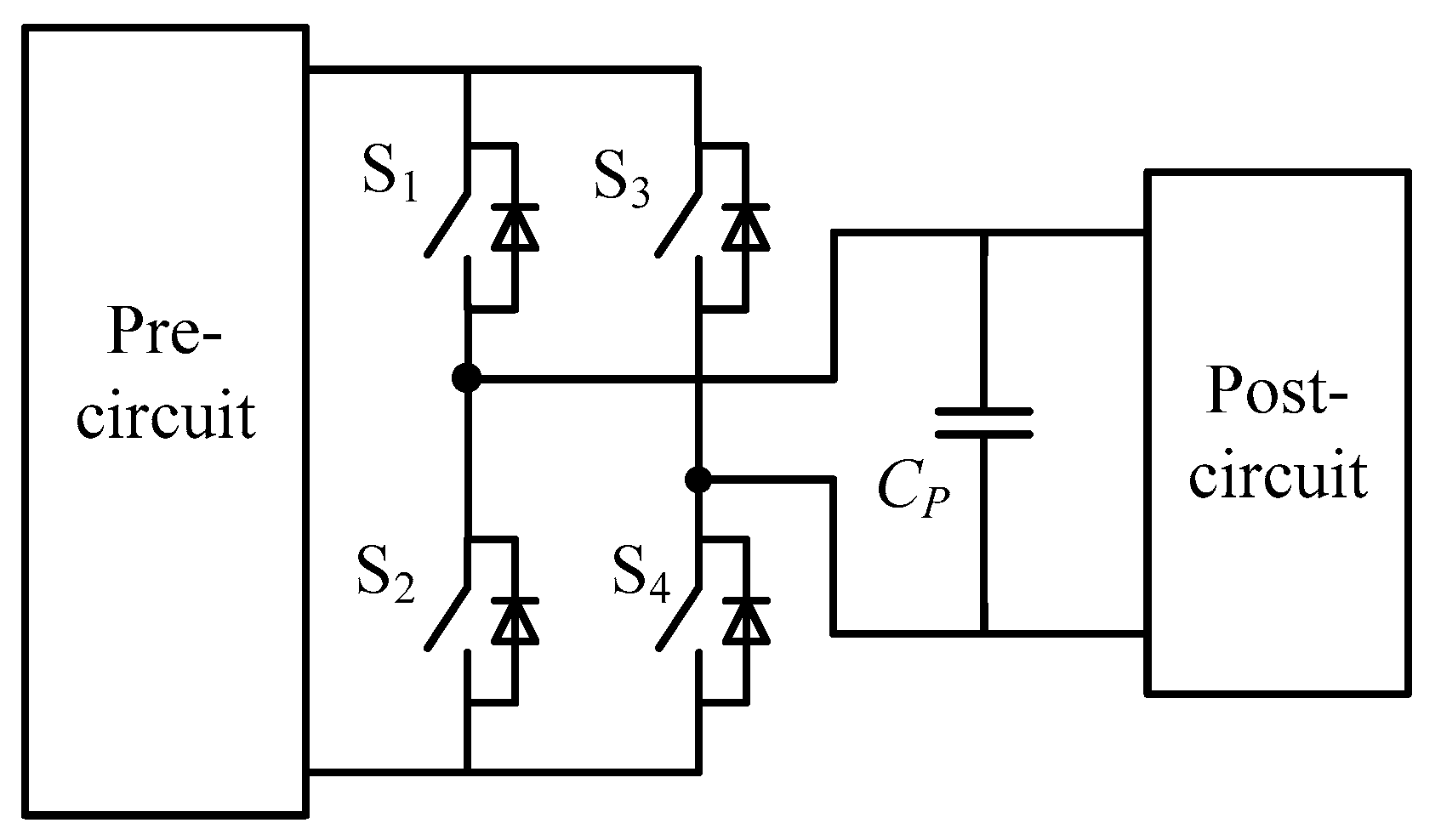
In the above system, the parallel-resonant capacitor has the risk of being shorted by switches. If this happens, a large short current will be generated in the inner loop between the inverter and resonant tank. Mismatch between the Zero Voltage Switching (ZVS) frequency () and operation frequency () will lead to a short current. The existence of short currents will damage the switching components and greatly increase the risk of breakdown of the whole system. Generally, a short current is a common phenomenon in the topology shown in Figure 2.
One typical type of application circuit is a high step-up converter [7,8]. In these converters, represents the parasitic capacitance of a high turn-ratio transformer. Another typical application circuit is the parallel resonant converter. The Current-Fed WPT system is a parallel resonant converter.
For a Current-Fed WPT system, frequency drift is an important issue [9,10]. Mutual inductance and load resistance change dynamically, which means cannot be a constant value. Calculation of the ZVS frequency is a complicated and time-consuming process [11,12]. Moreover, real-time load and mutual inductance identification methods also require complex calculations and detection circuits [13,14], so some real-time and simple methods need to be used.
By using a passive zero crossing point detection method such as the ZVS method, operation frequency can keep up with in real-time [9,10,15]. However, due to the time lag on the detection route, there exists a mismatch between and . Other methods including active frequency tracking [16] and the self-oscillating switching technique [17] are also proposed to reduce short currents. A common property of these methods is that the operating frequency is time-variant in order to track . This makes filter design difficult. Another disadvantage of these methods is the frequency-bifurcation phenomenon [12], which will cause a significant decrease of transferred power.
To eliminate short currents and achieve constant frequency operation simultaneously, the classical method utilizes four blocking diodes placed in series with switches to cut off the loops of short current flows [9], which increases the energy losses and costs.
This paper proposes an inductance damping method for Current-Fed WPT systems. The inductance is connected in series with the parallel resonant network. Short currents are suppressed, while no extra switching component needs to be added. All switches of the inverter are ZVS. Most importantly, the method hardly affects the input and output characteristics of the original Current-Fed WPT system. Operation conditions of the system are discussed, including operation frequency, overlapping time and value of L1. Based on the conditions, a design methodology is proposed to apply the method to traditional Current-Fed WPT systems.
The rest of this paper is organized as follows: Section 2 briefly introduces the mechanism of short current formation in Current-Fed WPT systems. The proposed inductance damping method is elaborated in Section 3. The circuit and its cyclical switching operation are presented. In Section 4, operating conditions governing the use of the proposed method are listed and explained. An overlapping-time self-regulating circuit is described to satisfy the second operation condition in Section 5. Section 6 discusses the range of , and the critical value is calculated exactly. The design procedure and an example are given in Section 7. The experimental results obtained on a 60 W prototype are presented.
2. Mechanism of Short Current
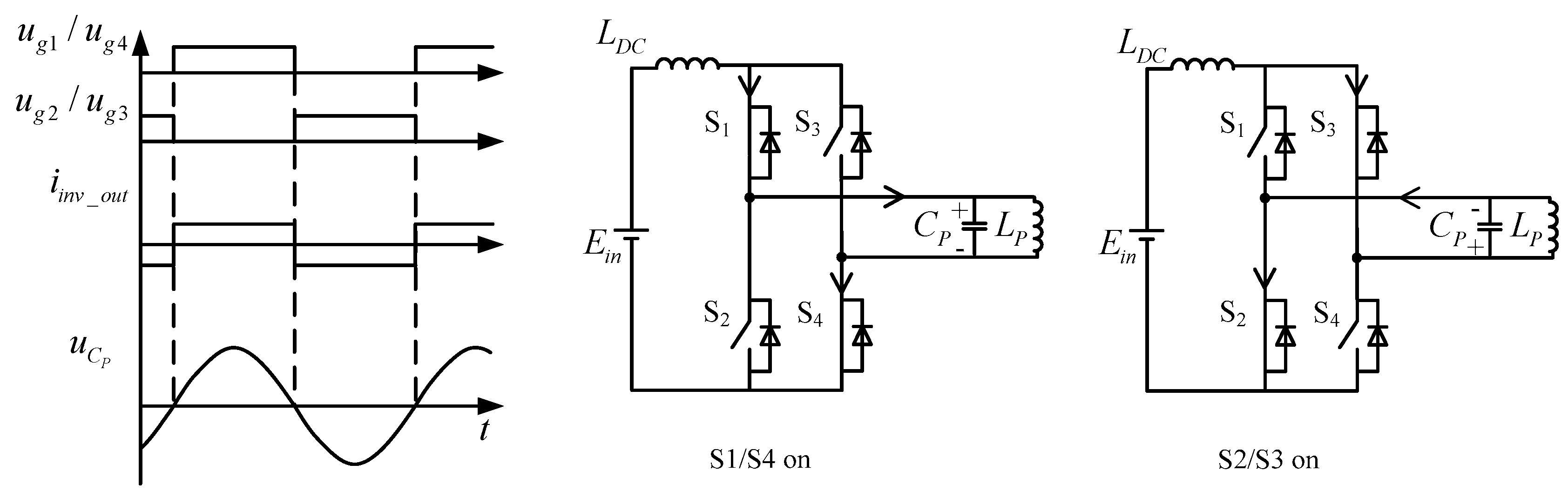
As shown in Figure 1, the voltage source and large DC inductor comprise a quasi-current source. Two switching pairs (S1/S4 and S2/S3) operate complementarily to inject a square wave current into the parallel resonant tank (composed of and ). When the operating frequency equals , the switching instants are accurate on the zero crossing point of the resonant voltage . The corresponding waveform and circuit are illustrated in Figure 3.
For the resonant network, ZVS frequency is close to the zero phase angle resonant frequency [9,11]. Because is easier to calculate than , can be replaced by in the following analysis. is calculated by:
As illustrated in Figure 1, is the input impedance of the resonant network under the operation frequency . Therefore, when equals , the resonant network is purely resistant and the short current is eliminated. If drifts away from , a frequency drift will happen, and a short current will be generated. According to the different loops of short current, short currents can be divided into two types:
A. Capacitive case,
In this case, the resonant network is resistive-capacitive () when drifts away from . The AC input voltage is lagging the fundamental harmonic of the AC input current . When reverses its direction, has not reached its zero point. The change of switches’ state generates a path to short . As a result, the generated short current is extremely high. The instantaneous short current may damage the switch devices. This is shown in Figure 4a.
Generally, the resonant network is resistant-capacitive when is higher than , since a parallel network is used on the primary side. This case is called “higher case”.
B. Inductive case,
Meanwhile, in the inductive case, the resonant network is resistive-capacitive () when deviates from . The AC input voltage is led to the fundamental harmonic of the AC input current . When reaches its zero point, has not reversed its direction. A loop is generated to clamp to 0 V. The short current will be clamped to track the current (flowing in ). The waveform and short circuit in this case are shown in Figure 4b.
Generally, the resonant network is resistant-inductive when is lower than . This case is called “lower case” in [16]. From the above analysis, a criterion is proposed to eliminate short currents in circuits that have the same topology as Figure 2:
- When , S2 and S3 must remain in an off state.
- When , S1 and S4 must remain in an off state.
If the criterion is broken, a short current will appear. Comparing the two cases, the capacitive case is more dangerous to the switching devices because short current in this case is uncontrollable. The inductive case is relatively safe because the short current can be clamped to a certain value (the current flowing in ).
3. The Proposed Inductance-Damping Method
Figure 5 shows a typical current-fed WPT system topology with the proposed inductance-damping method. Inductor is connected in series with the resonant network. is placed in the loop of the short current and will dampen any high di/dt ratio generated by a short current.
On the primary side, the topology of the proposed circuit is similar to a LCL network, but it works in an absolutely different way. In an LCL network, is a resonant component. However, in the proposed circuit, is not a resonant component. It is used to smooth the short current during the commutation period During the other switching cycle periods, it undertakes the DC current .
Figure 6 shows the theoretical waveform of the circuit over a steady-state cycle. S1 and S4 are switched with the same pulse, while S3 and S4 are switched with the other pulse. Turn-on signals of S1/S4 and S2/S3 have a phase difference of 180°.
Compared with the PWM pulse in Section 2, the turn-off signals of S1/S4 and S2/S3 are delayed by . That is, an overlap time is added to the PWM sequence, which means each switch is in the on state during the period. In addition, to guarantee the generation of a short current in the capacitive case, the frequency of the PWM frequency must satisfy:
Generally, need to be higher than to satisfy (2). Since operation and the waveform under steady state conditions are symmetrical in every half cycle, the equivalent circuit of every operation mode between and is illustrated in Figure 7.
Normally due to the frequency selection ability of the resonant network, the voltage of can be considered as its fundamental component. When is selected as the origin of a cycle, can be represented as:
where .
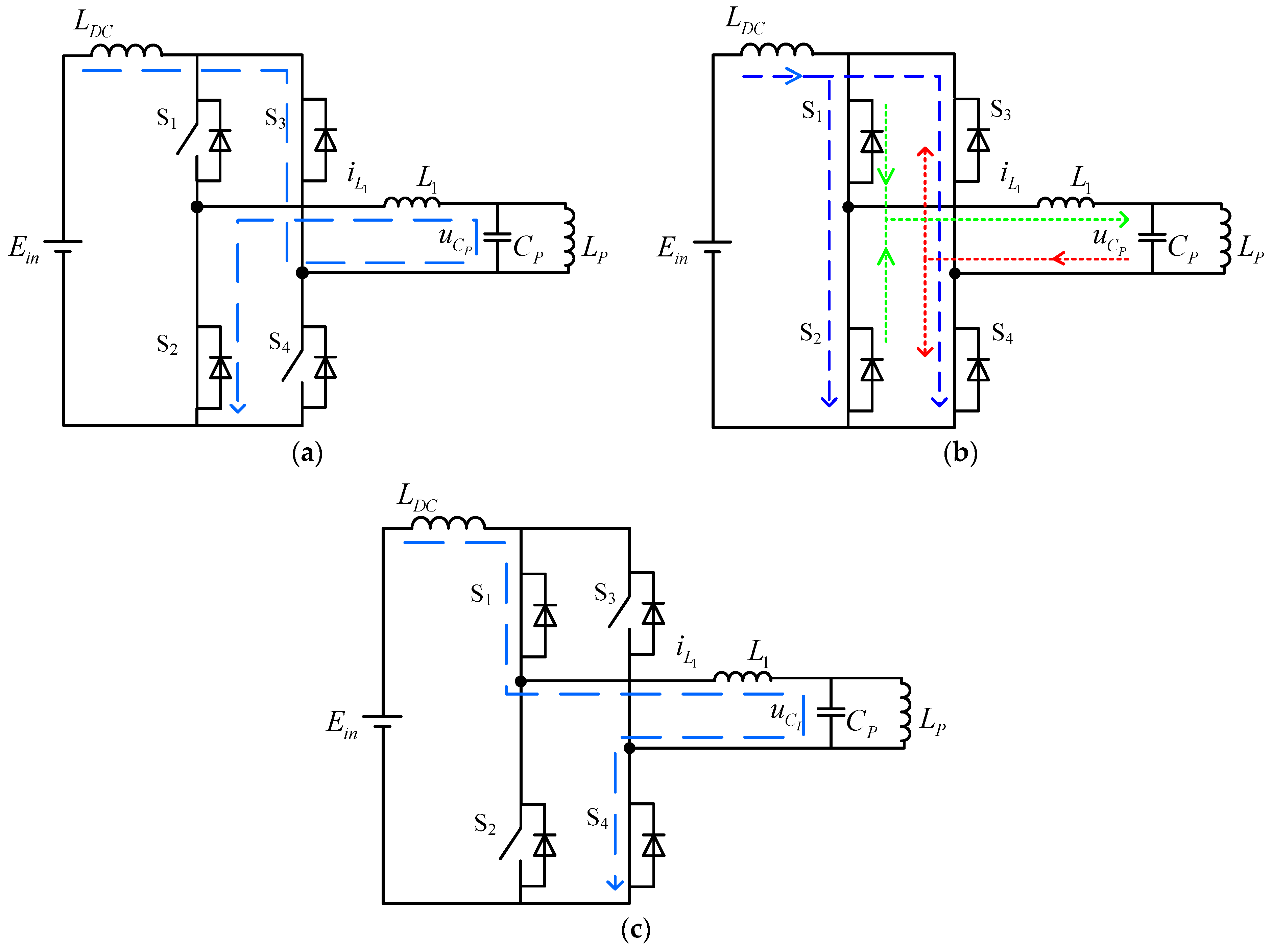
A. Mode 0: Before , Figure 7a
In the mode, S2 and S3 are in the on state, S1 and S4 are in the off state. The voltage of S1 and S4 is equal to the absolute value of . The current flowing through () is equal to .
B. Mode 1: , Figure 7b, Overlapping Period/Commutation Period
In this mode, changes its direction smoothly, and no voltage spike is generated. At , S1 and S4 turn on, and the four switches are all on. This means the resonant network and power supply are in the short mode. is connected in parallel with . So:
Because is negative, the current of starts to increase from to positive:
In the mode, the current flowing in each switch is the combination of the input current and short current . We have:
As can be seen in Figure 6, current flows through S1 and S4, increases from 0 to positive gradually after . Therefore, S1 and S4 turn on with ZCS.
At , crosses the zero point.
At , increases to , and decreases to 0. After , is higher than . It means is reversed to negative.
At , is equal to 0, reaches its peak and starts to decrease:
At , decreases to , and S2/S3’s anti-parallel diodes turn off.
When S2 and S3 turn off between and , the reversed current will flow through their anti-parallel diodes. As a result, S2 and S3 can turn off with ZVS, so the switches’ overlap time should satisfy:
C. Mode 2: , Figure 7c, Energy-input Period
In this mode, is equal to the input current and stays constant. Considering the inductor is usually designed small, is nearly equal to . Thus energy from is input to the resonant network. Operation in the remaining half switching cycle is symmetrical to the previous four operation modes. Therefore, the four switches S1–S4 can all turn on with ZCS and turn off with ZVS.
4. Steady-State Analysis and Operation Conditions
4.1. Steady-State Analysis
Because of the high order and resonant characteristics, the accurate steady state model becomes extremely complex and is not suitable for design. The paper proposes an approximate modeling method by ignoring the short overlap time in a cycle. The detailed analysis is as follows:
Since can be considered as a standard sinusoid, the system can be divided into two parts, the switching network and the resonant network. As illustrated in Figure 8, for the switching part, the post-circuit can be regarded as an AC load ; for the resonant part, the pre-circuit can be regarded as an AC source .
As shown in Figure 6, during the first half cycle, can be written as:
Output power of power supply can be derived:
Output power of inverter is:
Considering that most of the power is transferred by the fundamental harmonics, the input power of resonant network can be derived:
Phase difference between and fundamental harmonic of is the same as the impedance angle of resonant network ():
In (13), is the impedance of circuit in secondary side, which is relative to the resonant network and load. Compared with the switching period , the short overlap time between and can be ignored. Thus, , (11) and (12) can be simplified:
Ignoring the loss of , inverter and , we have:
Using (10), (12), (14) and (15), we have:
Equations (17) and (18) can be used to consider the voltage and current stress of switches and passive components. Equation (19) can be used to approximately calculate the power that is transferred to the load.
4.2. DC Voltage Gain
In the system, input-output voltage gain () can be divided into two parts: voltage gain of the inverter and voltage gain of the rest circuit. Voltage gain of the inverter is derived by:
When and are small enough, (19) is simplified:
Voltage gain of the rest circuit is related to the circuit in secondary side. In Section 7, input-output voltage gain of the experimental system is derived.
4.3. Operation Condition
In order to achieve the expected operation in the proposed circuit, three conditions need to be guaranteed.
4.3.1. Operation Frequency
Since the proposed method in the paper is applied to reduce the short current in the capacitive case, must be resistive-capacitive. Thus, needs to satisfy (2) under all load and all mutual inductance conditions, from rated load to light load and from rated coupling to lighter coupling. Generally, when is higher than , Equation (2) is satisfied.
If is resistive-inductive (generally when ), the peak value of short current will be suppressed in this situation because of the damping of . However, switches will sustain high voltage spikes during the switching time to change the direction of , so this is not a normal operation mode.
4.3.2. Duty Ratio of PWM Pulses
S2 and S3 must turn off between and to guarantee ZVS running. That is, the two switches needs to turn off during the period when is higher than . The duty ratio of PWM pulses need to satisfy:
It is complex to calculate the exact value of and because the system is under resonant state. Moreover, when load and mutual inductance vary, and are changed. It means the final D needs to satisfy (21) under all load and mutual inductance condition. A simple strategy is used to satisfy the condition in all load and inductance conditions, which is carefully described in Section 5.
4.3.3. Value of
Peak value of must be higher than input current to guarantee that the two switches turn off with ZVS. If is too large, the peak value of during the commutation period is lower than . In the case, has to hop from a value to in the turn-off transition of the two switches. Large voltage spikes are imposed on the switches. Figure 9 shows system’s waveforms in this situation. Fortunately, because of the existence of the Collector-to-Emitter capacitor in switches and junction capacitors in their anti-parallel diodes, the peak value of the voltage will be suppressed. This is because the parasite capacitor can absorb the high voltage spike and make the voltage transient smoother. The critical value of is calculated in Section 6.
If the above conditions are satisfied, the short current can be dumped and switch voltage spike he will be eliminated.
5. Overlapping Time Self-Regulating Circuit
The turn-off time of the two on-state switches must happen between and to satisfy the second condition listed in Section 4. An automatic overlapping-time regulator is proposed to guarantee the turn-off time happens between and . Because and is short (usually below 1 μs), the regulating circuit should be extremely fast.
In this paper, a simple but effective implement is fabricated based on the principle pointed in Section 3. When reach its peak at , will definitely cross its zero point, and must be between and . If the switch can turn off at the moment when crosses the zero point, soft commutation can be achieved. In implementation, only a high-speed zero-crossing comparator is needed to detect the moment when crosses the zero point. The implementation diagram that automatically regulates the overlapping-time is shown in Figure 10.
Considering time delay in the zero-crossing comparator and driver, a phase-lead compensator is used to compensate the time delay. Two phase-lead networks are generally used in practice [18], which is also shown in Figure 10. Network 1 is used in the experimental circuit to compensate the time delay.
6. Range of L1 and the Critical Value
In the proposed system, is an important circuit component. The value of must be considered carefully. During the commutation period, if is too large, the peak value of is lower than and soft commutation fails. If is too small, the peak value of is too high to damp the short current. Therefore, the range of needs to be ascertained, and the boundary value of needs to be calculated exactly. The proper value of needs to be considered based on that.
A special operation situation (the critical mode) of the system is observed and used to confirm range of .In the critical mode, peak value of equals to . Value of in this situation is the boundary value of —called . Waveform of the critical mode is shown in Figure 11.
In the critical mode, .
during the commutation period is derived by:
At , is equal to zero and reaches its peak value:
During the first half cycle, can be written as:
In the second half cycle, is the negative value of the first half cycle. So the fundamental component of () is derived by Fourier series, we have:
is the phase angle of , which takes as a reference.
Then we have:
In the mode, (11) is simplified:
Equations (15) and (27) make up a simultaneous equation set. Thus, , and can be calculated by a numerical algorithm simultaneously.
must be lower then to satisfy the third operation condition, so we have:
A value of that is slightly lower than is suitable, since the operation conditions are satisfied while performance of the proposed method is guaranteed.
7. Design Procedure, Example and Measurements
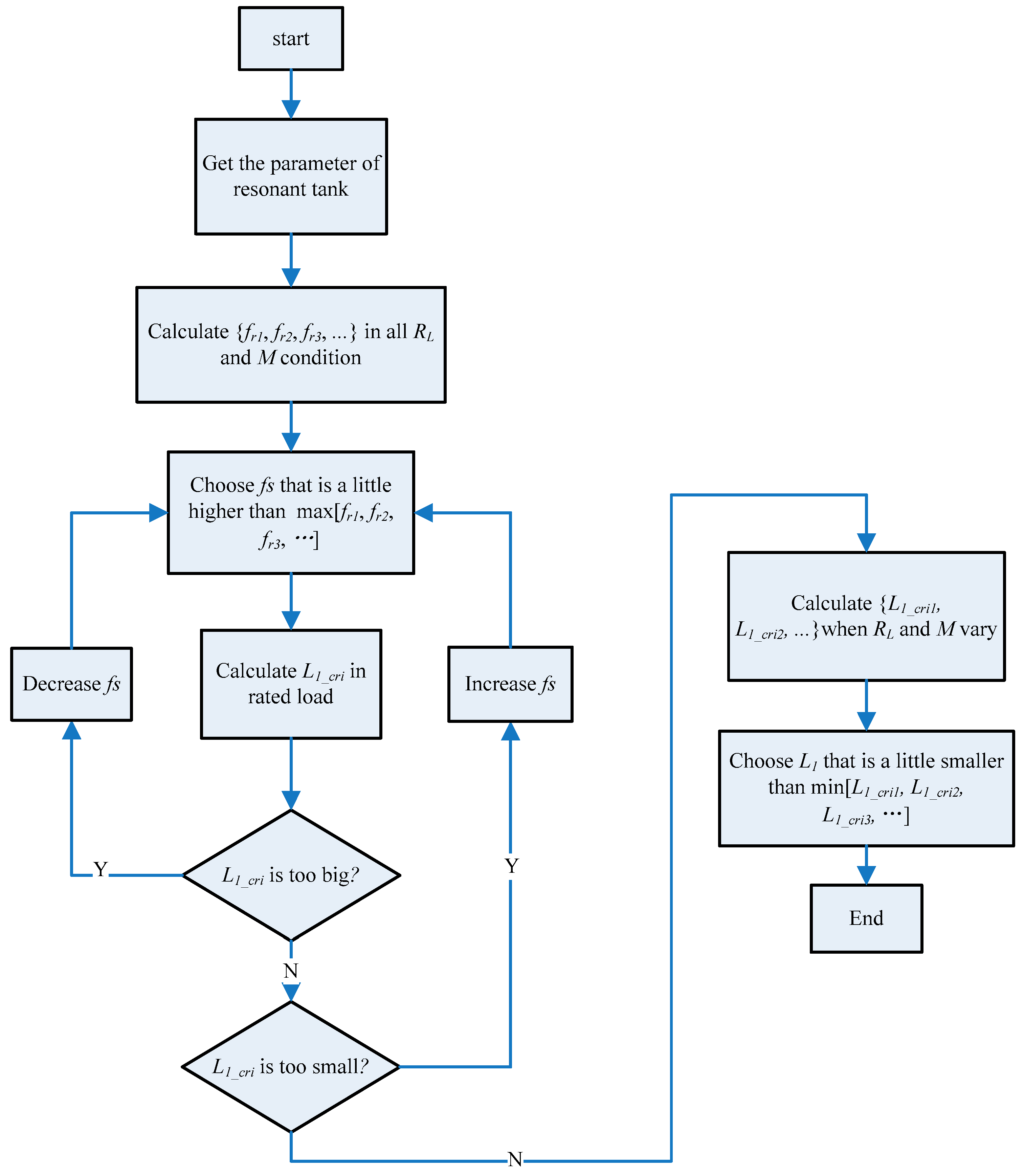
7.1. Design Flowchart
When applying the proposed method to a traditional Current-Fed IPT system, and need to be considered. The criterion of choosing and is that the system must operate normally when resonant components and loads vary. The design procedure is shown in Figure 12.
7.2. Design Example
A 60 W experimental system was built using the proposed method. Its parameters are listed in Table 1. The new system is designed using the strategy in Figure 12.
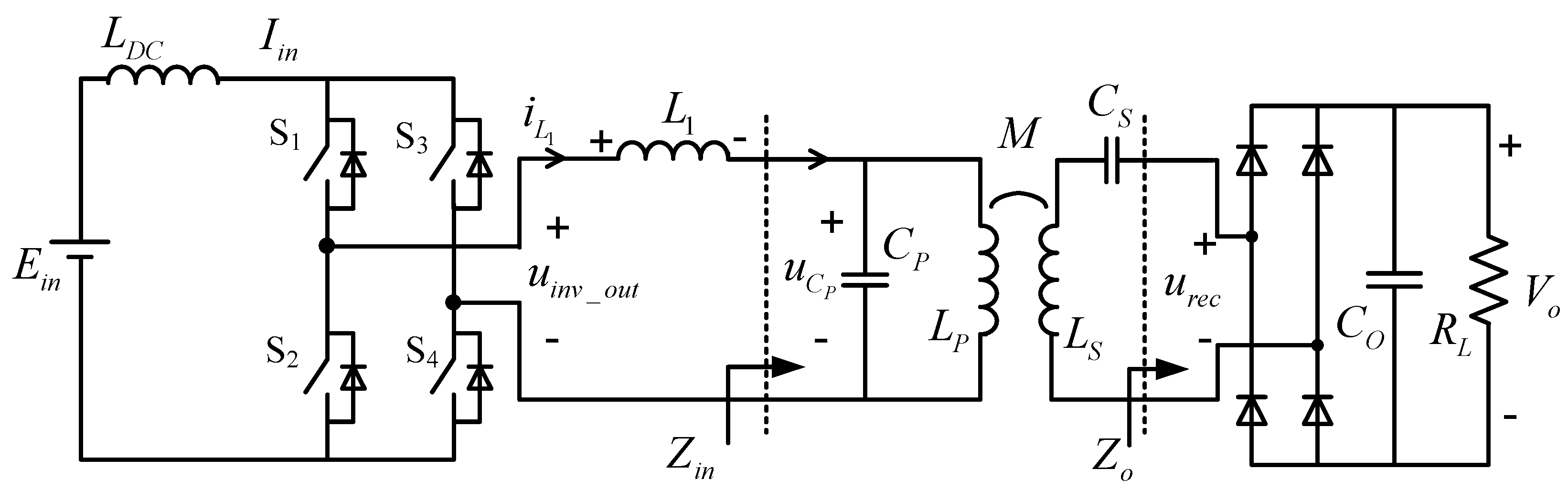
In the experimental system, the series network used on the secondary side is taken as an example, as illustrated in Figure 13. It must be mentioned that application of the proposed method is irrelevant to the type of network used on the secondary side. Moreover, the type of network on the secondary side is irrelevant to the analysis approach and design methodology.
In the circuit:
is the equivalent AC impedance of the rectifier and its post-circuit, which can also be regarded as the AC equivalent AC load of the system. Generally, the equivalent load is considered to be purely resistant, and is calculated by:
The input-output voltage gain () of the experimental system can be divided into three parts: voltage gain of the inverter, voltage gain of the resonant network and voltage gain of rectifier. Voltage gain of inverter has been given in (20). Voltage gain of the resonant network is derived by:
is peak value of the fundamental component of the rectifier’s input voltage .
When is large enough and is small enough, Equation (33) is simplified:
The voltage gain of the rectifier and filter is:
Thus, the voltage gain of the whole system is derived:
Equation (34) shows that the voltage gain of the whole system is independent of the load and when is large enough and is small enough. However, the calculation result of the above model has a big error when calculating using the equation set in Section 6. Since there exists some distortion in the secondary current , the equivalent load cannot be regarded as a pure resistance and simply calculated using Equation (30). Based on the extended fundamental frequency analysis method [19], a more accurate is derived:
Replacing (30) with (35), the exact value of can be obtained.
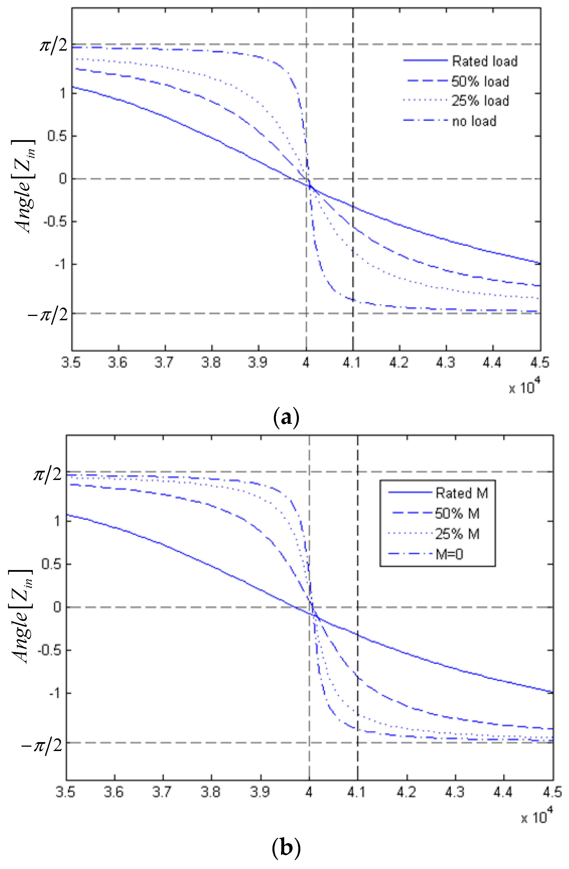
The relationship between and of the experimental system is drawn in Figure 14. The zero phase angle resonant frequencies for different loads and mutual inductance conditions are all near 40 kHz. When is chosen to be higher than 40 kHz, are all negative under different load conditions. 41 kHz is chosen to be the operation frequency since remains negative when the load changes from heavy to light ( increases continuously) and the mutual inductance changes from the rated coupling to loose coupling.
Next, the proper value of is considered. The first thing is calculating at the rated load and coupling (). In this case, .
Then calculate when and vary. The results are shown in Figure 15. When varies from rated load to light load, the correspondent increases monotonously. When the mutual inductance varies from rated coupling to weak coupling, the corresponding increases monotonously. Therefore, if is equal to or lower than 6.87 μH, the third operating condition will be naturally achieved when and vary.
Considering the error of measurement and modeling, needs to be smaller than 6.86 μH to guarantee the third operating condition. In this experimental system, the value of is 3.85 μH.
7.3. Experiment and Performance
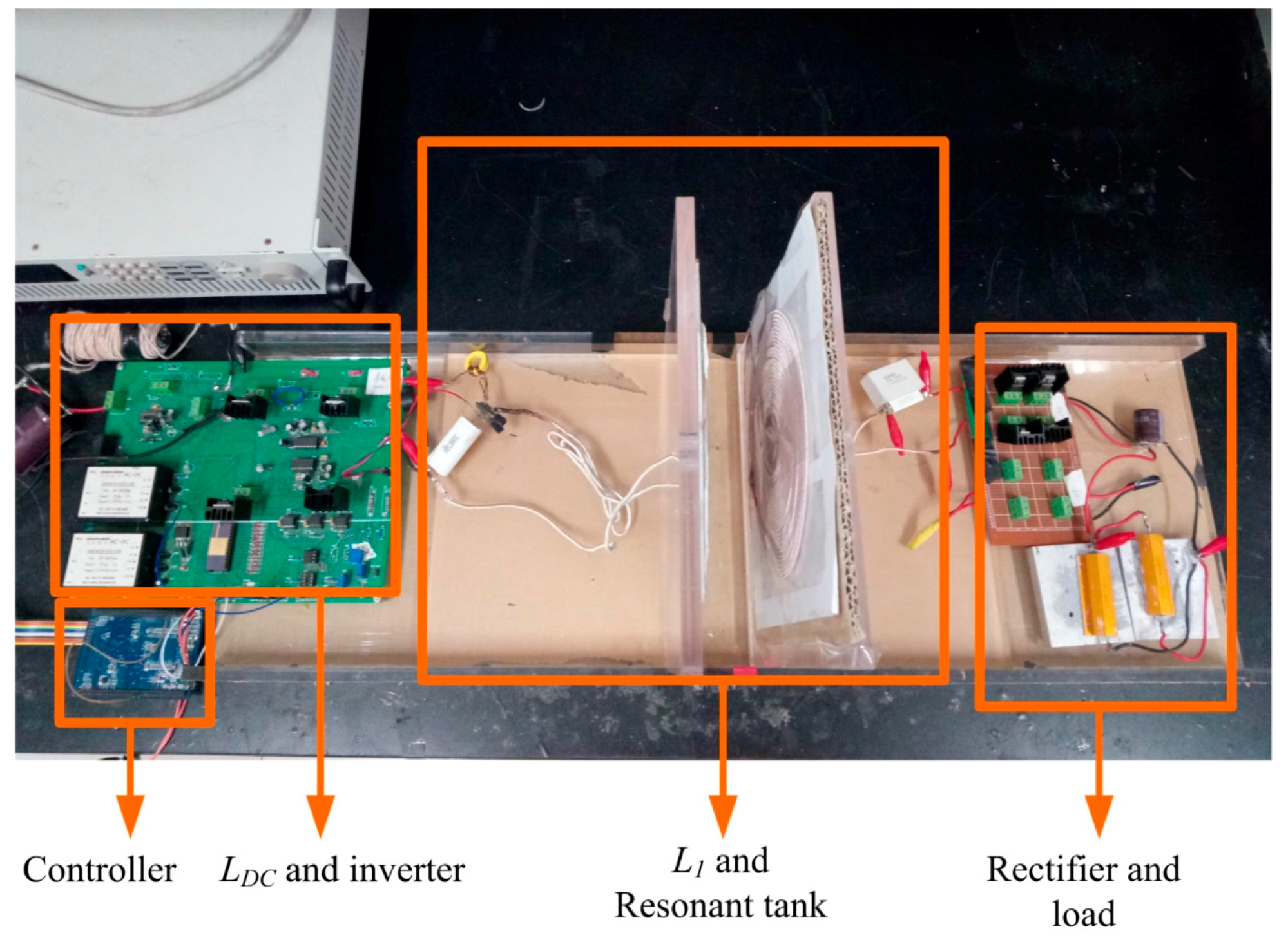
A proposed 60 W Current-Fed WPT prototype is built to verify the method. The experimental system is set up as shown in Figure 13. The switching components used are IGBT FGA25N120ANTD and STPS20120D diodes. The driving signals are produced by a TMS320X2812 DSP. Photos of the prototype system are shown in Figure 16 and Figure 17.
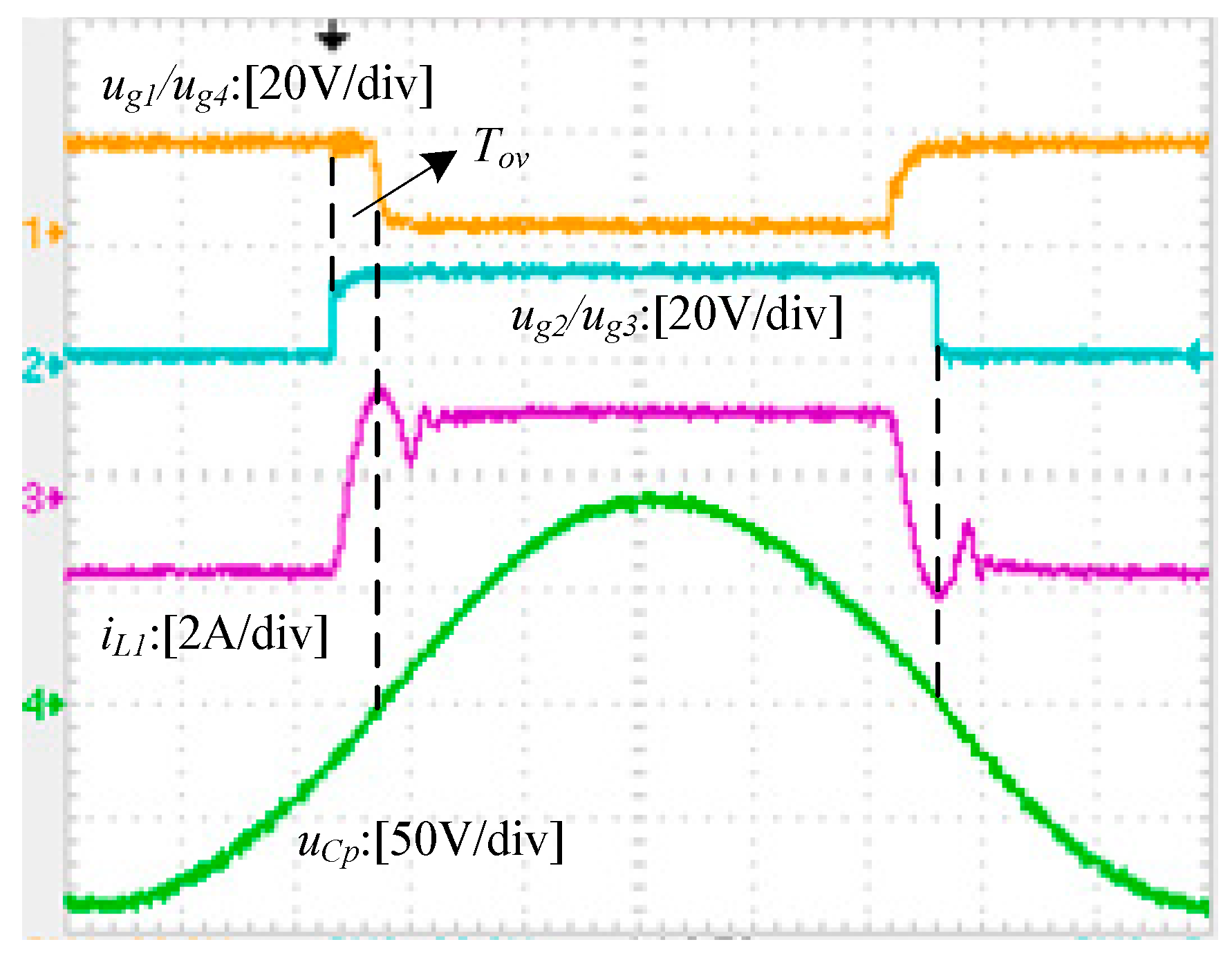
Figure 18 shows a comparison of the measured waveforms at rated load. Short currents are greatly damped in the system with the proposed method. The peak value of the short current in a traditional system is several times higher than , while the short current in the system with the proposed method is kept at a very low level.
Due to parasitic capacitance in the switches and junction capacitors in their anti-parallel diode, a current oscillation exists in after t4. Figure 18c illustrates the waveform of the system with the proposed approach when = 6.40 µH. In this situation, the peak value of the short current is nearly equal to Iin, which verifies the accuracy of the model in Section 6. As shown in Figure 18b, 3.45 µH is a proper value of , so in the remaining experiments, is chosen to be 3.45 µH.
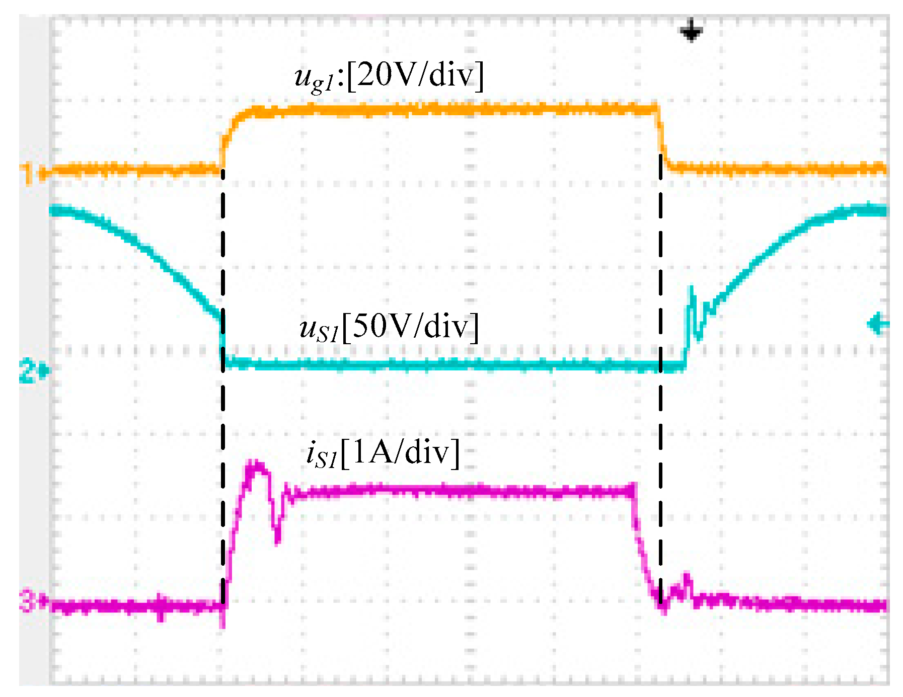
Detailed waveforms of the proposed system are shown in Figure 19. As described in Section 5, the switches turn off in the zero-crossing point of uCp. The overlap time Tov is regulated automatically and the operation conditions are satisfied.
Figure 20 shows waveforms of one switch. During the turn-on time, the current of switch iS equals to 0 and slowly increases, which means ZCS is achieved. At turn-off time, the voltage of the switch uCp remains at zero and ZVS are achieved. Because of these excellent properties, loss of switching devices in the system can be greatly reduced, that is, the efficiency will be enhanced. When the distances of LP and LS increase, the system still operates normally, as shown in Figure 21.
To verify the theoretical model, a set of experimental data was measured. The experimental and theoretical voltage gains are compared in Figure 22.
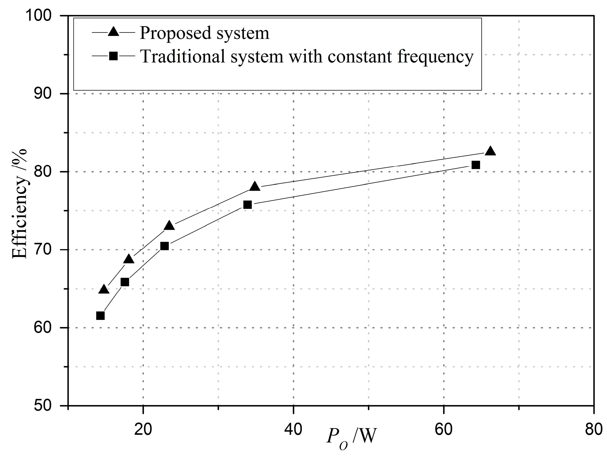
The efficiency of traditional parallel WPT system and new WPT system is compared in Figure 23. During large load variation, efficiency of proposed system is always higher than traditional system due to short current is effectively controlled.
8. Conclusions
Short currents occur in WPT systems when the operation frequency drifts from the inherent frequency of the resonant network. This phenomenon is quite dangerous for switching components and other circuit components. This paper proposes a novel method, named inductance-damping method, based on utilizing an additional small inductance to inhibit short currents. Steady-state mode and operating conditions are analyzed. An overlapping time regulation circuit is given and the range of is discussed. The system design procedure is described and a design example is discussed. The experimental waveforms and data are given to verify the method. Furthermore, this method can be extended to Current-Fed full-resonant converters.
Acknowledgments
The research work is financially supported by the research fund of National Natural Science Foundation of China (Nos. 51377183, 51377187).
Author Contributions
Author Yanling Li implemented the research, performed the analysis, experimental data analysis and wrote the paper. Author Qichang Duan contributed the main idea of this paper and provided guidance and supervision. Author Weiyi Li carried out experimental tests.
Conflicts of Interest
The authors declare no conflict of interest.
References
- Villa, J.L.; Sallan, J.; Osorio, J.F.S.; Llombart, A. High-misalignment tolerant compensation topology for ICPT systems. IEEE Trans. Ind. Electron. 2012, 59, 945–951. [Google Scholar] [CrossRef]
- Zhang, W.; Wong, S.C.; Chi, K.T.; Chen, Q. Design for efficiency optimization and voltage controllability of series—Series compensated inductive power transfer systems. IEEE Trans. Power Electron. 2014, 29, 191–200. [Google Scholar] [CrossRef]
- Pantic, Z.; Lukic, S.M. Framework and topology for active tuning of parallel compensated receivers in power transfer systems. IEEE Trans. Power Electron. 2012, 27, 4503–4513. [Google Scholar] [CrossRef]
- Thrimawithana, D.J.; Madawala, U.K. A generalized steady-state model for bidirectional IPT systems. IEEE Trans. Power Electron. 2013, 28, 4681–4689. [Google Scholar] [CrossRef]
- Huang, C.Y.; Boys, J.T.; Covic, G.A. LCL pickup circulating current controller for inductive power transfer systems. IEEE Trans. Power Electron. 2013, 28, 2081–2093. [Google Scholar] [CrossRef]
- Madawala, U.K.; Neath, M.; Thrimawithana, D.J. A power–frequency controller for bidirectional inductive power transfer systems. IEEE Trans. Ind. Electron. 2013, 60, 310–317. [Google Scholar] [CrossRef]
- Chen, R.Y.; Liang, T.J.; Chen, J.F.; Lin, R.L.; Tseng, K.C. Study and implementation of a current-fed full-bridge boost DC—DC converter with zero-current switching for high-voltage applications. IEEE Trans. Ind. Appl. 2008, 44, 1218–1226. [Google Scholar] [CrossRef]
- Yuan, B.; Yang, X.; Zeng, X.; Duan, J.; Zhai, J.; Li, D. Analysis and design of a high step-up current-fed multiresonant DC–DC converter with low circulating energy and zero-current switching for all active switches. IEEE Trans. Ind. Electron. 2012, 59, 964–978. [Google Scholar] [CrossRef]
- Hu, A.P. Selected Resonant Converters for IPT Power Supplies. Ph.D. Thesis, Department of Electrical and Computer Engineering, Auckland University, Auckland, New Zealand, 2001. [Google Scholar]
- Si, P.; Hu, A.P.; Malpas, S.; Budgett, D. A frequency control method for regulating wireless power to implantable devices. IEEE Trans. Biomed. Circuits Syst. 2008, 2, 22–29. [Google Scholar] [CrossRef] [PubMed]
- Hu, A.P.; Boys, J.T.; Covic, G.A. Frequency analysis and computation of a current-fed resonant converter for ICPT power supplies. In Proceedings of the International Conference on Power System Technology, Perth, Australia, 4–7 December 2000; pp. 327–332. [Google Scholar]
- Tang, C.S.; Sun, Y.; Su, Y.G.; Nguang, S.K.; Hu, A.P. Determining multiple steady-state ZCS operating points of a switch-mode contactless power transfer system. IEEE Trans. Power Electron. 2015, 24, 416–425. [Google Scholar] [CrossRef]
- Su, Y.G.; Zhang, H.Y.; Wang, Z.H.; Hu, A.P. Steady-state load identification method of inductive power transfer system based on switching capacitors. IEEE Trans. Power Electron. 2015, 30, 6349–6355. [Google Scholar] [CrossRef]
- Wang, Z.H.; Li, Y.P.; Sun, Y.; Tang, C.S.; Lv, X. Load detection model of voltage-fed inductive power transfer system. IEEE Trans. Power Electron. 2013, 28, 5233–5243. [Google Scholar] [CrossRef]
- Hu, A.P.; Covic, G.A.; Boys, J.T. Direct ZVS start-up of a current-fed resonant inverter. IEEE Trans. Power Electron. 2006, 21, 809–812. [Google Scholar] [CrossRef]
- Dai, X.; Sun, Y. An accurate frequency tracking method based on short current detection for inductive power transfer system. IEEE Trans. Ind. Electron. 2014, 61, 776–783. [Google Scholar] [CrossRef]
- Namadmalan, A. Bidirectional current-fed resonant Inverter for contactless energy transfer systems. IEEE Trans. Ind. Electron. 2015, 62, 238–245. [Google Scholar] [CrossRef]
- Yan, K.; Chen, Q.; Hou, J.; Ren, X.; Ruan, X. Self-oscillating contactless resonant converter with phase detection contactless current transformer. IEEE Trans. Power Electron. 2014, 29, 4438–4449. [Google Scholar] [CrossRef]
- Forsyth, A.J.; Ward, G.A.; Mollov, S.V. Extended fundamental frequency analysis of the LCC resonant converter. IEEE Trans. Power Electron. 2003, 18, 1286–1292. [Google Scholar] [CrossRef]
Figure 1.
Current-Fed WPT system.

Figure 2.
The general topology that can generate short currents.

Figure 3.
Waveform and circuit when equals to .

Figure 4.
Short current analysis in a Current-Fed IPT system: (a) Capacitive case, ; (b) Inductive case, .
Figure 4.
Short current analysis in a Current-Fed IPT system: (a) Capacitive case, ; (b) Inductive case, .
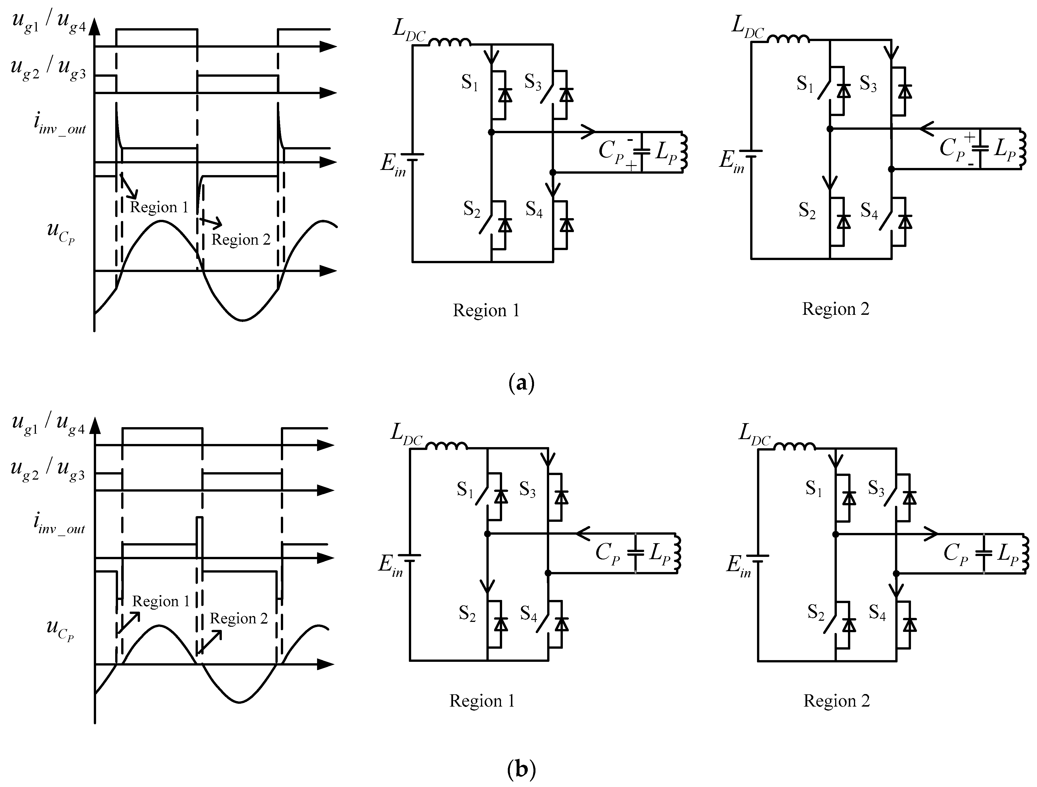
Figure 5.
Current-Fed WPT system using the proposed inductance-damping method.
Figure 6.
Steady-state waveform of the proposed system in a cycle.
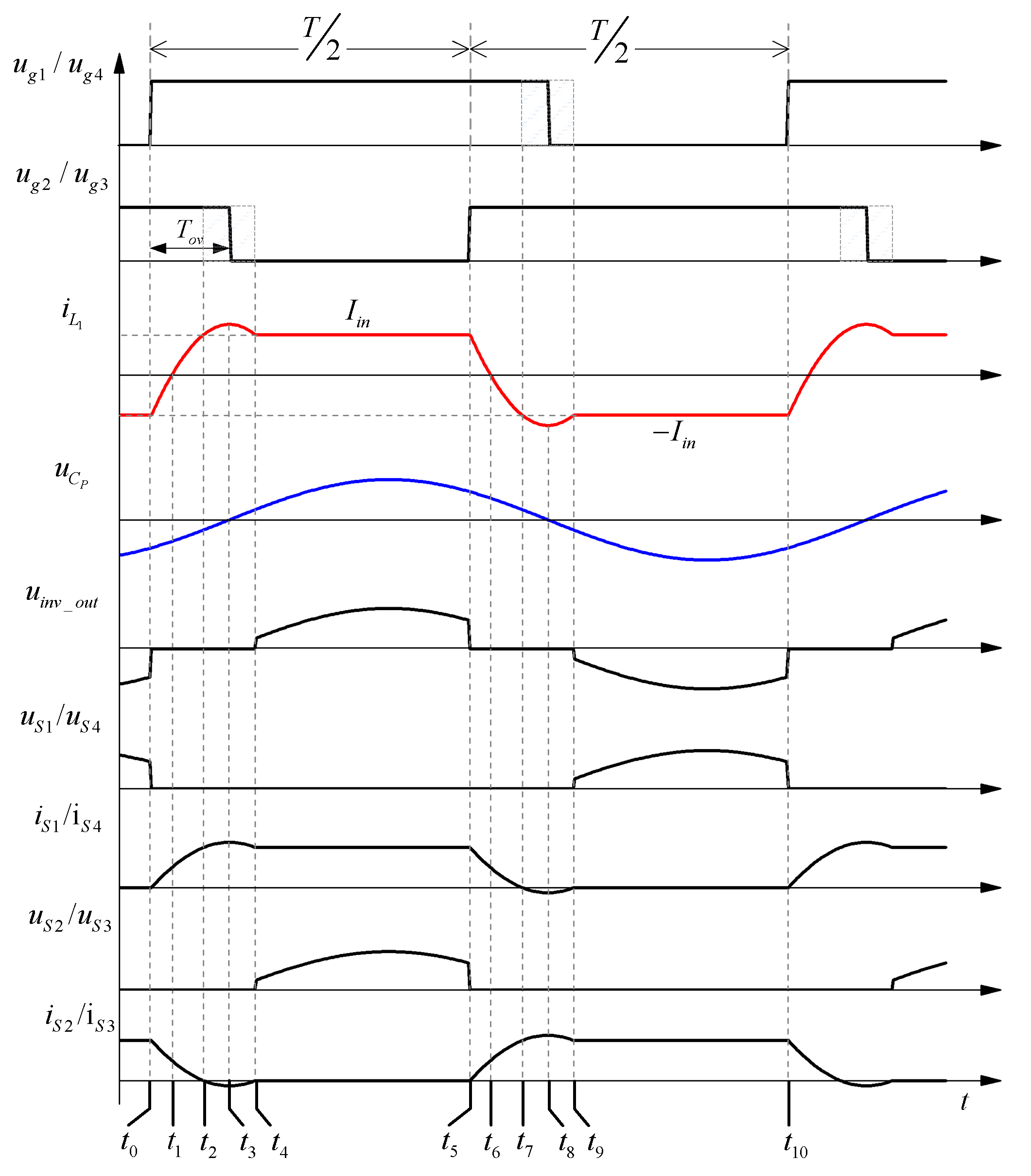
Figure 7.
Operating modes of the proposed system: (a) Mode 0 [Before ]; (b) Mode 1 []; (c) Mode 2 [].
Figure 7.
Operating modes of the proposed system: (a) Mode 0 [Before ]; (b) Mode 1 []; (c) Mode 2 [].

Figure 8.
Equivalent circuit for steady-state analysis.
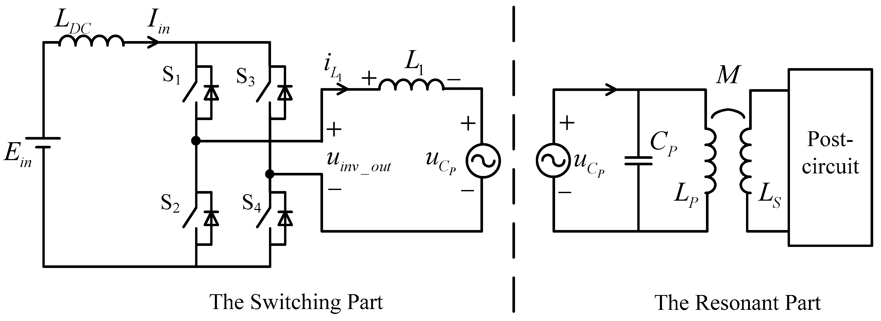
Figure 9.
Waveform when is too large.
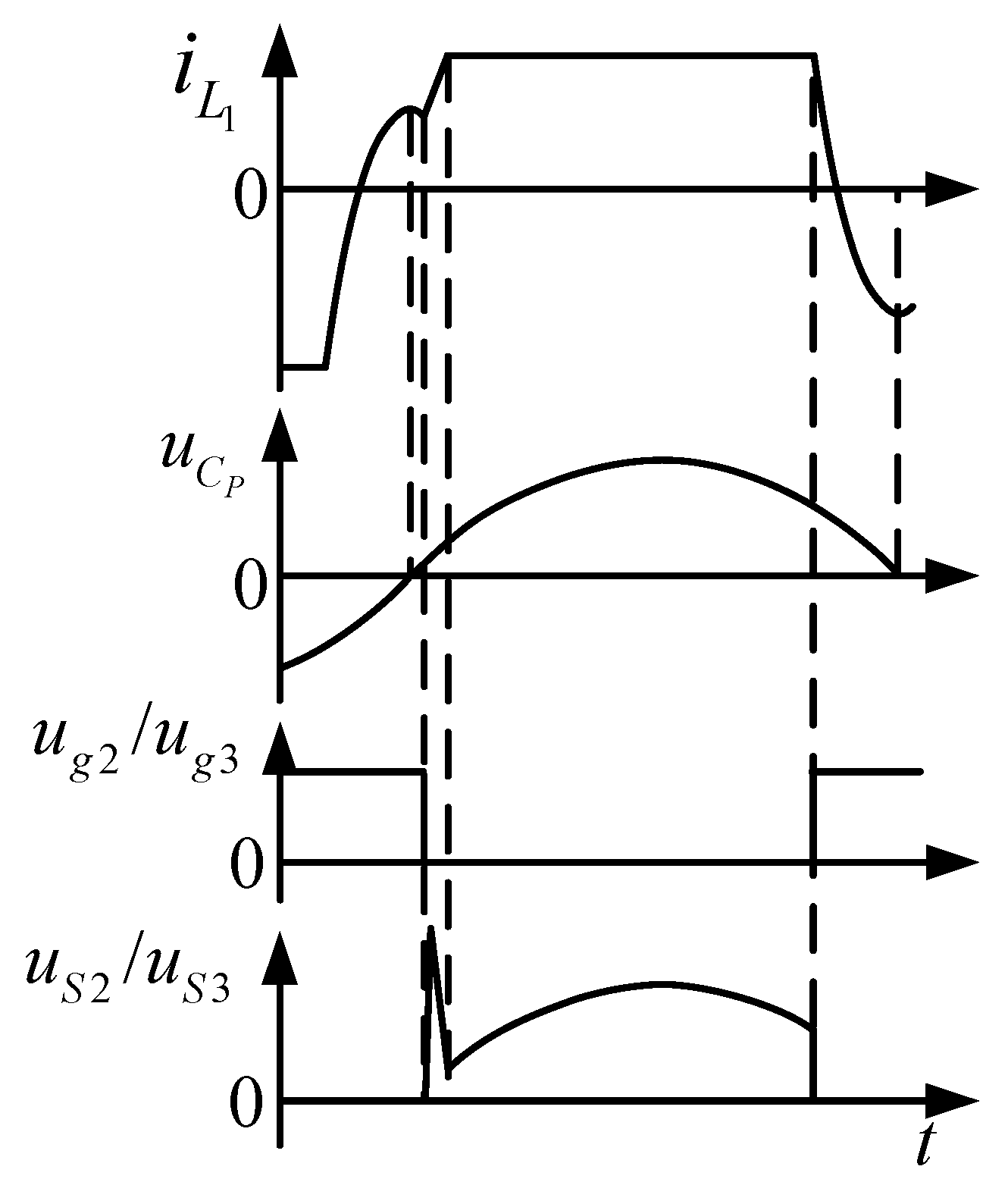
Figure 10.
Schematic diagram of overlapping-time self-regulating circuit.
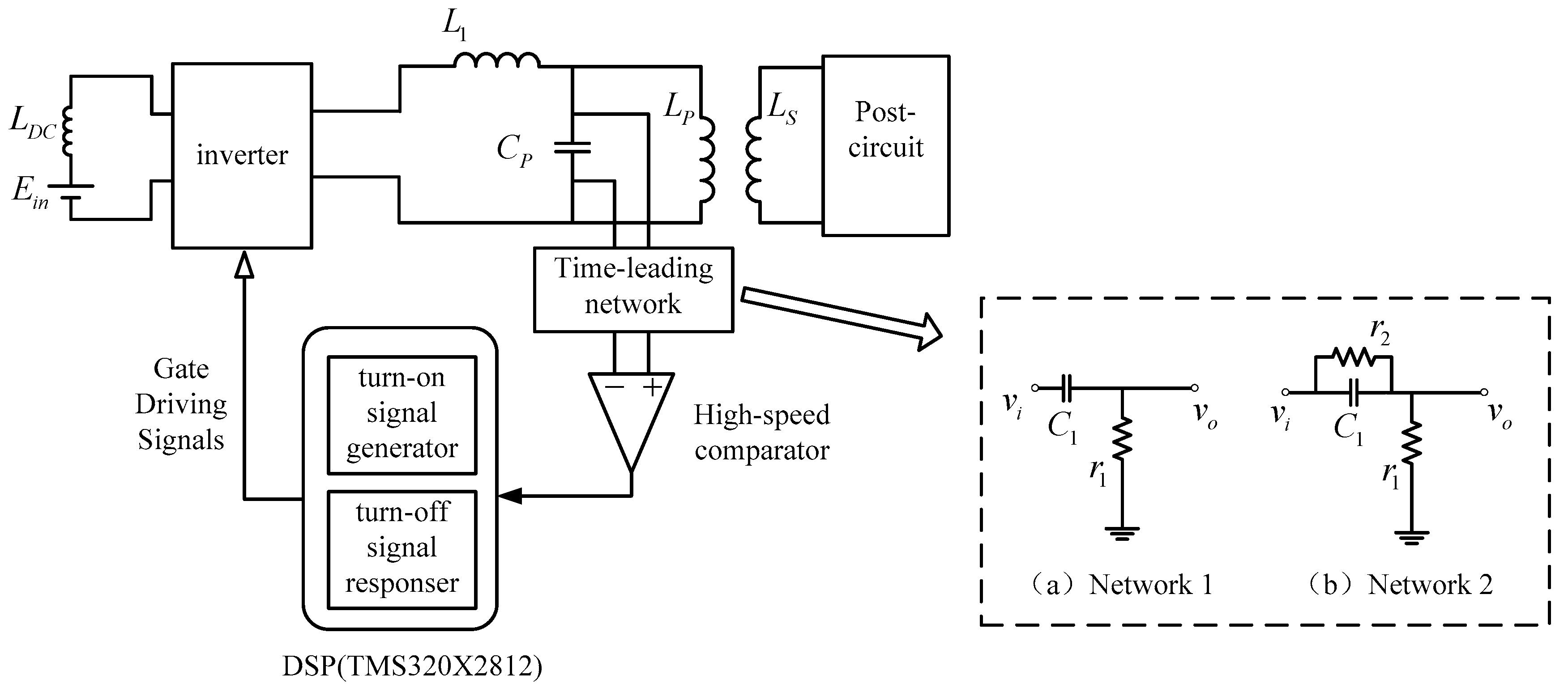
Figure 11.
Waveform in the critical mode.
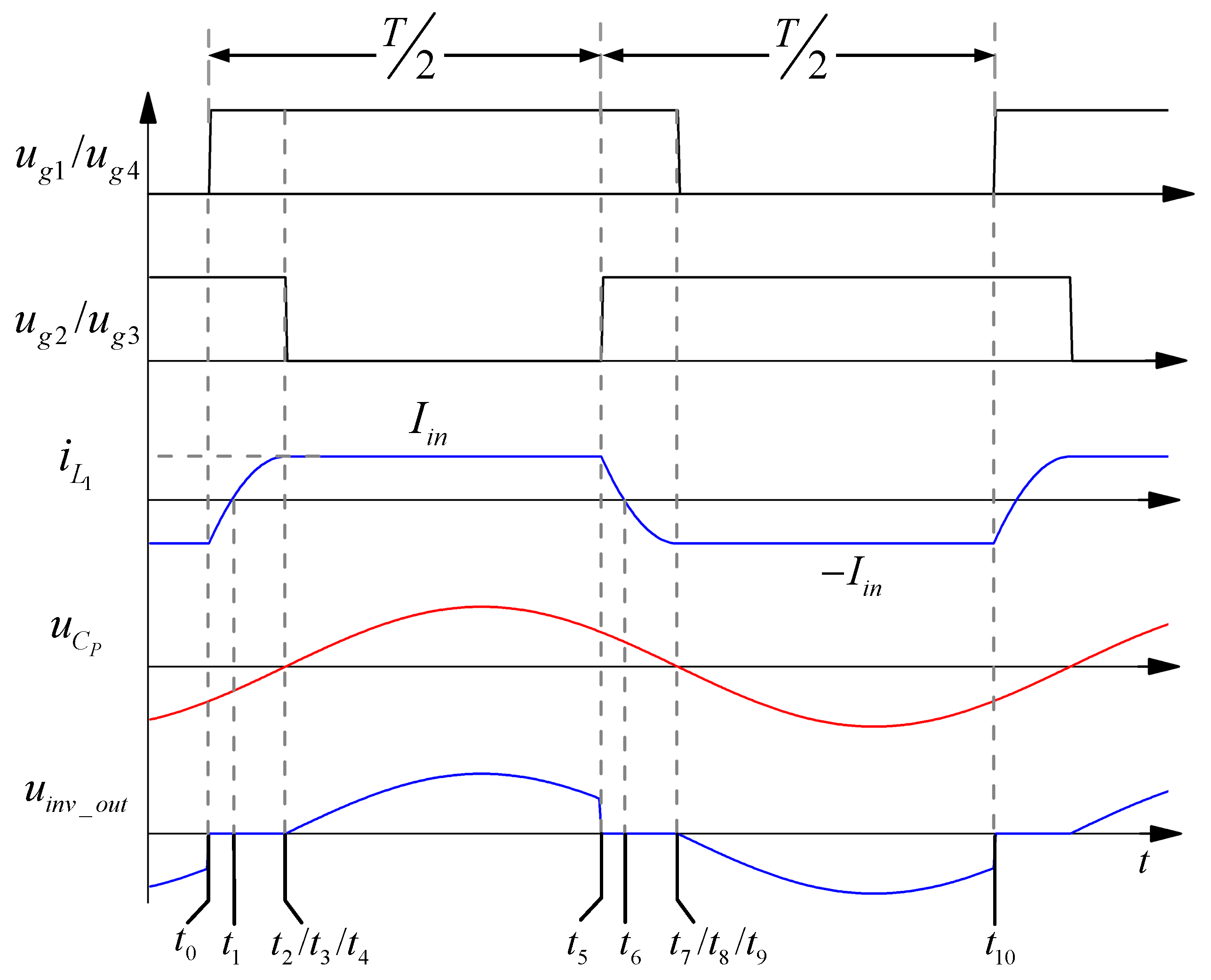
Figure 12.
Design flowchart.

Figure 13.
Circuit of the experimental system (with series resonant network in secondary side).

Figure 14.
Relationship between Angle[Zin] and operating frequency of the experimental system: (a) RL varies, M = 11.53 μH; (b) M varies, RL = 10 Ω.
Figure 14.
Relationship between Angle[Zin] and operating frequency of the experimental system: (a) RL varies, M = 11.53 μH; (b) M varies, RL = 10 Ω.

Figure 15.
The critical value L1_cri: (a) RL varies, M = 11.53 μH; (b) M varies, RL = 10 Ω.
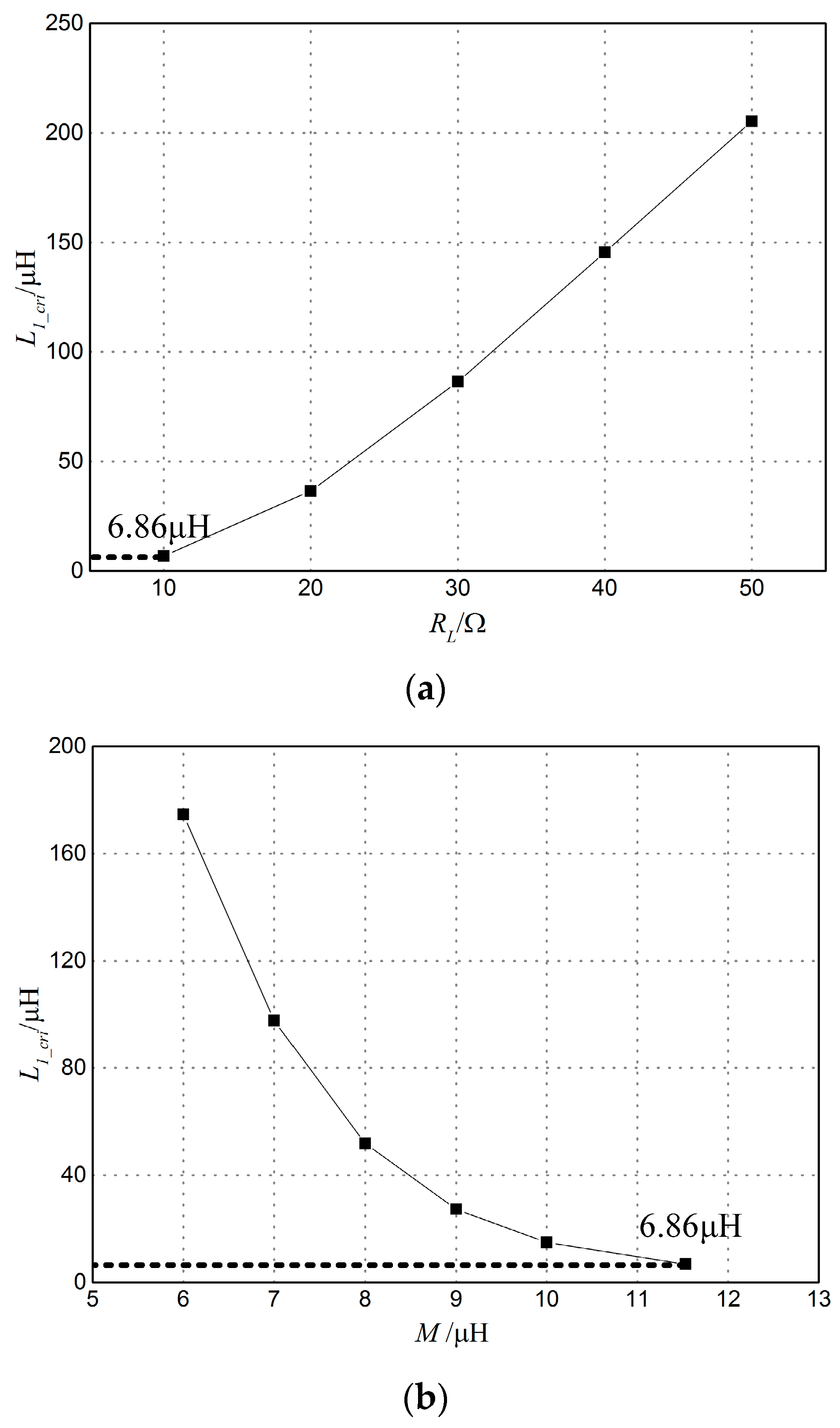
Figure 16.
Photo of the prototype.

Figure 17.
The coupling structure.
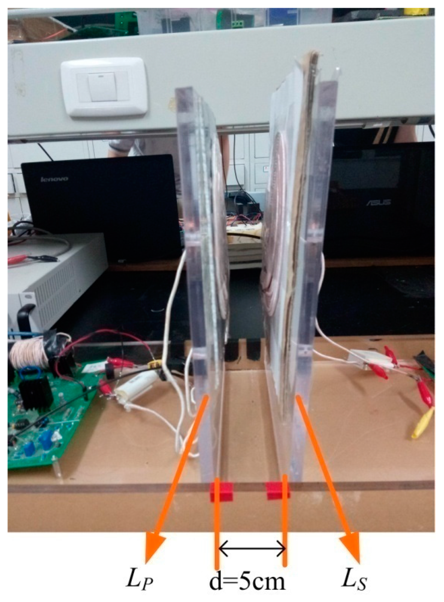
Figure 18.
Short current control performance comparison: (a) Traditional parallel WPT system under heavy load condition ( = 10 Ω); (b) Short current control performance with = 3.45 µH, = 10 Ω; (c) Short current control performance with = 6.40 µH, = 10 Ω.
Figure 18.
Short current control performance comparison: (a) Traditional parallel WPT system under heavy load condition ( = 10 Ω); (b) Short current control performance with = 3.45 µH, = 10 Ω; (c) Short current control performance with = 6.40 µH, = 10 Ω.
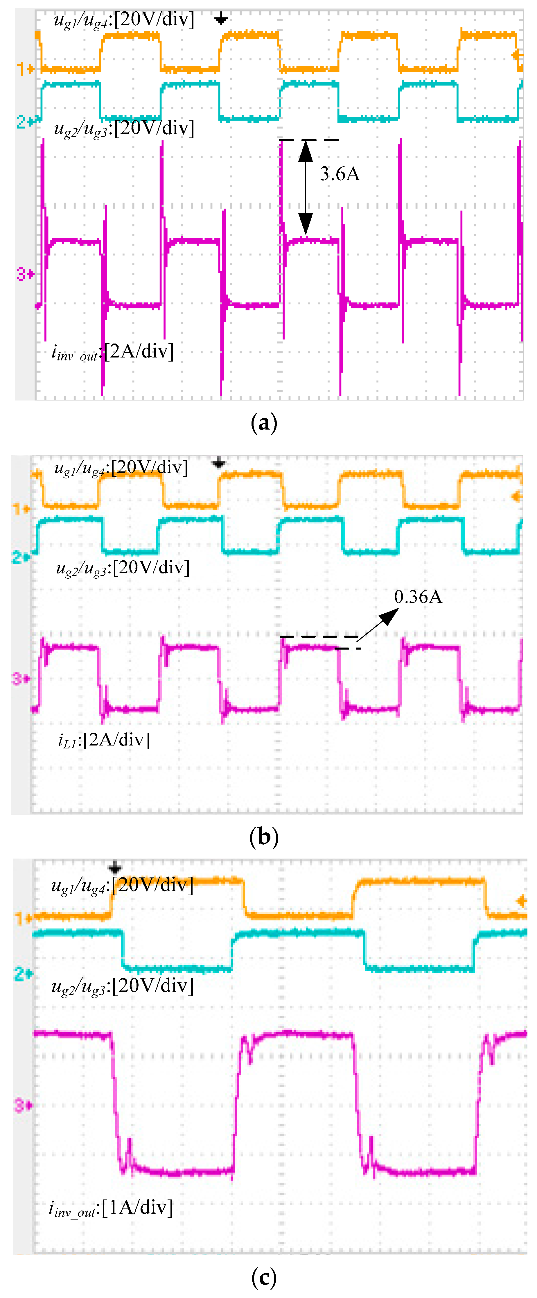
Figure 19.
The switching waveform during the commutation period (when = 10 Ω, = 3.45 µH).

Figure 20.
Waveform of switch (when = 10 Ω, = 3.45 µH).

Figure 21.
Steady-state waveform when M varies ( = 10 Ω, = 3.45 µH): (a) 6 cm, M = 8.77 µH; (b) 7 cm, M = 6.70 µH.
Figure 21.
Steady-state waveform when M varies ( = 10 Ω, = 3.45 µH): (a) 6 cm, M = 8.77 µH; (b) 7 cm, M = 6.70 µH.
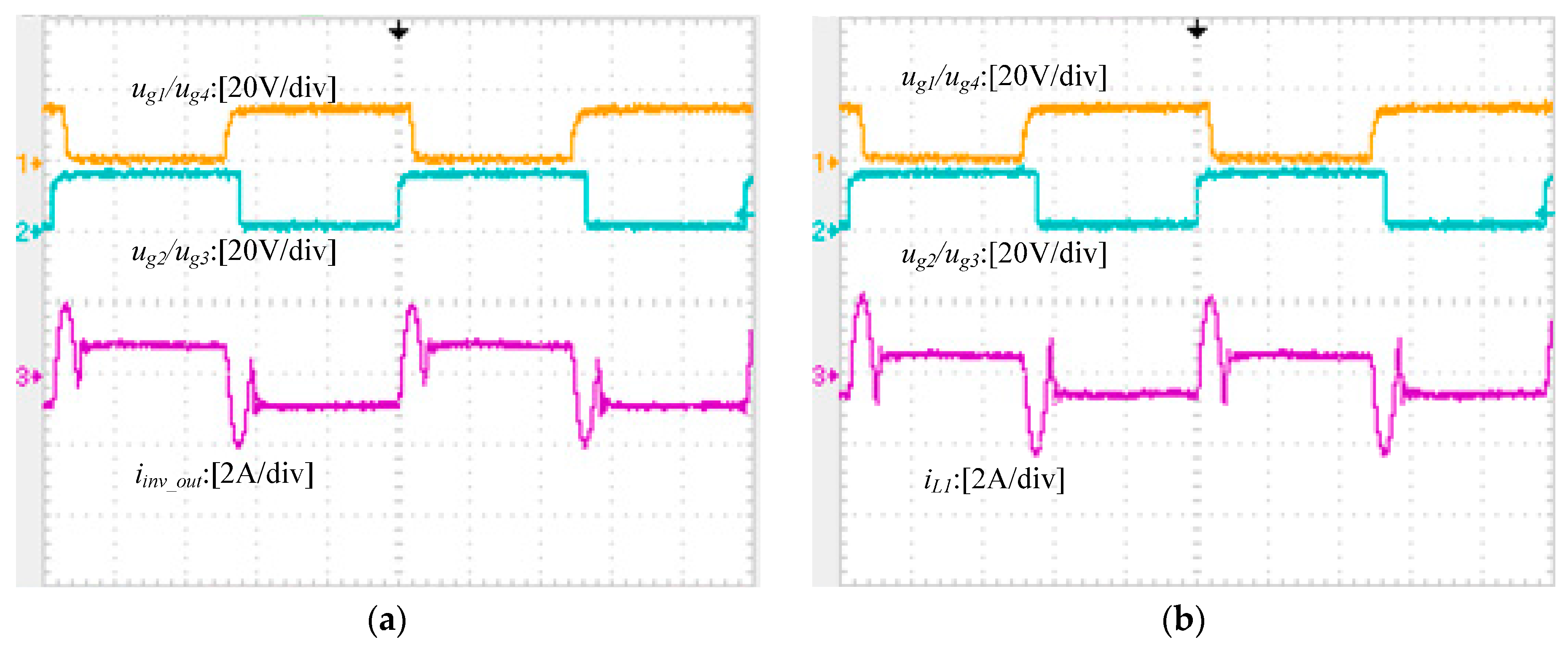
Figure 22.
Comparison of theoretical value and experimental data of .
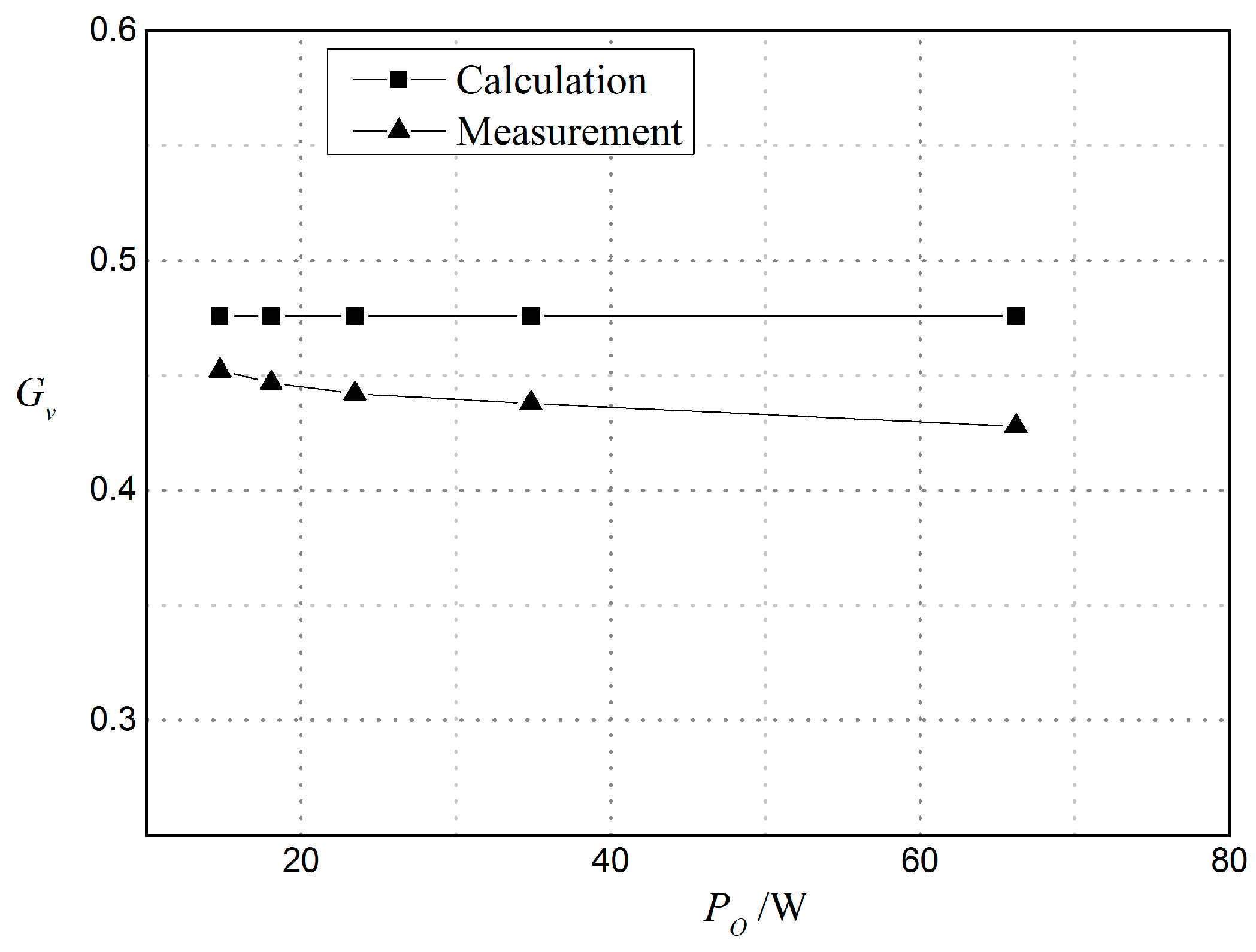
Figure 23.
Efficiency of traditional system and proposed system.

Table 1.
Parameters of the experimental system.
| Parameter | Value |
|---|---|
| Ein | 60 V |
| LDC | 2.23 mH |
| RLDC | 0.19 Ω |
| LP | 29.89 µH |
| RLP | 0.058 Ω |
| CP | 0.528 µF |
| M | 11.53 µH (rated) |
| LS | 60.59 µH |
| RLS | 0.093 Ω |
| CS | 0.37 µF |
| CO | 220 µF |
| RL | 10 Ω (rated) |
© 2017 by the authors. Licensee MDPI, Basel, Switzerland. This article is an open access article distributed under the terms and conditions of the Creative Commons Attribution (CC BY) license (http://creativecommons.org/licenses/by/4.0/).
Share and Cite
MDPI and ACS Style
Li, Y.; Duan, Q.; Li, W. A Short-Current Control Method for Constant Frequency Current-Fed Wireless Power Transfer Systems. Energies 2017, 10, 585. https://doi.org/10.3390/en10050585
AMA Style
Li Y, Duan Q, Li W. A Short-Current Control Method for Constant Frequency Current-Fed Wireless Power Transfer Systems. Energies. 2017; 10(5):585. https://doi.org/10.3390/en10050585
Chicago/Turabian StyleLi, Yanling, Qichang Duan, and Weiyi Li. 2017. "A Short-Current Control Method for Constant Frequency Current-Fed Wireless Power Transfer Systems" Energies 10, no. 5: 585. https://doi.org/10.3390/en10050585
Note that from the first issue of 2016, this journal uses article numbers instead of page numbers. See further details here.