
Control Strategy of Single-Phase Three Level Neutral Point Clamped Cascaded Rectifier


School of Electrical Engineering, Southwest Jiaotong University, Chengdu 610031, China
*
Author to whom correspondence should be addressed.
Energies 2017, 10(5), 592; https://doi.org/10.3390/en10050592
Submission received: 20 March 2017
/
Revised: 21 April 2017
/
Accepted: 22 April 2017
/
Published: 28 April 2017
(This article belongs to the Special Issue Power Electronics in Power Quality)
Abstract
:Single-phase 3-level neutral point clamped cascaded rectifier (3LNPC-CR) has been successfully made its way into traction drive system as a high-voltage traction converter. In this passage, the control issue of the 3LNPC-CR is considered. A transient current control strategy, combined with proportional integral (PI) controllers, is adopted to achieve unity power factor, satisfactory sinusoidal grid current, regulated overall dc voltage, and even efficient voltage balance between each module. Besides, with regard to the instinct voltage fluctuation problem among dc-link capacitors in one 3-level neutral point clamped (3LNPC) rectifier module, a phase shift carrier space vector pulse width modulation (PSC-SVPWM) worked along with a reasonable redundancy selection scheme is addressed. In addition, two auxiliary balancing circuits for a single-phase 3LNPC rectifier is proposed. The voltage balancing capacity of these internal-module balancing schemes are analyzed and compared. Finally, the control performance of these proposed strategies are verified by simulations and experiments.
1. Introduction
Multilevel converters have successfully made their way into the high-power application area and are considered to be a proven technology [1,2]. By increasing the number of modules connected in a series, it is possible to generate more voltage levels to synthesize the input terminal voltage, which makes the voltage and current harmonics significantly decrease [3,4]. The cascaded multilevel converter has received increased attention due to its advantages over other topologies. Firstly, the series rectifiers are able to share the overall input voltage, featuring power semiconductors with a lower voltage rating [5]. Thus, with more modules connected in series, the voltage that applied at the converter terminals could be higher. Secondly, a proper choice of the electronic components and the number of cascaded modules allows removing of the heavy, bulky and expensive step-down transformer [6,7,8,9]. Last but not least, cascaded multilevel converters feature high modularity degree that makes it possible to operate the converter even under faulty conditions by immediately replacing the faulty module [10]. In this way, the reliability of this system is increased. A Hani Packed U-cell (HPUC) is introduced to generate a multi-level voltage waveform at the input in [11]. Moreover, a single-phase Three level neutral point clamped cascaded rectifier (3LNPC-CR) is hired due to its ability to deal with the high voltage in traction power system [12].
In order to properly operate a cascaded converter with n modules connected in series, the control of the grid current and the respective dc-link voltages are necessary [13]. In fact, each module must interact with the others to obtain a regulated grid current, notwithstanding all of the modules transfer power independently. In addition, the dc-link loads of each module may be different. However, the voltage on each dc-link load has to be equalized and stabilized even if the loads are unequal. In order to equalize the output voltages of the dc-terminals, the redundancy-based voltage balancing scenarios are presented [14]. In [15], a PI-based balancing control strategy is achieved. Besides, an improved PI-based balancing strategy is adopted as the multi-module voltage balancing strategy [16].
As the number of separate modules increases, the complexity arises for the necessity of the voltage regulation across these dc-links. In comparison with the traditional H-bridge rectifier, the 3LNPC rectifier generates more voltage levels [17]. In this paper, 3LNPC rectifiers are connected in series to obtain a staircase waveform, which allows for the number of cascaded modules to be decreased [18]. Besides, the demerits of 3LNPC converters cannot be neglected. The neutral-point voltage fluctuation is an urgent problem requiring solution. Inductor-based auxiliary circuit and capacitor-based auxiliary circuit [19,20] are able to extend the stable area and avoid neutral-point voltage fluctuation. However, both of them will cause additional hardware cost. Software based balancing strategy is a more cost-effective way that also manages to balance the dc-link capacitor voltages without installing any additional hardware. An algorithm adjusts the charging/discharging status of dc-link capacitors by selecting redundant [21]. Another algorithm includes regulating on-times of the redundant vectors is presented in [22]. These software-based strategies demonstrate efficient voltage balancing ability and have been applied to single-phase 3LNPC converter.
The main analysis has been focused on the control issue of the 3LNPC-CR. Normally, these control strategies are to fulfill a quadruple task.
- To obtain sinusoidal grid current;
- To achieve unity power factor;
- To regulate and equalize voltages across the output terminals;
- To balance the dc-link capacitor voltages in each module.
Each of these tasks corresponds with one of the common problems in the 3LNPC-CR. The first task is to avoid problems arouse by distorted currents and erroneous failure detection. Completion of the second task allows much lower reactive power requirements. The third task aims to enhance the stability of this system. Besides, the last ensures normal operation of all the 3LNPC rectifiers [23,24].
In this paper, an overall control strategy combined with a PI-based multi-module balancing scheme is proposed to control one grid current plus n dc terminal voltages [25]. The reference modulation signal generated by the overall control strategy is added by a factor that depends on the dc-link voltages in each module. The multi-module voltage balance boundaries are analyzed and the results are verified by experiment. With regard to neutral point voltage fluctuation problem in each module, a redundancy-based strategy used along with phase shift carrier space vector pulse width modulation (PSC-SVPWM) and two hardware-based balancing auxiliary circuits, including inductor-based auxiliary circuit and capacitor-based auxiliary circuit, are adopted to balance the voltages across the dc capacitors in each module. The feasibility and effectiveness of the inductor-based auxiliary circuit is validated by simulation and experiment.
This paper is organized as follows. First, the 3LNPC cascaded topology and its working principle is presented in Section 2. Then, the modulation scheme is explained in Section 3. The control strategies are introduced in detail in the fourth section. The last section shows the simulation and experimental results that validate the proper operation of the converter.
2. Topology
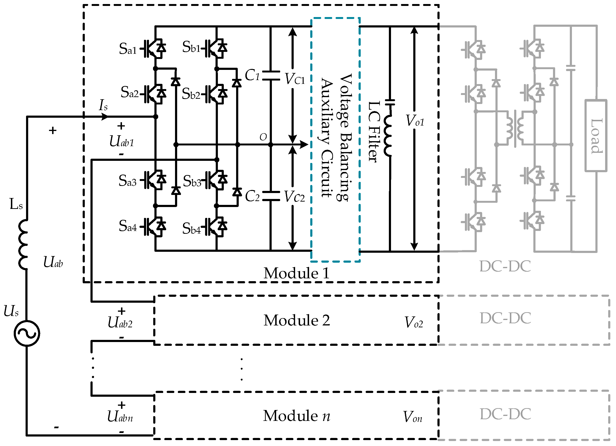
A basic structure of a single phase 3LNPC is illustrated in Figure 1. All the rectifiers with their respective LC filters are connected in series, sharing the common AC voltage source us and the input inductance Ls. The internal-module balancing auxiliary circuit is in parallel connection with the dc-link capacitors within each module.
A single-phase 3LNPC rectifier is composed of two bridge legs Sa and Sb. Each of the bridge leg, made up of IGBTs with antiparallel diodes and clamped diodes, generates three switching states: positive (p), negative (n), or neutral (o). The switching states of bridge leg Sa and Sb are determined by the following relation:
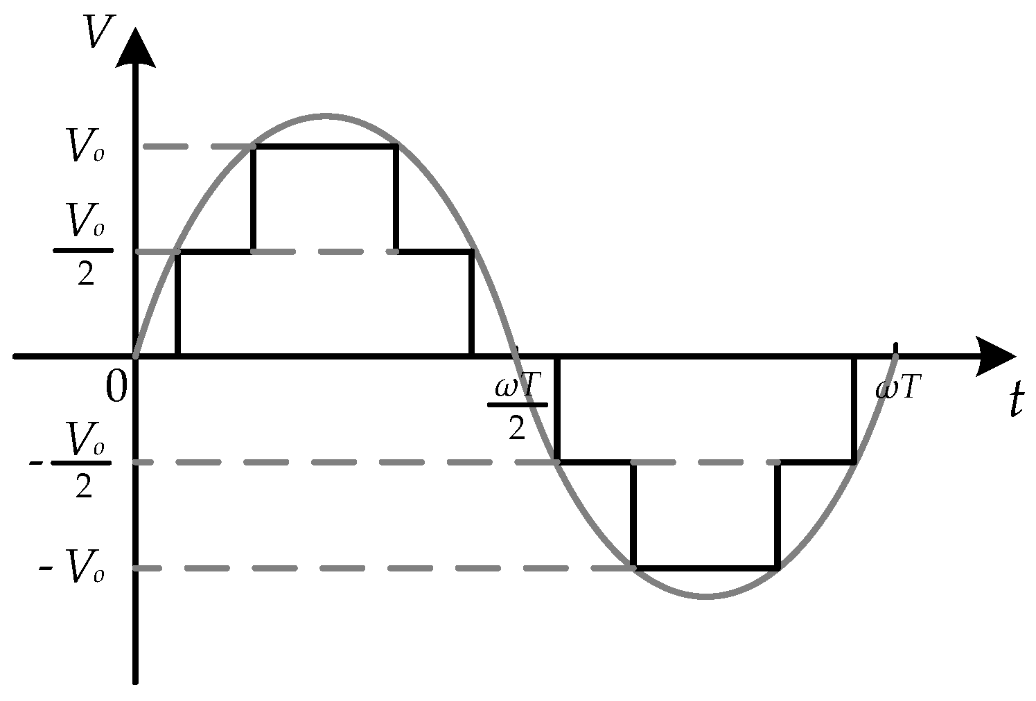
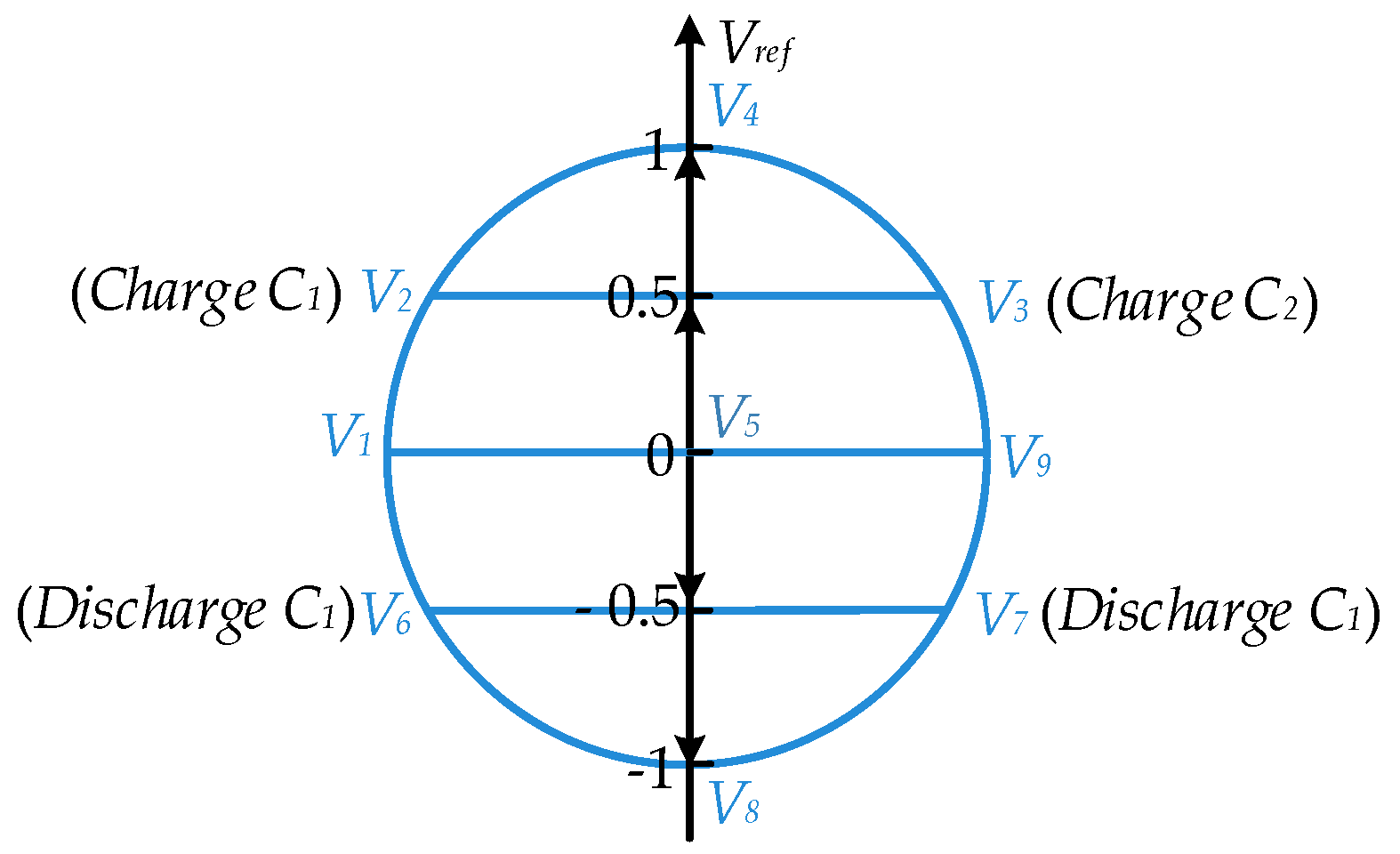
Therefore, the number of total switching states in a single rectifier, contributed by 2 bridge legs, is 9, the square of 3. All available voltage vectors for a single phase 3LNPC rectifier are covered in Table 1. Suppose the voltages on capacitor C1 and C2 are the same and equal to Vo. As shown in Figure 2, these vectors (Vo, Vo/2, 0, −Vo/2, −Vo) represent the input voltage uab with 5 voltage levels.
Taking into account the intrinsic neutral point voltage fluctuation problem, the charging or discharging status of dc-link capacitors while the grid current is is in the positive direction is also covered in Table 1. The dc-link capacitor voltages VC1 and VC2 are assumed to be the same in normal conditions. Thus, as it is described in Table 1, these voltage vectors can be divided into 5 categories according to their effects on the terminal voltage uab:
Zero (Z) vector: V1, V5 and V9. For these vectors, the dc-link capacitors are neither charged nor discharged.
Small positive (SP) vector: V2 and V3. Considering that VC1 equals to VC2 when the internal-module voltage balancing scheme is accomplished, these switching states generate the same terminal voltage (Vo/2). Even though, the charging/discharging status of the dc-link capacitors are different. For V2, the grid current would charge C1 but has no effect on C2, while for V3, the grid current would charge C2 but has no effect on C1.
Large positive (LP) vector: V4. The switching state of this vector is unique. The dc-link capacitors are connected in series, charged by the grid current is via switches Sa1, Sa2, Sb3 and Sb4.
Small negative (SN) vector: V6 and V7. Considering that VC1 equals to VC2 when the internal-module voltage balancing scheme is accomplished, these switching states generate the same terminal voltage (−Vo/2). Even if these two switching states are redundant while the neutral point voltage is balanced, the charging/discharging status are opposite. V6 would discharge C2 but has no effect on C1, while V7 would discharge C1 but has no effect on C2.
Large negative (LN) vector: V8. Opposite to LP vector, Switches Sa3, Sa4, Sb1 and Sb2 are on to provide a discharge loop for dc-link capacitors C1 and C2.
According to the switching states identified before, the input voltage of each module uabi (i = 1, 2,…, n) can be described as follows.
Considering n cells with the same dc-link voltage, 5 voltage levels will be generated by each module and the repeated (n − 1) zero voltages should be removed. That is to say, the rectifier can synthesize an input voltage uab with 5n − (n − 1) levels.
Thus, according to the Kirchhoff laws, the grid-side dynamic behavior of the system can be described as:
3. Modulation Scheme
Among various modulation techniques for a 3LNPC rectifier, SVPWM is an attractive candidate due to the following merits. It has a more explicit physical meaning, and is more suitable for digital signal processor implementation. The modulation wave of module i is represented as uabi* (i = 1, 2, …, n). The modulation waveform for each module is divided into four sectors according to Vref, the instantaneous value of uabi*. That is:
- Sector 1: 0.5 < Vref ≤ 1;
- Sector 2: 0 < Vref ≤ 0.5;
- Sector 3: −0.5 ≤ Vref < 0;
- Sector 4: −1 < Vref ≤ −0.5.
The space vector diagram made up of four sectors is shown in Figure 3. Each borderline of these four sectors corresponds with certain voltage vectors discussed above. The selection of the switching state is determined only after identifying the sector, in which the modulation wave works. The reference vector Vref can be composed by the two nearest voltage vectors Va and Vb. For example, when the modulation wave works in the sector 1, the reference vector Vref is composed by V4 and V2 (or V3). Since V2 and V3 are redundant to each other, either of them has a chance to be adopted, and both of them working alone with V4 will be able to generate the same reference vector. However, the selection of V2 or V3 will affect the balance between the dc-link capacitor voltages, which will be discussed in next section.
On-time calculation is based on the volt-second balance equation and time balance equation.
Va and Vb are the voltage vectors selected to synthesis the reference voltage vector Vref, correspondingly, Ta and Tb stands for the duty time of the relevant voltage vector. Since the choice of voltage vectors varies in different sector, the on-time calculation results change with the position of the reference vector. Since the redundant vectors will produce different charging/discharging status of the dc-link capacitors. It is obvious that the SP and SN vector could be the main reason for the neutral-point fluctuation problem. The redundant vectors in SP and SN vector categories have different effects on the dc-link capacitors. Hence, the performance of the internal-module voltage balancing scheme significantly depends on the selection of these switching states.
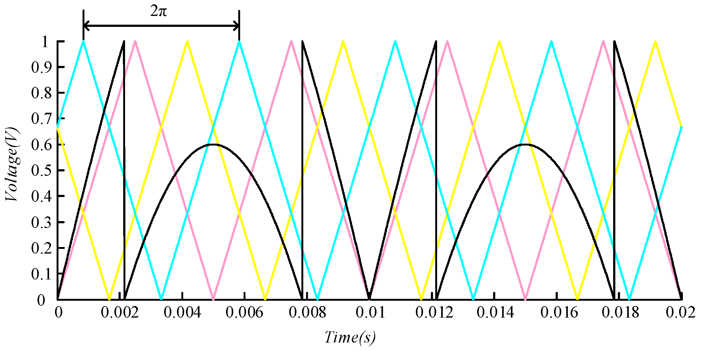
In this paper, an extension of the single phase 3LNPC rectifier SVPWM technique is adopted in cascaded multilevel rectifier. The harmonic content of the output voltage waveform can be reduced by shifting the relative phases of the triangular carrier employed in each NPC rectifier. For a cascaded rectifier with 3 power cells, the carrier waves between adjacent cells have a phase-angle difference of 2π/3 as shown in Figure 4. So that the three-module 3LNPC-CR have thirteen voltage levels to reduce the voltage stress and harmonic contents.
4. Balancing Strategy
In contrast to its advantageous modularity, each module of the cascaded multilevel rectifier cannot be considered as a separate structure to control. The main difficulties of implementing the single phase 3LNPC-CR concentrate on its control algorithm.
4.1. Overall Control
In fact, n rectifiers have to be regulated through the same AC current. Thus, the sum of the dc-terminal voltages could be considered as an overall output voltage uo,sum. In order to obtain the grid-side unity power factor and a dc-side satisfactory load voltage regulation, the transient current control is adopted. The basic structure of the proposed scheme is depicted in Figure 5. The control scheme includes 2 loops: a current loop and a voltage loop. The current loop is adopted to improve the dynamic response of system and is necessary for generating a sinusoidal input current with unity power factor. A phase locked loop is adopted to lock the voltage phase and, in addition, to generate the synchronized outputs. By multiplying a reference input current amplitude Is* with the sinusoidal signal in phase with the grid voltage, a suitable instantaneous reference grid current is* is obtained. The error between is* and is is sent to the Proportional (P) current controller. In this case, a satisfactory grid current, who takes the path of the input voltage could be reached. The reference amplitude of the input current is derived from the voltage loop. A controller is employed in the outer control loop to maintain the dc-link overall voltage uo,sum at the desired reference value uo,sum*. The error of the dc-link overall voltage is controlled through a Proportional Integral (PI) voltage controller. The output value of the PI voltage controller is chosen as the amplitude of the reference gird current amplitude Is*. Finally, the output of the overall controller, which is supposed to work as the overall modulation signal uab*, is given by the grid side KVL equation.
4.2. Mutual-Module Voltage Balancing Strategy
Cascaded multilevel converter aims to establish equal dc voltages across the dc terminals, which can become difficult if the loads attached to each module are not equal, or the series rectifiers have various characters. A PI-based solution is presented for voltage balancing of distinct dc terminals in cascaded multilevel rectifier to prevent the mutual-model voltage fluctuation.
The mutual-module voltage balancing scheme is addressed to ensure that the respective dc-side voltage uoi of module i (i = 1, 2, …, n) converge to the respective reference value uoi*. As illustrated in Figure 6. This PI-based voltage balancing scheme is basically adjust the modulation waves for each module. The output voltage of each module uoi is compared with the reference voltage uoi*. The error between uoi and uoi* is sent into a PI regulator to derive the amplitude of the compensating current. In order to obtain the simultaneous grid current error (∆ei), the output of each PI controller is multiplied with a unit sinusoidal signal in phase with the grid voltage. The modulation signals of each module uabi* are derived from the sum of corresponding grid current error (∆ei) and the overall modulation signal (uab*). Therefore, the modulation wave in each module is adjusted so that the real power distribution can be changed according to the instantaneous output voltage. For the module with a lower output voltage, the real power transmitted to this module will be increased. In addition, the real power transmitted to the module with a higher output voltage will be decreased. In this way, the output voltages of all the cascaded modules can be balanced.
According to the definition, the modulation depth of each module shows the connection between the peak value of the input voltage and the output voltage in each module. As shown in the following equation, mi represents the modulation depth of module i (i = 1, 2, …, n).
The input inductance is neglected since it has little effect on input voltage. Thus, the effective value of the grid voltage is represented as:
M equals to the modulation depth of a 3LNPC-CR with n modules. Thus, the relationship between mi and M could be derived as
After the load change, suppose the load of module 1 has the minimum admittance y1 and the loads of the rest modules are of the same admittance value, which could be described as:
The real power transmitted to each module should be proportional to its load admittance. Without the mutual-module balancing scheme, the load with a smaller admittance has a higher voltage while the loads with larger admittance have lower voltage. This change will be reflected in the modulation waveforms of each module. Under the effect of mutual-module balancing scheme, the power transmitted to each module is correspondingly changed. The real power transmitted to the module with a higher voltage will be linearly decreased and the real power transmitted to the module with lower voltage will be linearly increased. In this way, the output voltages of the dc-link terminals will be balanced. However, under the condition of over-modulation, the operation of the modulator will be extended into non-linear regions and will cause significant low-frequency harmonic components. Thus, the balancing strategy will manage to maintain the output voltages only if the modulation depth of each module is between 0 and 1. Otherwise, the change of input power will not be enough to compensate the voltage rise or drop.
The modulation depth of module 2 to module n can be represented by the modulation depth of module 1, as shown in Formula (11).
As mentioned above, in order to maintain the dc-link voltage balanced, the modulation depth of each module is limited between 0 and 1. When the loads of each module are unbalanced, only one circumstance is considered. As derived in Formula (9), the load in module 1 is the only load different from the others. Suppose is of the minimum load admittance, when the loads are unbalanced, the unbalance degree is defined as:
When the loads are balanced, the unbalance degree (∆) equals to 1. When the load of module 1 is cut off, the unbalance degree (∆) equals to 0. Suppose the power losses on the transmission circuit is neglected, the input real power transmitted to module 1 is:
Thus, the modulation depth of module 1 is derived as:
Suppose there is no real power loss during the transmission process, the total input power of the cascaded 3LNPC-CR can be represented as:
Thus, the grid current can be yield as:
Substitute the Is in (14) with (16), the modulation depth of module 1 can be described as:
Substitute the m1 in (11) with (18), the modulation depth of module 2 to module n is derived as:
Combine the Formula (18) with the modulation depth limitation shown in Formula (10), the boundary of unbalance degree is derived:
4.3. Internal-Module Voltage Balancing Strategy
To eliminate the neutral-point voltage fluctuation in each module, several methods, including balancing scheme based on software and hardware, have been proposed.
Software-based balancing scheme reallocates the redundant switching states to eliminate the fluctuation of the neutral-point voltage in each module. This voltage balancing scheme should be used along with the SVPWM. As mentioned above, the SVPWM is achieved only after these following steps:
- Determining the location of the reference signal;
- The calculation of on-times;
- Determination and selection of redundant vectors.
The redundant vectors have different effects on the dc-link capacitors. Thus, by suitably selecting and executing the redundant vectors during respective on-times, VC1 and VC2 could be balanced by adjusting the charging/discharging status of each dc-link capacitors. Power flow signal, worked as a redundancy selection signal, is vital to this process. The voltage difference between dc-link capacitors C1 and C2, along with the grid current are measured to derive a power flow signal. Therefore, the redundant switching states chosen according to the power flow signal are listed in Table 2.
Two kinds of voltage balancing auxiliary circuits, including one based on inductor and the other based on capacitor, are addressed as hardware-based balancing scheme.
The balancing operation based on the additional capacitor Ca1 is described in Figure 7. When Sa1, Sa3 are turned on and Sa2, Sa4 are turned off, energy will exchange between the upper capacitor C1 and the additional capacitor Ca1 via the path highlighted in Figure 7a. C1 charges Ca1 or Ca1 charges C1 when vC1 > vCa1 or vC1 < vCa1. If Sa1, Sa3 are off and Sa2, Sa4 are on, the energy exchange happens between the lower capacitor Ca2 and the additional capacitor Ca1 via the current path highlighted in Figure 7b. In this case, C2 charges Ca1 if vC2 > vCa1 or Ca1 charge C2 while vC2 < vCa1. Therefore the additional Ca1 is important to temporarily store electric power between C1 and C2. A resistor is connected in series with the additional capacitor Ca1 to limit the magnitude of the charge/discharge current. However, compared to its merits of limiting the rush current, the extra resistor will result in unexpected power loss. In order to avoid the short circuit fault, switch Sa1, Sa3 and switch Sa2, Sa4 should be alternately turned on. Finally, the voltages on C1 and C2 will be equalized.
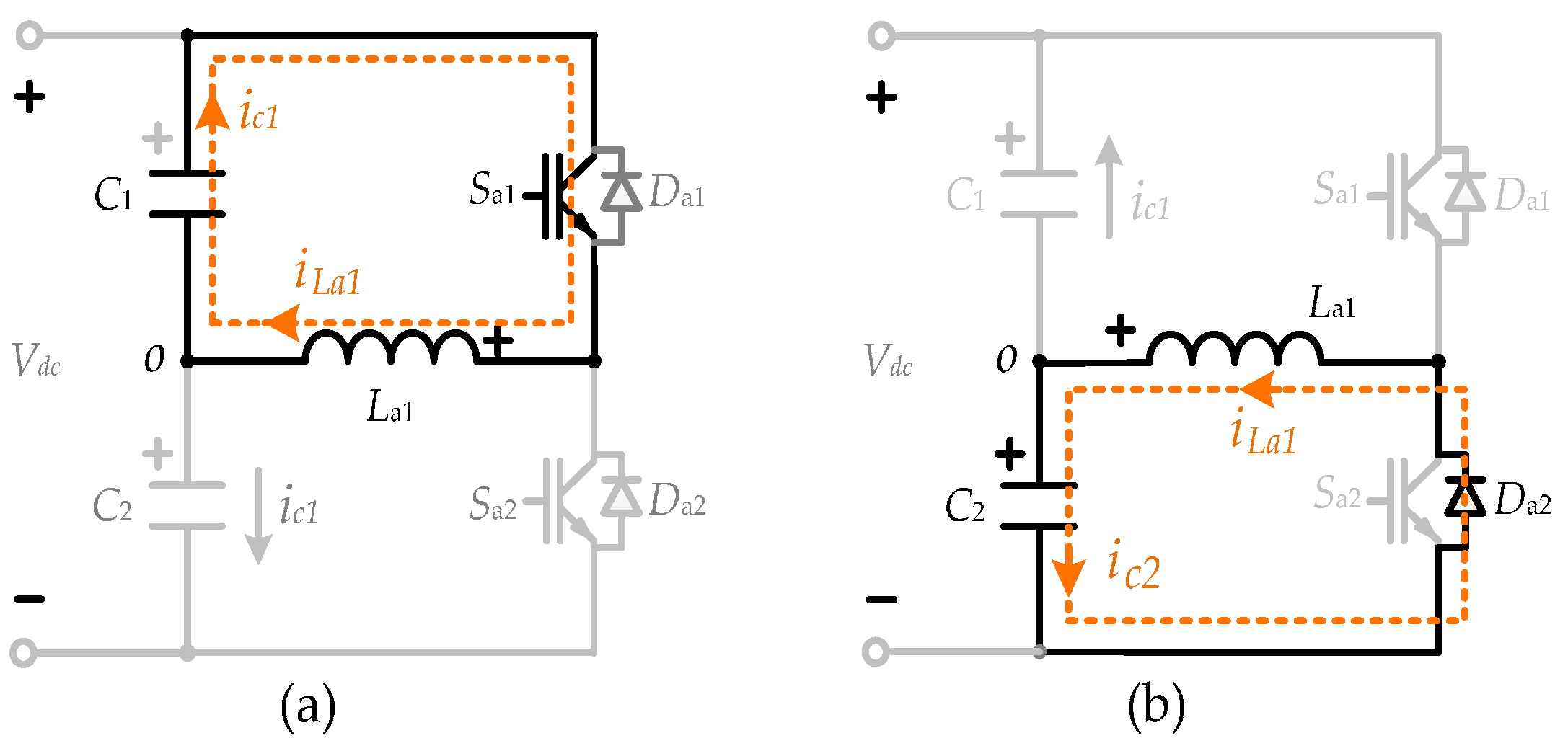
As illustrated in Figure 8, an inductor-based auxiliary circuit enables energy transmission from one capacitor to the other via the auxiliary inductor La1. Two serial switches and the serial dc-link capacitors C1, C2 are connected in series, with a resonant inductor La1 connected between their midpoints. Three steps are taken to accomplish the transfer process. For example, when vC1 > vC2, the first step is to transfer the energy stored in the upper capacitor C1 to the additional inductor La1 via Sa1 as depicted by the highlighted path in Figure 8a. The inductor current iLa1 increases while the capacitor voltage vC1 decreases during the first step. Secondly, as shown in Figure 8b, the inductor La1 is connected to the lower capacitor C2 via the anti-parallel diode Da2. The energy stored in auxiliary inductor is transferred to compensate the lack of power storage in the lower capacitor C2. During this step, the inductor current iLa1 decreases while, in contrast, the voltage of the lower capacitor vC2 increases. Once the inductor current decreases to zero, the previous conducted path will block reversely until next period. In this way, the voltage balancing between vC1 and vC2 is accomplished. The balancing process is similar when vC1 < vC2. In order to properly execute the auxiliary circuit, the adjacent two series switches in one unit cannot be turned on at the same time.
The auxiliary balancing circuits are totally independent form the main circuit. Therefore, the neutral-point voltage is settled with the characteristics of the main circuit remain uninfluenced.
5. Simulation and Experiment
To verify the performance of the proposed control strategies. The three-module single-phase 3LNPC-CR is modeled. The simulation is carried out in MATLAB/Simulink (MathWorks, Natick, MA, USA).
The capacitor voltages in one single-phase 3LNPC rectifier module is shown in Figure 9. During the first 0.3 s, the capacitor voltages are balanced using inductor-based auxiliary balancing circuit. To highlight the effect of auxiliary circuit, a resistor connected in parallel with one of the capacitors is switched on at 0.3 s. Obviously, the balance between these two capacitor voltages is broken. However, the voltages on the upper capacitor and the lower capacitor become stabilized and equalized in 0.3 s.
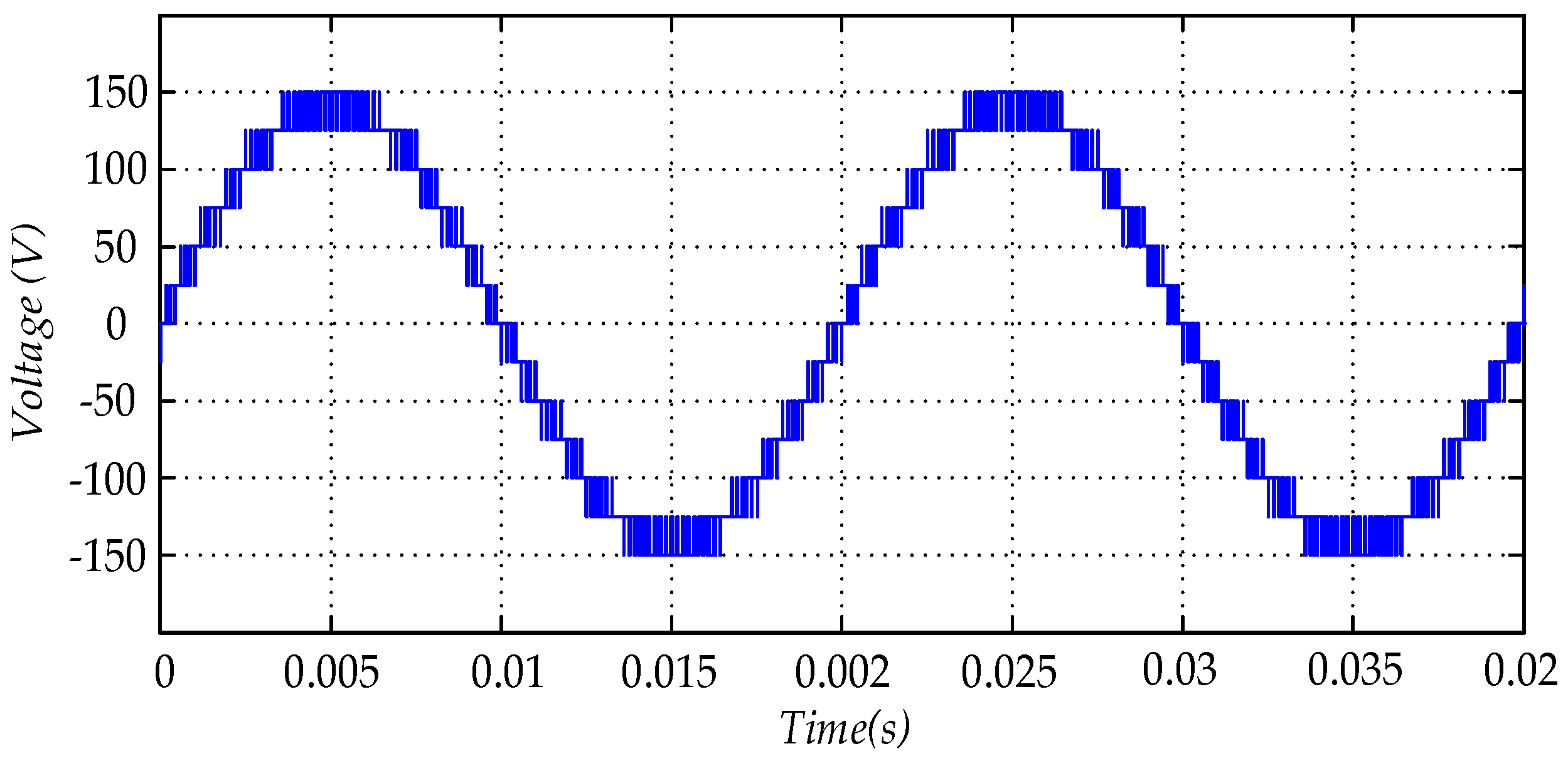
Figure 10 shows the characteristic of the input voltage of three-module single-phase 3LNPC-CR. The thirteen-level staircase voltage is generated using phase-shifted SVPWM strategy shown in Figure 4.
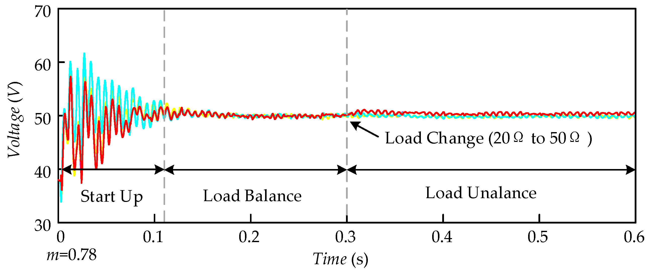
Two different cases have been simulated to verify the multi-module control strategy. During the first 0.3 s, the loads of each module are balanced. The output voltage of each module becomes constant and all of them converge to 50 V at 0.12 s. At 0.3 s, the load of module 1 is changed from 20 Ω to 50 Ω, which means the output voltages are supposed to be different without the balancing scheme. As shown in Figure 11, the voltage balancing scheme is accomplished by immediately modifying the modulation depth of each rectifier module. After little voltage fluctuation during a few switching periods, the output voltages managed to converge to 50 V. Thus, the internal-voltage balancing scheme is verified.
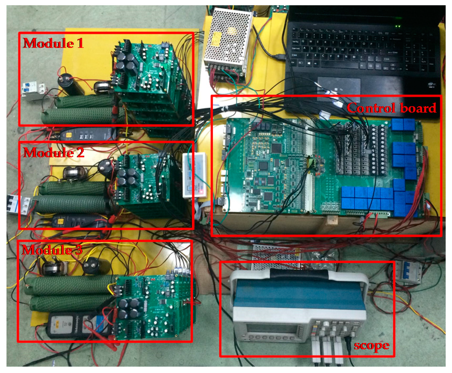
As shown in Figure 12, a three-module single phase 3LNPC-CR prototype has been built on the laboratory setup. The three-module single phase 3LNPC-CR works on the occasion of 50 Hz 75 V input voltage. When the loads are balanced, each dc-link terminal could obtain 50 V output voltage. The controller of the 3LNPC-CR is based on the EP3C55F484C8 FPGA chip. The parameters are reported in Table 3.
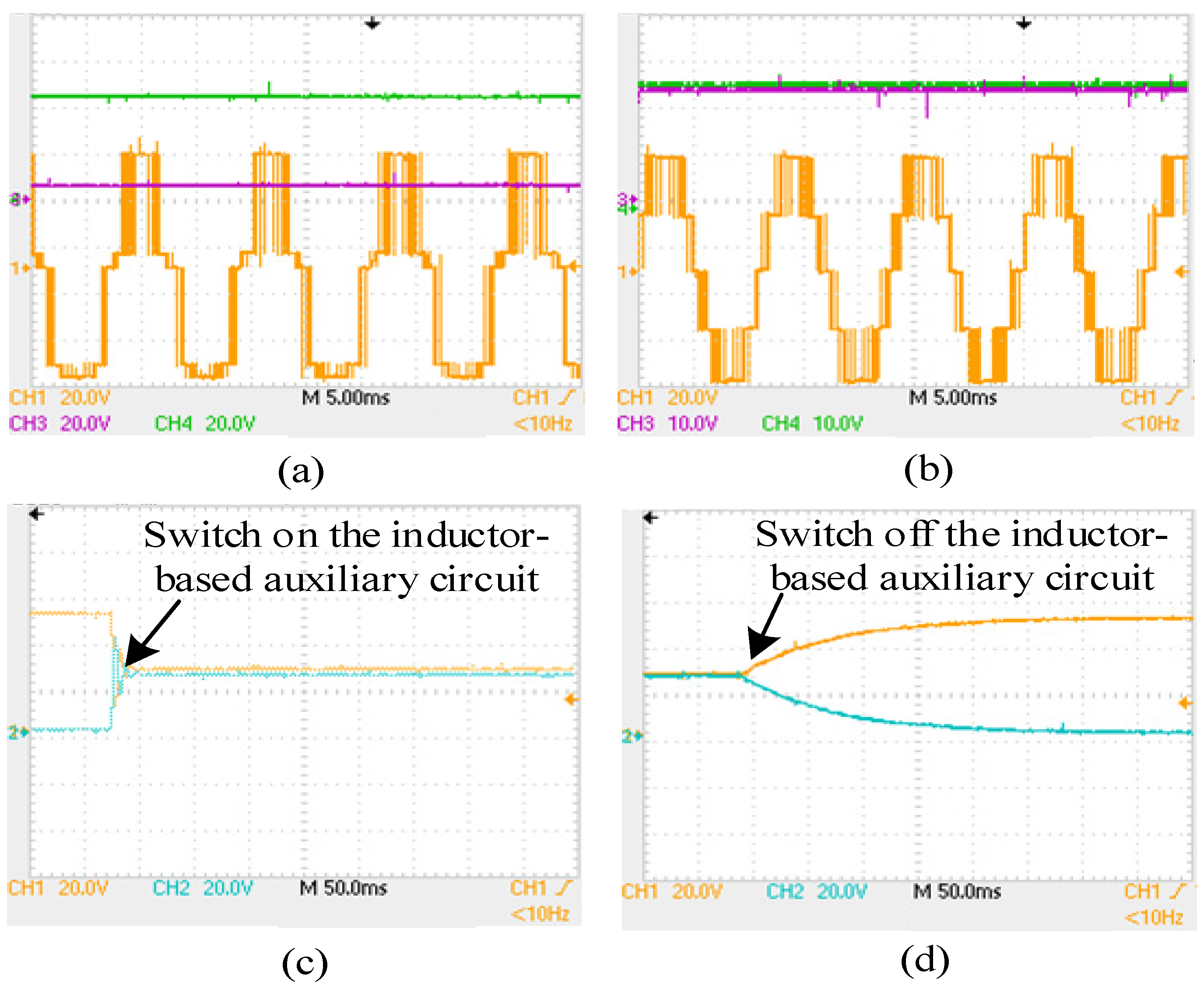
The experiment results of the internal-module voltage balancing strategy are shown in Figure 13.
Figure 13a,b shows the waveforms of dc-link voltages and ac-side input voltage in one single-phase 3LNPC rectifier module before and after the inductor-based auxiliary circuit is implemented. To assess the system dynamic performance, two types of tests have been considered. The first test switched on the inductor-based auxiliary circuit to balance the unbalanced dc-link capacitor voltage. Figure 13c shows the dynamic waveforms of dc-link capacitors when the inductor-based auxiliary balancing circuit is activated. It is obvious that the dc-link capacitor voltages converge to the reference value after several periods. In the second test, the auxiliary circuit is switched off. Figure 13d demonstrates the transient voltage of dc-link capacitors when the auxiliary balancing circuit is suddenly switched off. It is obvious that the dc-link capacitor voltages become unbalanced without the auxiliary circuit. In this way, both of these two tests verified the effectiveness of the inductor-based auxiliary circuit.
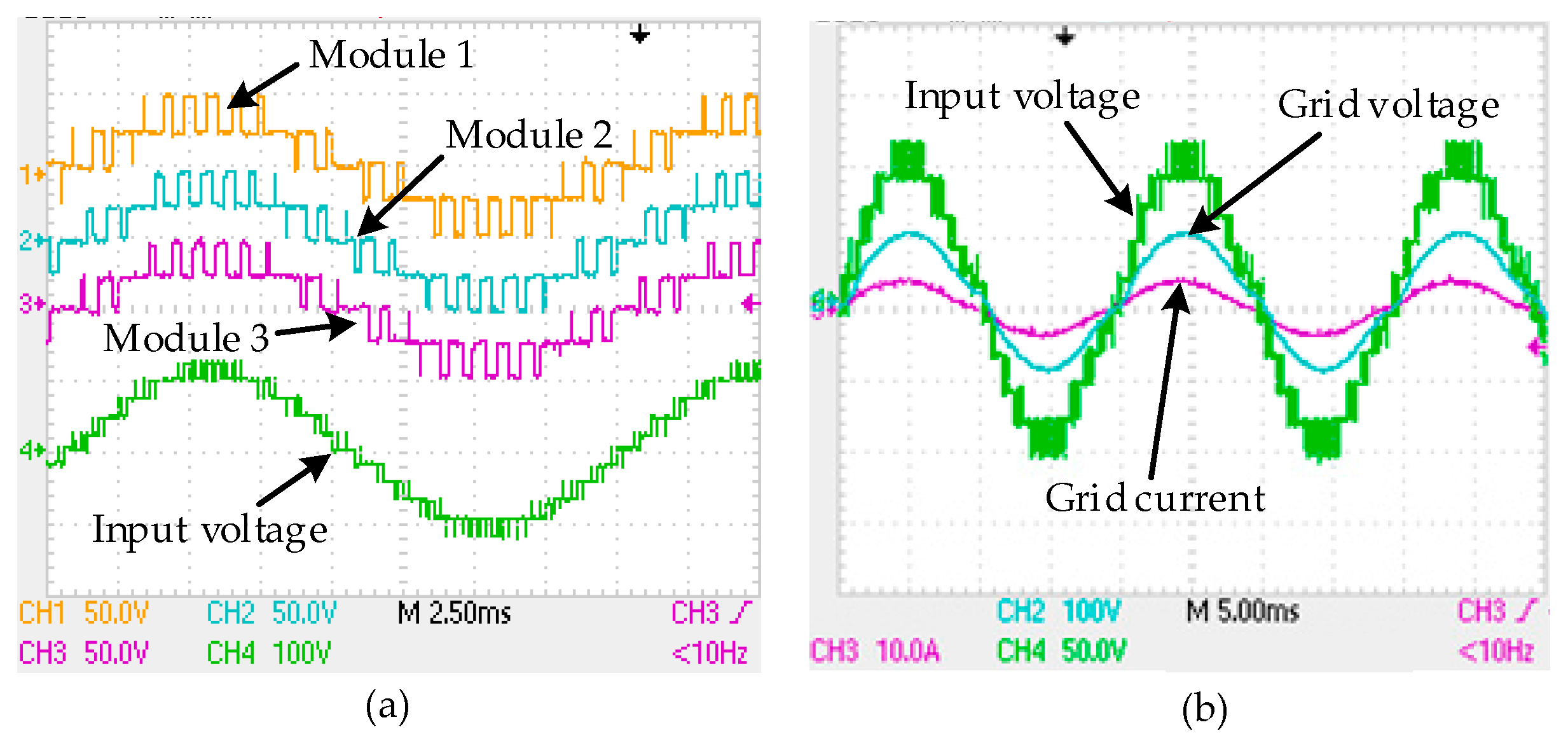
The Five-level wave form shown in Figure 14a is typical of input voltages of a 3LNPC rectifier. A Thirteen-level overall input voltage waveform is generated via the phase shift technology. It is obvious that the input voltage is identical with the simulation result. Figure 14b illustrates the grid voltage and the grid current. It is possible to notice that the grid current keeps well in phase with the grid voltage. That is to say, unity power factor is achieved. The perfect agreement between these experimental results and the former analysis is reached.
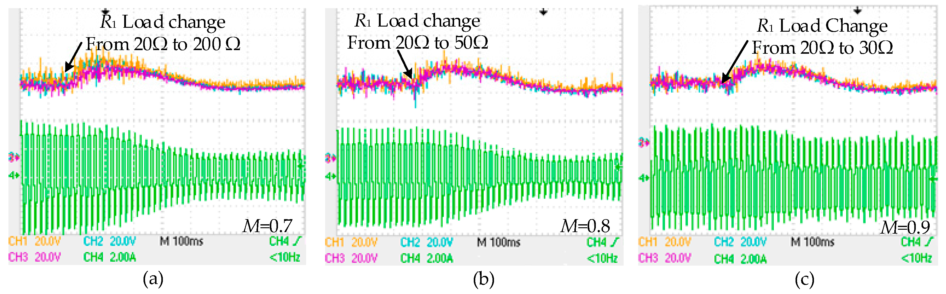
In order to verify the viability of mutual-module voltage balancing control strategy, an experiment has been carried out based on the 3LNPC-CR prototype. The resistor R1 is dynamically changed while the resistors R2 and R3 remains 20 Ω to create the unbalance of dc-loads, so that the real power transmitted to module 1 is different from module 2 and module 3. According to Formula (19), the load unbalance degree limit of a three-module 3LNPC-CR depends on its modulation index. Thus, the calculation results of the maximum load unbalance limit are verified by implementing 3LNPC-CRs with different modulation indexes.
Since the input inductance is ignored during the calculation, the balancing boundary is an approximate result. In fact, the mutual-module balancing strategy is still able to balance the dc-link voltages when the unbalance degree slightly exceeds the calculation result. However, if the unbalance degree exceeds the calculated boundary by a large margin, the balancing strategy will fail to balance the dc-link voltages. When the three-module 3LNPC-CR works in the modulation depth of 0.7, the reference voltage of each dc terminals is 47 V. According to the Formula (19), this mutual-module balancing strategy is effective when ∆ > 0.14. The maximum degree of load unbalance happens when the load resistor R1 is 200 Ω while R2 and R3 equal to 20 Ω. As shown in Figure 15a, after the load change, the dc-link voltage of module 1 increased. With the mutual-module balancing strategy, the dc-link voltages become steady and converge to 47 V. During this transition, the grid current is not changed except a reduction of the current amplitude. The balancing boundary of the three-module 3LNPC-CR with a modulation depth of 0.8 is also verified. The mutual balancing strategy functions well on the premise that ∆ > 0.5. The maximum load resistor R1 within the balancing boundary is 50 Ω, as shown in Figure 15b. The mutual-module balancing strategy is still able to balance the dc-link terminal voltages when R1 is 50 Ω while R2 and R3 equal to 20 Ω. As demonstrated in Figure 15c, with a modulation depth of 0.9, the reference value of the dc-link terminals are 41 V. The unbalance degree boundary calculated according to Formula (19) is ∆ > 0.78. The mutual-module balancing strategy managed to balance the dc-link terminal voltages when the load resistor R1 is 30 Ω. The experimental results are in accordance with the calculation results. In this way, the calculation result of the balancing boundary is verified.
6. Conclusions
Several control strategies are proposed to solve the balancing problems of single-phase 3LNPC-CR. A PI-based scheme used along with the transient current control strategy successfully obtains an expected sinusoidal grid current with unity power factor and regulated output voltages. The output voltages successfully converge to the reference value even if the loads in each module are different. The inductor-based balancing strategy is addressed to balance the dc-link voltages in a single-phase 3LNPC rectifier module. The auxiliary circuit does not have any effects on the main circuit and is controlled separately. Corresponding experiments have been carried out to verify the above features. Therefore the effectiveness of the proposed control strategy is confirmed.
Acknowledgments
This work was supported by the National Natural Science Foundations of China (Grant No. 51477144).
Author Contributions
Xu Peng and Xiaoqiong He conceived the strategy and the experiments; Pengcheng Han performed the experiments; Zeliang Shu analyzed the data; Shibin Gao contributed experiment prototype; and Xiaolan Lin wrote the paper.
Conflicts of Interest
The authors declare no conflict of interest.
References
- Kouro, S.; Malinowski, M.; Gopakumar, K.; Pou, J.; Franquelo, L.G.; Wu, B.; Rodriguez, J.; Perez, M.A.; Leon, J.I. Recent advances and industrial applications of multilevel converters. IEEE Trans. Ind. Electron. 2010, 57, 2553–2580. [Google Scholar] [CrossRef]
- Franquelo, L.G.; Leon, J.I.; Dominguez, E. Recent advances in high-power industrial applications. In Proceedings of the 2010 IEEE International Symposium on Industrial Electronics (ISIE), Bari, Italy, 4–7 July 2010; pp. 5–10. [Google Scholar]
- Vahedi, H.; Shojaei, A.A.; Chandra, A.; Al-Haddad, K. Five-level reduced-switch-count boost PFC rectifier with multicarrier PWM. IEEE Trans. Ind. Appl. 2016, 52, 4201–4207. [Google Scholar] [CrossRef]
- Vahedi, H.; Labbé, P.A.; Al-Haddad, K. Sensor-less five-level packed U-cell (PUC5) inverter operating in stand-alone and grid-connected modes. IEEE Trans. Ind. Inform. 2016, 12, 361–370. [Google Scholar] [CrossRef]
- Shu, Z.; Ding, N.; Chen, J.; Zhu, H.; He, X. Multilevel SVPWM with DC-link capacitor voltage balancing control for diode-clamped multilevel converter based STATCOM. IEEE Trans. Ind. Electron. 2013, 60, 1884–1896. [Google Scholar] [CrossRef]
- Villanueva, E.; Correa, P.; Rodriguez, J.; Pacas, M. Control of a single-phase cascaded H-bridge multilevel inverter for grid-connected photovoltaic systems. IEEE Trans. Ind. Electron. 2009, 56, 4399–4406. [Google Scholar] [CrossRef]
- Cecati, C.; Dell’Aquila, A.; Liserre, M.; Monopoli, V.G. Design of H-bridge multilevel active rectifier for traction systems. IEEE Trans. Ind. Appl. 2003, 39, 1541–1550. [Google Scholar] [CrossRef]
- Tao, X.; Li, Y.; Sun, M. A Pi-based control scheme for primary cascaded H-bridge rectifier in transformerless traction converters. In Proceedings of the International Conference on Electrical Machines and Systems, Incheon, Korea, 10–13 October 2010; pp. 824–828. [Google Scholar]
- Chuanhong, Z.; Dujic, D.; Mester, A.; Steinke, J.K.; Weiss, M.; Lewdeni-Schmid, S.; Chaudhuri, T.; Stefanutti, P. Power electronic traction transformer—Medium voltage prototype. IEEE Trans. Ind. Electron. 2014, 61, 3257–3268. [Google Scholar]
- Malinowski, M.; Gopakumar, K.; Rodriguez, J.; Perez, M.A. A survey on cascaded multilevel inverters. IEEE Trans. Ind. Electron. 2010, 57, 2197–2206. [Google Scholar] [CrossRef]
- Vahedi, H.; Al-Haddad, K. A novel multilevel multioutput bidirectional active buck PFC rectifier. IEEE Trans. Ind. Electron. 2016, 63, 5442–5450. [Google Scholar] [CrossRef]
- Sebaaly, F.; Vahedi, H.; Kanaan, H.Y.; Moubayed, N.; Al-Haddad, K. Design and implementation of space vector modulation-based sliding mode control for grid-connected 3L-NPC inverter. IEEE Trans. Ind. Electron. 2016, 63, 7854–7863. [Google Scholar] [CrossRef]
- Rodriguez, J.; Bernet, S.; Steimer, P.K.; Lizama, I.E. A survey on neutral-point-clamped inverters. IEEE Trans. Ind. Electron. 2010, 57, 2219–2230. [Google Scholar] [CrossRef]
- Marzoughi, A.; Imaneini, H. Optimal selective harmonic elimination for cascaded H-bridge-based multilevel rectifiers. IET Power Electron. 2014, 7, 350–356. [Google Scholar] [CrossRef]
- Dell’Aquila, A.; Liserre, M.; Monopoli, V.G.; Rotondo, P. Overview of PI-based solutions for the control of DC buses of a single-phase H-bridge multilevel active rectifier. IEEE Trans. Ind. Appl. 2008, 44, 857–866. [Google Scholar] [CrossRef]
- Shu, Z.; Kuang, Z.; Wang, S.; Peng, X.; He, X. Diode-clamped three-level multi-module cascaded converter based power electronic traction transformer. In Proceedings of the IEEE 2nd International Future Energy Electronics Conference (IFEEC), Taipei, Taiwan, 1–4 November 2015. [Google Scholar]
- Vahedi, H.; Labbe, P.A.; Al-Haddad, K. Balancing three-level neutral point clamped inverter DC bus using closed-loop space vector modulation: Real-time implementation and investigation. IET Power Electron. 2016, 9, 2076–2084. [Google Scholar] [CrossRef]
- Celanovic, N.; Boroyevich, D. A comprehensive study of neutral-point voltage balancing problem in three-level neutral-point-clamped voltage source PWM inverters. IEEE Trans. Power Electron. 2000, 15, 242–249. [Google Scholar] [CrossRef]
- Shu, Z.; He, X.; Wang, Z.; Qiu, D.; Jing, Y. Voltage balancing approaches for diode-clamped multilevel converters using auxiliary capacitor-based circuits. IEEE Trans. Power Electron. 2013, 28, 2111–2124. [Google Scholar] [CrossRef]
- Shu, Z.; Zhu, H.; He, X.; Ding, N.; Yang, Y. One-inductor-based auxiliary circuit for DC-link capacitor voltage equalisation of diode-clamped multilevel converter. IET Power Electron. 2013, 6, 1339–1349. [Google Scholar]
- Peng, X.; He, X.; Han, P.; Guo, A.; Shu, Z.; Gao, S. Smooth switching technique for voltage balance management based on three-level neutral point clamped cascaded rectifier. Energies 2016, 9, 803. [Google Scholar] [CrossRef]
- Moeini, A.; Iman-Eini, H.; Marzoughi, A. DC link voltage balancing approach for cascaded H-bridge active rectifier based on selective harmonic elimination-pulse width modulation. IET Power Electron. 2015, 8, 583–590. [Google Scholar] [CrossRef]
- Cecati, C.; Dell’Aquila, A.; Liserre, M.; Monopoli, V.G. A passivitybased multilevel active rectifier with adaptive compensation for traction applications. IEEE Trans. Ind. Appl. 2003, 39, 1404–1413. [Google Scholar] [CrossRef]
- Dell’Aquila, A.; Liserre, M.; Monopoli, V.G.; Rotondo, P. An energy-based control for an n-H-bridges multilevel active rectifier. IEEE Trans. Ind. Electron. 2005, 52, 670–678. [Google Scholar] [CrossRef]
- Zhao, T.; Wang, G.; Bhattacharya, S.; Huang, A.Q. Voltage and power balance control for a cascaded H-bridge converter-based solid-state transformer. IEEE Trans. Power Electron. 2013, 28, 1523–1532. [Google Scholar] [CrossRef]
Figure 1.
Circuit configuration of Single phase 3LNPC-CR.

Figure 2.
Voltage vectors for a single phase 3LNPC rectifier.

Figure 3.
Voltage vectors diagram for a single phase 3LNPC rectifier.

Figure 4.
Phase-shifted carrier-based SVPWM technique.

Figure 5.
Control scheme for grid current and overall voltage.
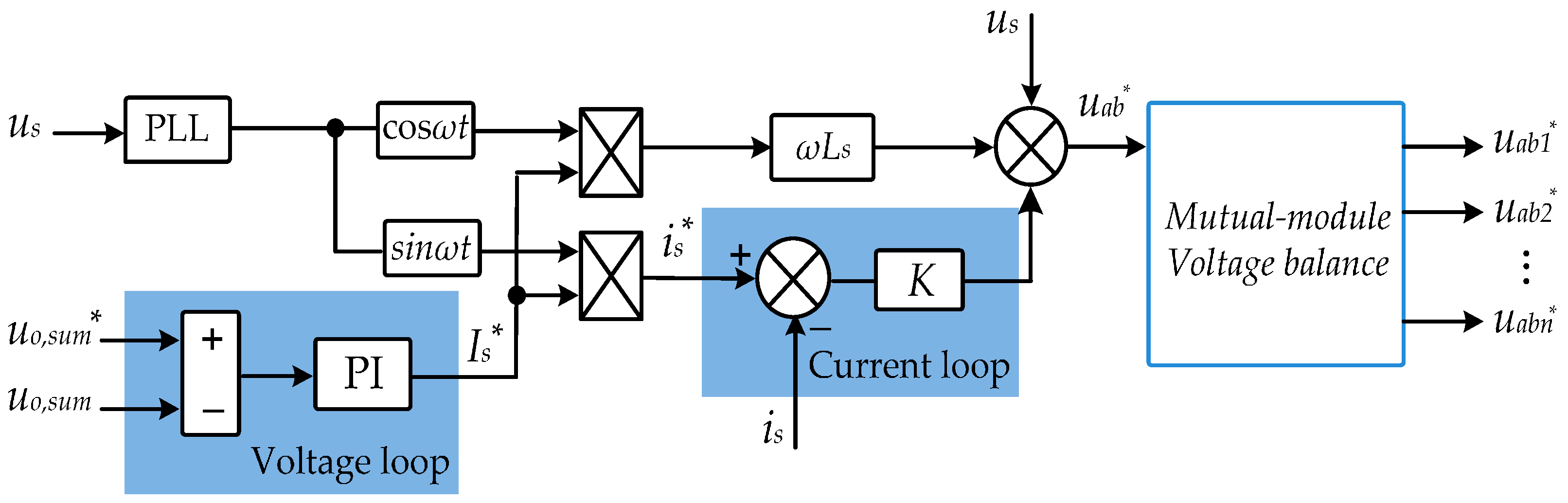
Figure 6.
Mutual-module voltage balancing scheme.
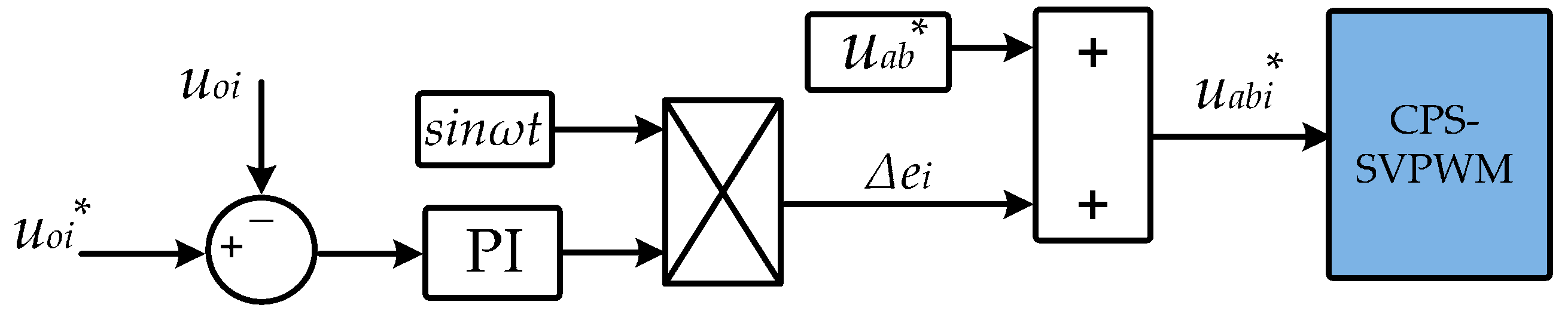
Figure 7.
Capacitor-based voltage balancing scheme: (a) C1 charges Ca1; and (b) Ca1 charges C2.
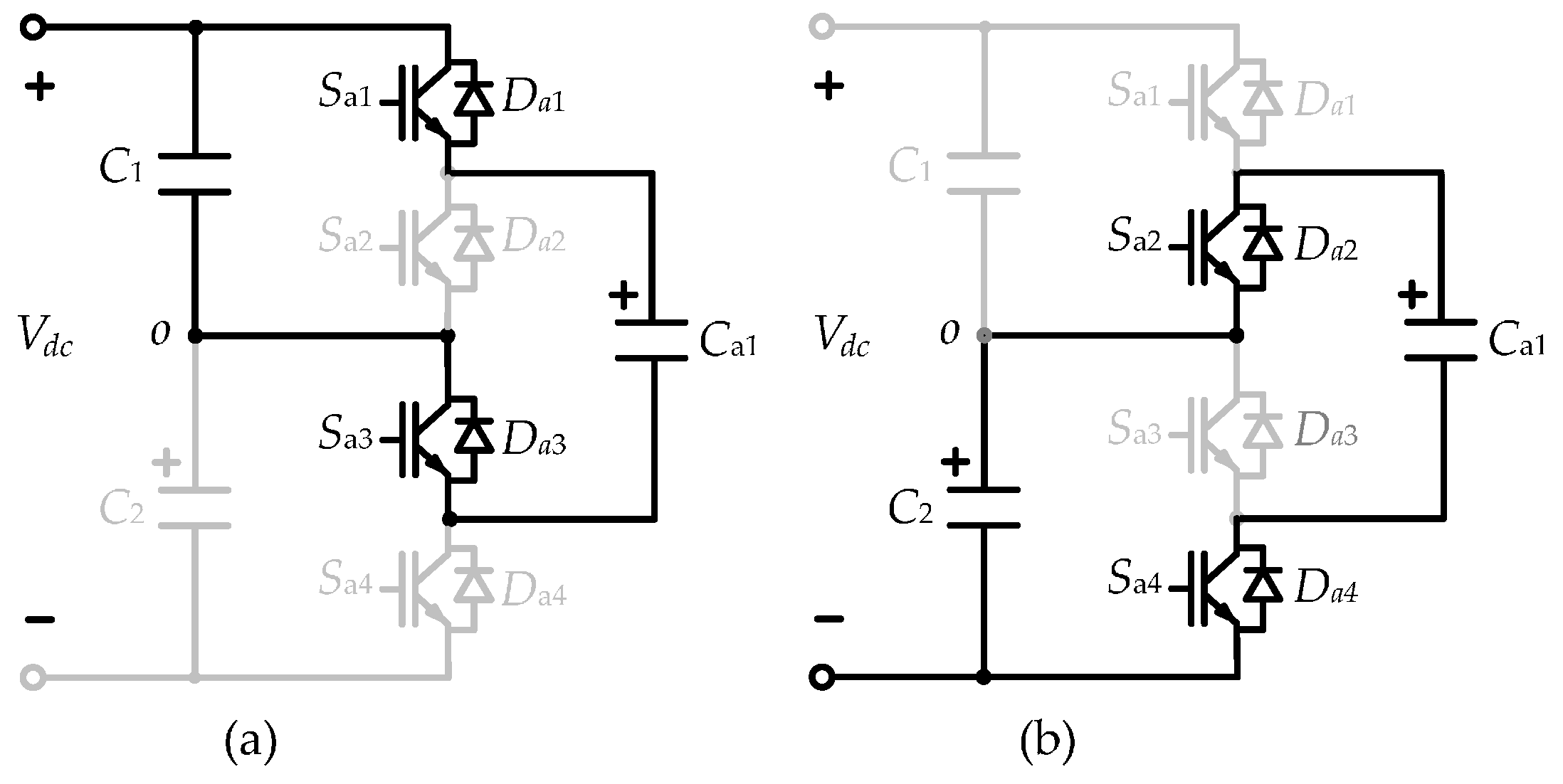
Figure 8.
Inductor-based voltage balancing scheme when vC1 > vC2: (a) C1 charges La1; and (b) La1 charges C2.
Figure 8.
Inductor-based voltage balancing scheme when vC1 > vC2: (a) C1 charges La1; and (b) La1 charges C2.

Figure 9.
Capacitor voltages with inductor-based auxiliary balancing circuit.

Figure 10.
Input voltage of three-module 3LNPC-CR.

Figure 11.
Output voltages using multi-module balancing scheme.

Figure 12.
Prototype of three-module single phase 3LNPC-CR.

Figure 13.
Experiment results: (a) dc-link capacitor voltages and input voltage of 3LNPC rectifier without auxiliary circuit (CH1: the input voltage of 3LNPC rectifier, CH3: the dc-link voltage on capacitor C1, CH4: the dc-link voltage on capacitor C2); (b) dc-link capacitor voltages and input voltage when auxiliary circuit is implemented (CH1: the input voltage of 3LNPC rectifier, CH3: the dc-link voltage on capacitor C1, CH4: the dc-link voltage on capacitor C2); (c) dynamic waveform of dc-link capacitor voltages (CH1: the dc-link voltage on capacitor C1, CH2: the dc-link voltage on capacitor C2); and (d) dynamic waveform of dc-link capacitor voltages (CH1: the dc-link voltage on capacitor C1, CH2: the dc-link voltage on capacitor C2).

Figure 14.
Experiment results: (a) Input voltages of the 3LNPC rectifier and three-module 3LNPC-CR (CH1: the input voltage of module 1, CH2: the input voltage of module 2, CH3: the input voltage of module 3, CH4: the input voltage of the three-module 3LNPC-CR); and (b) AC-side voltage and current of the three-module 3LNPC-CR (CH2: the grid voltage of the three-module 3LNPC-CR, CH3: the grid current of the three-module 3LNPC-CR, CH4: the input voltage of the three-module 3LNPC-CR).

Figure 15.
Experiment results: (a) M = 0.7, R1 changes from 20 Ω to 200 Ω (CH1: dc-link voltage of module 1, CH2: dc-link voltage of module2, CH3: dc-link voltage of module3, CH4: grid current of the three-module 3LNPC-CR); (b) M = 0.8, R1 changes from 20 Ω to 50 Ω (CH1: dc-link voltage of module 1, CH2: dc-link voltage of module2, CH3: dc-link voltage of module 3, CH4: grid current of the three-module 3LNPC-CR); and (c) M = 0.9, R1 changes from 20 Ω to 30 Ω (CH1: dc-link voltage of module 1, CH2: dc-link voltage of module 2, CH3: dc-link voltage of module 3, CH4: grid current of the three-module 3LNPC-CR).


Table 1.
Switching states when Is > 0.
| Vectors | Sa | Sb | uab | C1 | C2 | Categories |
|---|---|---|---|---|---|---|
| V1 | p | p | 0 | no effect | no effect | Z |
| V2 | p | o | VC1 | Charge | no effect | SP |
| V3 | o | n | VC2 | no effect | charge | SP |
| V4 | p | n | VC1 + VC2 | charge | charge | LP |
| V5 | o | o | 0 | no effect | no effect | Z |
| V6 | n | o | −VC2 | no effect | discharge | SN |
| V7 | o | p | −VC1 | discharge | no effect | SN |
| V8 | n | p | −VC1 − VC2 | discharge | discharge | LN |
| V9 | n | n | 0 | no effect | no effect | Z |
Table 2.
The principle of internal-module voltage balancing.
| VC1 > VC2, is > 0 | VC1 > VC2, is < 0 | VC1 < VC2, is < 0 | VC1 < VC2, is > 0 |
|---|---|---|---|
| SP = V3 | SP = V2 | SP = V3 | SP = V2 |
| SN = V7 | SN = V6 | SN = V7 | SN = V6 |
Table 3.
Parameters of experiment.
| Parameter Name | Parameter Value |
|---|---|
| Number of modules | 3 |
| Voltage source | 75 V/50 Hz |
| dc-link capacitor | 2200 µF |
| Inductance of auxiliary circuit | 1 mH |
| Inductance of LC filter | 1 mH |
| Capacitance of LC filter | 2200 µF |
| Switching frequency | 2 kHz |
© 2017 by the authors. Licensee MDPI, Basel, Switzerland. This article is an open access article distributed under the terms and conditions of the Creative Commons Attribution (CC BY) license (http://creativecommons.org/licenses/by/4.0/).
Share and Cite
MDPI and ACS Style
He, X.; Lin, X.; Peng, X.; Han, P.; Shu, Z.; Gao, S. Control Strategy of Single-Phase Three Level Neutral Point Clamped Cascaded Rectifier. Energies 2017, 10, 592. https://doi.org/10.3390/en10050592
AMA Style
He X, Lin X, Peng X, Han P, Shu Z, Gao S. Control Strategy of Single-Phase Three Level Neutral Point Clamped Cascaded Rectifier. Energies. 2017; 10(5):592. https://doi.org/10.3390/en10050592
Chicago/Turabian StyleHe, Xiaoqiong, Xiaolan Lin, Xu Peng, Pengcheng Han, Zeliang Shu, and Shibin Gao. 2017. "Control Strategy of Single-Phase Three Level Neutral Point Clamped Cascaded Rectifier" Energies 10, no. 5: 592. https://doi.org/10.3390/en10050592
Note that from the first issue of 2016, this journal uses article numbers instead of page numbers. See further details here.