
A Switching Frequency Optimized Space Vector Pulse Width Modulation (SVPWM) Scheme for Cascaded Multilevel Inverters

1
School of Automation, Guangdong University of Technology, Guangzhou 510006, China
2
School of Electrical and Information Engineering, Changsha University of Science and Technology, Changsha 410004, China
*
Author to whom correspondence should be addressed.
Energies 2017, 10(5), 725; https://doi.org/10.3390/en10050725
Submission received: 21 March 2017
/
Revised: 3 May 2017
/
Accepted: 12 May 2017
/
Published: 21 May 2017
(This article belongs to the Section I: Energy Fundamentals and Conversion)
Abstract
:This paper presents a novel switching frequency optimized space vector pulse width modulation (SVPWM) scheme for cascaded multilevel inverters. The proposed SVPWM is developed in a α′β′ coordinate system, in which the voltage vectors have only integer entries and the absolute increment of coordinate values between adjacent vectors is equal to dc-bus voltage of power cells (1 pu). The new SVPWM scheme is built with three categories of switching paths. During each switching path, the change of one phase voltage is limited in 1 pu. This contributes to decrease the number of commutations of switches. The proposed SVPWM scheme is validated on a 7-level cascaded inverter and the results show that it significantly outperforms traditional SVPWM schemes in terms of decreasing the number of switch commutations.
1. Introduction
Multilevel inverters have been selected as a preferred power converter topology for high voltage and high power applications [1,2]. They are widely used in medium voltage motor driver [3], high-voltage direct current (HVDC) transmission systems [4], static var generator (SVG) [5], active power filter (APF) [6] and other applications [7,8]. Several topologies for multilevel inverters have been proposed in the past decades, including diode-clamped [9], flying capacitor [1], cascaded H-bridge [10] and modular multilevel [11]. For a given multilevel converter topology, modulation scheme is a key factor [12,13,14,15,16,17]. Among various modulation schemes, space vector pulse width modulation (SVPWM) scheme is an attractive candidate due to its flexibility to optimize switching waveforms and its convenience to be implemented in digital signal processors [1,12,13,14]. Generally, most SVPWM schemes can be implemented with the following three steps:
- (1)
- Locate the reference voltage vector and select three nearest space vectors.
- (2)
- Calculate the duty cycles for the three space vectors.
- (3)
- Generate the switching sequences with specific constraint.
Because the space vector diagram of multilevel inverters is comprised of equilateral triangles in traditional αβ coordinate system, the location of reference voltage vector and the duty cycles of the three nearest vectors are obtained with extensive computation. Consequently, the implementation of SVPWM schemes in αβ coordinate system usually becomes more complex as the number of levels increases. To speed up Step 1 and Step 2, various coordinate systems have been developed [18,19,20,21].
The determination of redundancies with specific constraint in Step 3 remains a big challenge for SVPWM schemes. In order to decrease the number of commutations of switches, some switching techniques have been developed in [22,23]. By carefully selecting redundant switching positions in upper type triangle, lower type triangle and the section number, a minimum loss SVPWM scheme was proposed in [22]. However, as the number of level increases, the selecting complexity of the redundancies increases and no generalized technique for redundancies and switching state transitions is developed. Based on two mappings, a SVPWM scheme is proposed in [23]. Because the different “modes” need to be determined and the region number of the modulation triangle should be calculated in the SVPWM scheme, the rule of determining the switching sequences is still challenging so far.
In this paper, a novel switching frequency optimized SVPWM scheme is proposed and the main contributions are summarized below: (1) the proposed SVPWM scheme is developed in a α′β′ coordinate system; (2) The change of one phase voltage is limited in 1 pu during each switching path; (3) The experimental results show that the proposed method significantly outperforms the traditional SVPWM schemes in terms of decreasing the number of commutations of switches.
The paper is organized as follows: Section 2 describes the concepts of basic switching mode and switching path. Section 3 presents the principle of the SVPWM scheme. The experimental results and comparative analysis are presented to validate the theoretical analysis in Section 4. Finally, the conclusions are presented in Section 5.
2. Basic Switching Modes and Switching Paths
2.1. α′β′ Coordinate System
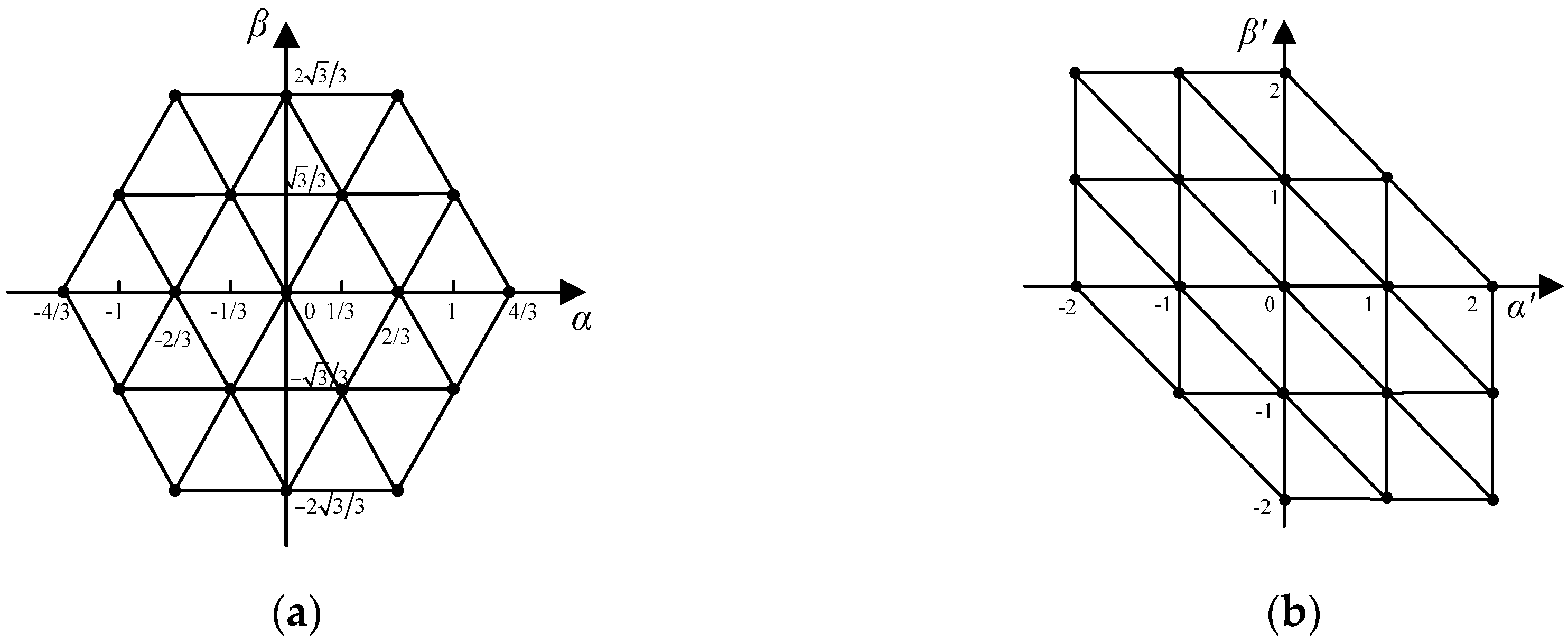
A α′β′ coordinate system is our developed coordinate system in [24]. In the α′β′ coordinate system, voltage vectors have integer entries and the absolute coordinate increment between adjacent vectors is equal to 1. The transformation matrix among the α′β′ coordinate system, the traditional αβ coordinate system [1] and abc coordinate system are written in Equation (1):
where, a, b and c are the normalized three phase voltages of multilevel inverters. [α β]T and [α′ β′]T are the coordinate values of [a b c]T in the traditional αβ coordinate system and the α′β′ coordinate system, respectively.
The projections of vectors for 3-level inverter in the αβ and α′β′ coordinate system are shown in Figure 1, where, each vector is represented by one dot.
2.2. Three Basic Switching Modes
The basic switching mode and switching path are defined as follows:
(1) Basic switching mode: the value of a, b or c is changed with 1 pu between two adjacent switching states. There are three kinds of basic switching modes in space vector diagram, and the three kinds of basic switching modes is named as diagonal switching mode, vertical switching mode, and horizontal switching mode in the paper, respectively. The three kinds of basic switching modes are illustrated in Figure 2.
(2) Switching path: a trajectory is formed by a finite number of basic switching modes in turn.
The increment expression of Equation (1) is described in Equation (2).
where, Δa, Δb and Δc are the increment of a, b and c in the abc coordinate system. Δα′ and Δβ′ are the increment of α′ and β′.
If phase A voltage is changed with 1 pu in one basic switching mode, subject to:
Substituting Equation (3) in Equation (2), the expression of the diagonal switching mode is written in Equation (4):
If phase B voltage is changed with 1 pu in one basic switching mode, subject to:
Substituting Equation (5) in Equation (2), the expression of the vertical switching mode is written in Equation (6):
If phase C voltage is changed with 1 pu in one basic switching mode, subject to:
Substituting Equation (7) in Equation (2), the expression of the horizontal switching mode is written in Equation (8):
2.3. Characteristics of Switching Paths
It is shown in Figure 1b and Figure 2 that any triangle is formed by the above-mentioned three basic switching modes. If a switching path is composed of three sides of a triangle by end to end, the constraint relationships of the realization of the starting vector before and after the switching path can be written-in Equation (9):
where, and are the realization of the starting vector before and after switching path, respectively. The sign of (1, 1, 1) is determined by the direction of switching path. If the direction of switching path is clockwise, the sign is positive, otherwise the sign is negative.
However, if the switching path is composed of four sides of a quadrangle by end to end, the constraint relationships of the realization of the starting vectors before and after switching path can be written as:
There are three kinds of quadrangles formed by right triangle △A and △B, and the three kinds of quadrangles are shown in Figure 3.
As described above, if switching paths consist of the four sides of the quadrangles, the proposed SVPWM scheme will be achieved.
3. The Proposed SVPWM Scheme
3.1. Trajectory and Traversing Graphs of Reference Voltage Vector
Generally, the three normalized phase voltages ar, br and cr for reference voltage vector Vr can be defined in Equation (11):
where, Vm and ω are the peak voltage and angular frequency. E is dc-bus voltage of power cells.
Substituting Equation (11) in Equation (1):
where, is the coordinate values of Vr.
Equation (12) can be rewritten as:
Figure 5 demonstrates the different traversing graphs of reference voltage vector for 7-level inverter with different modulation indexes.
Where, m is modulation index, and the red and green ellipses are the trajectories of reference voltage vector with maximum modulation index and minimum modulation index in the corresponding case. If m is between maximum and minimum modulation index, the trajectories of reference voltage vector is plotted with cyan ellipse. As shown in Figure 5, any traversing graph is composed of three kinds of quadrilaterals.
3.2. Switching Path Planning
As shown in Figure 3, there are two common vertexes, named as interface vector ① and interface vector ②. If the interface vector is chosen as a starting vector, the three vectors in the same triangle can be applied with two basic switching modes. Otherwise, at least three basic switching modes are needed.
For example, if interface vector ① (V10) is chosen as the starting vector in △A in Figure 3a, the three vectors can be applied with the switching path V10→V11→V12.If interface vector ② (V12) is chosen as starting vector, the three vectors can be applied with the switching path V12→V11→V10. However, if vector V11 is chosen as a starting vector, the three vectors is applied with the switching path V11→V12→V11→V10 or V11→V10→V11→V12. Hence, the non-common vertexes should be not chosen as a starting vector in the proposed SVPWM scheme.
The switching paths of the proposed SVPWM scheme are divided into three categories: switching paths in a triangle, switching paths not in a triangle but in a quadrilateral and switching paths between quadrilaterals.
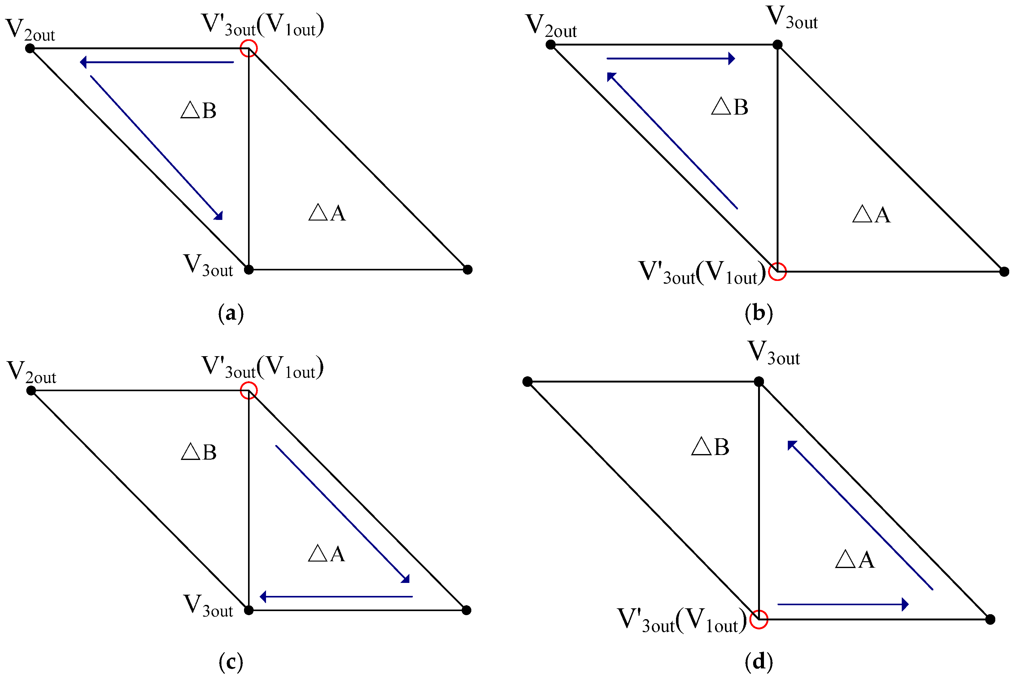
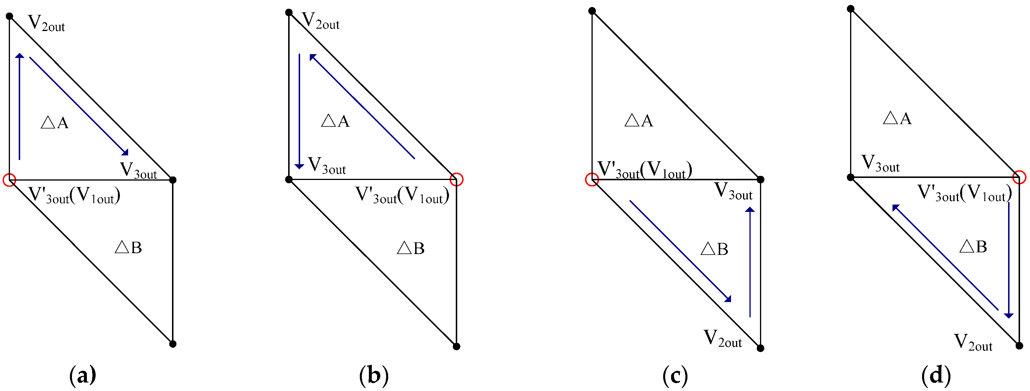
3.2.1. Switching Paths in a Triangle
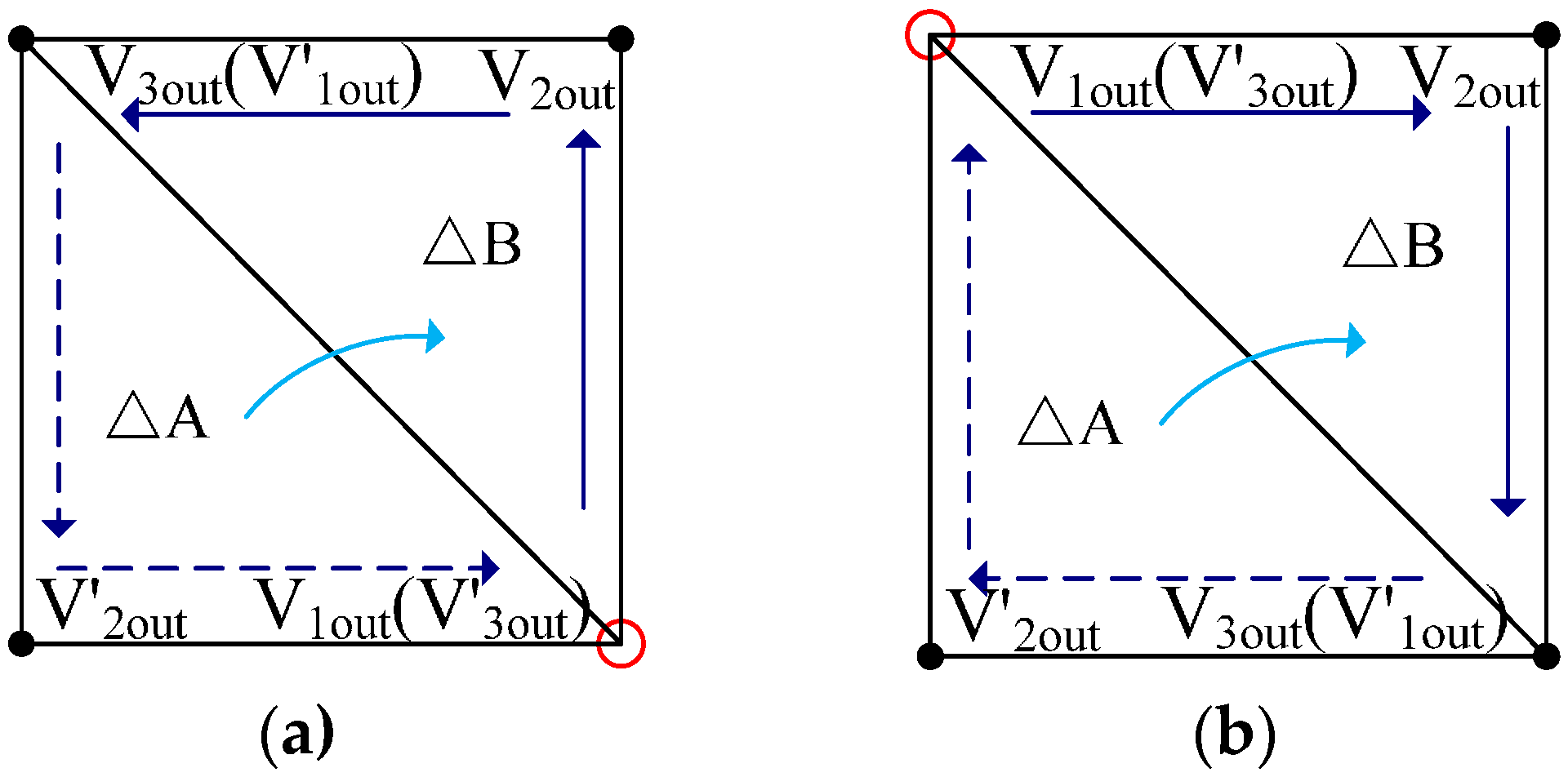
The switching paths in the same triangle for the three kinds of quadrangles are illustrated in Figure 6, Figure 7 and Figure 8, respectively, where, V′xout(x = 1, 2, 3) are the first, the second and the third vector in the previous switching path, and Vxout(x = 1, 2, 3) are the first, the second and the third vector in the current switching path. The vertex with red circles is the third vector in the previous switching path. The direction of the switching path is marked with blue arrows.
3.2.2. Switching Paths not In a Triangle but in a Quadrilateral
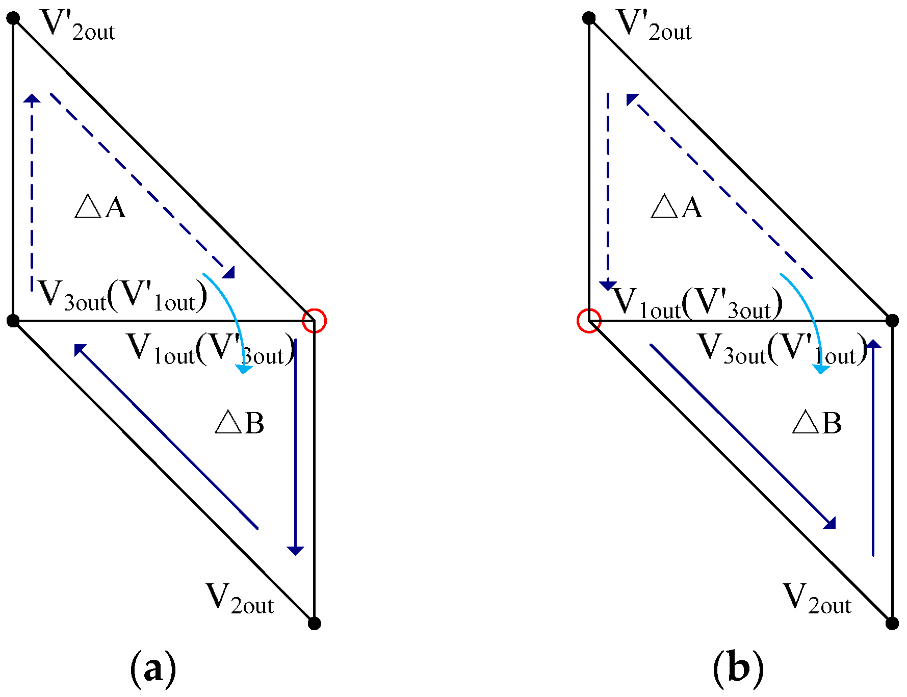
The feature in this situation is that the switching path is from △A into △B. The switching paths for the three kinds of quadrangles are shown in Figure 9, Figure 10 and Figure 11, respectively. Where, the solid and dashed arrows represent the direction of the current switching path and the previous switching path, respectively. The cyan arrows are the locus of reference vector.
3.2.3. Switching Paths between Quadrilaterals
The feature in this situation is that the switching path is from △B into △A. The transition graph between the first kind of quadrilateral and other kinds of quadrilaterals, the transition graph between the second kind of quadrilateral and other kinds of quadrilaterals, and the transition graph between the third kind of quadrilateral and other kinds of quadrilaterals are shown in Figure 12a–c, respectively. In Figure 12, AX (X = 1, 2, 3) and BX (X = 1, 2, 3) represent △A and △B triangle in the Xth kind of quadrilateral, and AX (AY) (X ≠ Y) represents the common △A triangle in Xth and Yth kind of quadrilateral. V4x (x = 1, 2, …, 9, 10), V5x (x = 1, 2, …, 9, 10) and V6x (x = 1, 2, …, 9, 10) are the vectors in the transition graph. The feasible switching paths between different kinds of quadrilaterals are listed in Table 2, Table 3 and Table 4.
3.3. Realization of Vectors
Some vectors have redundant switching states when transformed back to abc coordinate system. The realizations of vectors in the SVPWM scheme are classified in two categories: the realization of the first vector and the realization of other vectors.
3.3.1. Realization of the First Vector
Realization of the first vector is obtained with the following steps:
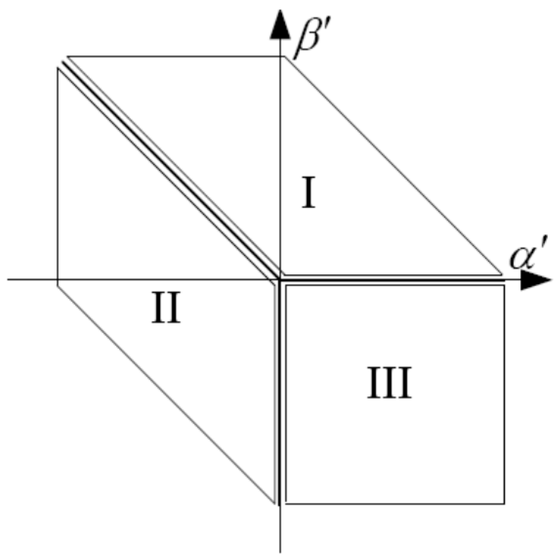
Step (1): Divide the space vector diagram into 3 zones, as shown in Figure 13.
Step (2): Identify the number of zone for the first vector.
Step (3): If the first vector was located in zone I, the realization of the first vector is obtained with the realization (−n, n, n) of vector (−2n, 2n), and the switching path consists of the first kind of quadrilaterals.
Step (4): If the first vector was located in zone II, the realization of the first vector is obtained with the realization (−n, n, n) of vector (−2n, 2n), and the switching path consists of the second kind of quadrilaterals.
Step (5): If the first vector was located in zone III, the realization of the first vector is obtained with the realization (n, n, −n) of vector (2n, 0), and the switching path is comprised of the third kind of quadrilaterals.
For simplicity, the realization of vector (2, −1) for 5-level inverter is illustrated in Figure 14. Here, vector(2, −1) is located in Zone III, and the realization of vector (4, 0) is (2, 2, −2).The switching path (4, 0)→(3, 0) →(3, −1)→(2, −1) is chosen in the α′β′ coordinate system, and the corresponding switching path (2, 2, −2)→(2, 2, −1)→(2, 1, −1)→(2, 1, 0) is obtained in abc coordinate system. Hence, the realization of vector (4, 0) is (2, 1, 0).
3.3.2. Realization of Other Vectors
Upon the realization of the first vector, the realization of other vectors can be achieved with the increment relationships between (a, b, c) and (α′, β′) in the three basic switching modes, as shown in Figure 15.
3.4. Flowchart of the Implementation of the SVPWM Scheme
The flowchart of the implementation of the SVPWM scheme is shown in Figure 16. The location of reference voltage vector and the selection strategy for the nearest three vectors can be obtained in [24]. The planning of the switching paths is demonstrated in Section 3.2, and the realization of vectors is described in Section 3.3.
4. Experimental Results
4.1. Experimental Setup
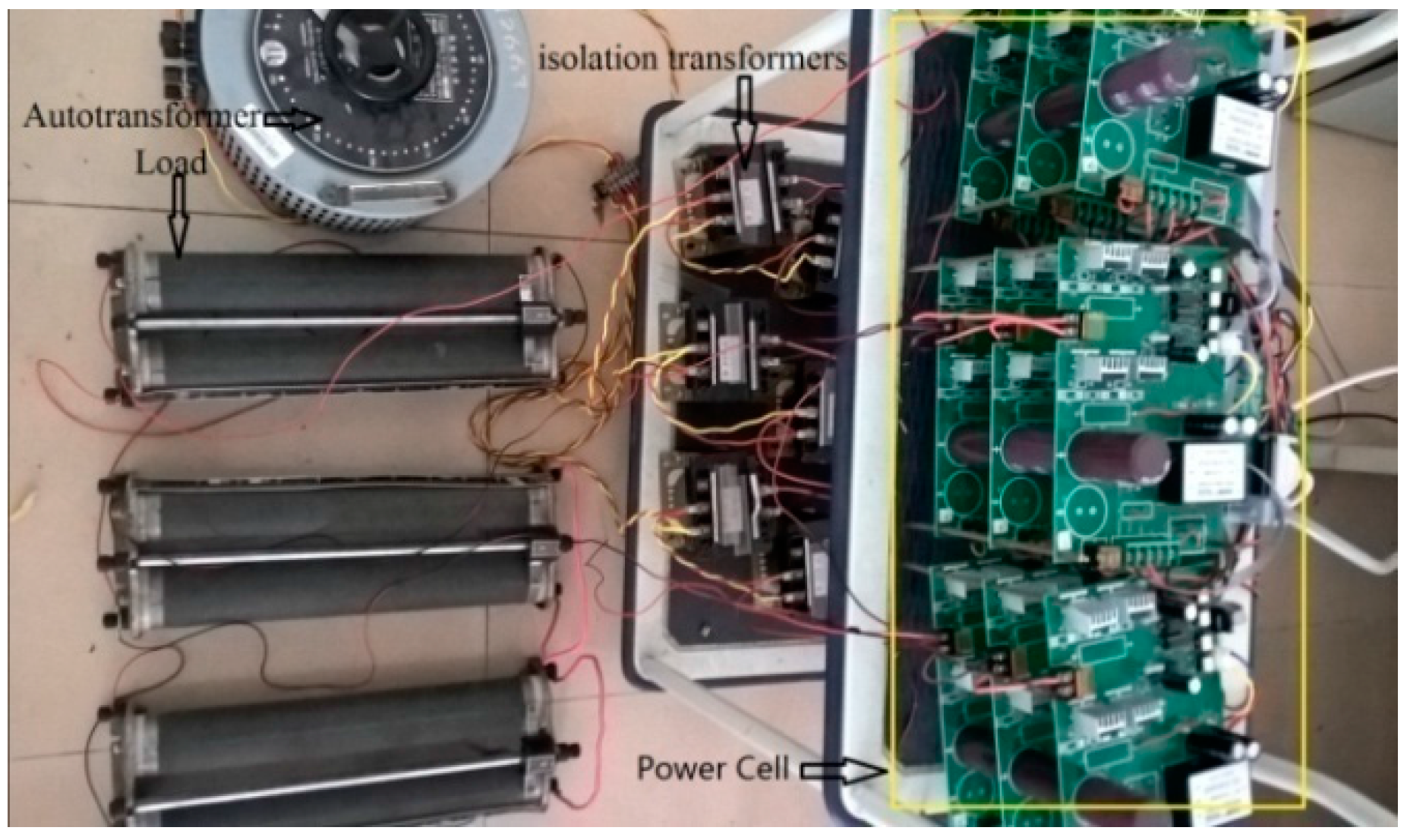
A 7-level cascaded multilevel inverter is built in the laboratory, as shown in Figure 17. Nine isolation DC power for the 7-level inverter are formed by nine 200 W isolation transformers and diode rectifier bridges. The dc-bus voltage of power cells is selected as 50 V. The model of switches in the inverter is IRFP460, and the driver circuits are composed of high-speed opt- coupler (model: 6N137) and IR2110. The inverter is controlled by a TMS320F28335 floating-point DSP from Texas Instruments (Dallas, TX, USA). The experimental setup is shown in Figure 18.
4.2. Experimental Results
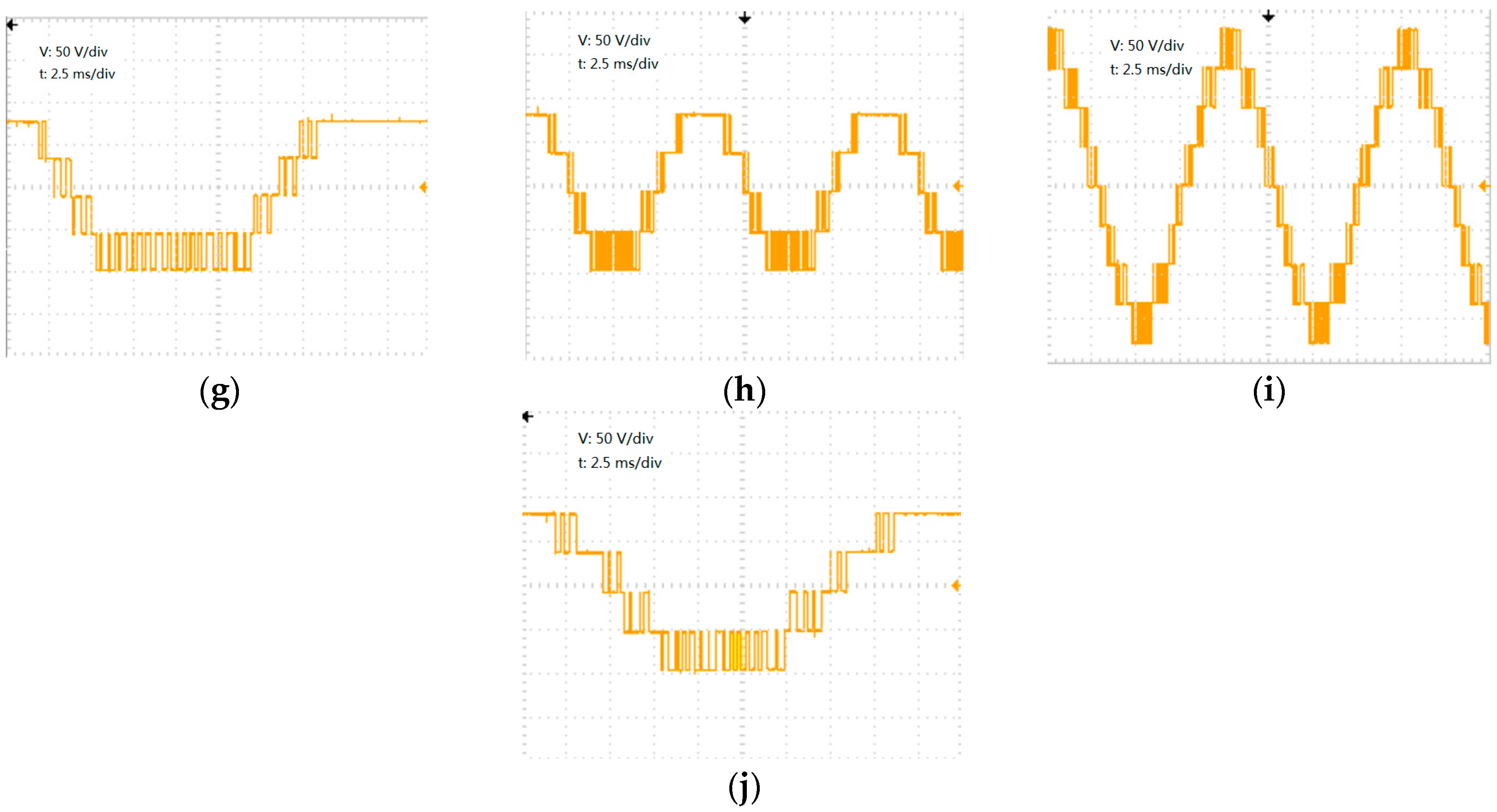
The waveforms of the 7- level inverter with different modulation indexes are shown in Figure 19. Where, the fundamental frequency of output voltage is set to be 100 Hz.
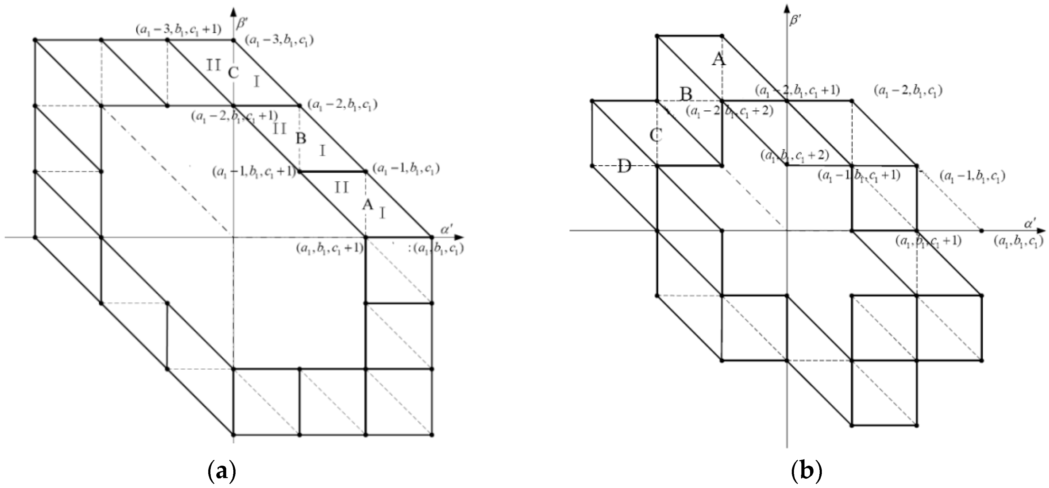
As seen from Figure 19e,j, the phase voltage is kept at the highest level for some time without changing. The corresponding graph on uncharged parts of the phase voltage A and the traversing graph is illustrated in Figure 20.
As shown in Figure 20, there is no diagonal switching mode in the magenta region. Hence, the phase voltage A remains unchanged. The similar conclusions can be obtained in the yellow region and the blue region. For simplicity, we choose 5-level inverter to analyze the number of commutations of switches for different switching paths.
There are two traversing graphs when the reference voltage are in the outermost layer, and the switching paths for the two traversing graphs are shown in Figure 21. Where, solid lines stand for the feasible basic switching modes, and dotted lines are the forbidden basic switching modes.
If interface vector ① is chosen as the starting vector, the number of commutations of switches is 2Mj in a quadrilateral. Where, Mj = Mj1 + Mj2. Mj1 and Mj2 are the number of sampling points in △A and △B, respectively. If the starting vector of current quadrilateral and the ending vector of previous quadrilateral are the same vector, an extra switching modes need to be added. Therefore, the maximum number of commutations of switches for the first class switching path is:
where, Mj = Mj1 + Mj2, and J is the number of quadrilateral.
With the above statistical method, the maximum number of commutations of switches for the second class switching path can be calculated as:
Table 5 lists the number of commutations of switches for 5-level inverter in the first class switching paths shown in Figure 20a.
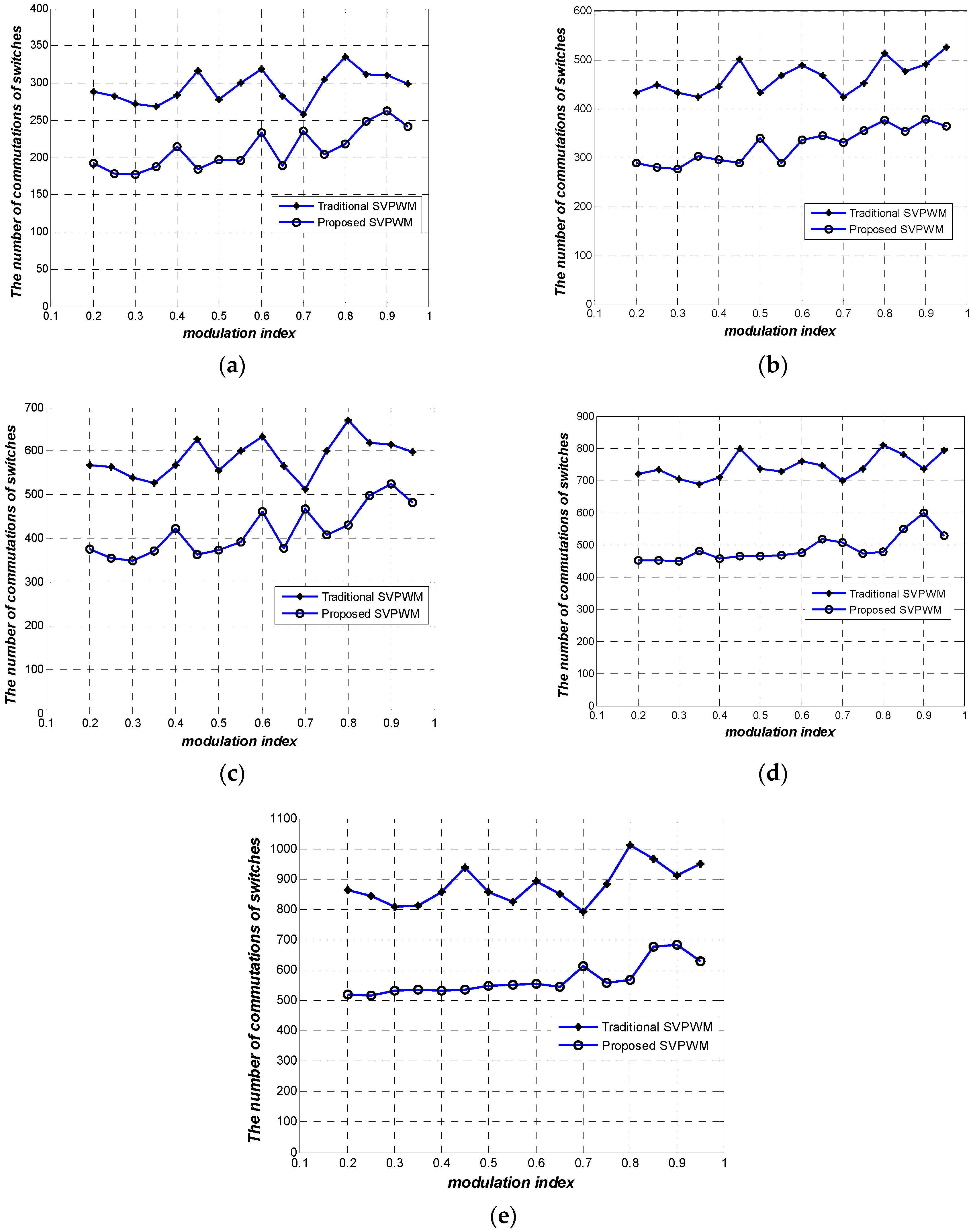
As shown in Table 5, the actual number of commutations of switches is consistent with the theoretical calculation. The numbers of commutations of switches in one period with different number of sampling points by the proposed SVPWM scheme and the classical SVPWM scheme are shown in Figure 22. Where, the same realizations of all vectors are used by classical SVPWM scheme.
As shown in Figure 22, the average difference in terms of the number of commutations of switches is about 45% between the traditional SVPWM scheme and the proposed SVPWM scheme, which confirms the effectiveness of the proposed method in decreasing the number of commutations of switches.
Because all switching paths are comprised of the three switching modes, only one phase voltage limited in 1 pu is achieved. Compared to other PWM schemes [25,26,27], the proposed SVPWM scheme is also an effective way to decrease the di/dt of the output current and dV/dt of the output voltage for multilevel inverters as well as reduce the switching losses of switches.
4.3. Compared with Other PWM Schemes
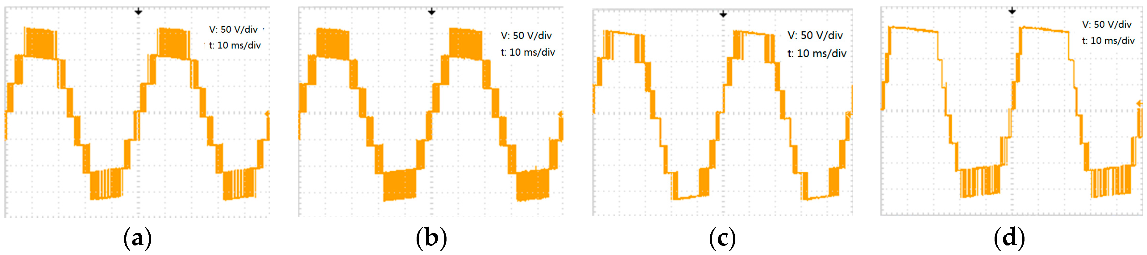
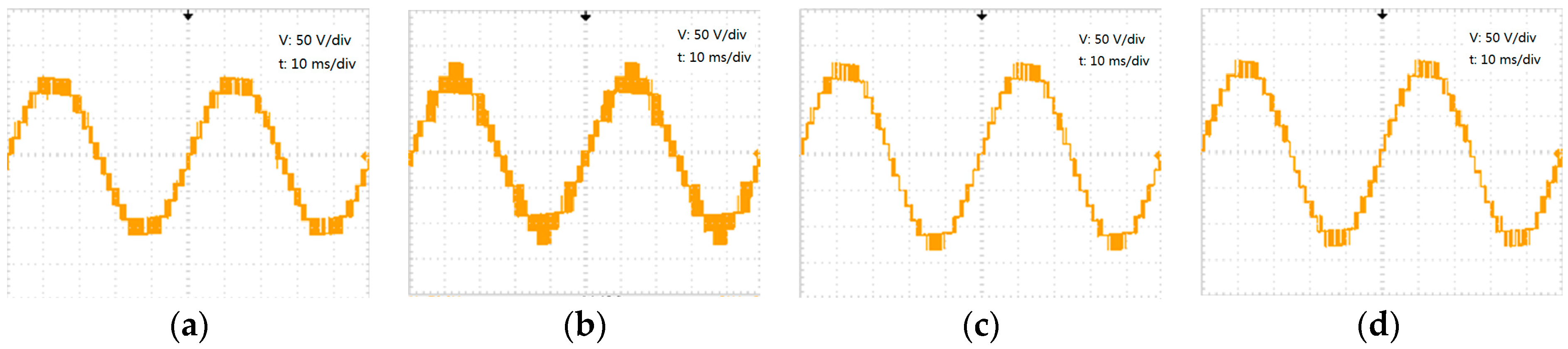
Phase voltage and line-to-line voltage waveforms with in-phase disposition PWM (IPDPWM) scheme, phase shifted PWM (PSPWM) scheme, classical SVPWM scheme and proposed SVPWM scheme are shown in Figure 23 and Figure 24, respectively. Where, the fundamental frequency of output voltage is 20 Hz. The modulation index m = 0.94, and the carrier frequency or the sampling frequency for these PWM schemes is 4200 Hz.
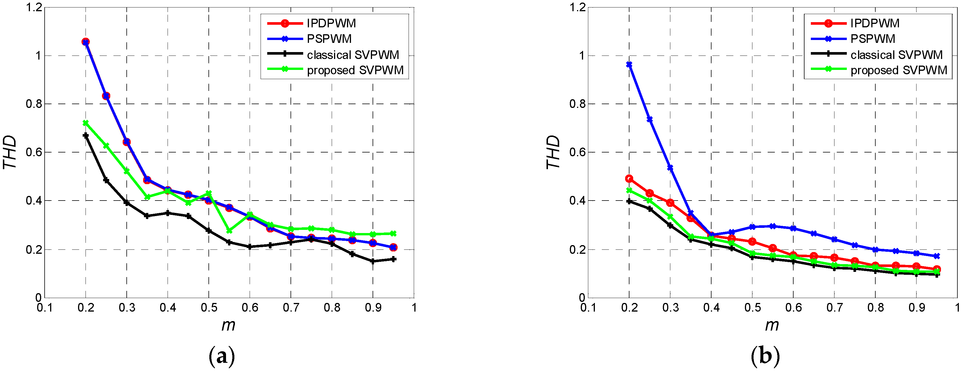
The THDs of phase voltage and line-to-line voltage of the multilevel inverter with different modulation indexes for the four PWM schemes are shown in Figure 25.
As IPDPWM scheme and PSPWM scheme belong to carrier modulation scheme, the THDs of phase voltage and line-to-line voltage with the two PWM schemes are higher than these of the other scheme. Because phase voltage is kept constant for some time to decrease the number of commutations of the switches in the proposed SVPWM scheme, the THDs of phase voltage with the proposed SVPWM scheme is higher than these of classical SVPWM scheme. However, the THDs of line-to-line voltage with the proposed SVPWM scheme is similar to these of classical SVPWM scheme. This is because that the proposed SVPWM scheme is derived from classical SVPWM scheme. As shown in Figure 25, the THD difference between the proposed SVPWM scheme and the classical SVPWM scheme is about 1.2%. Hence, if the proposed SVPWM scheme is used in motor speed control system, the time response of the rotor speed is slightly lower than that of the classical SVPWM scheme.
5. Conclusions
This paper proposes a novel switching frequency optimized SVPWM. The proposed SVPWM is developed in a α′β′ coordinate system. By planning the switching paths, only one phase voltage limited in dc-bus voltage of power cells is achieved. The experimental results show that the proposed method significantly outperforms the traditional SVPWM in terms of decreasing the number of commutations of switches.
Acknowledgments
This work was supported by Guangdong Provincial Science and Technology Project under grant number 2015B020238013, and Guangdong Provincial Natural Science Foundation Project under grant number 2015A030313487.
Author Contributions
Xiongmin Tang wrote the paper and performed the experimental work; Junhui Zhang contributed to the writing and arranging of the analytical data; Zheng Liu contributed to perform the simulation work. Miao Zhang contributed to providing reagents/materials/analysis tools and supervised the paper.
Conflicts of Interest
The authors declare no conflict of interest.
References
- Rodriguez, J.; Lai, J.S.; Peng, F.Z. Multilevel inverters: A survey of topologies, controls, and applications. IEEE Trans. Ind. Electron. 2002, 49, 724–738. [Google Scholar] [CrossRef]
- Cai, X.J.; Wu, Z.X.; Wang, S.X. Phase-Shifted Carrier Pulse Width Modulation Based on Particle Swarm Optimization for Cascaded H-bridge Multilevel Inverters with Unequal DC Voltages. Energies 2015, 8, 9670–9687. [Google Scholar] [CrossRef]
- Patil, U.V.; Suryawanshi, H.M.; Renge, M.M. Closed-loop hybrid direct torque control for medium voltage induction motor drive for performance improvement. IET Power Electron. 2014, 7, 31–40. [Google Scholar] [CrossRef]
- Stefan, P.E.; Marco, S.; Nils, S.; Sedigheh, R.; Hanno, S.; Rik, W.D.D. Comparison of the modular multilevel DC Converter and the dual-active bridge converter for power conversion in HVDC and MVDC grids. IEEE Trans. Power Electron. 2015, 30, 124–137. [Google Scholar] [CrossRef]
- Ravikant, P.; Tripathi, R.N.; Hanamoto, T. Comprehensive analysis of LCL filter interfaced cascaded h-bridge multilevel inverter-based DSTATCOM. Energies 2017, 10, 346. [Google Scholar] [CrossRef]
- Zhu, H.F.; Shu, Z.L.; Qin, B.; Gao, S.B. Five-level diode-clamped active power filter using voltage space vector-based indirect current and predictive harmonic control. IET Power Electron. 2014, 7, 713–723. [Google Scholar] [CrossRef]
- Parastar, A.; Kuan, Y.C.; Seok, J.K. Multilevel modular dc/dc power converter for high-voltage dc-connected offshore wind energy applications. IEEE Trans. Ind. Electron. 2015, 62, 2879–2890. [Google Scholar] [CrossRef]
- Essakiappan, S.; Krishnamoorthy, H.S.; Enjeti, P.; Balog, R.S.; Ahmed, S. Multilevel medium-frequency link inverter for utility scale photovoltaic integration. IEEE Trans. Power Electron. 2015, 30, 3674–3684. [Google Scholar] [CrossRef]
- Sadigh, A.K.; Dargahi, V.; CorzineK, A. Analytical determination of conduction and switching power losses in flying-capacitor-based active neutral-point-clamped multilevel converter. IEEE Trans. Power Electron. 2016, 31, 5473–5494. [Google Scholar] [CrossRef]
- Wang, H.; Zhang, D.L.; Wang, Y.; Wu, B.; Athab, H.S. Power and voltage balance control of a novel three-phase solid-state transformer using multilevel cascaded h-bridge inverters for microgrid applications. IEEE Trans. Power Electron. 2016, 31, 3289–3301. [Google Scholar] [CrossRef]
- Mehrasa, M.; Pouresmaeil, E.; Zabihi, S.; Caballero, J.C.T.; Catalão, J.P.S. A novel modulation function-based control of modular multilevel converters for high voltage direct current transmission systems. Energies 2016, 9, 867. [Google Scholar] [CrossRef]
- Li, X.; Akin, S.D.B.; Rajashekara, K. A new active fault-tolerant SVPWM strategy for single-phase faults in three-phase multilevel converters. IEEE Trans. Ind. Electron. 2015, 62, 3955–3965. [Google Scholar] [CrossRef]
- Jana, K.C.; Biswas, S.K. Generalised switching scheme for a space vector pulse-width modulation-based N-level inverter with reduced switching frequency and harmonics. IET Power Electron. 2015, 8, 2377–2385. [Google Scholar] [CrossRef]
- Moranchel, M.; Huerta, F.; Sanz, I.; Bueno, E.; Rodríguez, F.J. A Comparison of modulation techniques for modular multilevel converters. Energies 2016, 9, 1091. [Google Scholar] [CrossRef]
- Dekka, A.; Wu, B.; Zargari, N.R.; Fuentes, R.L. A space-vector PWM-based voltage-balancing approach with reduced current sensors for modular multilevel converter. IEEE Trans. Ind. Electron. 2016, 63, 2734–2745. [Google Scholar] [CrossRef]
- Lopez, O.; Alvarez, J.; Malvar, J.; Yepes, A.G.; Vidal, A.; Baneira, F.; Estevez, D.P.; Freijedo, F. Space vector PWM with common-mode voltage elimination for multiphase drives. IEEE Trans. Power Electron. 2016, 31, 8151–8161. [Google Scholar] [CrossRef]
- Liu, Z.; Wang, Y.; Tan, G.J.; Li, H.; Zhang, Y.F. A novel SVPWM algorithm for five-level active neutral-point-clamped converter. IEEE Trans. Power Electron. 2016, 31, 3859–3866. [Google Scholar] [CrossRef]
- Rodríguez, J.; Morán, L.; Pontt, J.; Correa, P.; Silva, C. A high-performance vector control of an 11-level Inverter. IEEE Trans. Ind. Electron. 2003, 50, 80–85. [Google Scholar] [CrossRef]
- Celanovic, N.; Boroyevich, D. A fast space vector modulation algorithm for multilevel three phase converters. IEEE Trans. Ind. Appl. 2001, 37, 637–641. [Google Scholar] [CrossRef]
- Carnielutti, F.; Pinheiro, H. Hybrid modulation strategy for asymmetrical cascaded multilevel converters under normal and fault conditions. IEEE Trans. Ind. Electron. 2016, 63, 92–101. [Google Scholar] [CrossRef]
- Carnielutti, F.; Rech, C.; Pinheiro, H. Space vector modulation for cascaded asymmetrical multilevel converters under fault conditions. IEEE Trans. Ind. Appl. 2015, 51, 344–352. [Google Scholar] [CrossRef]
- Sozer, Y.; Torrey, D.A.; Saha, A.; Nguyen, H.; Hawes, N. Fast minimum loss space vector pulse-width modulation algorithm for multilevel inverters. IET Power Electron. 2014, 7, 1590–1602. [Google Scholar] [CrossRef]
- Deng, Y.; Teo, K.H.; Duan, C.; Habetler, T.G.; Harley, R.G. A fast and generalized space vector modulation scheme for multilevel inverters. IEEE Trans. Power Electron. 2014, 29, 5204–5217. [Google Scholar] [CrossRef]
- Wang, C.; Zhang, Y.; Tang, X.M.; Cheng, S.Z. Rapid and generalised space vector modulation algorithm for cascaded multilevel converter based on zero-order voltage constraint. IET Power Electron. 2016, 9, 989–996. [Google Scholar] [CrossRef]
- Yao, W.; Hu, H.; Lu, Z. Comparisons of space-vector modulation and carrier-based modulation of multilevel inverter. IEEE Trans. Power Electron. 2008, 23, 45–51. [Google Scholar] [CrossRef]
- Lim, Y.C.; Wi, S.O.; Kim, J.N.; Jung, Y.G. A pseudorandom carrier modulation scheme. IEEE Trans. Power Electron. 2010, 25, 797–805. [Google Scholar] [CrossRef]
- Boonmee, C.; Wajanatepin, N. Comparison of using carrier-based pulse width modulation techniques for cascaded h-bridge inverters application in the PV energy systems. In Proceedings of the International Electrical Engineering Congress, Chonburi, Thailand, 19–21 March 2014; pp. 1–4. [Google Scholar] [CrossRef]
Figure 1.
Space vector diagram for 3-level inverter in different coordinate systems, (a) in the traditional αβ coordinate system (b) in the α′β′ coordinate system.
Figure 1.
Space vector diagram for 3-level inverter in different coordinate systems, (a) in the traditional αβ coordinate system (b) in the α′β′ coordinate system.

Figure 2.
Locus of three basic switching modes.
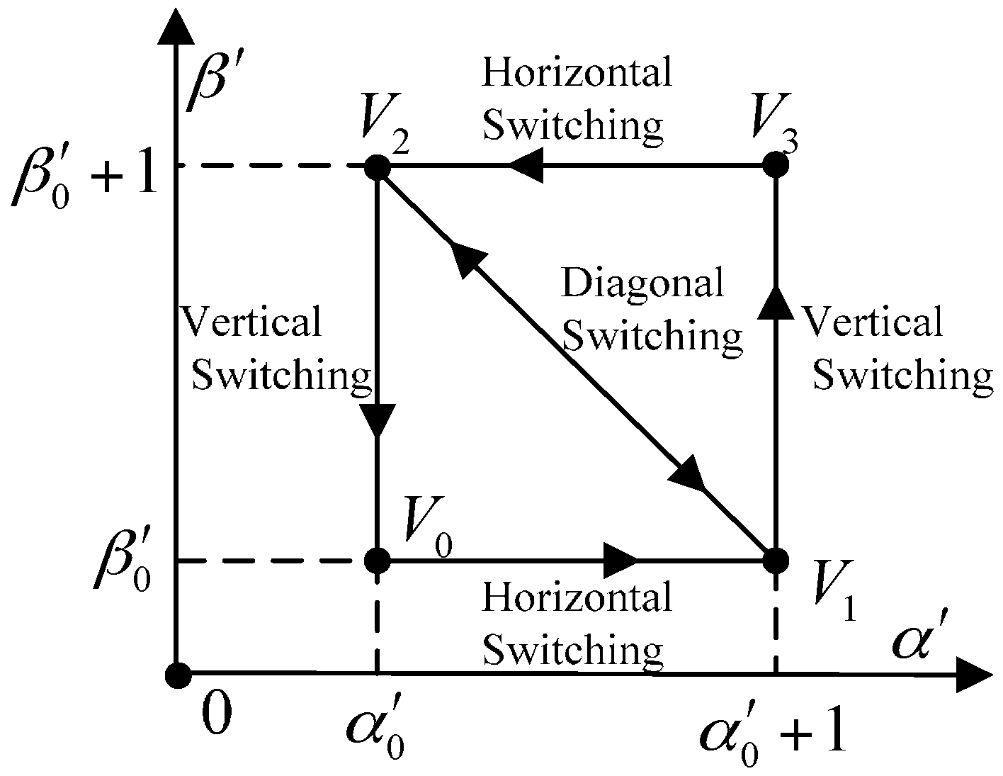
Figure 3.
Three kinds of quadrangles, (a) the first kind; (b) the second kind; (c) the third kind.
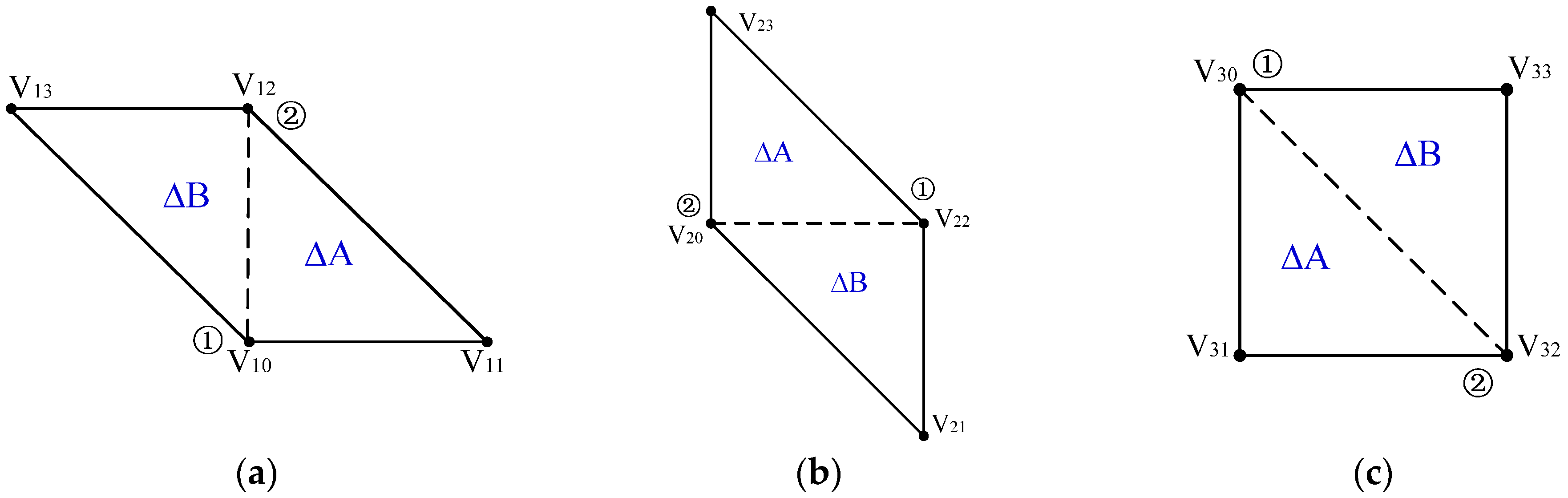
Figure 4.
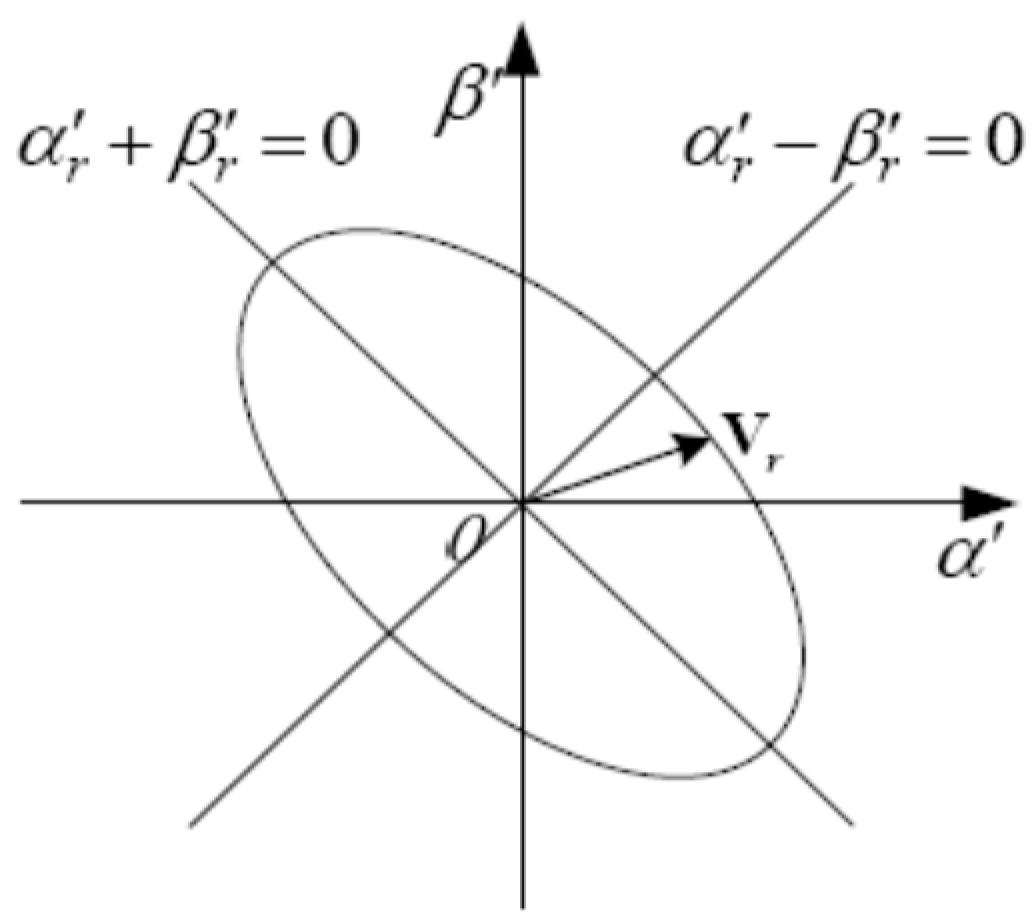
Trajectory of Vr.

Figure 5.
Traversing graphs of reference voltage vector with different modulation indexes for 7-level inverter, (a) 0.9632 < m < 1; (b) 0.8819 < m < 0.9632; (c) 0.8333 < m < 0.8819.
Figure 5.
Traversing graphs of reference voltage vector with different modulation indexes for 7-level inverter, (a) 0.9632 < m < 1; (b) 0.8819 < m < 0.9632; (c) 0.8333 < m < 0.8819.
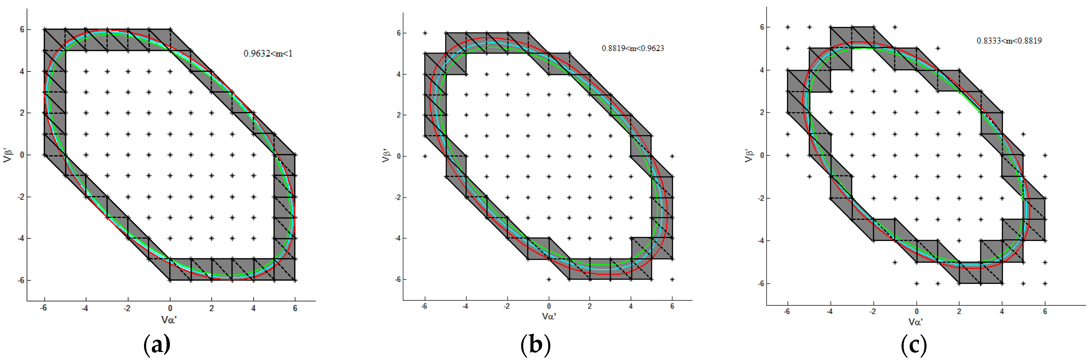
Figure 6.
Switching paths in the first kind of quadrangle, (a) state 1; (b) state 2; (c) state 3; (d) state 4.
Figure 6.
Switching paths in the first kind of quadrangle, (a) state 1; (b) state 2; (c) state 3; (d) state 4.

Figure 7.
Switching paths in the second kind of quadrangle, (a) state 1; (b) state 2; (c) state 3; (d) state 4.
Figure 7.
Switching paths in the second kind of quadrangle, (a) state 1; (b) state 2; (c) state 3; (d) state 4.

Figure 8.
Switching paths in the third kind of quadrangle, (a) state 1; (b) state 2; (c) state 3; (d) state 4.
Figure 8.
Switching paths in the third kind of quadrangle, (a) state 1; (b) state 2; (c) state 3; (d) state 4.
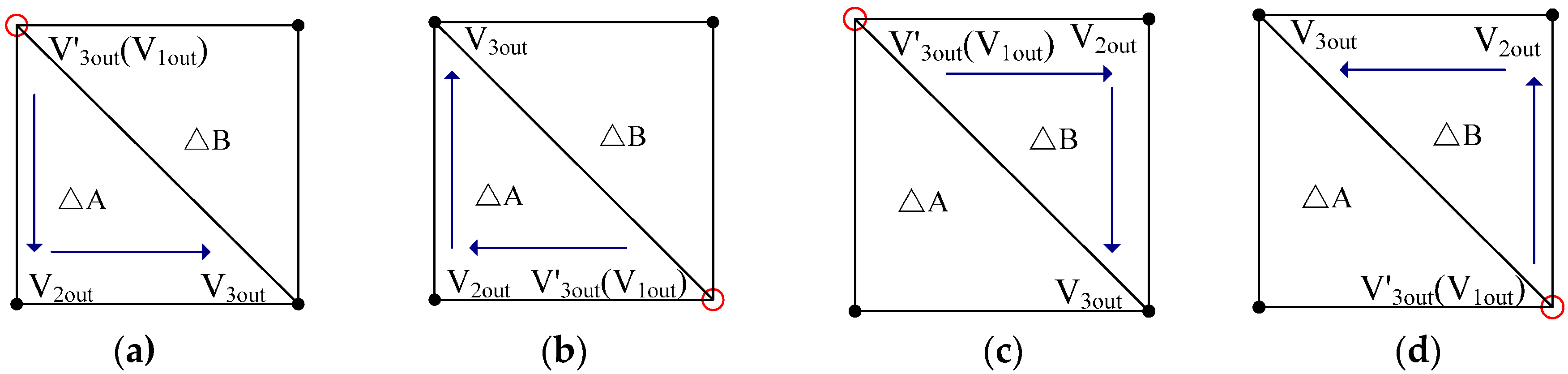
Figure 9.
Switching paths in the first kind of quadrangle, (a) state 1; (b) state 2.
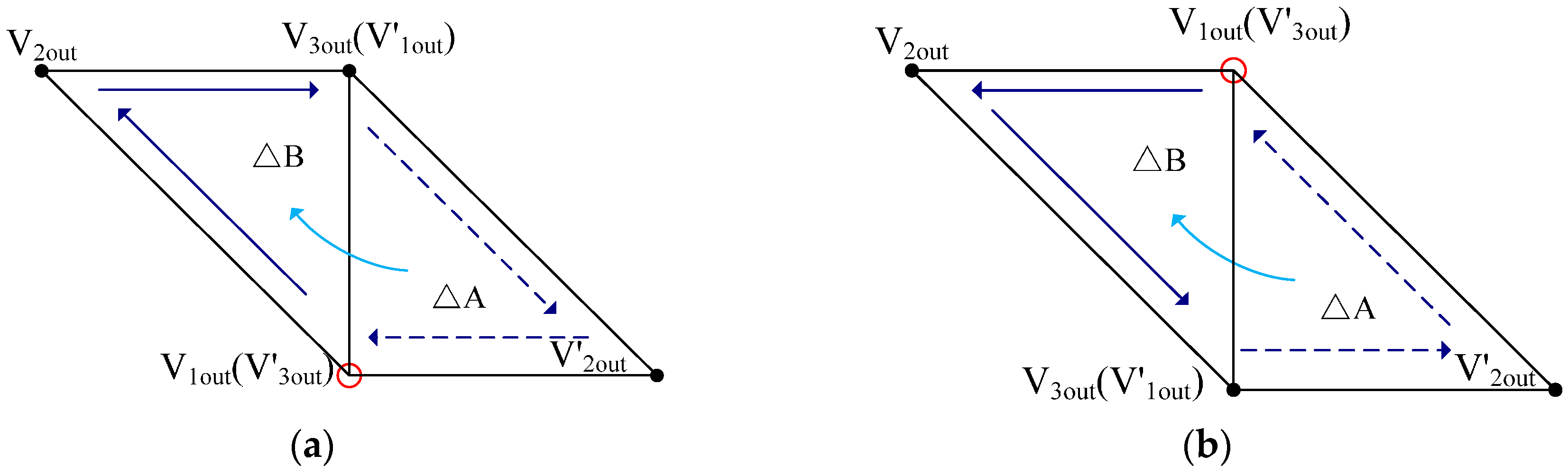
Figure 10.
Switching paths in the second kind of quadrangle, (a) state 1; (b) state 2.

Figure 11.
Switching paths in the third kind of quadrangle, (a) state 1; (b) state 2.

Figure 12.
Transition graphs between different kinds of quadrilaterals, (a) the first kind of quadrilateral; (b) the second kind of quadrilateral; (c) the third kind of quadrilateral.
Figure 12.
Transition graphs between different kinds of quadrilaterals, (a) the first kind of quadrilateral; (b) the second kind of quadrilateral; (c) the third kind of quadrilateral.
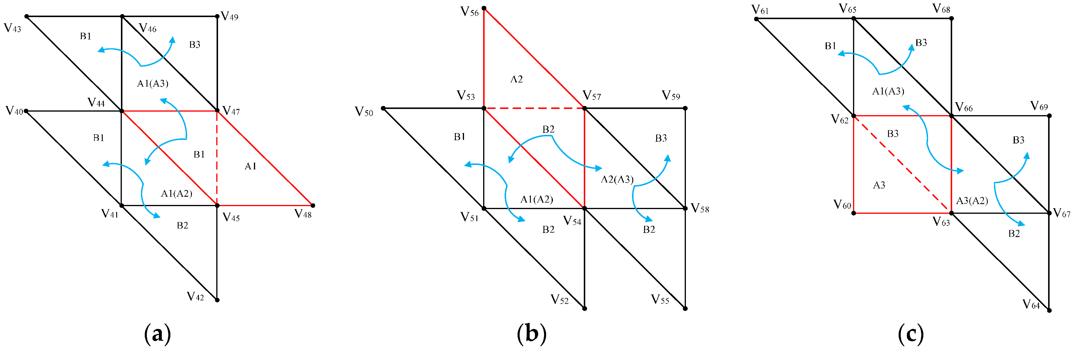
Figure 13.
Space vector diagram with three zones.

Figure 14.
Realization of vector (2, −1).
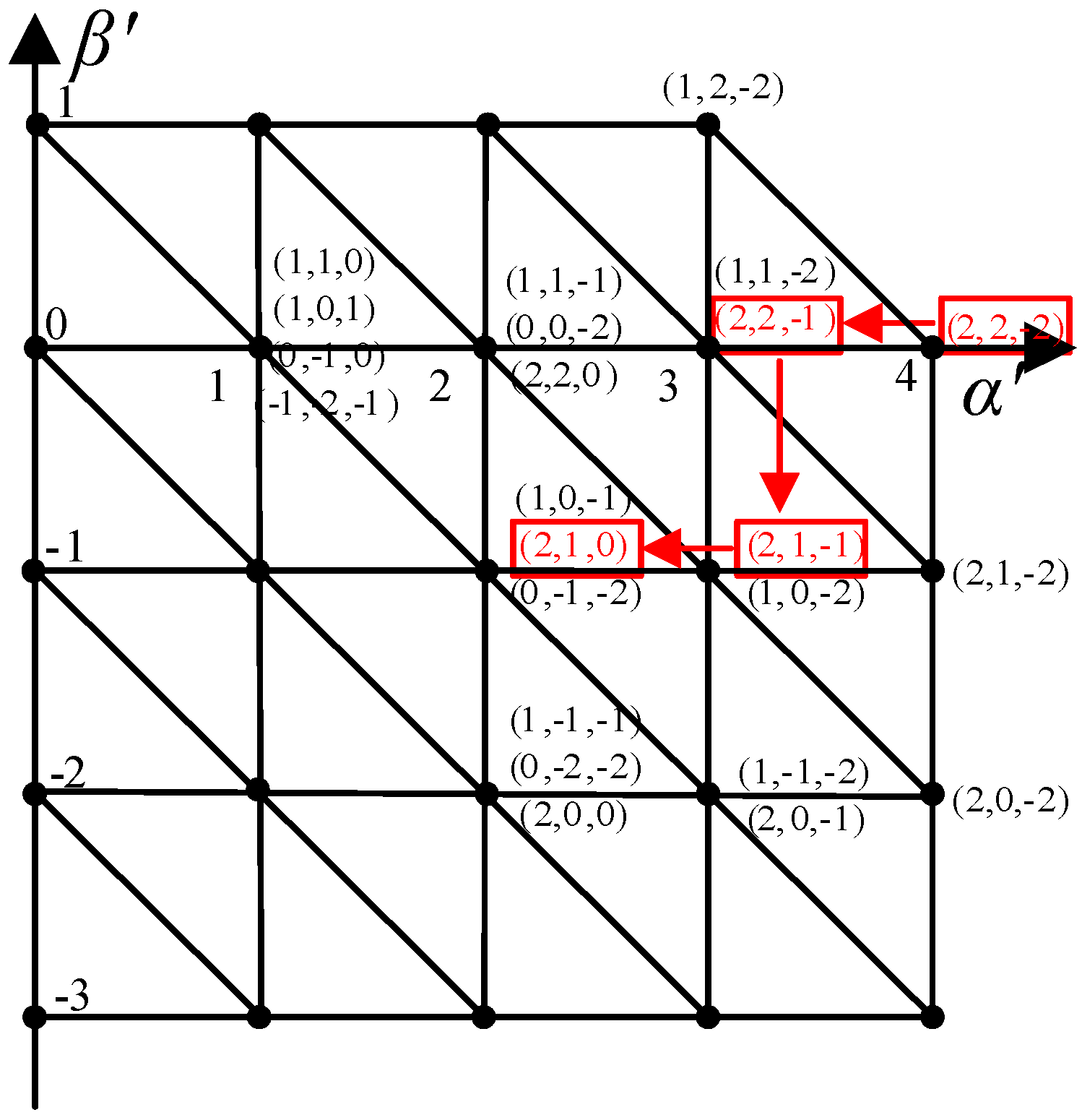
Figure 15.
Realization of other vectors, (a) in the first kind of quadrilateral; (b) in the second kind of quadrilateral; (c) in the third kind of quadrilaterals.
Figure 15.
Realization of other vectors, (a) in the first kind of quadrilateral; (b) in the second kind of quadrilateral; (c) in the third kind of quadrilaterals.
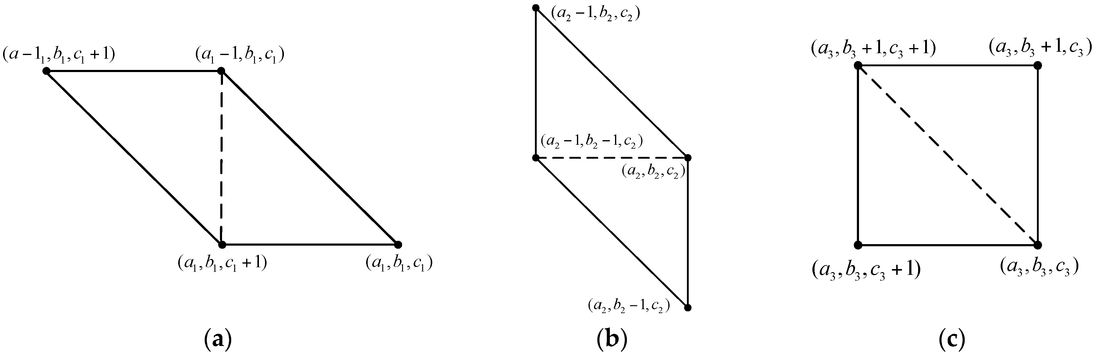
Figure 16.
Flowchart of the implementation of the SVPWM scheme.
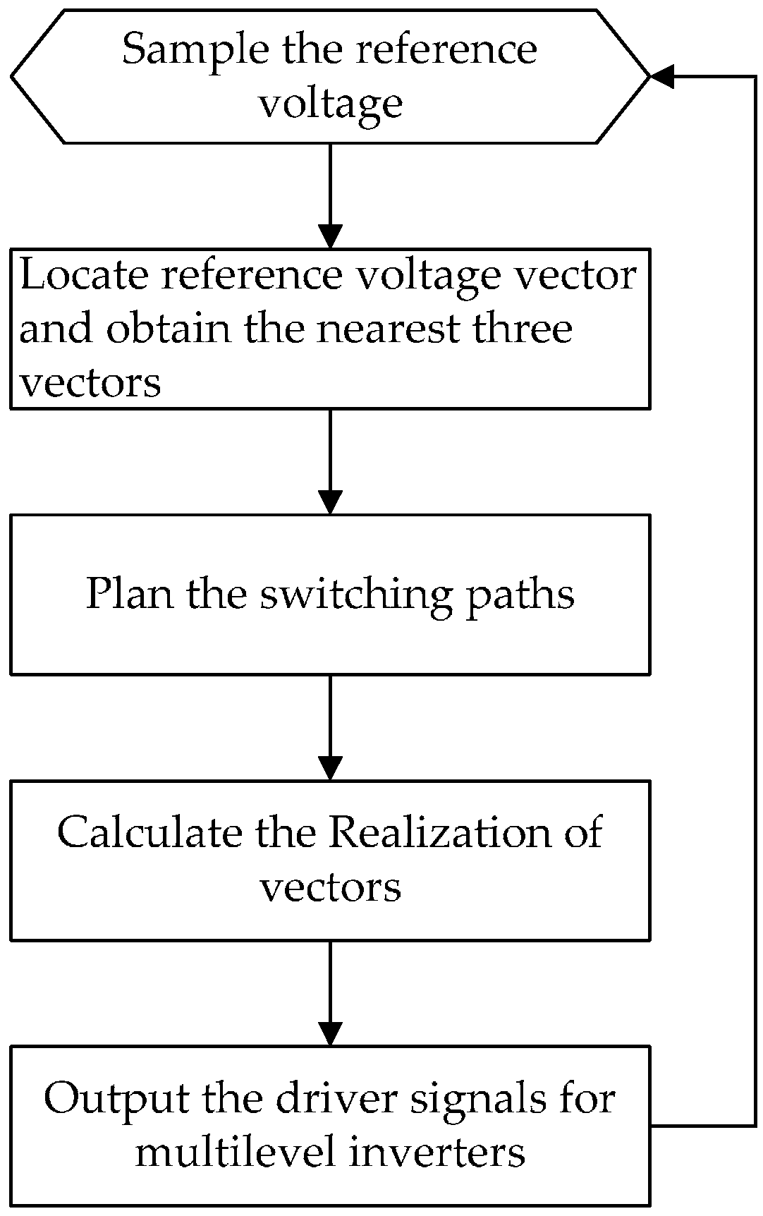
Figure 17.
7-level cascaded multilevel inverter.
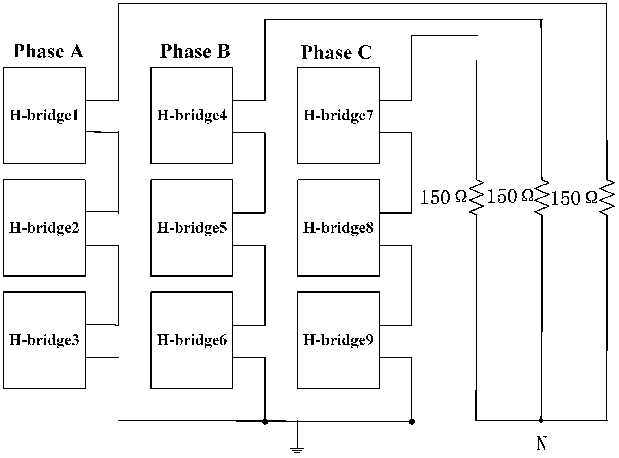
Figure 18.
Experimental setup.

Figure 19.
Waveforms of the 7-level inverter, (a) phase voltage A with m = 0.981; (b) line-to-line voltage AB with m = 0.981; (c) phase voltage A with m = 0.922; (d) line-to-line voltage AB with m = 0.922; (e) phase voltage A with m = 0.75; (f) details of the waveform in (f); (g) phase voltage A with m = 0.665; (h) phase voltage A with m = 0.665; (i) line-to-line voltage AB with m = 0.665; (j) details of the waveform in (j).
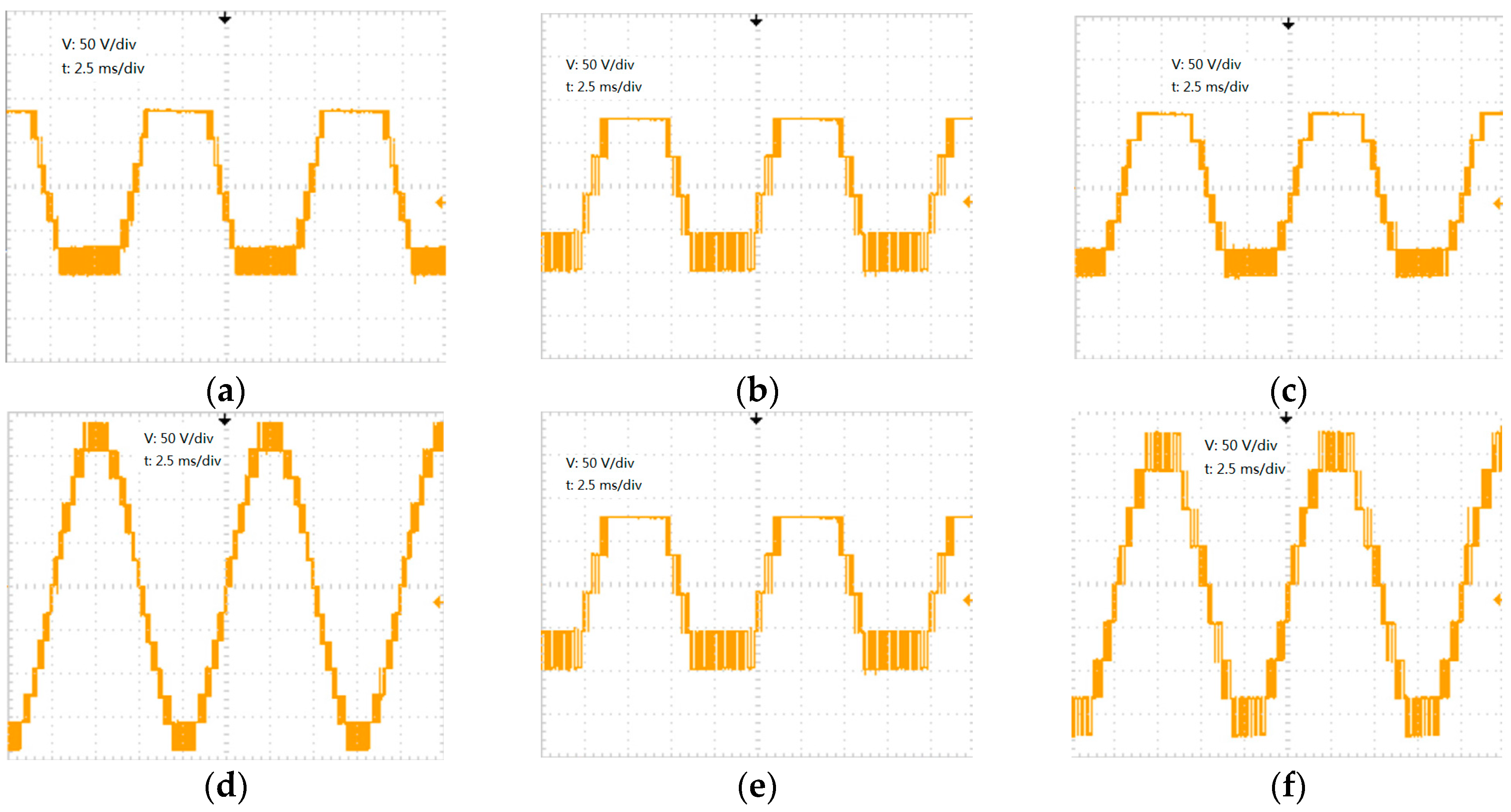

Figure 20.
Corresponding graph on unchanged parts of the phase voltage A and traversing graph.

Figure 21.
Switching paths for 5-level inverter in the outermost layer, (a) the first class switching path, (b) the second class switching path.
Figure 21.
Switching paths for 5-level inverter in the outermost layer, (a) the first class switching path, (b) the second class switching path.

Figure 22.
Numbers of commutations of switches with different number of sampling points in one period, (a) 42 sampling points; (b) 64 sampling points; (c) 84 sampling points; (d) 105 sampling points; (e) 126 sampling points.
Figure 22.
Numbers of commutations of switches with different number of sampling points in one period, (a) 42 sampling points; (b) 64 sampling points; (c) 84 sampling points; (d) 105 sampling points; (e) 126 sampling points.

Figure 23.
Phase voltage of 7-level inverter with different PWM schemes, (a) IPDPWM; (b) PSPWM; (c) classical SVPWM; (d) proposed SVPWM.
Figure 23.
Phase voltage of 7-level inverter with different PWM schemes, (a) IPDPWM; (b) PSPWM; (c) classical SVPWM; (d) proposed SVPWM.

Figure 24.
Line-to-line voltage of 7-level inverter with different PWM schemes, (a) IPDPWM; (b) PSPWM; (c) classical SVPWM; (d) proposed SVPWM.
Figure 24.
Line-to-line voltage of 7-level inverter with different PWM schemes, (a) IPDPWM; (b) PSPWM; (c) classical SVPWM; (d) proposed SVPWM.

Figure 25.
THDs of phase voltage and line-to- line voltage of 5-level inverter with different PWM schemes, (a) phase voltage; (b) line-to-line voltage.
Figure 25.
THDs of phase voltage and line-to- line voltage of 5-level inverter with different PWM schemes, (a) phase voltage; (b) line-to-line voltage.


Table 1.
Three basic switching modes.
| Switching Mode | ∆a | ∆b | ∆c | ∆α′ | ∆β′ |
|---|---|---|---|---|---|
| diagonal | ±1 | 0 | 0 | ±1 | ∓1 |
| vertical | 0 | ±1 | 0 | 0 | |
| horizontal | 0 | 0 | ±1 | ∓1 | 0 |
Table 2.
Feasible switching paths between the first kind and other kinds of quadrilaterals.
| Adjacent Quadrilateral | Starting Vector | Switching Path | Note |
|---|---|---|---|
| the first kind of quadrilateral | V47 | V47→V44→V47→V46 | B1 into A1(A3) |
| V45 | V45→V44→V47→V46 | B1 into A1(A3) | |
| the first kind of quadrilateral | V47 | V47→V44→V45→V41 | B1 into A1(A2) |
| V45 | V45→V41→V45→V44 | B1 into A1(A2) | |
| the second kind of quadrilateral | V47 | V47→V44→V45→V44→V41 | B1 into A1(A2) |
| V45 | V45→V44→V41 | B1 into A1(A2) | |
| the third kind of quadrilateral | V47 | V47→V44→V46 | B1 into A1(A3) |
| V45 | V45→V44→V47→V44→V46 | B1 into A1(A3) |
Table 3.
Feasible switching paths between the second kind and other kinds of quadrilateral.
| Adjacent Quadrilateral | Starting Vector | Switching Path | Note |
|---|---|---|---|
| the first kind of quadrilateral | V57 | V57→V54→V53→V54→V52 | B2 into A1(A2) |
| V53 | V53→V54→V51 | B2 into A1(A3) | |
| the second kind of quadrilateral | V57 | V57→V54→V53→V51 | B2 into A1(A2) |
| V53 | V53→V54→V53→V54 | B2 into A1(A2) | |
| the second kind of quadrilateral | V57 | V57→V54→V57→V58 | B2 into A2(A3) |
| V53 | V53→V54→V57→V58 | B2 into A2(A3) | |
| the third kind of quadrilateral | V57 | V57→V54→V58 | B2 into A1(A3) |
| V53 | V53→V54→V57→V54→V58 | B2 into A1(A3) |
Table 4.
Feasible switching paths between the third kind and other kinds of quadrilateral.
| Adjacent Quadrilateral | Starting Vector | Switching Path | Note |
|---|---|---|---|
| the first kind of quadrilateral | V62 | V62→V66→V65 | B3 into A1(A3) |
| V63 | V63→V66→V62→V66→V65 | B3 into A1(A3) | |
| the second kind of quadrilateral | V62 | V62→V66→V63→V66→V67 | B3 into A3(A2) |
| V63 | V63→V66→V67 | B3 into A3(A2) | |
| the third kind of quadrilateral | V62 | V62→V66→V63→V67 | B3 into A3(A2) |
| V63 | V63→V66→V63→V67 | B3 into A3(A2) | |
| the third kind of quadrilateral | V62 | V62→V66→V62→V65 | B3 into A1(A3) |
| V63 | V63→V66→V62→V65 | B3 into A1(A3) |
Table 5.
Number of commutations of switches for 5-level inverter.
| Number of Sampling Points in One Period | Maximum Number from Theoretical Calculation (Times) | Experimental Results (Times) |
|---|---|---|
| 42 | 108 | 103 |
| 63 | 150 | 149 |
| 84 | 192 | 190 |
© 2017 by the authors. Licensee MDPI, Basel, Switzerland. This article is an open access article distributed under the terms and conditions of the Creative Commons Attribution (CC BY) license (http://creativecommons.org/licenses/by/4.0/).
Share and Cite
MDPI and ACS Style
Tang, X.; Zhang, J.; Liu, Z.; Zhang, M. A Switching Frequency Optimized Space Vector Pulse Width Modulation (SVPWM) Scheme for Cascaded Multilevel Inverters. Energies 2017, 10, 725. https://doi.org/10.3390/en10050725
AMA Style
Tang X, Zhang J, Liu Z, Zhang M. A Switching Frequency Optimized Space Vector Pulse Width Modulation (SVPWM) Scheme for Cascaded Multilevel Inverters. Energies. 2017; 10(5):725. https://doi.org/10.3390/en10050725
Chicago/Turabian StyleTang, Xiongmin, Junhui Zhang, Zheng Liu, and Miao Zhang. 2017. "A Switching Frequency Optimized Space Vector Pulse Width Modulation (SVPWM) Scheme for Cascaded Multilevel Inverters" Energies 10, no. 5: 725. https://doi.org/10.3390/en10050725
Note that from the first issue of 2016, this journal uses article numbers instead of page numbers. See further details here.