A New Combined Boost Converter with Improved Voltage Gain as a Battery-Powered Front-End Interface for Automotive Audio Amplifiers


1
Department of Vehicle Engineering, National Taipei University of Technology, 1, Sec. 3, Chung-Hsiao E. Road, Taipei 106, Taiwan
2
Department of Information and Communication Engineering, Chaoyang University of Technology, Taichung 41349, Taiwan
3
School of Electrical and Electronic Engineering, Universiti Sains Malaysia, USM Engineering Campus, Nibong Tebal, Seberang Perai Selatan 14300, Penang, Malaysia
4
Department of Electrical Engineering, National Taiwan University, No. 1, Sec. 4, Roosevelt Rd., Taipei 106, Taiwan
*
Author to whom correspondence should be addressed.
Energies 2017, 10(8), 1128; https://doi.org/10.3390/en10081128
Submission received: 18 April 2017
/
Revised: 4 June 2017
/
Accepted: 28 July 2017
/
Published: 1 August 2017
(This article belongs to the Special Issue Energy Management, Control, and System Architectures for Electric Vehicle Applications)
Abstract
:High boost DC/DC voltage conversion is always indispensable in a power electronic interface of certain battery-powered electrical equipment. However, a conventional boost converter works for a wide duty cycle for such high voltage gain, which increases power consumption and has low reliability problems. In order to solve this issue, a new battery-powered combined boost converter with an interleaved structure consisting of two phases used in automotive audio amplifier is presented. The first phase uses a conventional boost converter; the second phase employs the inverted type. With this architecture, a higher boost voltage gain is able to be achieved. A derivation of the operating principles of the converter, analyses of its topology, as well as a closed-loop control designs are performed in this study. Furthermore, simulations and experiments are also performed using input voltage of 12 V for a 120 W circuit. A reasonable duty cycle is selected to reach output voltage of 60 V, which corresponds to static voltage gain of five. The converter achieves a maximum measured conversion efficiency of 98.7% and the full load efficiency of 89.1%.
1. Introduction
High boost DC/DC (direct current to direct current) voltage conversions are indispensable in a power electronic interface of certain low-voltage DC-powered electrical devices, including audio amplifiers [1,2,3,4,5,6,7], high intensity discharge (HID) lamps [8,9,10,11,12,13,14], uninterruptible power supplies (UPS) [15,16,17,18,19], and electric vehicle systems [20,21,22,23,24,25,26,27,28,29,30,31,32]. For such high voltage gain application, the conventional boost converter have to works for extremely wide duty cycle which increases power consumption and has low reliability problems [32,33]. In order to overcome these problems, several high boost converter DC/DC topologies have been presented. Franceschini et al. presented a DC/DC boost converter topology that is a full-bridge architecture using a three-phase transformer and is well suitable for high-power applications with battery supplies [5]. Zhao and Lee proposed a series of high efficiency, high boost DC/DC converters that apply diodes and coupling windings instead of active switches to achieve similar functions to active clamps [9,10]. In [11], Yang et al. presented a transformerless DC/DC converter that consists of a boost converter paralleled with an inverting boost and a floating diode-capacitor output rectifier. Though the voltage gain of the converter is improved with the relative low-cost components, the input current ripple is large owing to the fact that the active switches are controlled simultaneously by using one control signal. Divakar et al. introduced a circuit that can eliminate one auxiliary winding and can reduce the voltage on the primary side switch. Furthermore, with this circuit, the selection of switches with a lower rating is permitted [12]. Shahin et al. proposed a cascade DC/DC converter including interleaved boost converters with two phases and three level series boost converters [23]. The efficiency and reliability of this solution are low. In [24], a cascaded boost converter regulated the reasonable voltage gain with a common pulse-width modulation (PWM) control. However, if a high voltage gain has to be offered, more power switches and capacitors are actually necessary. In addition, although exceeding duty cycles can be prevented, the input current ripple is large because of its single-phase operation makes the converter not suitable for high current and low ripple applications. In order to further decrease the voltage stress on active switches and electromagnetic interference (EMI), Lai presented a high boost converter consisting of three-phase circuits by an auxiliary forward circuit [19]. However, the circuit structure of this particular topology is costly and complex. Lai et al. also proposed a modular interleaved boost converter that integrates a forward energy-delivering circuit with a voltage-doubler to realize a high voltage gain, the reduced switch voltage and high efficiency for DC-microgrid applications [31]. The characteristic low ripple of the interleaved boost converter is responsible for the attention placed on investigations into this technology [28,29,30,31]. Although many DC/DC converters offer high boost voltage gain, they have the disadvantage of either requiring a complex circuit structure or considerable higher costs for the bill of material (BOM). It is therefore difficult to manufacture these circuits in a batch manner [32,33].
To provide an appropriate solution, in this study, we introduce a combined boost converter topology. While the low ripple characteristics that benefit from interleaved structures, this simpler and lower cost topology can also give an improved voltage gain when comparing to a conventional interleaved boost converter with two phases. A partial study and analysis of a battery-powered combined boost converter for automotive audio amplifiers was presented in [7], but only a brief concept was described therein. By contrast, this paper introduces a detailed analysis of the operation of this new topology and simulated and experimented results for all its modes of operation. Figure 1 shows the studied audio amplifier architecture. In today's automotive framework, galvanic isolation is no longer required in automotive audio applications because the head unit of the amplifier’s signal and the power supply of the amplifier share a power ground [4]. As with the post-amplifier, the pre-amplifier is connected to a full-bridge class-D amplifier, which can output any voltage waveform to supply the load. In the audio amplifier architecture studied, the loads are primarily speakers. The battery is connected to the combined boost converter, which is subsequently connected to the full-bridge class-D amplifier. Finally, the full-bridge class-D amplifier is connected to the load.
2. Converter Topology and Operation Principles
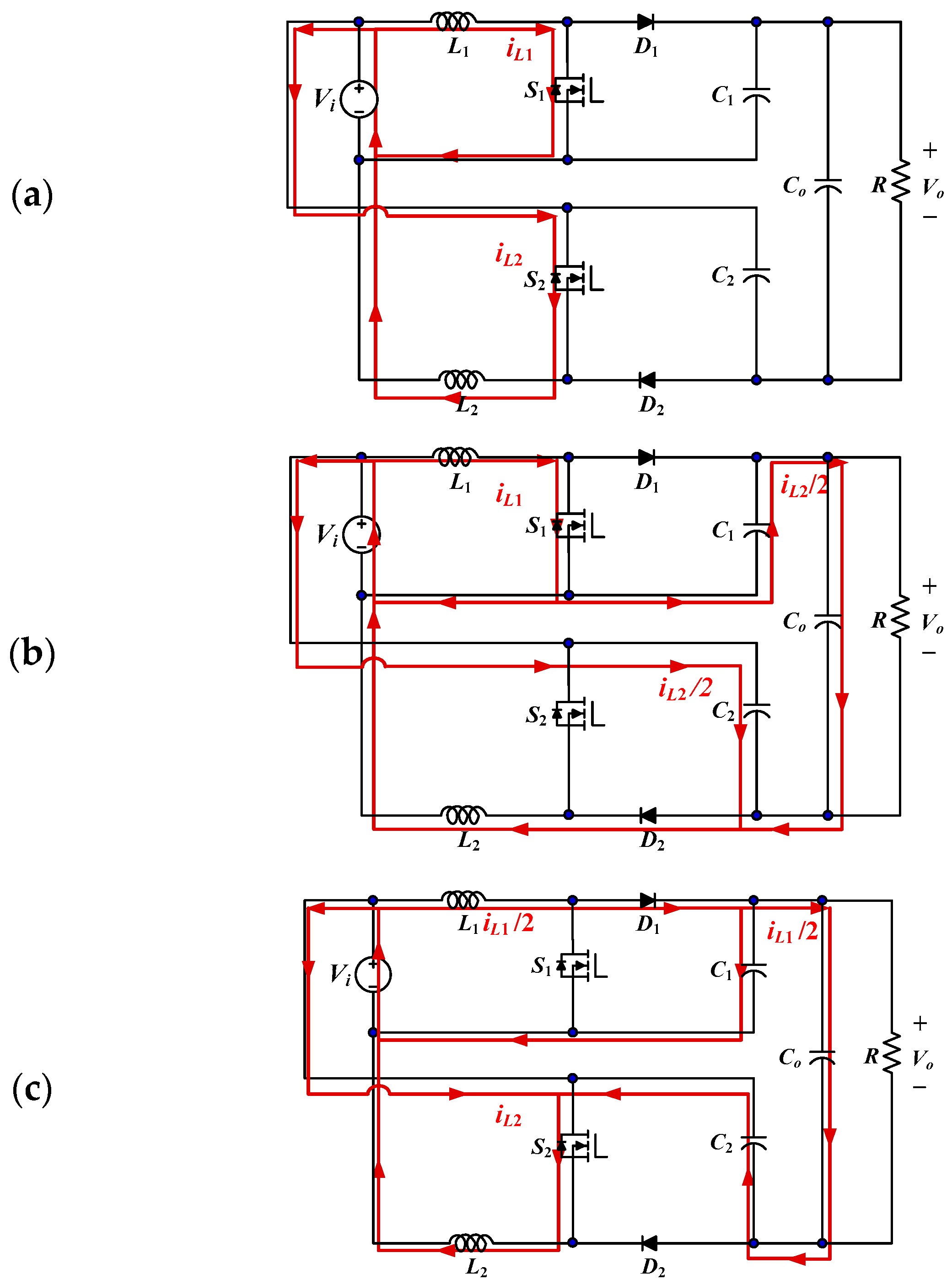
The proposed converter is used as an automotive battery-powered interface. The converter topology for the new combined boost converter contains two-phase circuits, as shown in Figure 2. One is the boost circuit, which involves inductor L1, capacitor C1, active switch S1 and diode D1. The other is the inverted boost circuit, which contains inductor L2, capacitor C2, active switch S2, and diode D2. The inductors L1 and L2 are amount to L, and the capacitors C1 and C2 are amount to C. Co is the common output capacitor, Vi is the supply voltage, Vo is the output voltage, and Ro is the output load resistance.
The following four assumptions are made in analyzing the proposed combined boost converter. (1) For simplicity, it is assumed that all the components in Figure 2 are idealized; (2) All voltages and currents in the circuit are periodic in steady-state conditions; (3) For high boost conversion, the duty cycle of the major switch is exceed 50%, which is presented as D, and the switching period is denoted as Ts; (4) The converter works in continuous conduction mode (CCM). In the combined boost converter, all working modes and their equivalent circuits corresponding to the ON/OFF status of the active switches have been illustrated in Figure 3. The steady-state waveforms of the combined boost converter are demonstrated in Figure 4. The working modes can be described clearly as follows.
- (1)
- Mode 1 [t0–t1] and Mode 3 [t2–t3]: In these two modes, the active switches S1 and S2 are switched on while the diodes, D1 and D2 are reverse-bias. The current in the inductors, iL1 and iL2, increase to store energy in L1 and L2, respectively. The output power for the back-end amplifier is provided by capacitor Co. The total current iLt and inductor currents of L1 and L2 are expressed below.
- (2)
- Mode 2 [t1–t2]: The active switch S1 remains conducting and S2 is switched off. D1 is reverse-bias and D2 is forward-bias. While the current iL1 increase to store energy in L1, the energy stored in inductor L2 is now released through D2, C2, C1, and Co to the output. The total current iLt and inductor currents of L1 and L2 can be expressed as follows:
- (3)
- Mode 4 [t3–t4]: S2 is switched on and S1 is switched off. D2 is reverse-bias and D1 is forward-bias. The energy stored in L1 is released through D1 to charge capacitor C1 and Co. The total current iLt and inductor currents of L1 and L2 can be expressed as follows:
3. Analysis of Steady-State
In this section, the voltage gain, voltage stress on the switches, and inductor current ripple of the combined boost converter working in the steady state are analyzed.
3.1. Voltage Gain
Using Figure 3 and Figure 4, the corresponding state equation for each mode can be obtained. These illustrations enable the observation that the weighting factors in the four working modes which are (D−1/2), (1−D), (D−1/2), and (1−D). The Equations (10) and (11) are obtained using the inductor voltage-second balance principle on L1 and L2 as follows:
The C1 and C2 capacitors are connected in series with the supply voltage, and the equation of output voltage of the converter is expressed as:
By combining (10)–(12), the static voltage gain can be derived by:
The static voltage gain of the conventional boost converter is expressed as:
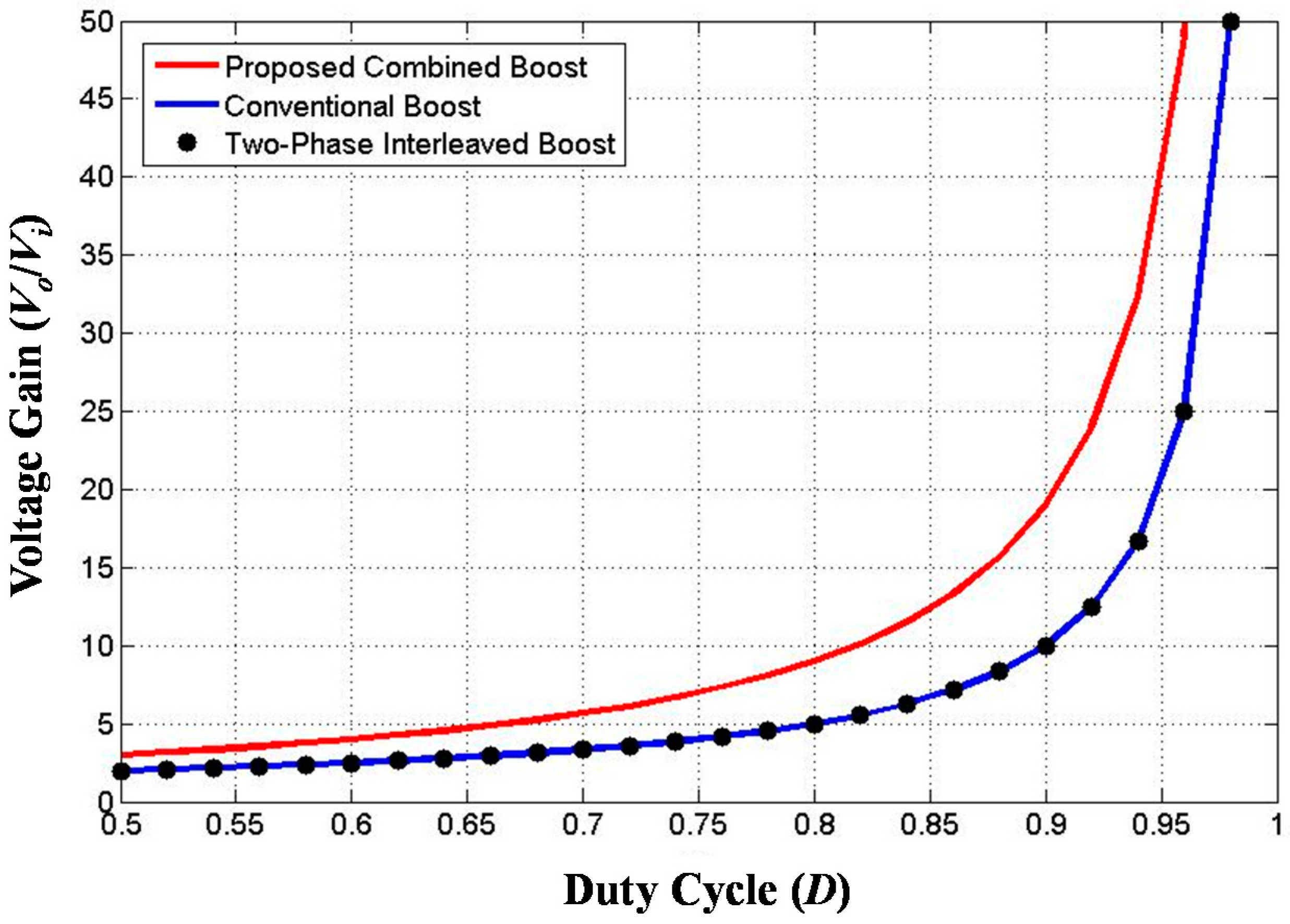
Figure 5 shows a comparison of the voltage gains produced by the proposed combined boost converter, the interleaved boost converter with two-phase and the conventional boost converter. From Figure 5, we observe that the converter has a higher voltage gain than the two-phase interleaved converter and the conventional boost converter.
3.2. Voltage Stress of the Switches
The open circuit voltage stress on switches S1 and S2 can be obtained by the aforementioned analyses of operations. The relevant expression is written as (15).
3.3. Inductor Current Ripples
Using Equations (1)–(9), the total current ripple in the proposed combined boost converter can be represented by:
The current ripples of the inductors L1 and L2, in the proposed combined boost converter can thus be expressed as:
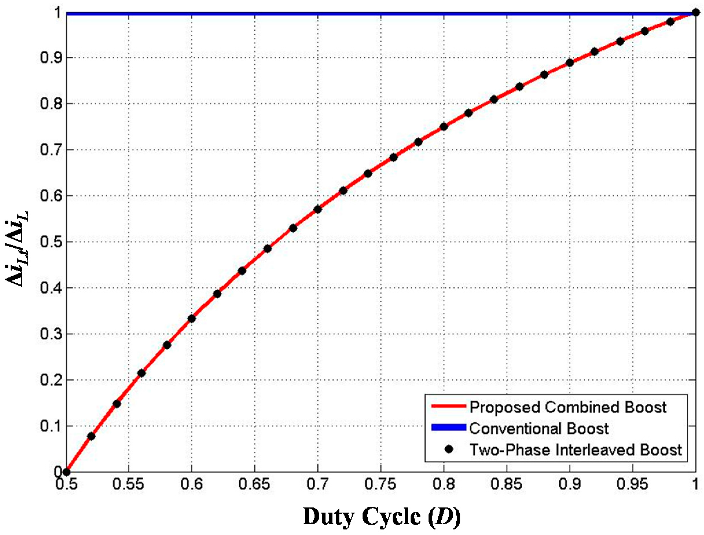
The variation of the duty cycle of the total current ripple to inductor current ripple as a function of the duty cycle is displayed in Figure 6. The proposed converter has the same performance as the two-phase interleaved boost converter, and that is superior to the conventional boost converter.
3.4. The Mode for Boundary Conduction
The boundary normalized inductor time constant τL,B is expressed as:
where fsw is the switching frequency.
The output current during boundary conduction mode (BCM) is indicated by:
Therefore, the boundary normalized time constant is represented by:
Figure 7 shows a plot of the boundary normalized inductor time constant curve. When τL is planned to be higher than the boundary curve of τL,B, the converter operates in continuous conduction mode (CCM). Conversely, the proposed converter works in discontinuous conduction mode (DCM) when τLb is chosen to be smaller than the boundary curve of τLb,B.
3.5. Component Stress and Loss
4. Converter Control Strategy
As described in the preceding paragraphs, the combined boost converter is dominated by the specific duty ratio of switches S1 and S2. By appropriately adjusting duty ratio, the output voltage can be flexible. The circuit model is established by PSIM© simulation software (Powersim Inc., Rockville, MD, USA) under the later suppositions to devise the closed-loop controller and reduce the mathematics for the converter. The suppositions includes (1) power switches and diodes are ideal; (2) equivalent series resistances (ESRs) of all the inductors and capacitors of the converter are thought to acquire a comparatively precise dynamic model; (3) the converter works in under CCM. The taken circuit parameters are L1 = L2 = 250 μH, C1 = C2 = 10 μF, Co = 1000 μF, output resistance R = 30 Ω, and ESRs rL1 = rL2 = rC1 = rC2 = 100 mΩ.
Figure 8 illustrates the block diagram of the combined boost converter by measuring the output voltage feedback signal into the controller for control. Figure 8 illustrates the developed control system for the combined boost converter. It can be seen that the output voltage (Vo) is sensed and compared with the reference (Vo,ref). The output voltage controller produces those two inductor current reference (iL1,ref, iL2,ref) for the entire system, and the equal current sharing between the two interleaved phases can be also acquired. Furthermore, during the system startup, using a soft start system (Vconss) is used to avoid the capacitor charge surge current causing damage to the converter components.
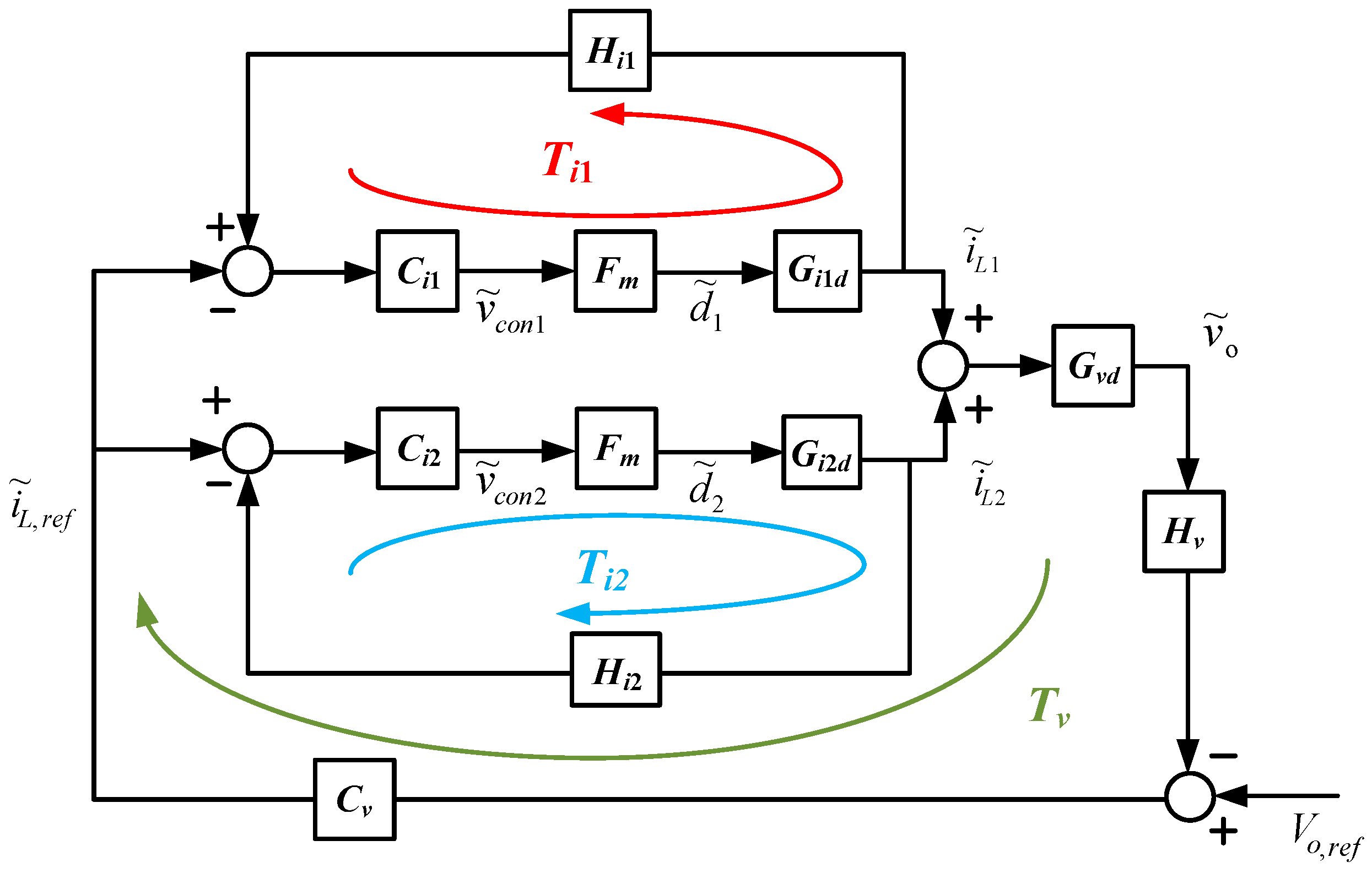
The Block diagram of the closed-loop control scheme is shown in Figure 9. In the inner current control loop, FM is the constant gain of the PWM generator; Gi1d and Gi2d is the transfer function from the duty ratio to the two different inductor current; Ci1 and Ci2 indicates the transfer function of current controllers; and Hi1 and Hi2 are the sensing gains of the current sensor. In the outer voltage control loop, Gvd is the transfer function from the duty ratio to the output voltage; Cv indicates the transfer function of output voltage controller; and Hv indicates the sensing gain of the voltage sensor.
From Figure 9, we can derive open the loop gain of the voltage and current loops of the proposed converter by the following equations.
where, FM = 1/100, Hi1 = Hi2 = Hv = 1.
The small-signal transfer from the duty ratio to those inductor current Gi1d and Gi2d and the duty ratio to output voltage Gvd can be shown below.
A uncomplicated type-II controller that comprise one-zero, one-pole, and another one-pole at the origin is employed for the current loop compensation to offer sufficient DC gain, bandwidth, gain/phase margins for the system. In addition, a proportional-integral (PI) controller that contain one-zero and one-pole at origin is applied for the voltage loop compensation.
The corresponding current/voltage controllers of the converter are selected as follows:
Figure 10a shows the frequency response of the loop gain for compensated current loop, under the full-load conditions. This work leads to a phase margin of 55 degrees and the crossover frequency is approximately 8 kHz.
Figure 10b shows the frequency response of the loop gain for compensated voltage loop, under the full-load conditions. This work leads to a phase margin of 45 degrees and the crossover frequency is approximately 800 Hz.
5. Simulated and Experimented Results
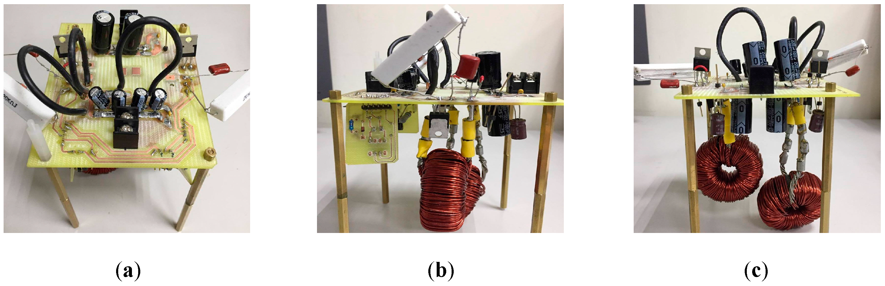
In order to confirm the performance of the combined boost converter, simulations and experiments were conducted based on the test setup shown in Figure 11. Figure 12 shows a three-view photograph of the realized boost converter prototype. Figure 13 shows the realized test bench, which consists of an oscilloscope, a power source, an electronics load, a PWM generator, and the proposed combined boost converter prototype.
The specifications and parameters of the components taken in the converter prototype are provided in Table 3 and Table 4, respectively.
For input voltage of 12V and duty cycle of 66.7%, output voltage of 60 V can be obtained using (13). The voltages on the capacitors of C1 and C2 are calculated using (10) and (11). The values across both C1 and C2 are calculated to be about 36 V (i.e., VC1 = VC2 = 36 V).
PSIM© simulation software (Powersim Inc., Rockville, MD, USA) is used to confirm the feasibility of the combined boost converter. Figure 14 and Figure 15 indicate the simulated and experimented waveforms of the combined boost converter for gate driving signals VGS1 and VGS2 and two-phase inductor currents iL1 and iL2, respectively.
Figure 16 shows the simulated and experimented waveforms of the combined boost converter for the cross voltages across S1 and S2, respectively.
Figure 17 shows the simulated and experimented waveforms of the combined boost converter for the cross voltages across D1 and D2, respectively.
Figure 18 shows the simulated and experimented waveforms of the combined boost converter for the voltages across the C1 and C2 capacitors. The results verify the feasibility of the converter.
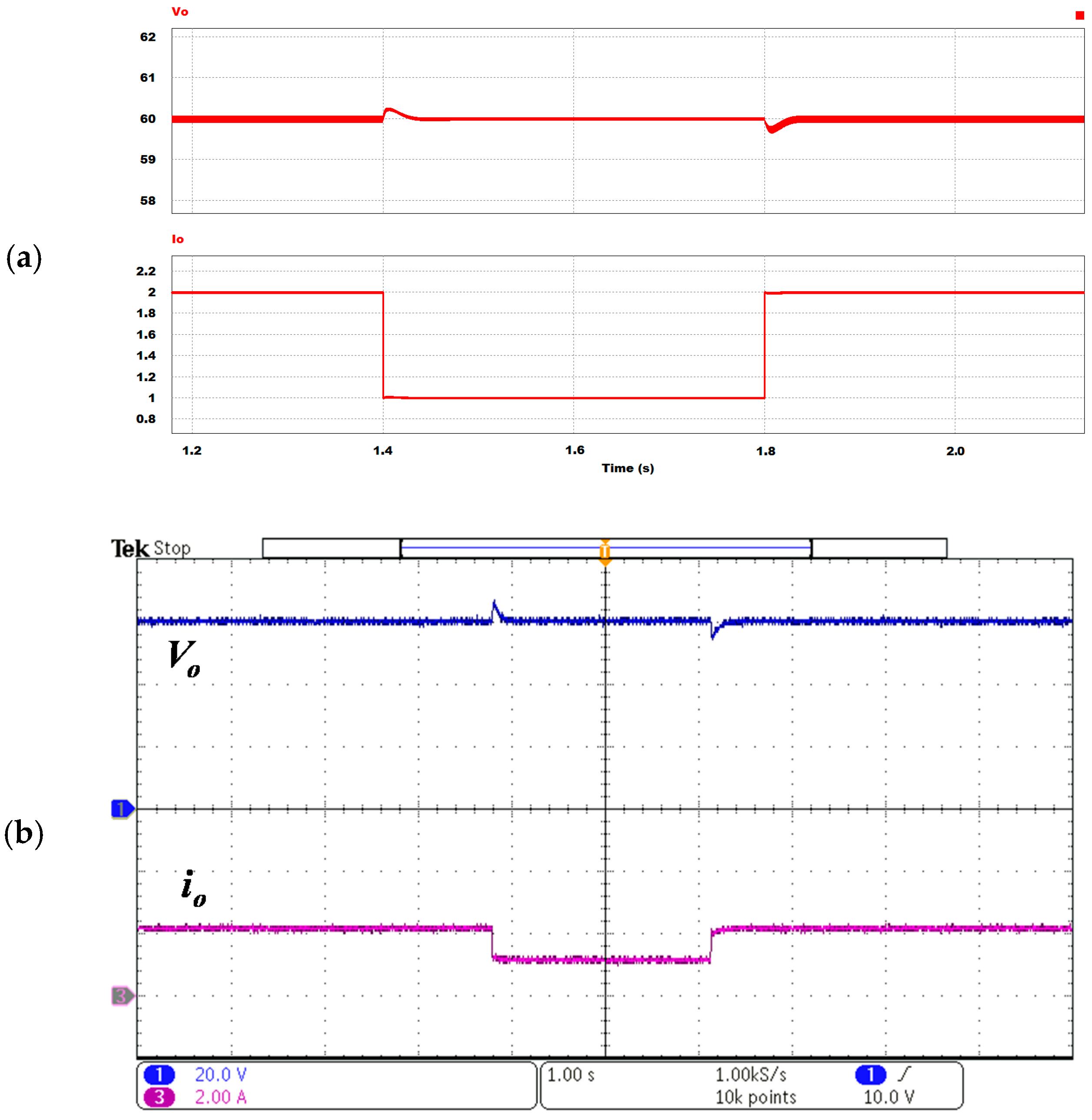
Figure 19 shows the transient response because of a step load current change between 120 W and 60 W for the combined boost converter prototype. As can be seen from Figure 19, the output voltage can be stably regulated to be 60 V under the load current variation between 1 A and 2 A.
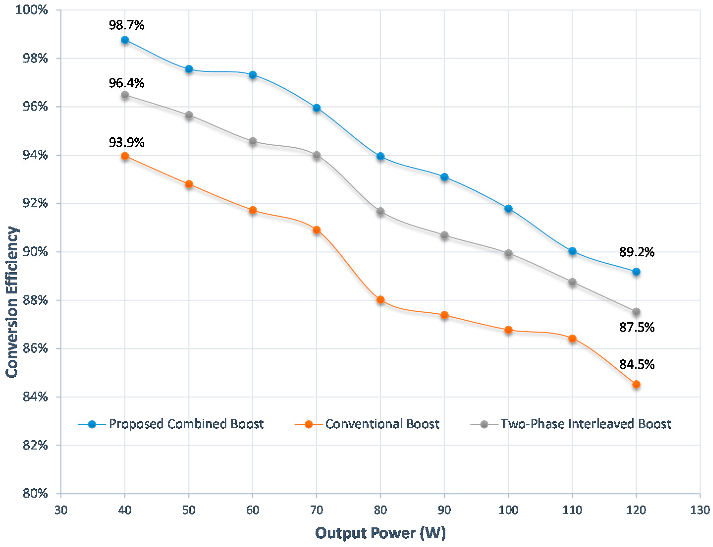
Figure 20 shows the measured conversion efficiency of the combined boost converter, the interleaved boost converter with a two-phases and the conventional converter. The conversion efficiency is measured via precise digital power meter equipment, Yokogawa WT310 (Yokogawa Electric Corporation, Tokyo, Japan). Using the proposed combined boost converter, we obtain the maximum conversion efficiency is 98.7%, as well as the conversion efficiency with a full load is 89.2%. The proposed combined boost converter owns higher efficiency under full load conditions because the conduction loss can be cut down through applying the low-voltage-rated devices.
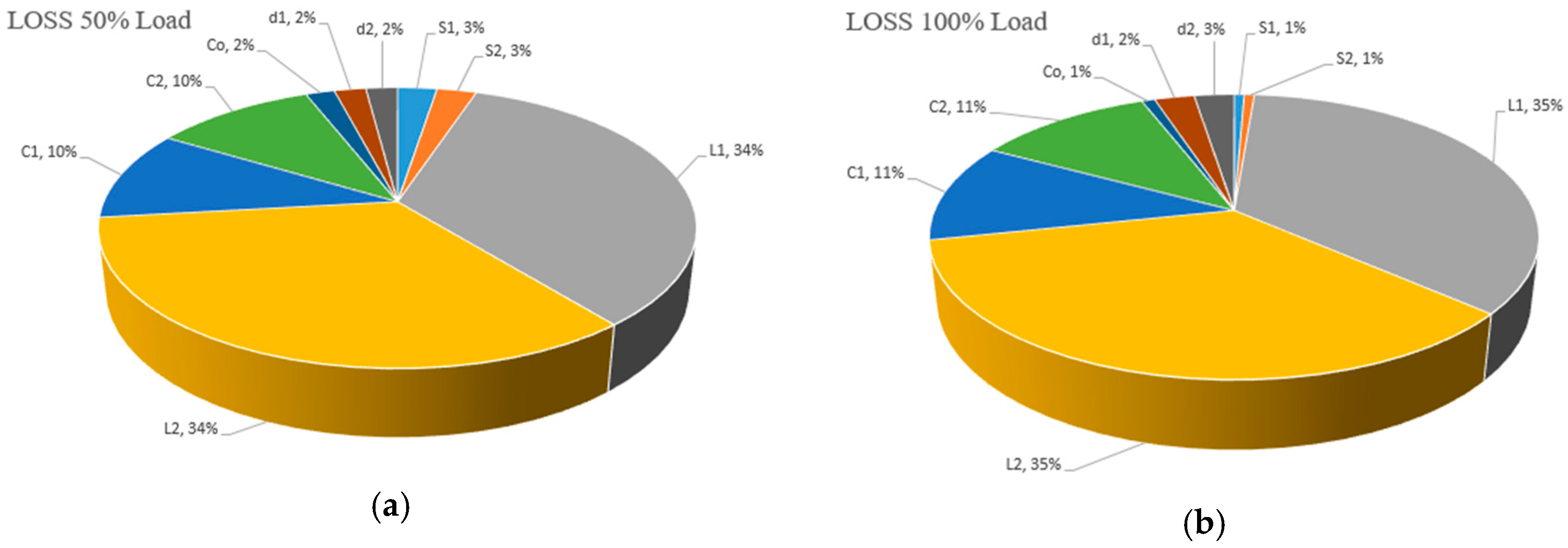
The calculated interleaved boost converter power loss distribution at the rated load condition, obtained using the equations in Table 2, is listed in Table 5 to expound the measured conversion efficiency. Furthermore, the resulting loss breakdown charts are depicted in Figure 21.
For the sake of verifying the performance of the proposed combined boost converter, the other three converters published in [11,19,24] are used for comparison here, as shown in Table 6. It can be observed that the amounts of passive components in [19] exceed the requirement in the converter. It will lead to an increase in manufacturing costs.
The voltage gain of the former converter [11] is equal to the proposed one presented in this work, Although the former converter in [11] has the relatively low-cost components, the input current ripple is large because of the active switches being controlled simultaneously by using one control signal. The voltage gain of the previous converter in [24] is slightly larger than that of the proposed converter in this study; however, the input current ripple is large owing to the single-phase operation makes this converter not suitable for high current and low ripple applications.
From the point view of the cost–performance ratio, the proposed combined boost converter really carries out the higher conversion efficiency and also lower input current ripple under 120 W power rating than other existing works [11,19,24]. Based on its features, this converter can be as a suitable candidate for 12 V battery-powered front-end stage for supplying an automotive audio amplifier.
6. Conclusions
A modified interleaved boost converter with two-phase is presented as a battery-powered front-end interface for automotive audio amplifiers. The combined boost converter is created based on a two-phase structure by combining the conventional boost converter with its inverted type. As well as the existing characteristics that benefit from interleaved converters, the converter provides the more advantages in extending the duty cycle than the conventional boost and the interleaved boost converters. Furthermore, it also prevents working with a wide duty cycle. The operating principles, steady-state analyzes, as well as the closed-loop control designs of the converter are explored in this study.
Simulations and experiments are also performed using input voltage of 12 V for a 120 W circuit. A reasonable duty cycle of 0.67 is selected to reach output voltage of 60 V, which corresponds to static voltage gain of five. The converter achieves a maximum measured conversion efficiency of 98.7%. According to its characteristics, the combined boost converter is highly suitable for use as a front-end converter in powering automotive audio amplifiers.
Acknowledgments
This work is partly supported by the Ministry of Science and Technology (MOST) in Taiwan under grants MOST 105-2221-E-027-096, MOST 105-2221-E-324-02, MOST 105-2221-E-324-026, and MOST 106-2218-E-027-010. The authors would like to express their appreciation to the student Chao-Wei Ku (NTUT) for the experimental bench setup.
Author Contributions
Ching-Ming Lai substantially contributed to examination and interpretation of the results, development of the overall system, and review and proofreading of the manuscript. Yu-Huei Cheng substantially contributed to control strategy design, production and analysis of the results, and preparation and revision of the manuscript. Jiashen Teh substantially contributed to the review and proofreading of the manuscript. Yuan-Chih Lin substantially contributed to literature search, control strategy design, and production and analysis of the results.
Conflicts of Interest
The authors declare no conflict of interest.
References
- Kim, C.-E.; Moon, G.-W. High-efficiency low-profile on-board DC/DC converter for digital car audio amplifier. Electron. Lett. 2004, 40, 571–572. [Google Scholar] [CrossRef]
- Kim, C.-E.; Han, S.-K.; Moon, G.-W. A New High Efficiency and Low Profile On-Board DC/DC Converter for Digital Car Audio Amplifiers. J. Power Electron. 2006, 6, 83–93. [Google Scholar]
- Kim, C.-E.; Moon, G.-W.; Han, S.-K. Voltage doubler rectified boost-integrated half bridge (VDRBHB) converter for digital car audio amplifiers. IEEE Trans. Power Electron. 2007, 22, 2321–2330. [Google Scholar] [CrossRef]
- Lee, B.-H.; Kim, C.-E.; Moon, G.-W. A New Non-isolated ZVZCS Voltage Doubler Rectified Boost-integrated Half-Bridge (VDRBIHB) DC/DC Converter for Digital Car Audio Amplifier Power Supply. In Proceedings of the Power Electronics Specialists Conference, Orlando, FL, USA, 17–21 June 2007; pp. 331–336. [Google Scholar]
- Franceschini, G.; Lorenzani, E.; Cavatorta, M.; Bellini, A. 3boost: A high-power three-phase step-up full-bridge converter for automotive applications. IEEE Trans. Ind. Electron. 2008, 55, 173–183. [Google Scholar] [CrossRef]
- Berkhout, M.; Dooper, L.; Krabbenborg, B. A 4 Ω 2.65 W Class-D Audio Amplifier With Embedded DC–DC Boost Converter, Current Sensing ADC and DSP for Adaptive Speaker Protection. IEEE J. Solid-State Circuits 2013, 48, 2952–2961. [Google Scholar] [CrossRef]
- Lai, C.-M.; Lee, Y.-H.; Lin, Y.-C.; Ku, C.-W. Study and Analysis of a Battery-Powered High Step-Up Front-End Converter for Automotive Audio Amplifier. In Proceedings of the 2016 IEEE Vehicle Power and Propulsion Conference (VPPC), Hangzhou, China, 17–20 October 2016; pp. 1–4. [Google Scholar]
- Reatti, A. Low-cost high power-density electronic ballast for automotive HID lamp. IEEE Trans. Power Electron. 2000, 15, 361–368. [Google Scholar] [CrossRef]
- Zhao, Q.; Hu, Y.; Lee, F.C.; Sabate, J.A.; Li, F. A high efficiency DC/DC converter as the front-end stage of high intensity discharge lamp ballasts for automobiles. In Proceedings of the Third International Power Electronics and Motion Control Conference, Beijing, China, 15–18 August 2000; pp. 752–756. [Google Scholar]
- Zhao, Q.; Lee, F.C. High-efficiency, high step-up DC–DC converters. IEEE Trans. Power Electron. 2003, 18, 65–73. [Google Scholar] [CrossRef]
- Yang, L.S.; Liang, T.J.; Chen, J.F. Transformerless DC–DC converters with high step-up voltage gain. IEEE Trans. Power Electron. 2009, 56, 3144–3152. [Google Scholar] [CrossRef]
- Divakar, B.; Cheng, K.W.E.; Wang, D.; Ping, D.; Kwok, K. Implementation of a voltage multiplier integrated HID ballast circuit with dimming control for automotive application. IEEE Trans. Power Electron. 2009, 56, 2479–2492. [Google Scholar] [CrossRef]
- Tomm, F.L.; Seidel, Á.R.; Campos, A.; Dalla Costa, M.A.; do Prado, R.N. HID lamp electronic ballast based on chopper converters. IEEE Trans. Power Electron. 2012, 59, 1799–1807. [Google Scholar] [CrossRef]
- Babu, T.; Balakrishnan, A.A. Quadrupler DC converter for high intensity discharge lamp applications, Circuit. In Proceedings of the 2015 International Conference on Circuit, Power and Computing Technologies (ICCPCT), Nagercoil, India, 19–20 March 2015; pp. 1–6. [Google Scholar]
- Silva, C.E.; Bascope, R.P.; Oliveira, D.S. Proposal of a new high step-up converter for UPS applications. In Proceedings of the 2006 IEEE International Symposium on Industrial Electronics, Montreal, QC, Canada, 9–13 July 2006; pp. 1288–1292. [Google Scholar]
- Da Câmara, R.A.; Cruz, C.M.; Torrico-Bascopé, R.P. Boost based on three-state switching cell for UPS applications. In Proceedings of the 2009 Brazilian Power Electronics Conference, Bonito-Mato Grosso do Sul, Brazil, 27 September–1 October 2009; pp. 313–318. [Google Scholar]
- Araújo, S.V.; Torrico-Bascopé, R.P.; Torrico-Bascopé, G.V. Highly efficient high step-up converter for fuel-cell power processing based on three-state commutation cell. IEEE Trans. Power Electron. 2010, 57, 1987–1997. [Google Scholar] [CrossRef]
- Lelie, M.; Rothgang, S.; Masomtob, M.; Rosekeit, M.; Doncker, R.W.D.; Sauer, D.U. Design of a Battery System for a Fuel Cell Powered UPS ApplicationWith Extreme Temperature Conditions. In Proceedings of the 2013 35th International Telecommunications Energy Conference ‘Smart Power and Efficiency’ (INTELEC), Hamburg, Germany, 13–17 October 2013. [Google Scholar]
- Lai, C.-M. A battery-powered single-stage three-phase high step-up converter topology for micro DC-UPS. IEICE Electron. Express 2014, 11, 20140852. [Google Scholar] [CrossRef]
- Emadi, A.; Rajashekara, K.; Williamson, S.S.; Lukic, S.M. Topological overview of hybrid electric and fuel cell vehicular power system architectures and configurations. IEEE Trans. Veh. Technol. 2005, 54, 763–770. [Google Scholar] [CrossRef]
- Camara, M.B.; Gualous, H.; Gustin, F.; Berthon, A. Design and new control of DC/DC converters to share energy between supercapacitors and batteries in hybrid vehicles. IEEE Trans. Veh. Technol. 2008, 57, 2721–2735. [Google Scholar] [CrossRef]
- Khaligh, A.; Li, Z. Battery, ultracapacitor, fuel cell, and hybrid energy storage systems for electric, hybrid electric, fuel cell, and plug-in hybrid electric vehicles: State of the art. IEEE Trans. Veh. Technol. 2010, 59, 2806–2814. [Google Scholar] [CrossRef]
- Shahin, A.; Hinaje, M.; Martin, J.; Pierfederici, S.; Rae, X.; Rael, S.L.; Davat, B. High voltage ratio DC–DC converter for fuel-cell applications. IEEE Trans. Power Electron. 2010, 57, 3944–3955. [Google Scholar] [CrossRef]
- Ardi, H.; Ahrabi, R.R.; Ravadanegh, S.N. Non-isolated bidirectional DC–DC converter analysis and implementation. IET Power Electron. 2014, 7, 3033–3044. [Google Scholar] [CrossRef]
- Thounthong, P. Control of a three-level boost converter based on a differential flatness approach for fuel cell vehicle applications. IEEE Trans. Veh. Technol. 2012, 61, 1467–1472. [Google Scholar] [CrossRef]
- Yang, L.-S.; Liang, T.-J. Analysis and implementation of a novel bidirectional DC–DC converter. IEEE Trans. Power Electron. 2012, 59, 422–434. [Google Scholar] [CrossRef]
- Pavlovsky, M.; Guidi, G.; Kawamura, A. Assessment of coupled and independent phase designs of interleaved multiphase buck/boost DC–DC converter for EV power train. IEEE Trans. Power Electron. 2014, 29, 2693–2704. [Google Scholar] [CrossRef]
- Lai, C.-M.; Lin, Y.-C.; Lee, D. Study and implementation of a two-phase interleaved bidirectional DC/DC converter for vehicle and dc-microgrid systems. Energies 2015, 8, 9969–9991. [Google Scholar] [CrossRef]
- Lai, C.-M. Development of a novel bidirectional DC/DC converter topology with high voltage conversion ratio for electric vehicles and DC-microgrids. Energies 2016, 9, 410. [Google Scholar] [CrossRef]
- Lin, Y.-S.; Hu, K.-W.; Yeh, T.-H.; Liaw, C.-M. An electric-vehicle IPMSM drive with interleaved front-end DC/DC converter. IEEE Trans. Veh. Technol. 2016, 65, 4493–4504. [Google Scholar] [CrossRef]
- Lai, C.-M.; Pan, C.-T.; Cheng, M.-C. High-efficiency modular high step-up interleaved boost converter for DC-microgrid applications. IEEE Trans. Ind. Appl. 2012, 48, 161–171. [Google Scholar] [CrossRef]
- Mohr, M.; Franke, W.; Wittig, B.; Fuchs, F. Converter systems for fuel cells in the medium power range—A comparative study. IEEE Trans. Power Electron. 2010, 57, 2024–2032. [Google Scholar] [CrossRef]
- Li, W.; He, X. Review of nonisolated high-step-up DC/DC converters in photovoltaic grid-connected applications. IEEE Trans. Power Electron. 2011, 58, 1239–1250. [Google Scholar] [CrossRef]
- AN-9010 MOSFET Basics. Available online: https://www.fairchildsemi.com/application-notes/AN/AN-9010.pdf (accessed on 27 July 2017).
- STPS8H100 Spec. Available online: http://www.st.com/en/diodes-and-rectifiers/stps8h100.html (accessed on 5 June 2017).
Figure 1.
Illustration of the studied audio amplifier architecture.
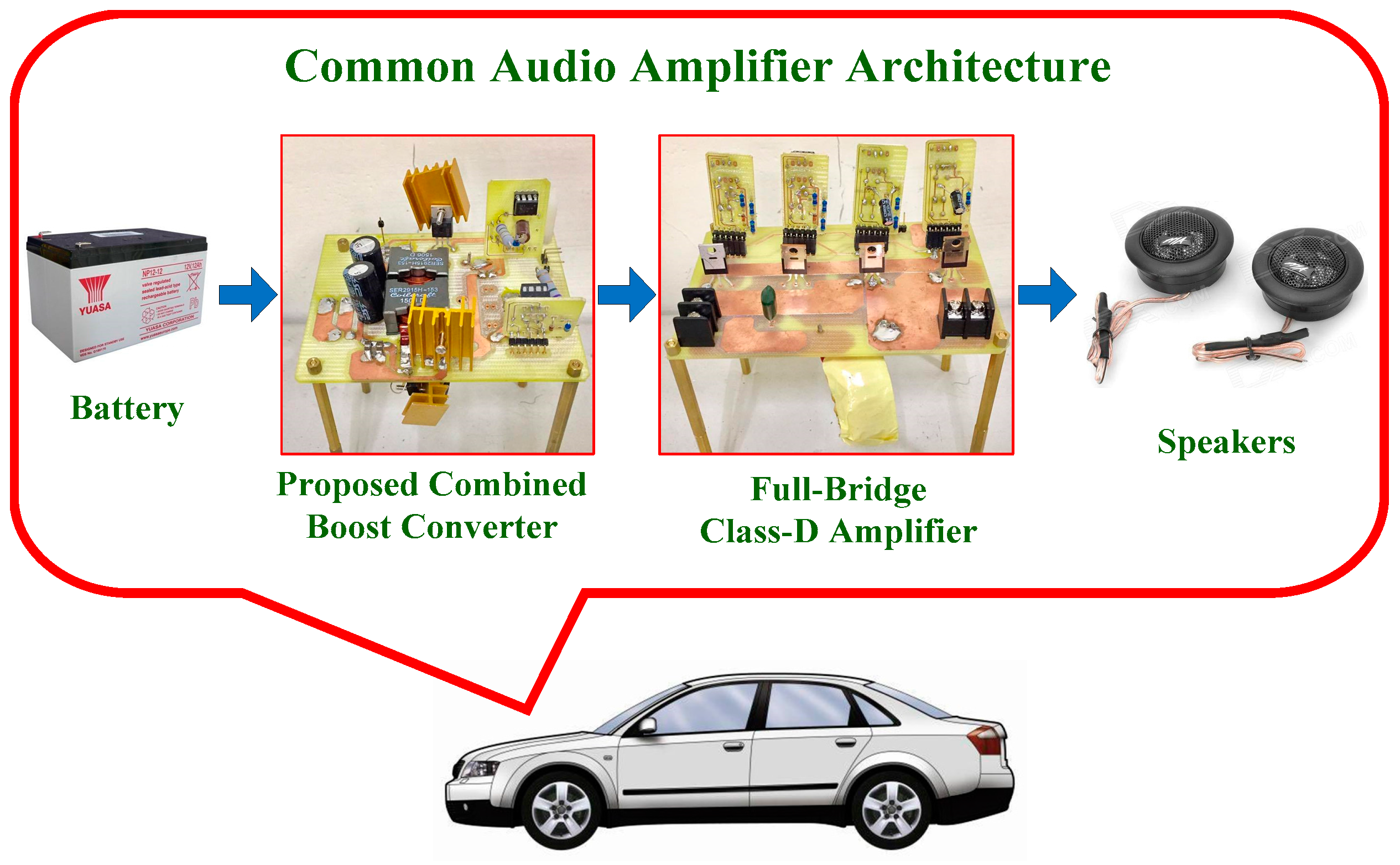
Figure 2.
Proposed combined boost converter topology.

Figure 3.
Working modes and equivalent circuits of the combined boost converter. (a) Mode 1 and Mode 3, (b) Mode 2, and (c) Mode 4.
Figure 3.
Working modes and equivalent circuits of the combined boost converter. (a) Mode 1 and Mode 3, (b) Mode 2, and (c) Mode 4.

Figure 4.
Depicted steady-state waveforms of the combined boost converter.
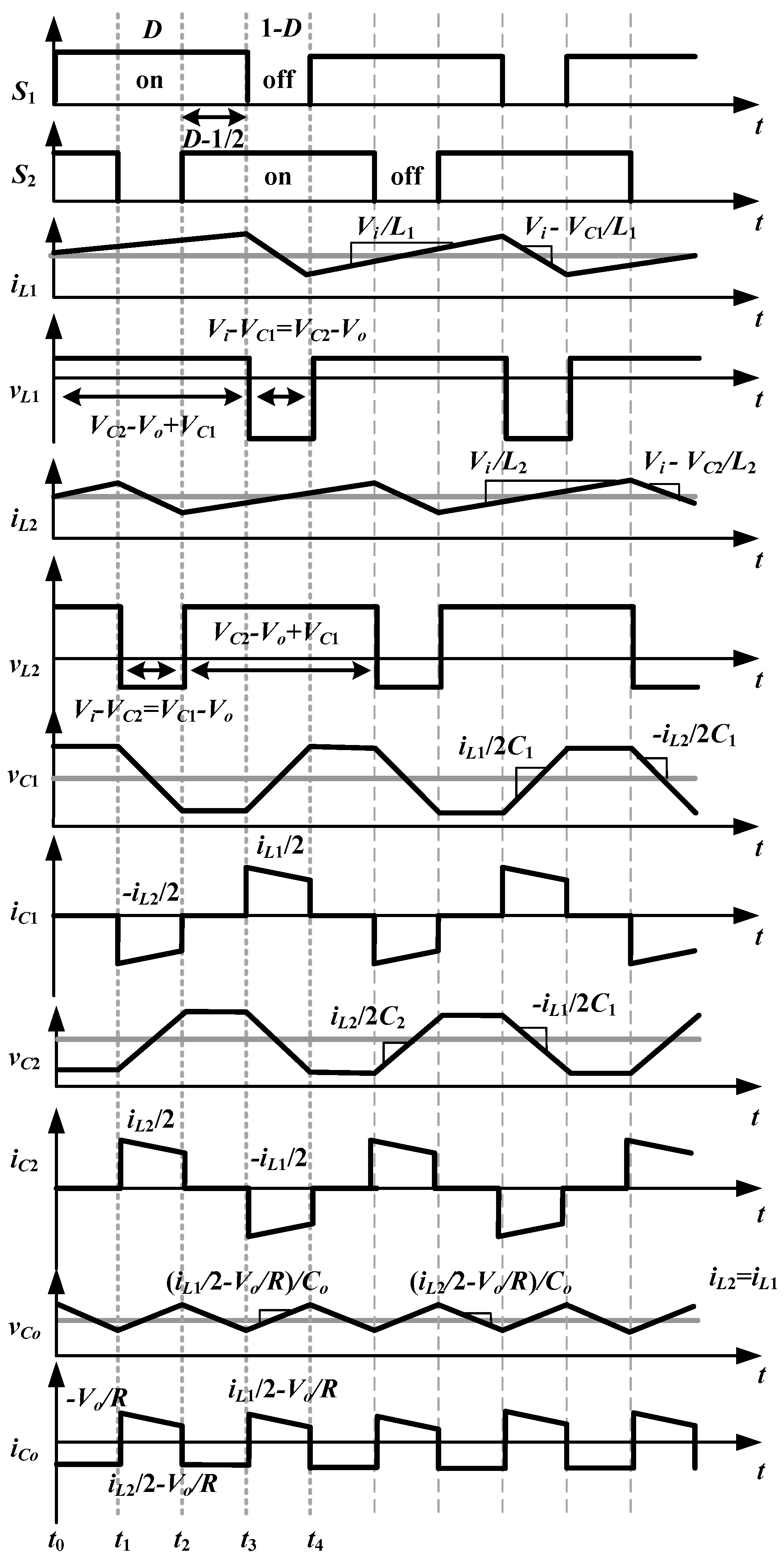
Figure 5.
The comparison of the voltage gains produced by the proposed combined boost converter, the conventional boost converter, and the interleaved boost converter with two-phases.
Figure 5.
The comparison of the voltage gains produced by the proposed combined boost converter, the conventional boost converter, and the interleaved boost converter with two-phases.

Figure 6.
The ratio between the total current ripple and the inductor current ripple versus the duty cycle.
Figure 6.
The ratio between the total current ripple and the inductor current ripple versus the duty cycle.

Figure 7.
Normalized boundary inductance-time constant curve.
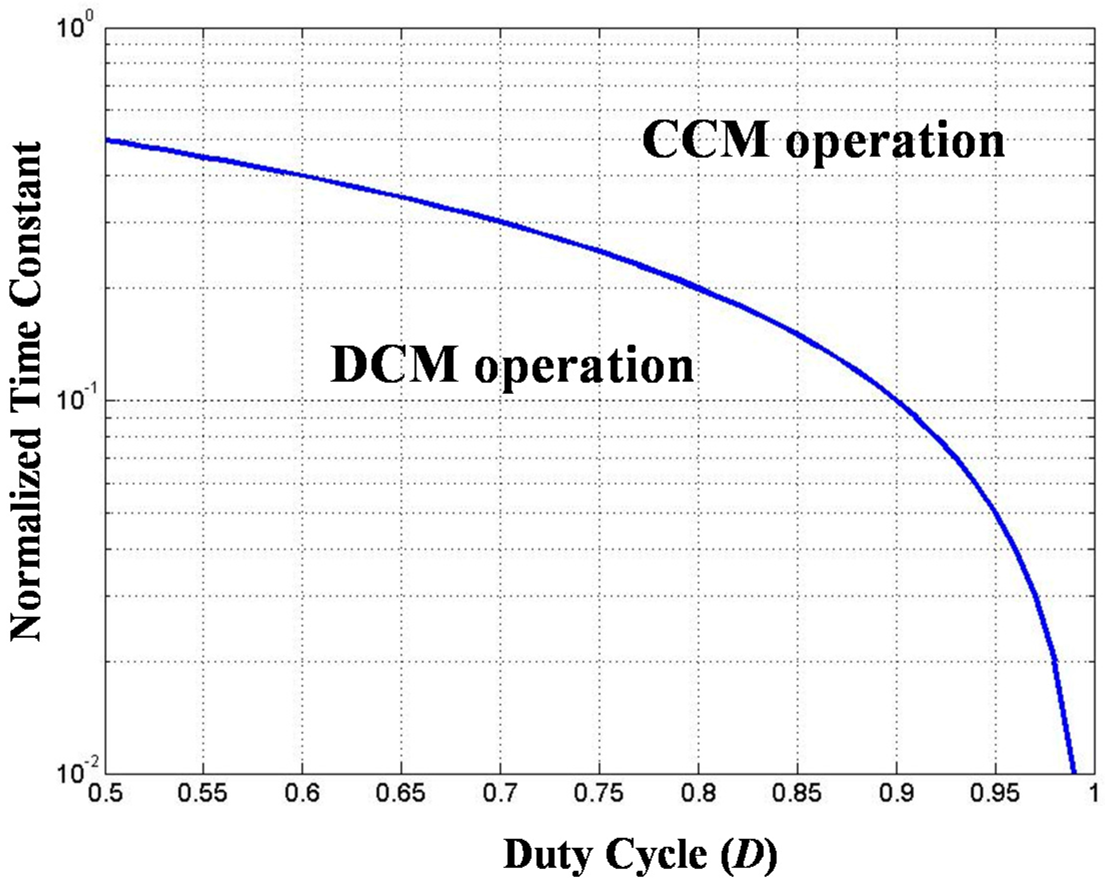
Figure 8.
The developed control system for the combined boost converter.
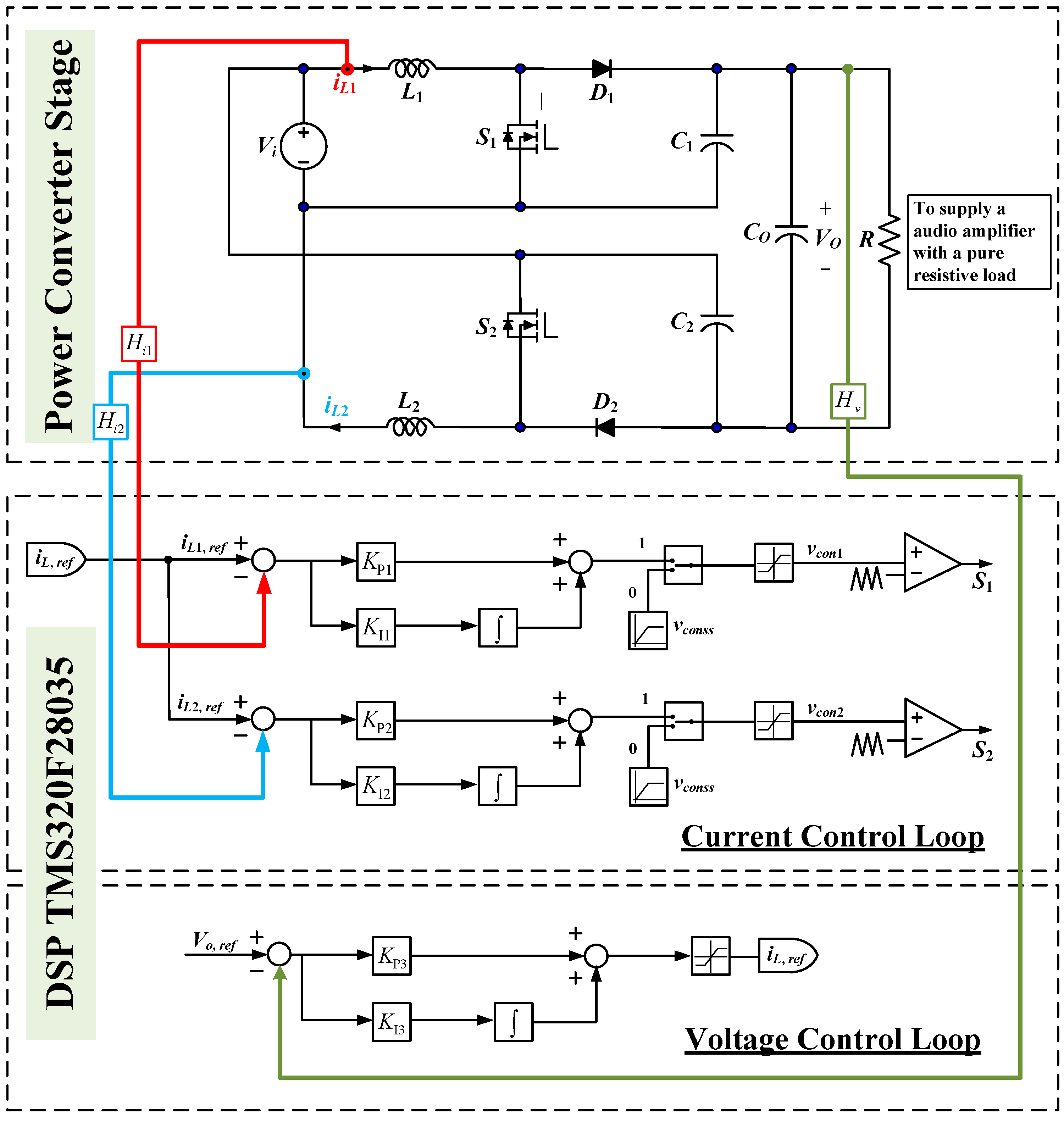
Figure 9.
Block diagram for the closed-loop control scheme.

Figure 10.
Frequency responses of the loop gain. (a) compensated current loop and (b) compensated voltage loop.
Figure 10.
Frequency responses of the loop gain. (a) compensated current loop and (b) compensated voltage loop.
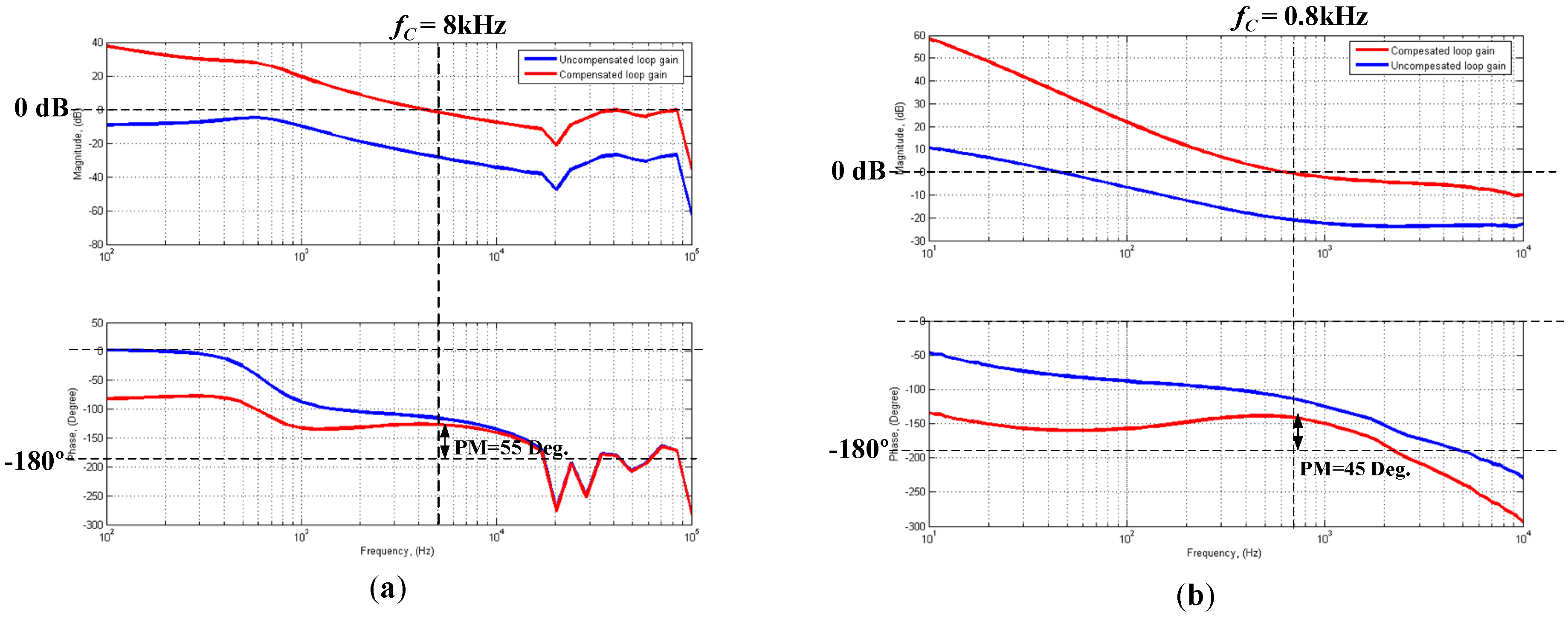
Figure 11.
Block diagram of the experimental test setup.
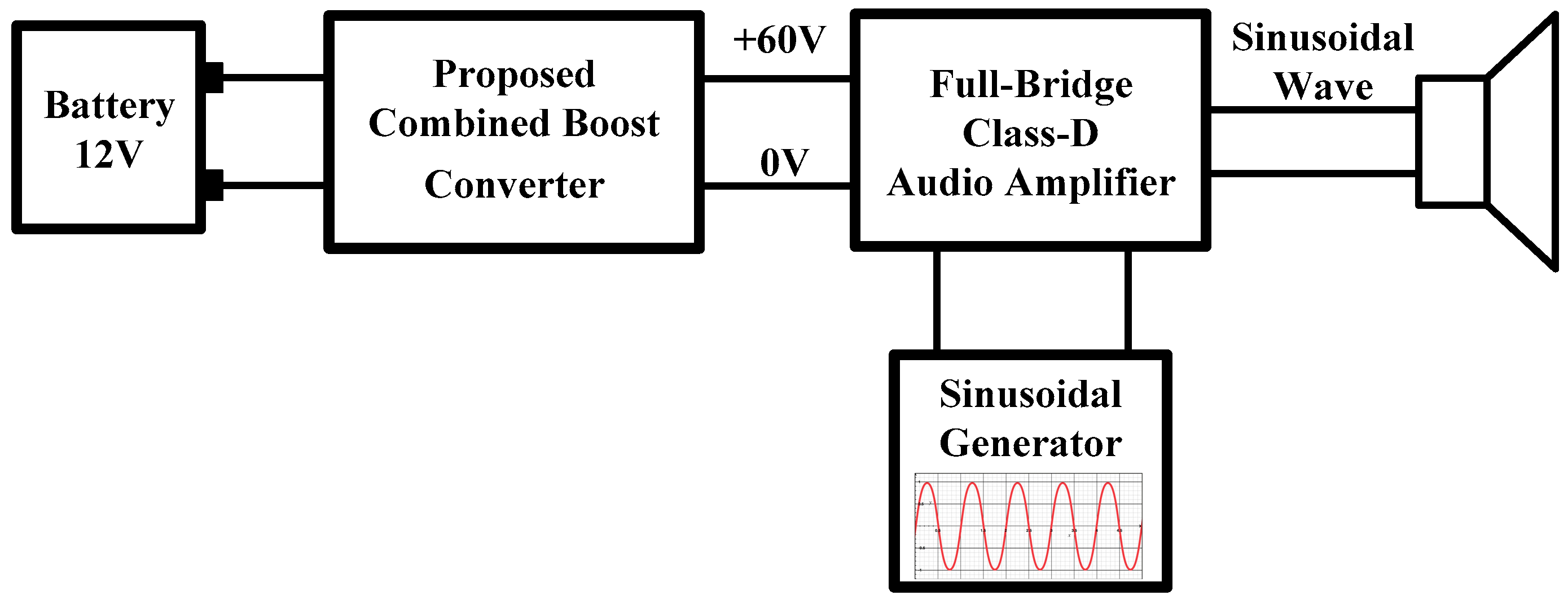
Figure 12.
Realized combined boost converter prototype. (a) Top view; (b) Front view; (c) Side view.
Figure 12.
Realized combined boost converter prototype. (a) Top view; (b) Front view; (c) Side view.

Figure 13.
Realized test bench system (the oscilloscope, power source, electronics load, pulse-width modulation (PWM) generator, and the proposed combined boost converter prototype are labeled).
Figure 13.
Realized test bench system (the oscilloscope, power source, electronics load, pulse-width modulation (PWM) generator, and the proposed combined boost converter prototype are labeled).
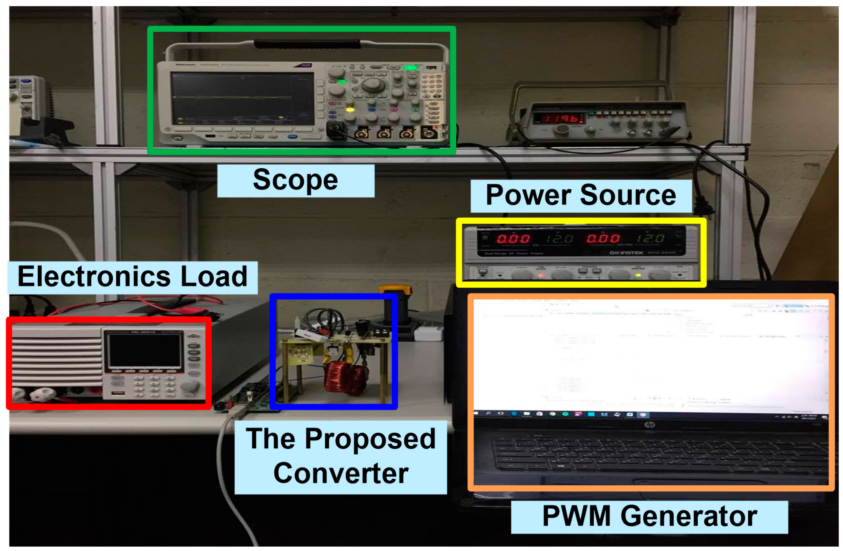
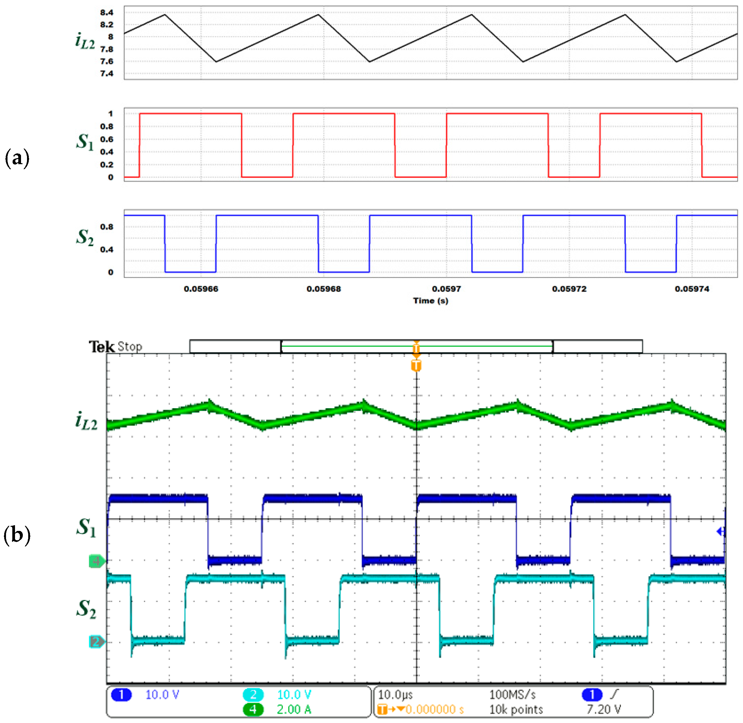
Figure 14.
Waveforms of the combined boost converter for gate driving signals Vgs1 and Vgs2 and two-phase inductor current iL1. (a) Simulated waveforms; (b) Experimented waveforms.
Figure 14.
Waveforms of the combined boost converter for gate driving signals Vgs1 and Vgs2 and two-phase inductor current iL1. (a) Simulated waveforms; (b) Experimented waveforms.
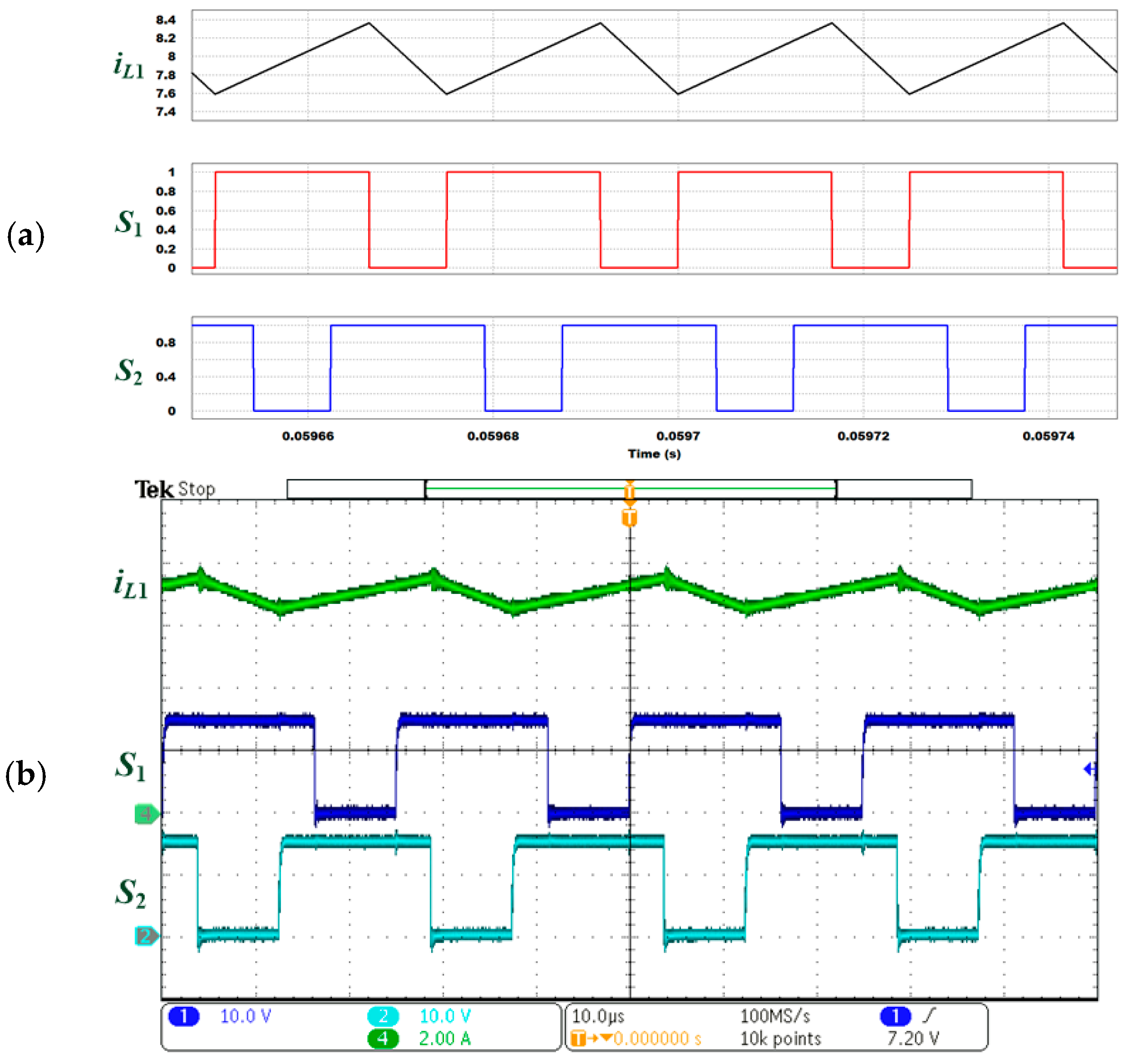
Figure 15.
Waveforms of the combined boost converter for gate driving signals VGS1 and VGS2 and two-phase inductor current iL2. (a) Simulated waveforms; (b) Experimented waveforms.
Figure 15.
Waveforms of the combined boost converter for gate driving signals VGS1 and VGS2 and two-phase inductor current iL2. (a) Simulated waveforms; (b) Experimented waveforms.

Figure 16.
Waveforms of the combined boost converter for the cross voltages across S1 and S2. (a) Simulated waveforms; (b) Experimented waveforms.
Figure 16.
Waveforms of the combined boost converter for the cross voltages across S1 and S2. (a) Simulated waveforms; (b) Experimented waveforms.
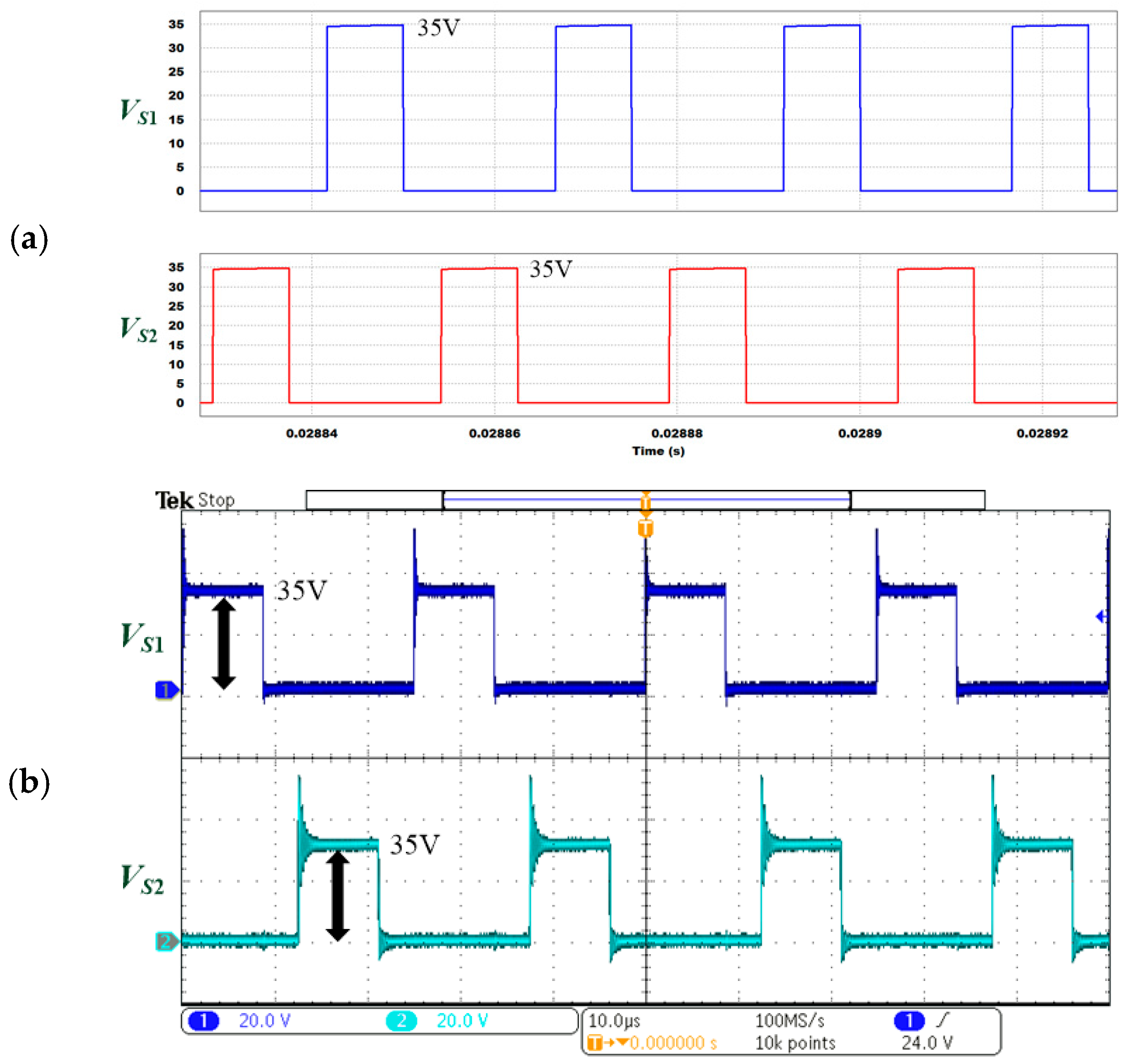
Figure 17.
Waveforms of the proposed combined boost converter for the cross voltages across D1 and D2. (a) Simulated waveforms; (b) Experimented waveforms.
Figure 17.
Waveforms of the proposed combined boost converter for the cross voltages across D1 and D2. (a) Simulated waveforms; (b) Experimented waveforms.

Figure 18.
Waveforms of the combined boost converter for the cross voltages across C1 and C2. (a) Simulated waveforms; (b) Experimented waveforms.
Figure 18.
Waveforms of the combined boost converter for the cross voltages across C1 and C2. (a) Simulated waveforms; (b) Experimented waveforms.
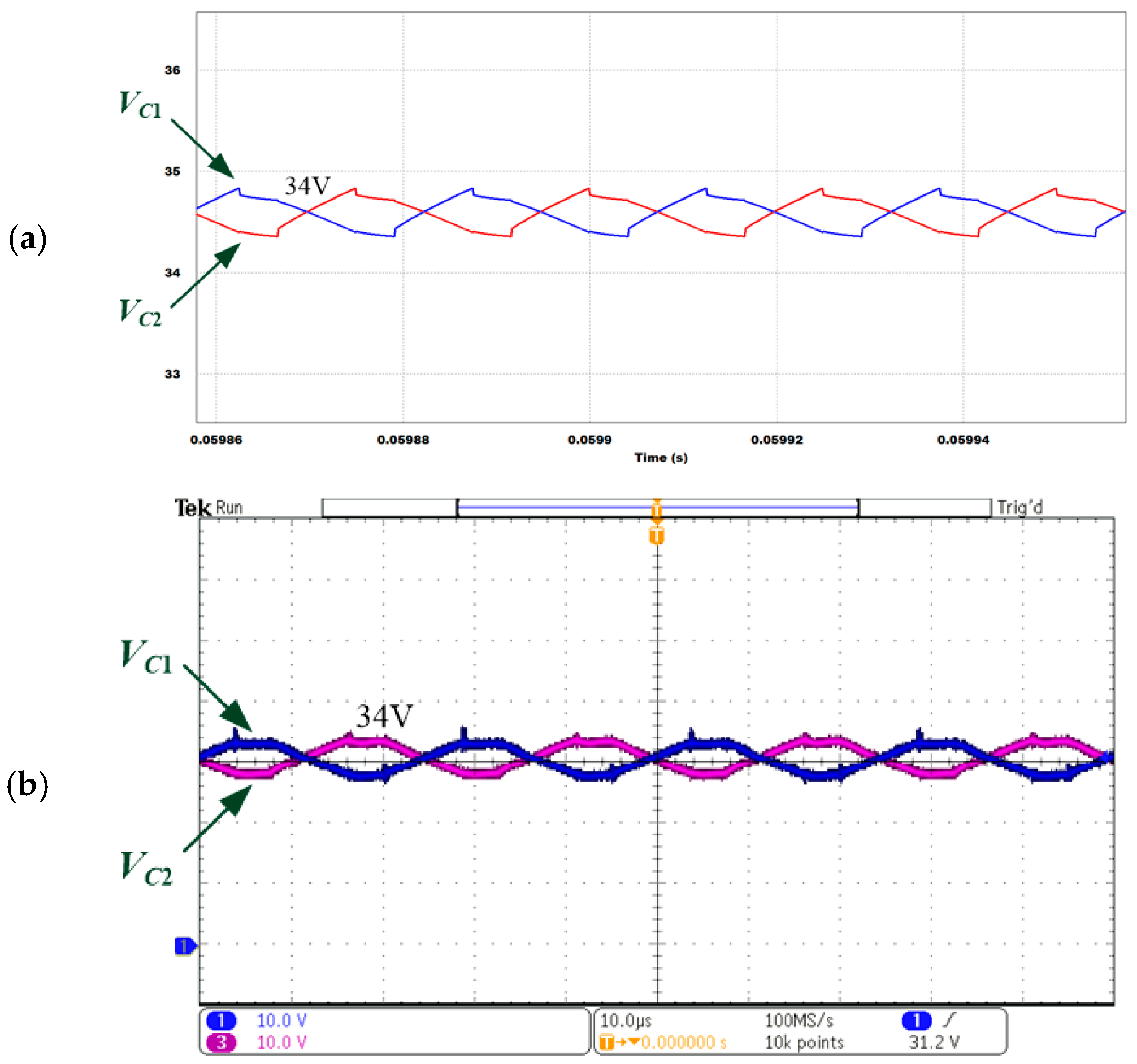
Figure 19.
Waveforms of transient response in the load period steps from 120 W to 60 W and then back to 120 W. (a) Simulated waveforms; (b) Experimented waveforms.
Figure 19.
Waveforms of transient response in the load period steps from 120 W to 60 W and then back to 120 W. (a) Simulated waveforms; (b) Experimented waveforms.

Figure 20.
The measured conversion efficiency for the proposed combined boost converter, the conventional boost converter, and the interleaved boost converter with two-phase.
Figure 20.
The measured conversion efficiency for the proposed combined boost converter, the conventional boost converter, and the interleaved boost converter with two-phase.

Figure 21.
The losses breakdown charts. (a) half load and (b) rated load conditions.

Table 1.
The results for stress analysis in steady-state.
| Items | State |
|---|---|
| RMS current stress on S1 (iS1) | |
| RMS current stress on S2 (iS2) | |
| RMS current stress on L1 (iL1) | |
| RMS current stress on L2 (iL2) | |
| RMS current stress on Lt (iLt) | |
| RMS current stress on D1 (iD1) | |
| RMS current stress of D2 (iD2) | |
| RMS current stress of C1 (iC1) | |
| RMS current stress of C2 (iC2) | |
| RMS current stress of Co (iCo) |
Table 2.
The equations of loss in steady-state.
| Items | State |
|---|---|
| Total loss of S1 | |
| Total loss of S2 | |
| Conduction loss of L1 | |
| Conduction loss of L2 | |
| Total loss of D1 | |
| Total loss of D2 | |
| Conduction loss of C1 | |
| Conduction loss of C2 | |
| Conduction loss of Co |
※ Qg represents the total charge on the gate of the metal-oxide-semiconductor field-effect transistor (MOSFET). The rise time Tr is the time it takes to complete charging the gate of the MOSFET after the threshold voltage VGS(th) has been reached. The fall time, Tf, is the time it takes to reach the threshold voltage following the MOSFET’s switch-off delay time [34]. VF represents the forward voltage drop of the diode. K is the time of the conduction period of the diode. VR represents the reverse voltage of the diode. IR is the reverse leakage current of the diode [35].
Table 3.
Specifications of Converter Prototype.
| Specification | Value |
|---|---|
| Input Voltage, Vi | 12 V |
| Output Voltage, Vo | 60 V |
| Duty Cycle, D | 0.67 |
| Switching Frequency, fsw | 40 kHz |
| Output power, Po | 120 W |
Table 4.
Parameters of Components.
| Specification | Value |
|---|---|
| MOSFET | IPP080N06NG |
| Diode | STPS8H100 |
| Load Resistance, R | 30 Ω |
| Inductors, L1 and L2 | 250 μH |
| Filter Capacitors, C1 and C2 | 10 μF |
| Output Capacitor, Co | 1000 μF |
Table 5.
Parameters of Components.
| Items | Results (50% Load) | Results (100% Load) |
|---|---|---|
| Switching loss of S1 | 0.049 W | 0.059 W |
| Switching loss of S2 | 0.049 W | 0.059 W |
| Conduction loss of L1 and L2 | 0.64 W | 3.2 W |
| Conduction loss of D1 and D2 | 0.0384 W | 0.23 W |
| Conduction loss of C1 and C2 | 0.196 W | 1.02 W |
| Conduction loss of Co | 0.035 W | 0.075 W |
| Total losses | 1.8828 W | 9.134 W |
| Calculated Efficiency | 98.5% | 92.4% |
| Measured Efficiency | 97.3% | 89.1% |
Table 6.
Performance comparisons among other existing converters.
| Items | Topology | |||
|---|---|---|---|---|
| This Converter | [11] | [19] | [24] | |
| Switching control structure | two-phase | single-phase | three-Phase | single-phase |
| Input current ripple | Low | High | Low | Medium |
| Voltage gain | (1 + D)/(1 − D) | (1 + D)/(1 − D) | (3+ nD − D2 )/(1 − D) | 1/(1 − D)2 |
| High-side voltage | 60 V | 60 V | 200 V | 62.5 V |
| Low-side voltage | 12 V | 12 V | 24 V | 10 V |
| Number of main power devices | 4 | 3 | 8 | 4 |
| Number of storage components | 5 | 4 | 8 | 5 |
| Maximum efficiency | 98.7% | 92.1% | 92.3% | 92.5% |
| Realized prototype power rating | 120 W | 40 W | 100 W | 100 W |
| BOM Cost | Low | Low | High | Medium |
Remark-n represents the turns ratio for coupled inductor [19].
© 2017 by the authors. Licensee MDPI, Basel, Switzerland. This article is an open access article distributed under the terms and conditions of the Creative Commons Attribution (CC BY) license (http://creativecommons.org/licenses/by/4.0/).
Share and Cite
MDPI and ACS Style
Lai, C.-M.; Cheng, Y.-H.; Teh, J.; Lin, Y.-C. A New Combined Boost Converter with Improved Voltage Gain as a Battery-Powered Front-End Interface for Automotive Audio Amplifiers. Energies 2017, 10, 1128. https://doi.org/10.3390/en10081128
AMA Style
Lai C-M, Cheng Y-H, Teh J, Lin Y-C. A New Combined Boost Converter with Improved Voltage Gain as a Battery-Powered Front-End Interface for Automotive Audio Amplifiers. Energies. 2017; 10(8):1128. https://doi.org/10.3390/en10081128
Chicago/Turabian StyleLai, Ching-Ming, Yu-Huei Cheng, Jiashen Teh, and Yuan-Chih Lin. 2017. "A New Combined Boost Converter with Improved Voltage Gain as a Battery-Powered Front-End Interface for Automotive Audio Amplifiers" Energies 10, no. 8: 1128. https://doi.org/10.3390/en10081128
Note that from the first issue of 2016, this journal uses article numbers instead of page numbers. See further details here.