High Gain Boost Interleaved Converters with Coupled Inductors and with Demagnetizing Circuits


Department of Mechatronics and Electronics, Faculty of Electrical Engineering, University of Zilina, Zilina 010 26, Slovakia
*
Author to whom correspondence should be addressed.
Energies 2018, 11(1), 130; https://doi.org/10.3390/en11010130
Submission received: 15 November 2017
/
Revised: 13 December 2017
/
Accepted: 3 January 2018
/
Published: 5 January 2018
(This article belongs to the Special Issue Emerging Power Electronics Technologies for Power Systems and Machine Drives)
Abstract
:This paper proposes double interleaved boost converters with high voltage gain and with magnetically coupled inductors, while a third coupled winding is used for magnetic flux reset of the core during converter operation. The topology of the proposal is simple, it does not require many additional components compared to standard interleaved topologies, and it improves the transfer characteristics, as well as system efficiency even for high power levels. The investigation of steady-state operation was undertaken. It was discovered that the proposed converter can be designed for a target application where very high voltage gain is required, while adjustment of voltage gain value can be done through duty-cycle variation or by the turns-ratio modification between individual coils. The 1 kW prototype was designed to test the theoretical analysis. The results demonstrate that the proposed converter achieves very high voltage gain (1:8), while for the designed prototype the peak efficiency reaches >96% even when two additional diodes and one winding were implemented within the converter’s main circuit. The dependency of the output voltage stiffness on load change is minimal. Thus, the presented converter might be a proper solution for applications where tight constant DC-bus voltage is required (a DC-DC converter for inverters).
1. Introduction
Current trends in automotive applications are characterized by a common rule—green energy, or blue energy. More and more non-conventional energy systems and powered electronic systems are used within the internal infrastructure of vehicles, whose energy storage and conversion systems are still transforming and being optimized as electric vehicles are being considered. The main reasons are efficiency, reliability and power density. Worth mentioning are energy storage systems, drive systems, fuel cells, solar panels, electronic devices for energy conversion etc. Most of the green energy systems are of low output voltage. If practical use of such devices is required or requested, then a proper conversion system must be used, i.e., low voltage energy source must be boosted to the values that are necessary for other electronic devices (power inverter and electric machine for example). For application within a power train of electric vehicles it is required to boost 80 VDC/120 VDC to the values that are required for electric driving, i.e., 400 VDC. Therefore, a boost converter must be used.
Conventional boost converters have limits that are related to voltage gain, power capability and efficiency. In other words, when high voltage gain is required, the converter may operate at an unacceptable duty cycle, which results in a very high voltage stress of devices, and conversion loss of the circuit will ensue. For that reason, perspective topological modification has been made. Most of the proposals are focused on the optimization of the voltage gain ratio in the pursuit of duty cycle improvement [1,2,3,4,5]. Many single-stage high voltage gain converters have been developed [6,7,8,9,10] with switched capacitors [11,12,13,14,15,16]. Interleaved topologies with coupled inductors [17,18,19,20,21,22] or with voltage lift techniques have been proposed [23,24,25]. However, there still exist several disadvantages that might be further optimized in order to improve the electrical behavior at the power stage, which deal with power limit when interleaved topology is considered, while voltage gain is limited at high powers because of the conduction losses of the circuit, which increase by an extreme amount at high power levels together with losses of magnetic material, which are also a limiting factor when saturation or DC biasing comes into account [26,27,28,29,30]. Almost magnetic components are very important parameters, and attention must be paid for perspective proposals when interleaved boost topology is considered. The inductors of interleaved boost converters, which are magnetically coupled, are continuously saturated by DC current components. The variable that is the most negatively affected in this case is efficiency.
This paper proposes a double interleaved boost converter with high voltage gain and with magnetically coupled inductors, while a third coupled winding is used for magnetic flux reset of the core during the converter operation as well as for the voltage gain adjustment. The topology of the proposal is simple, it does not require many additional components compared to standard interleaved topologies [31,32,33,34,35] and it improves the transfer characteristics, as well as system efficiency even for high power levels [36]. With its superior behavior related to the output voltage stiffness in dependency on load change, it might be a proper solution for applications where constant DC-bus voltage is required (DC-DC converter for inverters). The main focus within this paper is given to the steady state analysis, voltage transfer characteristic derivation, magnetic component stress reduction and system efficiency identification.
2. Dual Interleaved Boost Converter with Magnetically Coupled Inductors and with Demagnetizing Circuit
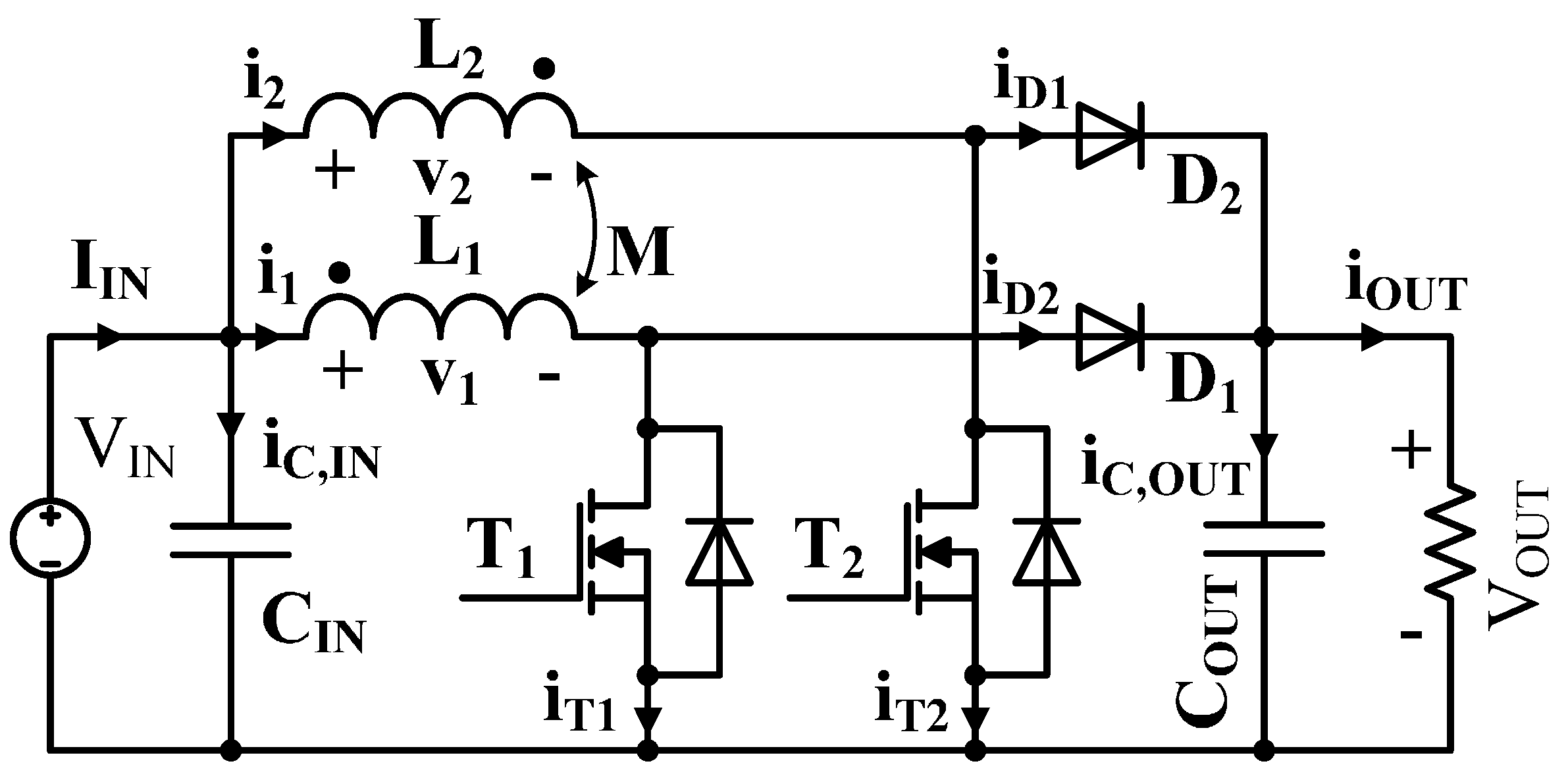
Figure 1 shows the dual interleaved DC-DC boost converter with magnetically coupled inductors. Analysis of the DC-DC converter (Figure 1) is primarily done under operation in the CCM mode, so that the currents i1 and i2 are always positive. The advantages of CCM operation against DCM operation include the minimization of circuit ringing, inductor and input ripple current reduction, and voltage ripple effects elimination as well as elimination of their associated mitigation. Waveforms from steady state operation of dual interleaved boost converters for CCM operation with a duty ratio greater than 0.5 (while duty cycle of T1 and T2 is equal), are shown in Figure 2. It shows input current (iIN), inductor voltages (V1, V2), inductor currents (i1, i2), and T1 and T2 gate drives. For CCM operation, the voltage gain is the same as that given for a simple boost converter described by (1).
where VOUT is output voltage of the converter, VIN is input supply voltage and D is the duty cycle.
It is observed that the voltage gain is primarily dependent on the duty cycle of the converter operation.
The standard solution to dual interleaved boost converters with magnetically coupled inductors has its advantages compared to the classic boost converter. They apply even when higher power demands are given on the power stage. Instead of that, reduction of voltage and current ripple enable a reduction in passive components, even when a high switching operation is considered. However, on the other side, some disadvantages arise and are related to the voltage gain and magnetic design and operation of coupled inductors. During each operating cycle, the DC component of the current of each winding (L1 and L2) exists. This limits the magnetic component to be used for higher power, and bulky magnetic core or special geometry modifications must be used in order to prevent saturation of the magnetic core. In the same way, the efficiency is affected and can be decreased when wrong magnetic design is performed.
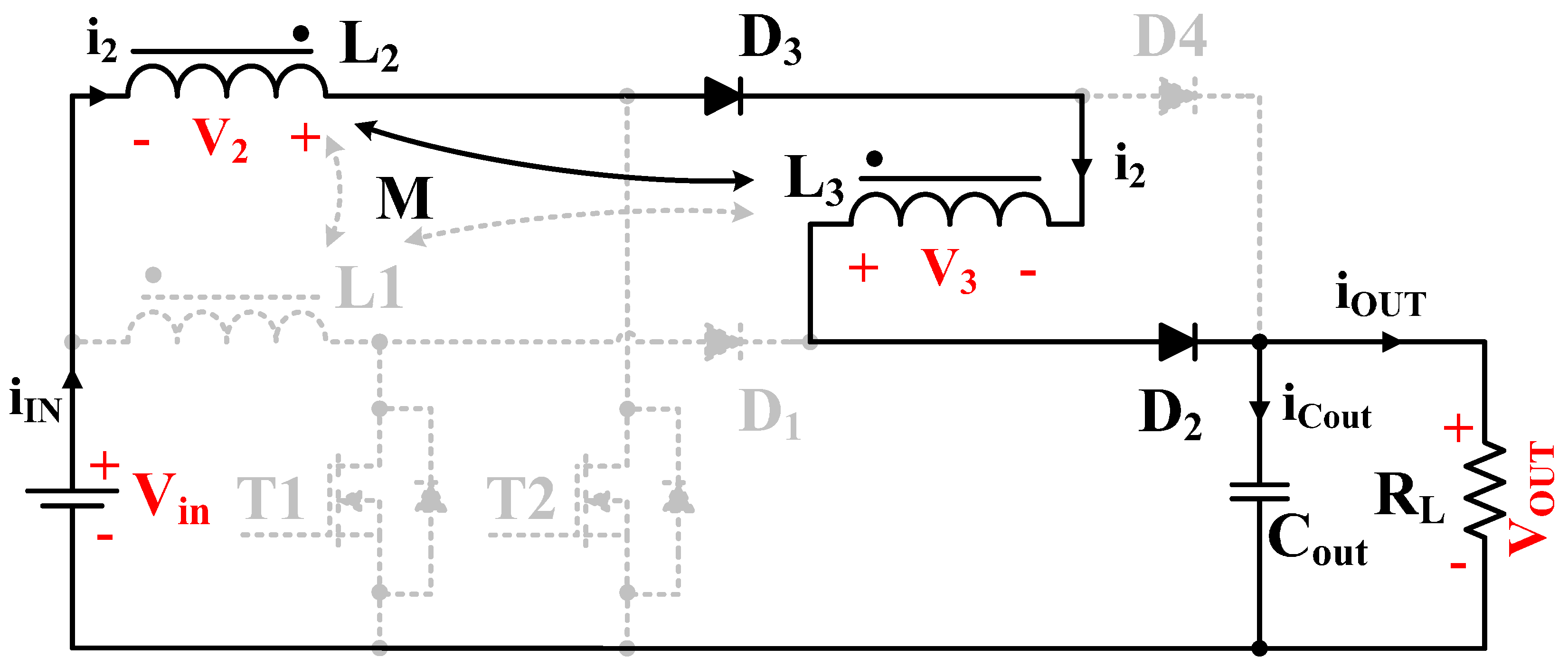
The proposed interleaved boost converter with magnetically coupled inductors and with demagnetizing circuit is shown in Figure 3. It is composed of a standard double interleaved boost converter (Figure 1), where a demagnetizing circuit, which consists of L3-D4-D2 is added to the output part of the proposed converter. This demagnetizing circuit also creates an additional pseudo transformer within the proposed converter circuit, and as will be seen later, the ratio between boost inductances (L1, L2) and demagnetizing inductance (L3) influences the voltage gain. The proposed converter is voltage gain independent on the duty cycle operation in wide operational range, and thus constant output voltage within wide range of output load can be achieved.
The switching operation is similar to the standard interleaved converter, i.e., transistors T1 and T2 are switching in an interleaved manner with given dead time. Inductor L3 is magnetically coupled altogether with L1 and L2 and serves as a demagnetizing snubber whose effect applies during each switching action of each transistor. In this configuration, it servers as an AC magnetic flux reset inductor. The current flow I3 during each operation cycle is opposed to the current of inductors L1 and L2. This enables a reduction in the magnetic core saturation, thus the DC component of the inductor currents can be eliminated.
3. Operational Analysis of Proposed Converter
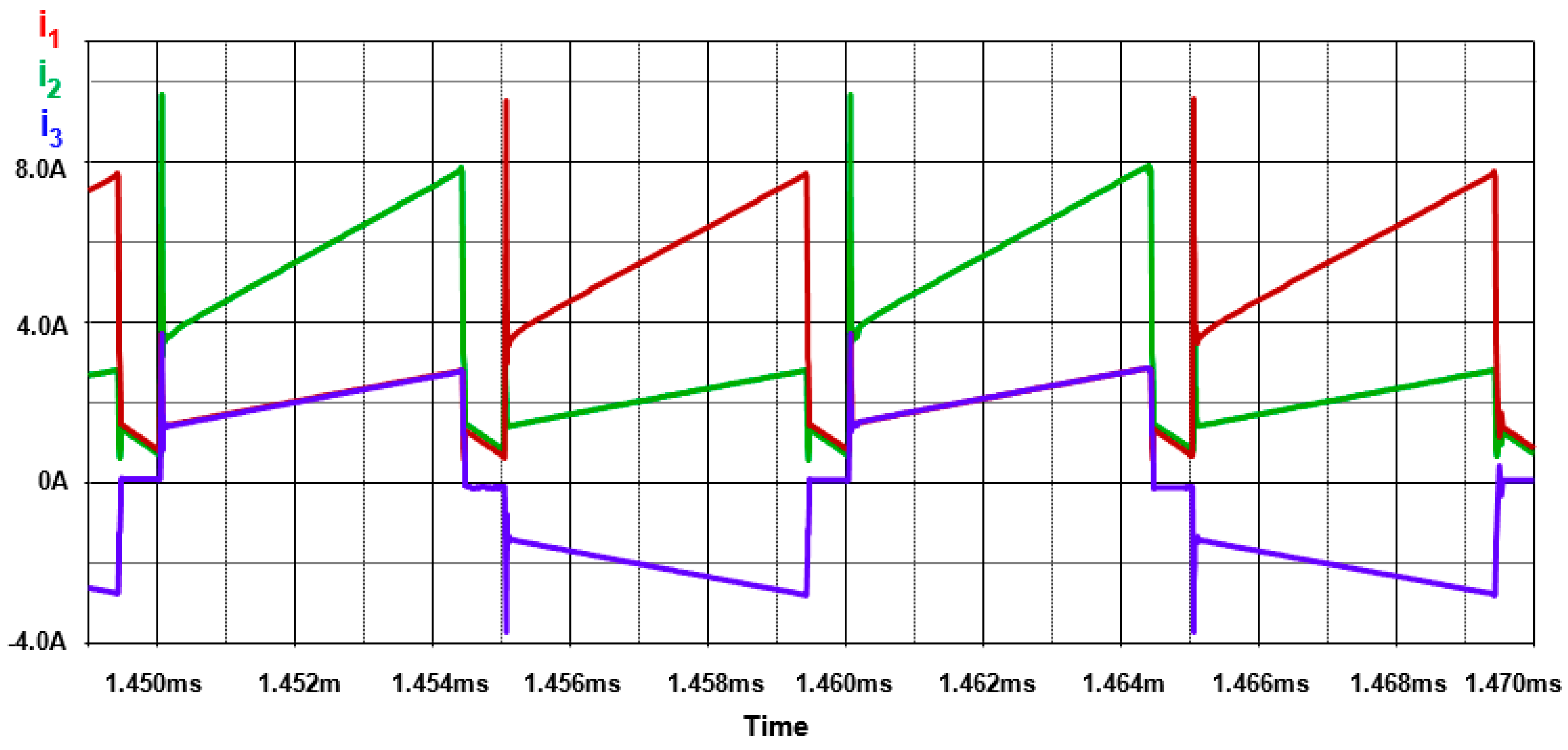
The operation of the dual interleaved boost converter with magnetically coupled inductors and with demagnetizing circuits can be divided into four operational intervals. One switching cycle can be then understood as in an ON and OFF state after consequent switching of transistors T1 and T2. Thus, 2 active and 2 passive intervals exist. For initial investigation of converter operation it can be assumed that the duration of active interval will be equal to the duration of the passive interval. The switching driving signals for this situation are shown in Figure 4. It is also considered that the turns ratio between individual coils is equal to 1:1:1, so all inductors have the same value. The operational waveforms for analyzed steady state are shown on Figure 5.
3.1. Working Intervals of Proposed Converter
The operation of the converter can be divided into four consecutive intervals, which periodically repeat. The initial analysis of the operation is done for the conditions where L1 = L2 = L3 = L, and M1 = M2 = M3 = M. The operation of the converter shall be considered within steady-state operation.
3.1.1. Interval (Active—T1—ON, T2—OFF)
Initial conditions:
- -
- T1—ON,
- -
- T2—OFF (the transistor T2 was before this interval in conduction state, thus L2 is accumulated with the energy),
- -
- D2, D3—conducting,
- -
- L1 is accumulating the energy,
- -
- L2 and L3 are transferring energy into output capacitor COUT and to the load RL.
This interval (Figure 6) starts after turn-on of T1, while its ON-period is equal to the half of the half period cycle, i.e., tON1 = D1 × T/2, whereby D1 = 0.25. The current in the inductor L1 linearly rises, while the current in the inductors L2 and L3 is linearly decreasing and is half the value of current i1. The voltage on the coil L1 is the opposite polarity to the voltages on inductors L2 and L3. Using Kirchhoff’s second law, it is possible to derive dependency of the output voltage on the inductor voltages. For the first-time interval of the converter’s operation, the following equations are valid:
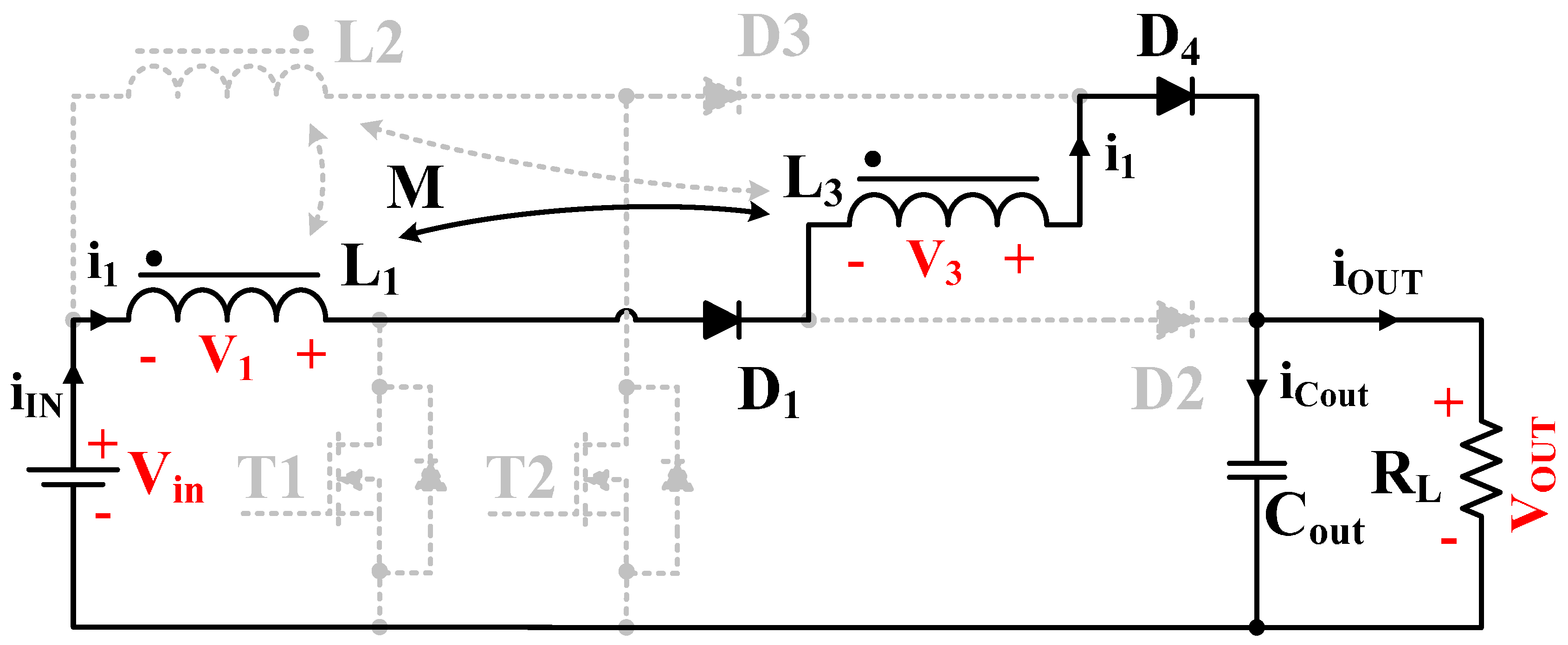
3.1.2. Interval (Passive—T1—OFF, T2—OFF)
Initial conditions:
- -
- T1—OFF,
- -
- T2—OFF,
- -
- D1, D4—conducting,
- -
- L1 and L3 are transferring energy into output capacitor COUT and to the load RL.
This interval (Figure 7) begins after the transistor T1 turns off. Duration of this interval is tOFF1 = (1 − D1) × T/2. This causes the polarity of the voltages on each inductor to change its polarity to the opposite value compared to the first interval. During this time interval, the current of inductor L2 is equal to zero, because it is not connected to the main circuit. The current of the inductor L1 flows also through the inductor L3, while inductor L1 acts as the source, thus its i1 is linearly decreasing, whereby i3 is linearly increasing. This interval can be characterized by the demagnetizing action of the common magnetic core, because inductor L3 is acting in the opposite direction to the inductor L1. It might be seen that within 1st and 2nd interval of the operation, the AC current is flowing through the L3. The equation of the loop voltages within the main circuit during this time interval is given by (10), while the output voltage is defined by (11).
3.1.3. Interval (Active—T1—OFF, T2—ON)
Initial conditions:
- -
- T2—ON,
- -
- T1—OFF,
- -
- D1, D4—conducting,
- -
- L2 is accumulating the energy,
- -
- L1 and L3 are transferring energy into output capacitor COUT and to the load RL.
The third (Figure 8) interval is again the active interval, and its initialization is characterized by the turn on of the transistor T2, while transistor T1 is still turned off. This interval has the same ON period as the first one, i.e., tON2 = D2 × T/2, where D2 = 0.25. The polarity of the inductor voltages is unchanged compared to 2nd interval. Because direction of the current flow in L3 is unchanged, and its current is linearly increasing from negative values, inductor L1 is continuously acting as the voltage source, thus its current is linearly decreasing with the same slope as current i3 rises. Inductor L2 is being charged as in the case of standard boost converter. It is seen that the 3rd operational interval is similar to the 1st interval, while the only difference is the polarity and behavior of current i3. Therefore based on the loop voltages, the equation for this time interval is given by (14), and consequently dependency of the output voltage is given by (18).
3.1.4. Interval (Passive—T1—OFF, T2—OFF)
Initial conditions:
- -
- T1—OFF,
- -
- T2—OFF,
- -
- D2, D3—conducting,
- -
- L2 and L3 are transferring energy into output capacitor COUT and to the load RL.
The 4th interval (Figure 9) is a passive interval and from the operational point of view it is again comparable to the 2nd interval of the converter’s operation, thus duration is tOFF2 = (1 − D2) × T/2. Start of the interval is characterized by the turn-off action of transistor T2; transistor T1 is still in non-conductive state. The voltages on each inductor change their polarity compared to previous operational interval, thus inductors L2 and L3 are now acting as sources so their currents are linearly decreasing with the same ratio. Inductor L2 is disconnected from the main circuit during this time interval, thus its current is equal to zero. The equation for final operational interval with steady state operation is given by (22). Dependency of the output voltage is given by (23).
Based on the previous analysis, it is seen that the proposed converter has advantages related to the voltage gain, which is dependent on the duty cycle of the converter. Instead of that, the converter is able to operate in a wide range of load, while output voltage is not affected and the only voltage decrease of VOUT is caused by the voltage drop on the individual parasitic components. Voltage ratio between VIN and VOUT can also be adjusted by the ratio between number of turns of the boost inductances (N1 = N2), and number of turns of AC demagnetizing inductance. The process of the determination of the turns ratio between individual inductances (L1–L3) is determined by the requirements of the converter operation, i.e., CCM, DCM, BCM mode. Therefore the inductances L1 and L2 are selected based on the standard procedure for interleaved converter [19,20,22]. The value of the L3 inductance is then determined by the requirements on the voltage gain of the converter. Table 1 shows voltage gain of the proposed converter for pre-defined multiples of the turns of inductances. It is the voltage gain related to the change of inductance ratio, while duty cycle is considered to be within the previous analysis, i.e., D1 = D2 = 0.5.
3.2. Loss Distribution Analysis
Energy losses in elements of the boost converter can be divided into inductor losses, power switch losses and diode losses [37,38,39,40]. Total energy losses PTOT is expressed as:
3.2.1. Inductor Losses
The estimation of the inductor losses is basically the same as that of the transformers. The conduction losses PLCON are:
where RL is serial resistance and IL is current of L.
The core losses (Steinmetz equation) PLMAG are:
where VCORE is the volume of the magnetic core, ΔBL is the flux swing, fSW is switching frequency, k, αCORE, βCORE are the Steinmetz coefficients, which are provided by the manufacturer.
Then the losses of inductor are attained as:
3.2.2. Power Switch Losses
The losses of power switches mainly comprise the switching loss, conduction loss free-wheeling diode loss and the drive loss. The switching losses PTSW are:
where ETON, ETOFF are MOSFET turn-on and switch-off energy.
The conduction losses PTCON are:
where RDSON is on-state resistance and IT is current of power switch.
The free-wheeling diode losses PTFWD are:
where vD0 is diode on-state zero-current voltage, IFAV is average diode current, RD is diode on-state resistance, IFRMS is RMS value of the diode current, EDON is diode energy during MOSFET switch-on transient.
The drive losses PTDRI are:
where QGD is storage charge between the gate and drain, VG is gate voltage.
Then the losses of power switch are attained as:
3.2.3. Diode Losses
The diode losses only contain the switching loss and conduction loss. The switching losses PDSW are:
where VR is diode applied voltage, IR is diode reverse current, T is switching period, tOFF is diode off-time, ERR is switching energy loss due to reverse recovery.
The conduction losses PDCON are:
where VF is diode forward voltage, IF is diode forward current, tON is diode on-time.
Then the diode losses are attained as:
Based on the circuit parameters and circuit components, the determination of individual losses can be realized (Table 2). These losses are valid for 1 kW output power of the proposed converter, supplied from 100 VDC, voltage gain equal to 3.6, with operating frequency 100 kHz.
4. Simulation and Experimental Analysis of the Steady-State Operation
Initial investigation the analysis of the steady state operation is provided, in order to validate operational characteristics of the converter. In this study, these are related to the output characteristic (dependency of output voltage on the output power at constant duty cycle), efficiency characteristic (dependency of system efficiency on the output power at constant duty cycle), and voltage gain characteristic, i.e., dependency of the output voltage on the duty cycle at various output powers. Finally, the analysis of the voltage gain characteristic on the inductance ratio was performed, while the duty cycle is constant. The input-output condition of the simulation as well as of the experimental measurement are defined as follows, whereby OrCAD–Pspice was used for simulation analysis:
- -
- VIN = 100 V
- -
- Switching frequency (fSW) = 100 kHz
- -
- VOUT = expected based on voltage gain = 400 V
- -
- POUT = 1 kW (2.5 A)
- -
- Duty cycle = D1 = D2 = range 0.1–0.45
- -
- Voltage gain = 3.6 (N1 = N2 = 6, N3 =10 ≥ TR = 1:1.7)
- -
- Inductor core = feroxcube EI43/3F3 planar
- -
- Power transistors = Cree C3M0065100K
- -
- Power diodes = STPSC1206D
- -
- Input capacitors = 3 × 390 µF/160 V SAMWHA
- -
- Output capacitors = 4 × 22 µF/450 V Wurth Electronic
The experimental prototype of the proposed converter is shown on Figure 10. The four-layer PCB was used for power stage. Control stage is realized with the universal board equipped by MCU, in order to provide various experiments related to the investigation of the steady-state performance. The integrated interleaved magnetics is equipped within planar technology, whereby EI E43 3F3 planar core was used.
4.1. Steady State Operation—Principal Waveforms
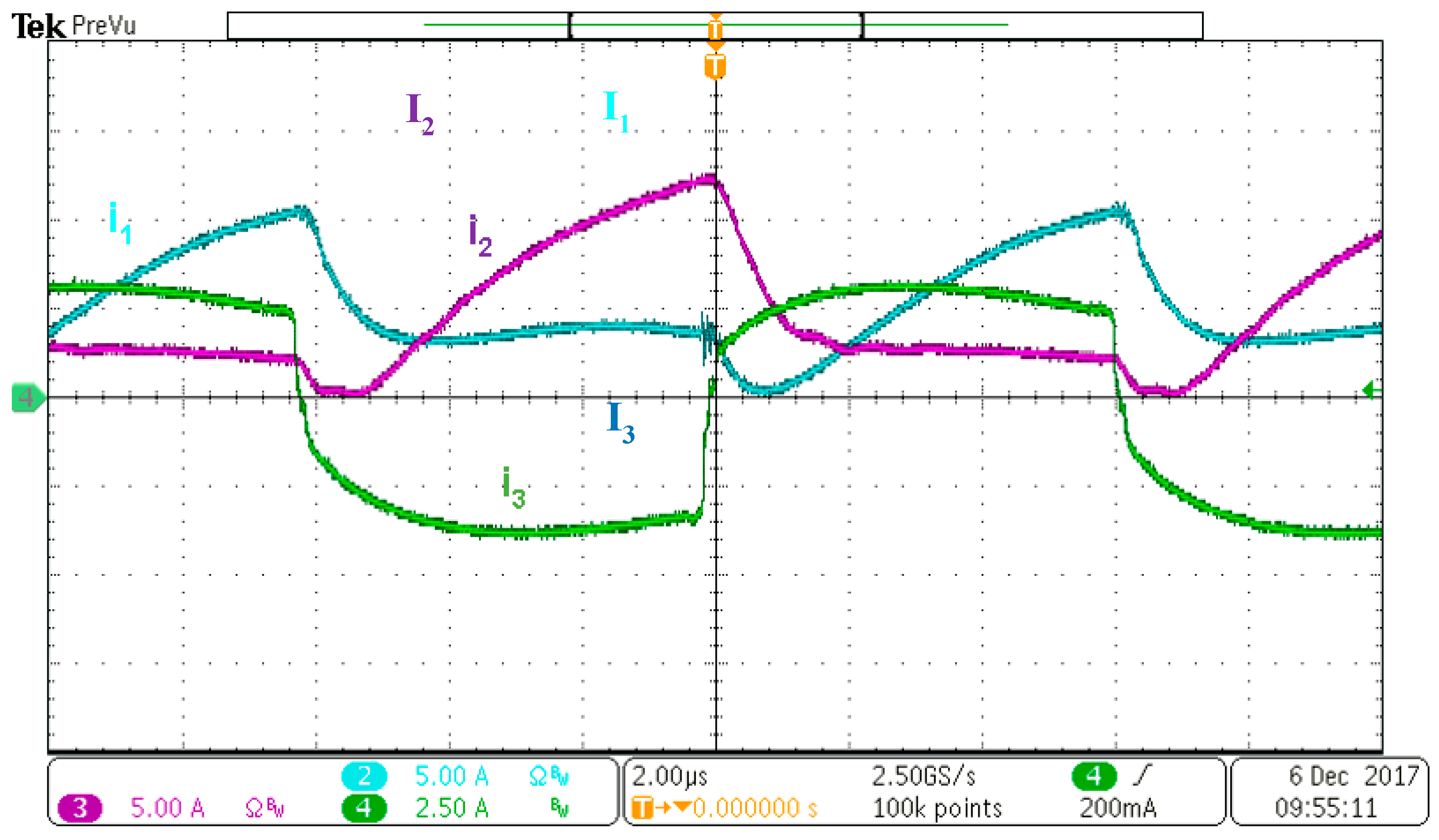
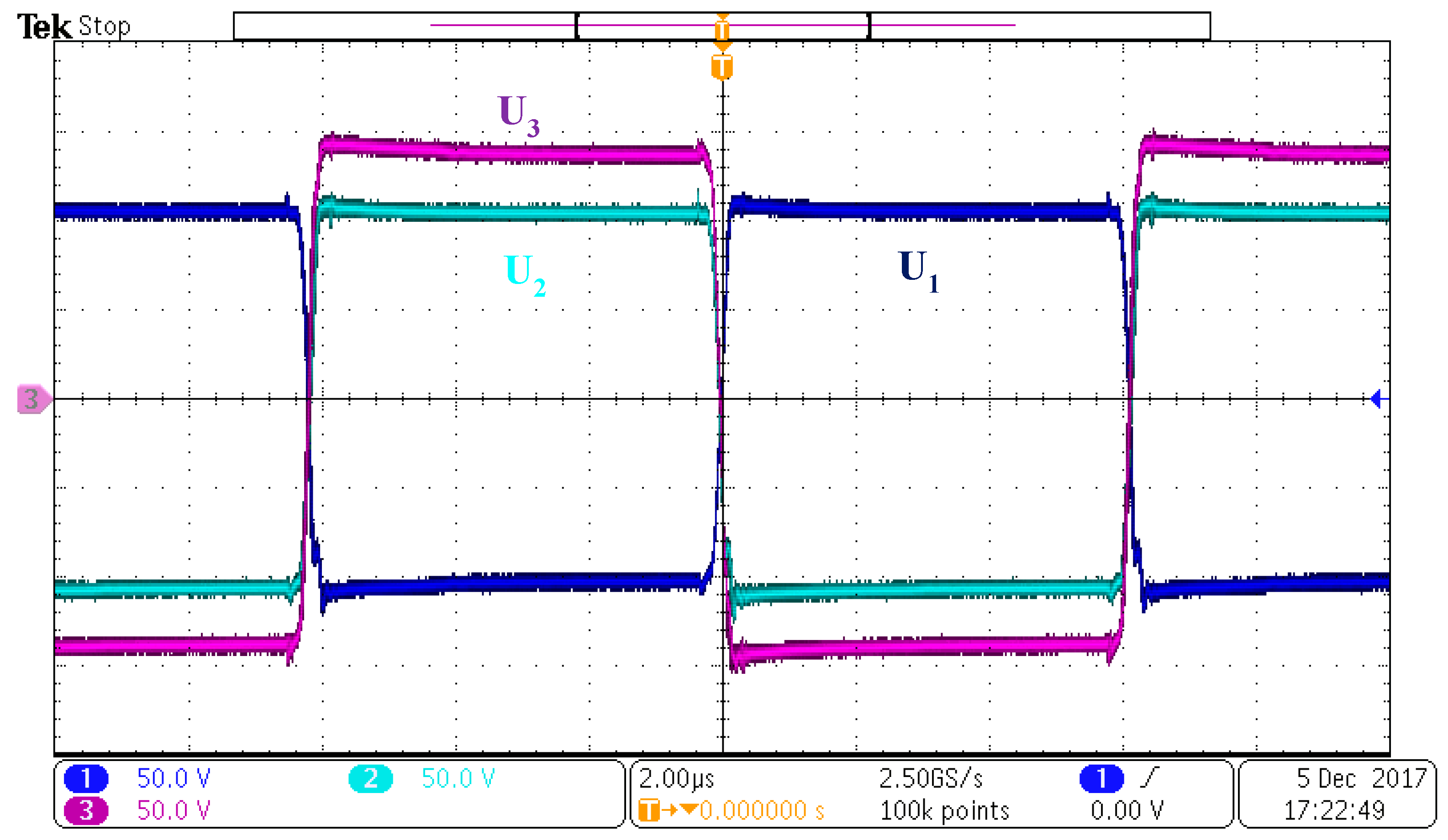
Initial experiments were performed in order to investigate the operational waveforms on the individual main components of the proposed converter within steady-state operation. Comparisons between simulation and measurements are given. Figure 11 and Figure 12 show current waveforms of individual inductors. It is seen that the current of the boost inductors L1 and L2 has DC offset and is of DC character. This fact may saturate the core of the inductor because of the existence of the DC component, but as can be seen, current through the reset inductor L3 is a product of the current i2 and i1 and has AC character. Therefore the core of the proposed converter will not be saturated by the DC component, which is beneficial because a lower volume of the inductive component can be used, or higher power at the same size can be delivered considering an alternate interleaved converter.
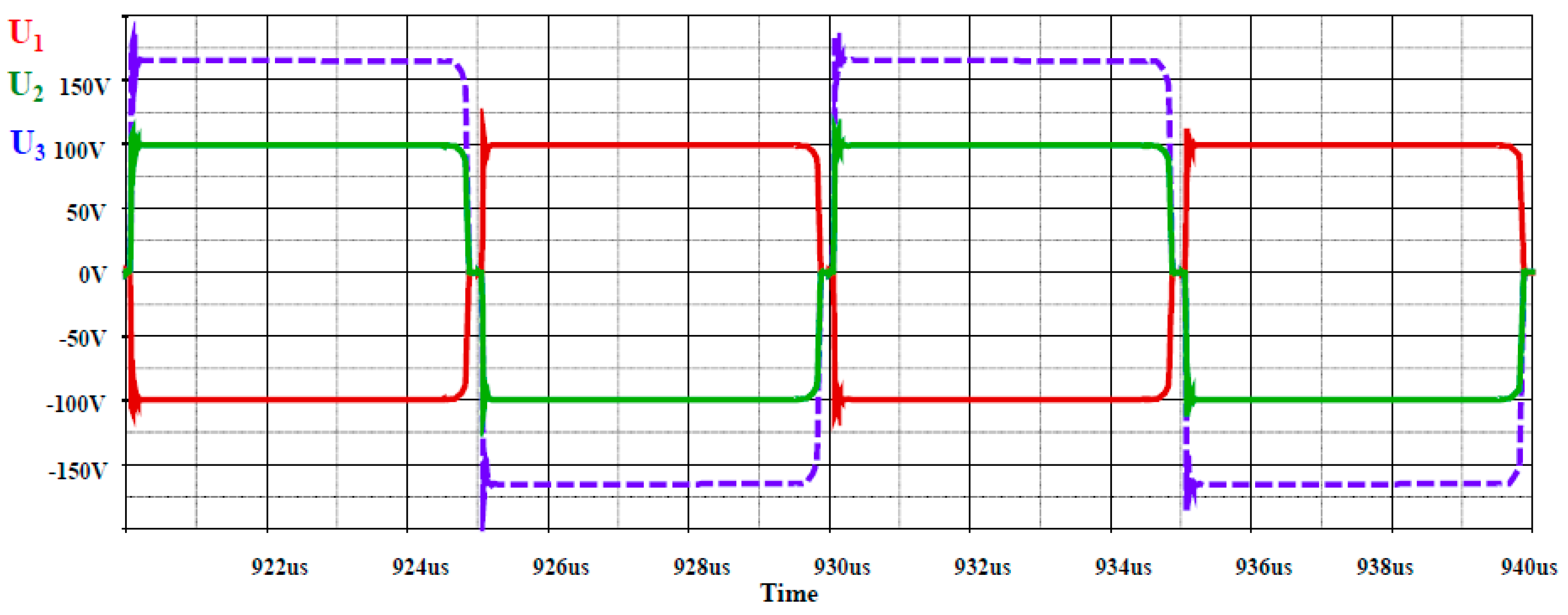
Figure 13 and Figure 14 show the voltage waveforms on the individual inductances. It is seen again that the voltage on the L3 is of different amplitude compared to the both voltage waveforms on the L1 and L2. This is relevant to the voltage gain modification through the turn ratio. In this case, it was set to 10:6, thus the voltage on the inductance L3 shall be 1.6 times higher the voltages on the inductances L1 and L2, whose amplitude is equal to the amplitude of the supply voltage. This is confirmed both by the simulation and by the measurement.
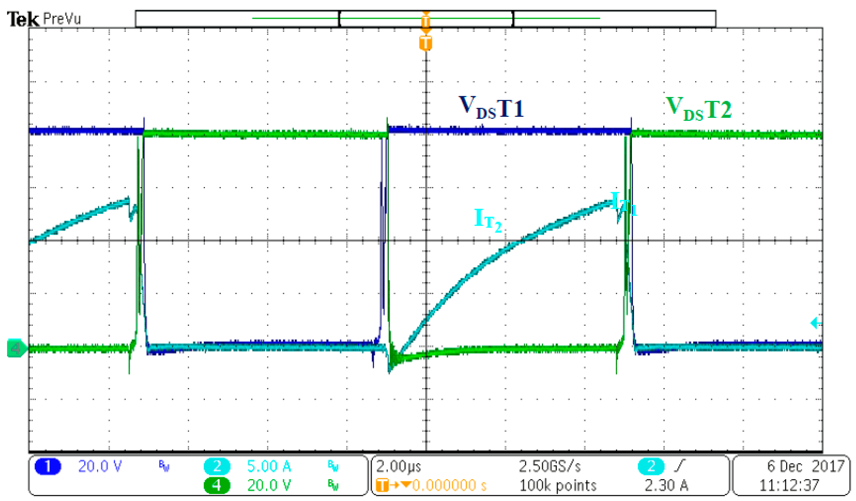
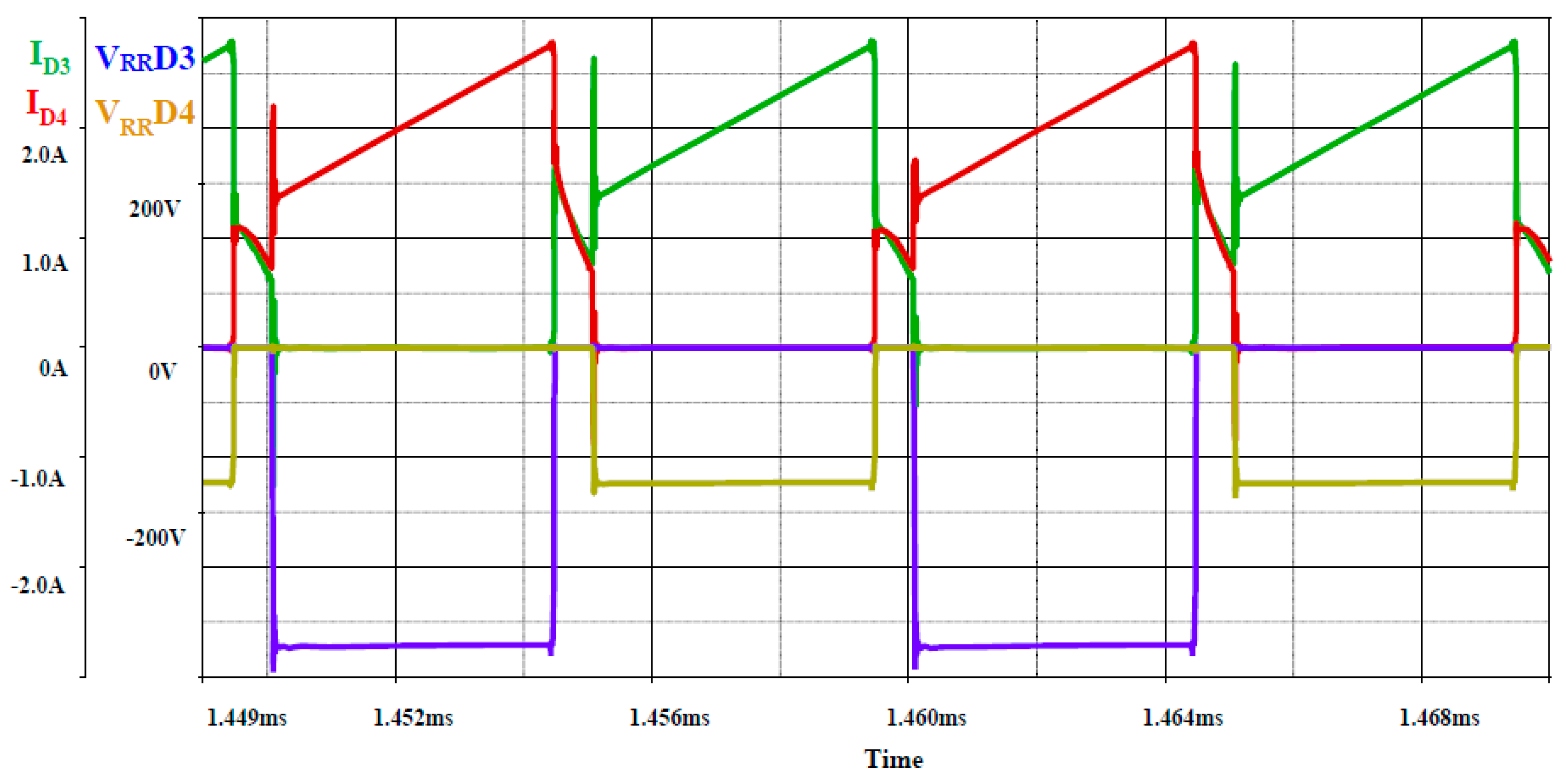
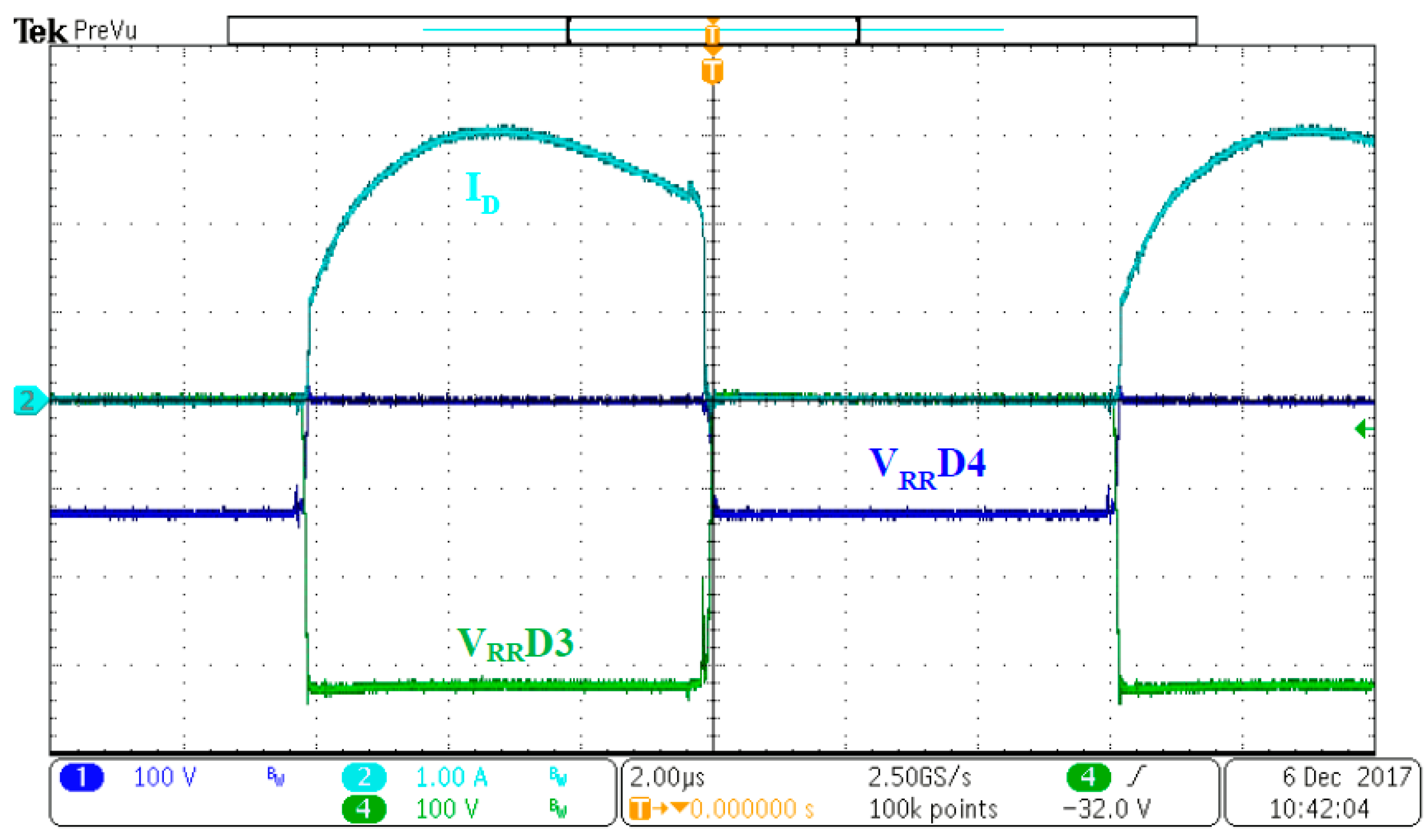
Figure 15, Figure 16, Figure 17 and Figure 18 show current and voltage waveforms of the semiconductor devices. The converter is operating in the hard-switching mode, while waveforms are relevant to the basic operational characteristics of the boost converter. Thus, switching losses will be the most important part of the losses affecting the system efficiency. For that purpose, the proper selection of semiconductor devices will be important, or implementation of the soft switching technique shall also be considered.
Further investigation of the proposed converter is focused on the efficiency behavior within whole operational range, i.e., at various power levels and consequently the identification of the voltage transfer characteristic is done in dependency on the duty cycle, as well as on the value of turn’s ratio.
4.2. Operational Characteristics
4.2.1. Efficiency, Output Voltage = f (Output Power), Duty Cycle = Constant
Within this part of investigation several measurements were taken in relation to the efficiency performance, and output characteristic of the proposed converter was investigated. The measurements were taken for the variable power at constant duty cycle, i.e., at D1 = D2 = 0.45. Change of load was in the range of 10–100%. Table 3 shows individual values of the efficiency and the value of the output power in dependency on the output power. This is graphically interpreted in Figure 19.
It is seen (Figure 19) that the efficiency curve is flat when considering whole operating range, and system efficiency is not below 90%. This is a beneficial behavior for low-load conditions, whereby maximum efficiency is achieved at around the point of the maximal power, i.e., at 900 W, where efficiency is above 96%. It can be seen that the value of output voltage is not affected when considering the change of the output power. The converter has stiff behavior when the voltage drop from low load to the full load is 4 V. This behavior is highly valuable in applications where stiff DC voltage is required, i.e., for a DC bus for inverter stage.
Figure 20 shows power loss analysis based on Equations (26)–(37). The total calculated power loss is 40.53 W (Table 3) within the peak efficiency of the converter (96.2%). At nominal output power, the efficiency of the converter is 95.5%, which is related to the power losses at the value of 47.15 W. Because the proposed converter operates at hard-switching commutation mode, the highest portion of the losses belongs to semiconductor devices (more than 85% of total losses belong to switching losses). Therefore, proper selection of transistors and diodes are critical for efficiency performance of the proposed converter.
4.2.2. Voltage Gain = f (Duty Cycle), Output Power = 100%, 20%
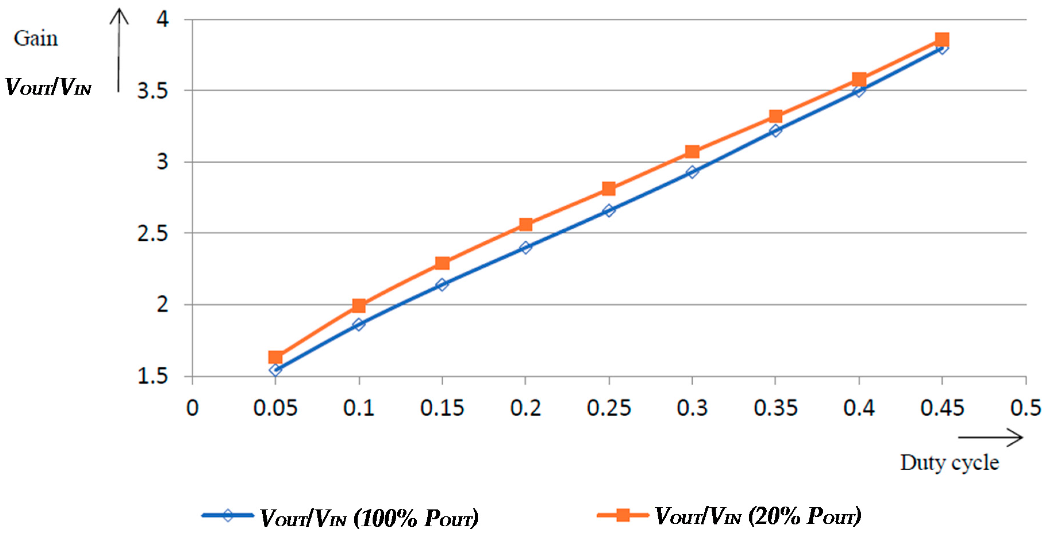
Consequently, the investigation of the voltage gain in dependency on the duty cycle was performed. The results are listed in Table 4, wherein two situations have been considered. The power load of 20% and 100% was defined within measurements. From the table it can be seen that the change of the load has very low effect on the change of the value of voltage gain. The voltage gain characteristic in dependency on duty cycle is shown on Figure 21. At a given turns ratio, the voltage gain can be adjusted through the duty cycle modification in the range of 1.5–3.8.
4.2.3. Voltage Gain = f (Inductance Ratio), Duty Cycle = Constant
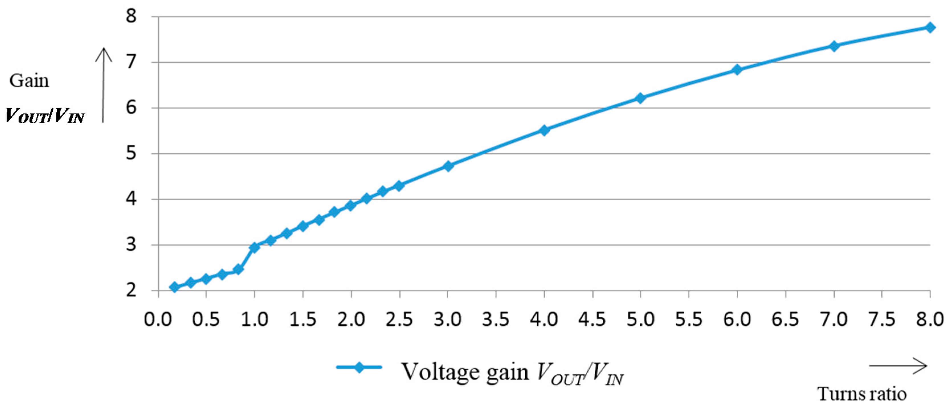
The last investigation within the steady-state performance of the converter related to the voltage gain characteristic was realized by way of the turn’s ratio modification. Within this experiment the number of turns on the boost inductors L1 and L2 was left constant, while the change of the turns on the reset inductance L3 was provided. The duty cycle within this experiment was constant and equal to D1 = D2 = 0.45. The range of the turn’s ratio was done within 1–8. The following Table 5 and Table 6 show the dependency of the voltage gain on the turn’s ratio. It can be seen (Figure 22) that this dependency is in linear relationship, thus with the increase of the turns on the reset inductance, the higher voltage gain can be achieved. It is a beneficial property of this proposed converter’s topology, because the range of the output voltage can be considerably increased.
4.3. Comparisons of Proposed Converter Performance to Other Circuit Alternatives
The given properties of the proposed converter are compared to the standard dual-interleaved boost type converter and to the classic boost converter. The input–output parameters are considered to be similar to those specified at the beginning of chapter 4, thus 1 kW output power supplied from input voltage source 100 VDC, switching frequency is 100 kHz. The voltage gain of all converters was set to VOUT/VIN = 3.6. The results from the analysis related to the operational parameters/characteristics are listed in Table 7.
From Table 7 it is seen that the proposed converter has advantages related to the overall efficiency rated at full output power; even the number of components is higher. This is related to the fact that much a lower magnetic core can be used, while its performance is improved also by the fact that the AC component is continuously flowing through its circuit. In this way, core losses and hysteresis losses are much lower, because DC magnetization is eliminated. The value of bulky output electrolytic capacitor can be more than 10 times lower compared to the standard solution, and through this it is possible to eliminate losses related to parasitic ESR of electrolytic capacitor. Even when the value of capacitor of the proposed converter is very low, the output voltage ripple is more than 10 times lower compared to the interleaved boost converter and more than 25 times lower compared to the standard boost converter. The advantages are also related to the input current ripple, while due to the existence of an AC component in the circuit, the current ripple can be minimized compared to standard topologies. On the other hand, it is seen that the voltage gain of the proposed converter has limitations compared to other topologies, which is related to optimal selection of turns ratio between inductances L1, L2 and L3.
5. Conclusions
Within this paper a new perspective topology was introduced. It is an interleaved boost converter with the core reset additional inductance. The existence of this inductance enables within each operational period of the converter a reset of the magnetic core, where all inductors are implemented. The AC waveform of the current flows through this inductance, thus the saturation of the core by the DC component is not critical, as opposed to the other standard interleaved boost topologies.
The steady state operation is described in more detail, while the main focus was placed on the efficiency, and voltage gain performance. It is seen that efficiency is competitive in the whole operational range, with the best-in-class topologies of power converters. Further improvements can be done with the implementation of a soft-switching technique, which will be the task for the future work. Voltage gain can be modified two ways, i.e., with the change of the duty cycle, or with the selection of the turns ratio between boost inductances and reset inductance. This feature will be valuable in applications where very high voltage gain is required. On the other hand, special focus must be given to the integrated magnetics design; this will also be a topic of the future research. Meanwhile, the highly advantageous characteristic of the proposed converter is its very tight output voltage character in the whole power range. This feature is highly appreciated in applications, such as the DC bus circuit, where requirements for stable voltage are given.
As mentioned, future work should focus further on efficiency improvements, and also on the dynamic and control analysis.
Acknowledgments
The authors would like to thank for the support to the Slovak National Grant Agency APVV for project APVV-0396-15—New generation of power supplies utilized GaN technology, and to Slovak National Grant Agency VEGA for project Vega-1/0479/17—Research of optimal control methods for optimal energy transfer in storage systems. The special thank is also given to the BH Motorsport company for specific material support and supplementary equipment support.
Author Contributions
Michal Frivaldsky prepared the paper structure and has organized individual works within the paper preparations, made simulation analysis and finally he wrote the paper. Branislav Hanko has designed experimental prototype of proposed converter and has organized initial measurements. Michal Prazenica is responsible for the mathematical analysis and power loss analysis of the proposed converter. Jan Morgos was realizing the experimental verification and analysis of the data from simulations as well as from experimental measurements.
Conflicts of Interest
The authors declare no conflict of interest.
References
- Lee, J.-P.; Cha, H.; Shin, D.; Lee, K.-J.; Yoo, D.-W.; Yoo, J.-Y. Analysis and Design of Coupled Inductors for Two-Phase Interleaved DC-DC Converters. J. Power Electron. 2013, 13, 339–348. [Google Scholar] [CrossRef]
- Rosas-Caro, J.C.; Mayo-Maldonado, J.C.; Salas-Cabrera, R.; Gonzalez-Rodriguez, A.; Salas-Cabrera, E.N.; Castillo-Ibarra, R. A Family of DC-DC Multiplier Converters. Eng. Lett. 2011, 19, 11. Available online: http://www.engineeringletters.com/issues_v19/issue_1/EL_19_1_10.pdf (accessed on 5 July 2017).
- Kosai, H.; McNeal, S.; Page, A.; Jordan, B.; Scofield, J.; Ray, B. Characterizing the Effects of Inductor Coupling on the Performance of an Interleaved Boost Converter. IEEE Trans. Mag. 2009, 45, 4812–4815. [Google Scholar] [CrossRef]
- Tseng, K.C.; Chen, J.Z.; Lin, J.T.; Huang, C.C.; Yen, T.H. High Step-up Interleaved Forward-Flyback Boost Converter with Three-Winding Coupled Inductors. IEEE Trans. Power Electron. 2015, 30, 4696–4703. [Google Scholar] [CrossRef]
- Huang, X.; Lee, F.C.; Li, Q.; Du, W. High-Frequency High-Efficiency GaN-Based Interleaved CRM Bidirectional Buck/Boost Converter with Inverse Coupled Inductor. IEEE Trans. Power Electron. 2016, 31, 4343–4352. [Google Scholar] [CrossRef]
- Hu, X.; Dai, G.; Wang, L.; Gong, C. A Three-State Switching Boost Converter Mixed With Magnetic Coupling and Voltage Multiplier Techniques for High Gain Conversion. IEEE Trans. Power Electron. 2016, 31, 2991–3001. [Google Scholar] [CrossRef]
- Yi, J.-H.; Choi, W.; Cho, B.-H. Zero-Voltage-Transition Interleaved Boost Converter with an Auxiliary Coupled Inductor. IEEE Trans. Power Electron. 2017, 32, 5917–5930. [Google Scholar] [CrossRef]
- Liu, H.; Zhang, D. Two-Phase Interleaved Inverse-Coupled Inductor Boost without Right Half-Plane Zeros. IEEE Trans. Power Electron. 2017, 32, 1844–1859. [Google Scholar] [CrossRef]
- Chen, Y.-T.; Lu, Z.-X.; Liang, R.-H. Analysis and Design of a Novel High-Step-Up DC/DC Converter with Coupled Inductors. IEEE Trans. Power Electron. 2018, 33, 425–436. [Google Scholar] [CrossRef]
- Shiung, G.-W.; Liang, T.-J.; Lee, J.-Y.; Lin, P.-Y. Analysis and design of high step-up DC-DC converter with coupled-inductor technique. In Proceedings of the IEEE International Telecommunications Energy Conference (INTELEC), Osaka, Japan, 18–22 October 2015. [Google Scholar]
- Lin, T.-J.; Chen, J.-F.; Hsieh, Y.-P. A novel high step-up DC-DC converter with coupled-inductor. In Proceedings of the 1st International Future Energy Electronics Conference (IFEEC), Tainan, Taiwan, 3–6 November 2013. [Google Scholar]
- Yang, L.-S.; Liang, T.-J.; Lee, H.-C.; Chen, J.-F. Novel High Step-Up DC–DC Converter with Coupled-Inductor and Voltage-Doubler Circuits. IEEE Trans. Ind. Electron. 2011, 58, 4196–4206. [Google Scholar] [CrossRef]
- Tseng, P.-H.; Chen, J.-F.; Hsieh, Y.-P. A novel active clamp high step-up DC-DC converter with coupled-inductor for fuel cell system. In Proceedings of the 1st International Future Energy Electronics Conference (IFEEC), Tainan, Taiwan, 3–6 November 2013. [Google Scholar]
- Pulse Electronics; Gallagher, J. Coupled Inductors Improve Multiphase Buck Efficiency, Field Applications Engineer. 2006. Available online: http://www.power.pulseelectronics.com/hubfs/Inductors/Pulse-Power-BU-Coupled-Inductors-Improve-Buck-Efficiency.pdf (accessed on 5 July 2017).
- Shin, H.-B.; Park, J.-G.; Chung, S.-K.; Lee, H.-W.; Lipo, T.A. Generalised steady-state analysis of multiphase interleaved boost converter with coupled inductors. IEE Proc. Electr. Power Appl. 2005, 152, 584–594. [Google Scholar] [CrossRef]
- Wong, P.-L.; Xu, P.; Yang, P.; Lee, F.C. Performance improvements of interleaving VRMs with coupling inductors. IEEE Trans. Power Electron. 2001, 16, 499–507. [Google Scholar] [CrossRef]
- Imaoka, J.; Yamamoto, M.; Kawashima, T. High-Power-Density Three-phase Interleaved Boost Converter with a Novel Coupled Inductor. IEEJ J. Ind. Appl. 2015, 4, 20–30. [Google Scholar] [CrossRef]
- Newlin, D.J.S.; Ramalakshmi, R.; Rajasekaran, S. A performance comparison of interleaved boost converter and conventional boost converter for renewable energy application. In Proceedings of the IEEE International Conference on Green High Performance Computing (ICGHPC), Nagercoil, India, 14–15 March 2013. [Google Scholar]
- Wang, C. Investigation on Interleaved Boost Converters and Applications. Ph.D. Thesis, Virginia Polytechnic Institute and State University, Blacksburg, VA, USA, 2009. [Google Scholar]
- Dong, Y. Investigation of Multiphase Coupled-Inductor Buck Converters in Point-of-Load Applications. Ph.D. Thesis, Virginia Polytechnic Institute and State University, Blacksburg, VA, USA, 2009. [Google Scholar]
- Zivanov, M.; Sasic, B.; Lazic, M. Desing of Multiphase Boost Converter for Hybrid Fuel Cell/Battery Power Sources. In Paths to Sustainable Energy; Nathwani, J., Ng, A., Eds.; InTech: Rijeka, Croatia, 2010; pp. 359–404. ISBN 978-953-307-401-6. [Google Scholar]
- Zhang, J. Bidirectional DC-DC Power Converter Design Optimization, Modeling and Control. Ph.D. Thesis, Virginia Polytechnic Institute and State University, Blacksburg, VA, USA, 2008. [Google Scholar]
- Miura, Y.; Kaga, M.; Horita, Y.; Ise, T. Bidirectional isolated dual full-bridge dc-dc converter with active clamp for EDLC. In Proceedings of the IEEE Energy Conversion Congress and Exposition (ECCE), Atlanta, GA, USA, 12–16 September 2010. [Google Scholar]
- Kroics, K.; Sirmelis, U.; Brazis, V. Design of coupled inductor for interleaved boost converter. Przeglad Elektrotechniczny 2014, 91–94. Available online: https://pdfs.semanticscholar.org/66dd/687a1d73af6271edbed8502e1280df104b47.pdf (accessed on 5 July 2017). [CrossRef]
- Ebisumoto, D.; Ishihara, M.; Kimura, S.; Martinez, W.; Noah, M.; Yamamoto, M.; Imaoka, J. Design of a four-phase interleaved boost circuit with closed-coupled inductors. In Proceedings of the IEEE Energy Conversion Congress and Exposition (ECCE), Milwaukee, WI, USA, 18–22 September 2016. [Google Scholar]
- Spiazzi, G.; Buso, S. Design of an interleaved isolated Boost converter with coupled inductors for high step-up applications. In Proceedings of the IEEE Energy Conversion Congress and Exposition (ECCE), Denver, CO, USA, 15–19 September 2013. [Google Scholar]
- Garcia, O.; Zumel, P.; de Castro, A.; Cobos, A. Automotive DC-DC bidirectional converter made with many interleaved buck stages. IEEE Trans. Power Electron. 2006, 21, 578–586. [Google Scholar] [CrossRef]
- Hwu, K.I.; Yau, Y.T. A novel passive voltage-clamping snubber applied to coupled-boostconverter. In Proceedings of the 4th IEEE Conference on Industrial Electronics and Applications, Xi’an, China, 25–27 May 2009. [Google Scholar]
- Henn, G.A.L.; Silva, R.N.A.L.; Praça, P.P.; Barreto, L.H.S.C.; Oliveira, D.S. Interleaved-Boost Converter With High Voltage Gain. IEEE Trans. Power Electron. 2010, 25, 2753–2761. [Google Scholar] [CrossRef]
- Hartnett, K.J.; Hayes, J.G.; Rylko, M.S.; Barry, B.J.; Masłoń, J.W. Comparison of 8-kW CCTT IM and Discrete Inductor Interleaved Boost Converter for Renewable Energy Applications. IEEE Trans. Ind. Appl. 2015, 51, 2455–2469. [Google Scholar] [CrossRef]
- Li, W.; Zhao, Y.; Wu, J.; He, X. Interleaved High Step-Up Converter With Winding-Cross-Coupled Inductors and Voltage Multiplier Cells. IEEE Trans. Power Electron. 2012, 27, 133–143. [Google Scholar] [CrossRef]
- Tseng, K.-C.; Huang, C.-C. High Step-Up High-Efficiency Interleaved Converter with Voltage Multiplier Module for Renewable Energy System. IEEE Trans. Ind. Electron. 2014, 61, 1311–1319. [Google Scholar] [CrossRef]
- Muhammad, M.; Armstrong, M.; Elgendy, M.A. A Nonisolated Interleaved Boost Converter for High-Voltage Gain Applications. IEEE J. Emerg. Sel. Top. Power Electron. 2016, 4, 352–362. [Google Scholar] [CrossRef]
- Musavi, F.; Eberle, W.; Dunford, W.G. A High-Performance Single-Phase Bridgeless Interleaved PFC Converter for Plug-in Hybrid Electric Vehicle Battery Chargers. IEEE Trans. Ind. Appl. 2011, 47, 1833–1843. [Google Scholar] [CrossRef]
- Texas Instruments; O’Loughlin, M. An Interleaving PFC Pre-Regulator for High-Power Converters. Available online: http://www.ti.com/download/trng/docs/seminar/Topic5MO.pdf (accessed on 27 September 2017).
- Cha, H.; Choi, J.; Kim, W.; Blasko, V. A New Bi-directional Three-phase Interleaved Isolated Converter with Active Clamp. In Proceedings of the Twenty-Fourth Annual IEEE Applied Power Electronics Conference and Exposition APEC, Washington, DC, USA, 15–19 February 2009. [Google Scholar]
- Wang, Y.; Yang, L.; Han, F.; Tu, S.; Zhang, W. A Study of Two Multi-Element Resonant DC-DC Topologies with Loss Distribution Analyses. Energies 2017, 10, 1400. [Google Scholar] [CrossRef]
- Ivanovic, Z.; Blanusa, B.; Knezic, M. Power loss model for efficiency improvement of boost converter. In Proceedings of the XXIII International Symposium on Information, Communication and Automation Technologies (ICAT), Sarajevo, Bosnia and Herzegovina, 27–29 October 2011. [Google Scholar]
- Graovac, D.; Pürschel, M.; Kiep, A. MOSFET Power Losses Calculation Using the Data-Sheet Parameters; Application Note; Infineon Technologies AG: Neubiberg, Germany, 2006. [Google Scholar]
- Khersonsky, Y.; Robinson, M.; Gutierrez, D. The HEXFRED™ Ultrafast Diode in Power Switching Circuits; Application Note; International Rectifier: El Segundo, CA, USA.
Figure 1.
Standard dual interleaved boost converter with coupled inductors.

Figure 2.
Operational waveforms of a dual interleaved boost converter with coupled inductors during CCM operation.
Figure 2.
Operational waveforms of a dual interleaved boost converter with coupled inductors during CCM operation.
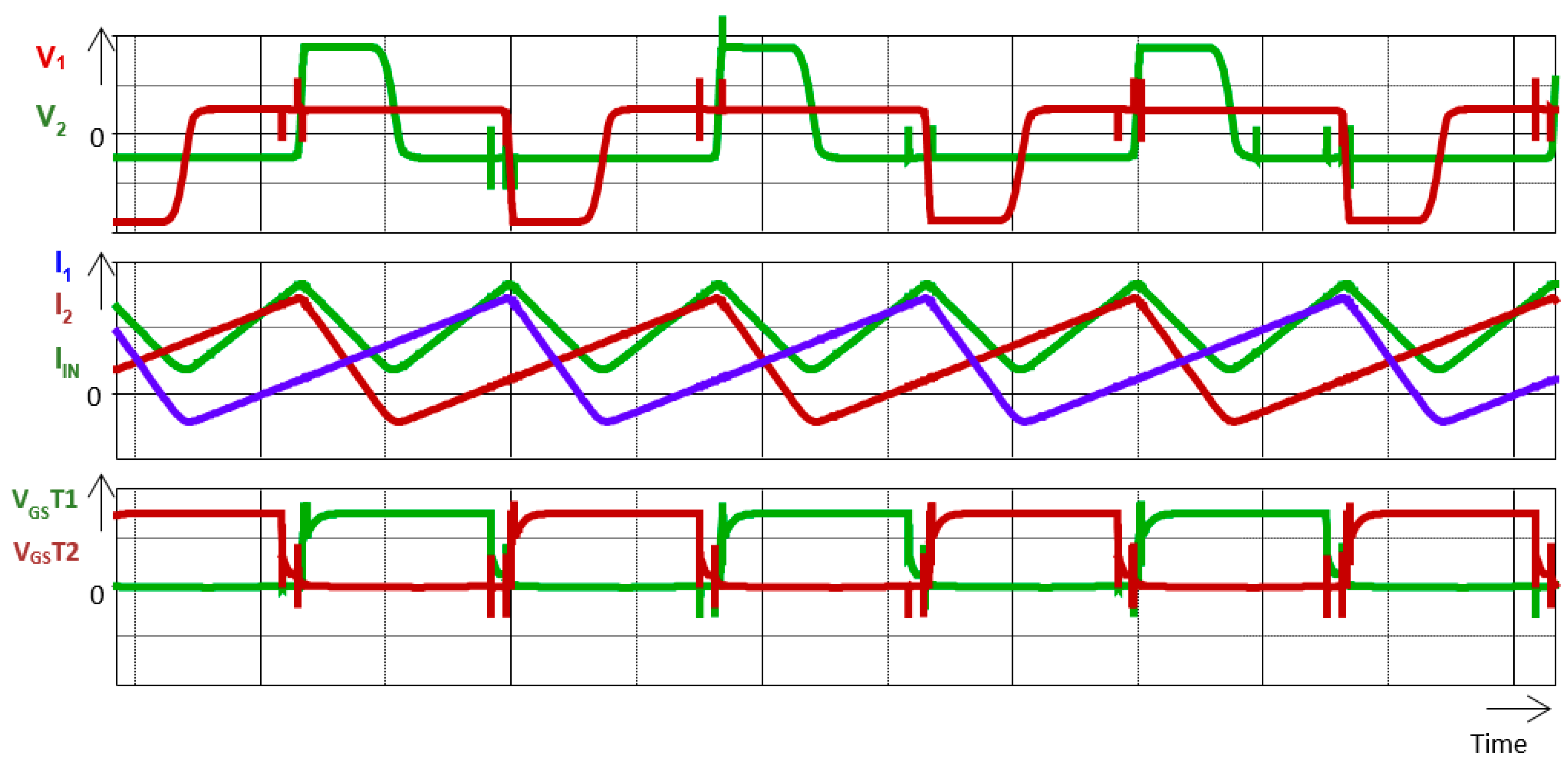
Figure 3.
Proposed dual interleaved boost converter with coupled inductors and demagnetizing circuit.
Figure 3.
Proposed dual interleaved boost converter with coupled inductors and demagnetizing circuit.
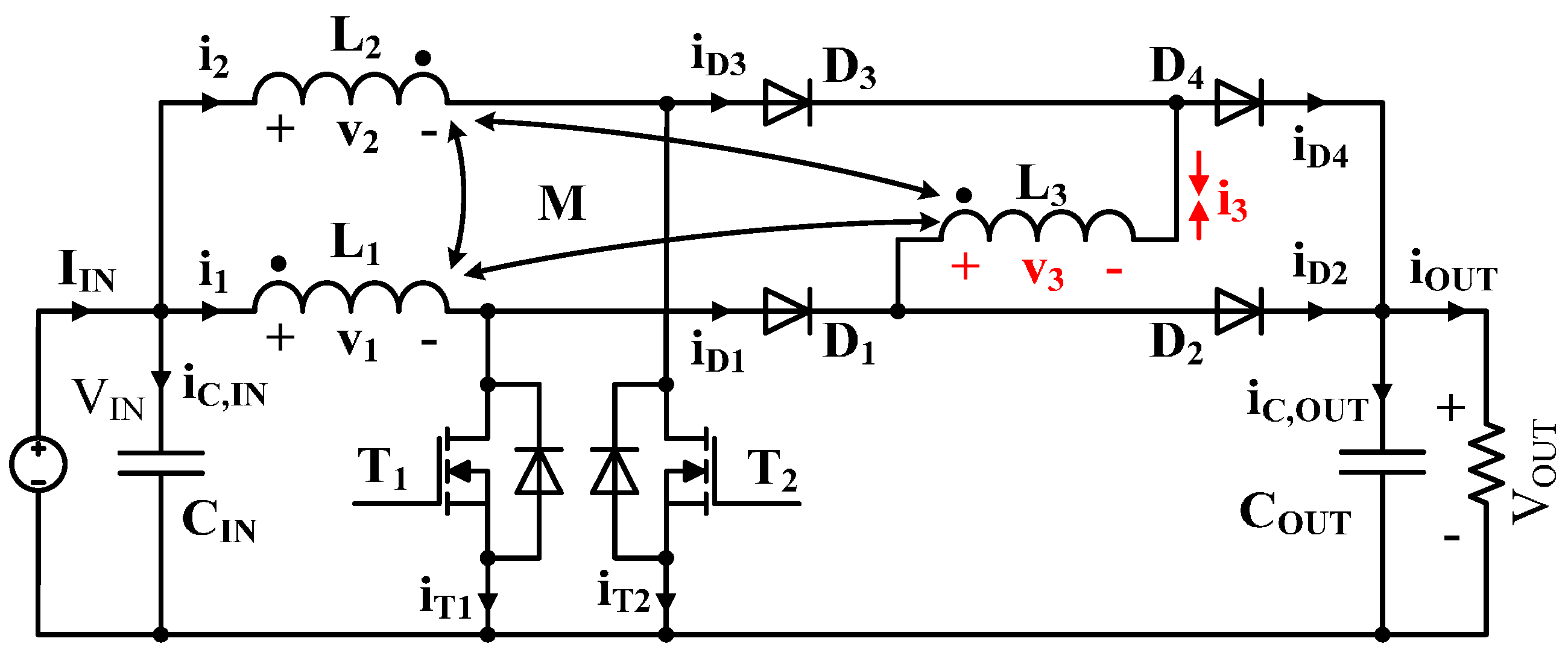
Figure 4.
Driving impulses of transistors T1 and T2.
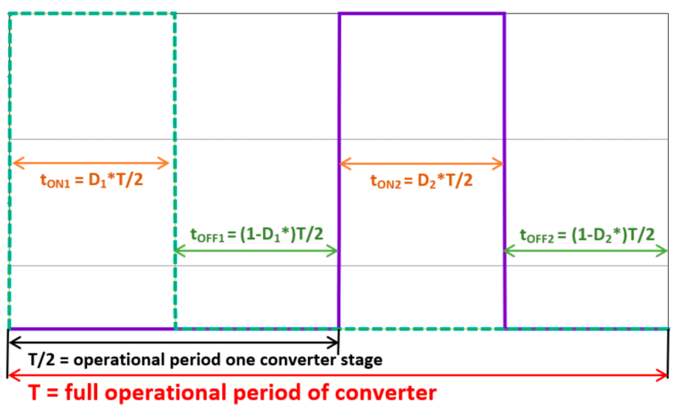
Figure 5.
Operational waveforms for analyzed steady state of proposed converter—nominal load (top: driving signals, middle: voltages on inductors, bottom: inductor currents).
Figure 5.
Operational waveforms for analyzed steady state of proposed converter—nominal load (top: driving signals, middle: voltages on inductors, bottom: inductor currents).
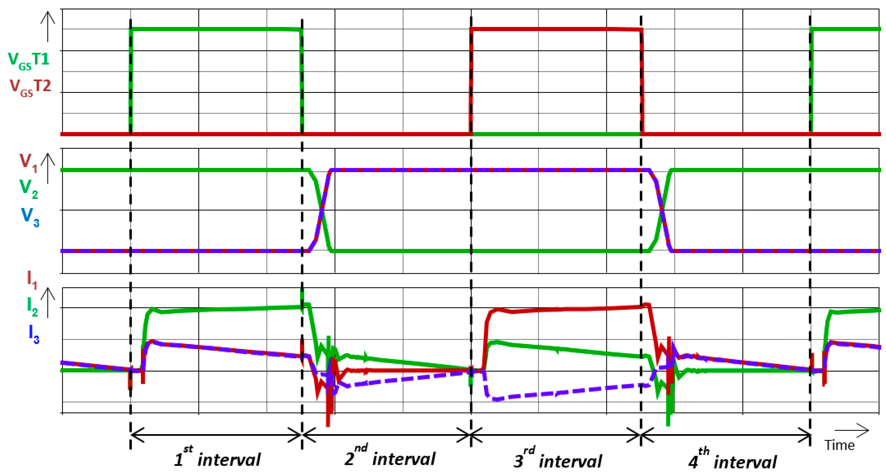
Figure 6.
Equivalent circuit of proposed converter operation during 1st interval.

Figure 7.
Equivalent circuit of proposed converter operation during 2nd interval.

Figure 8.
Equivalent circuit of proposed converter operation during 3rd interval.
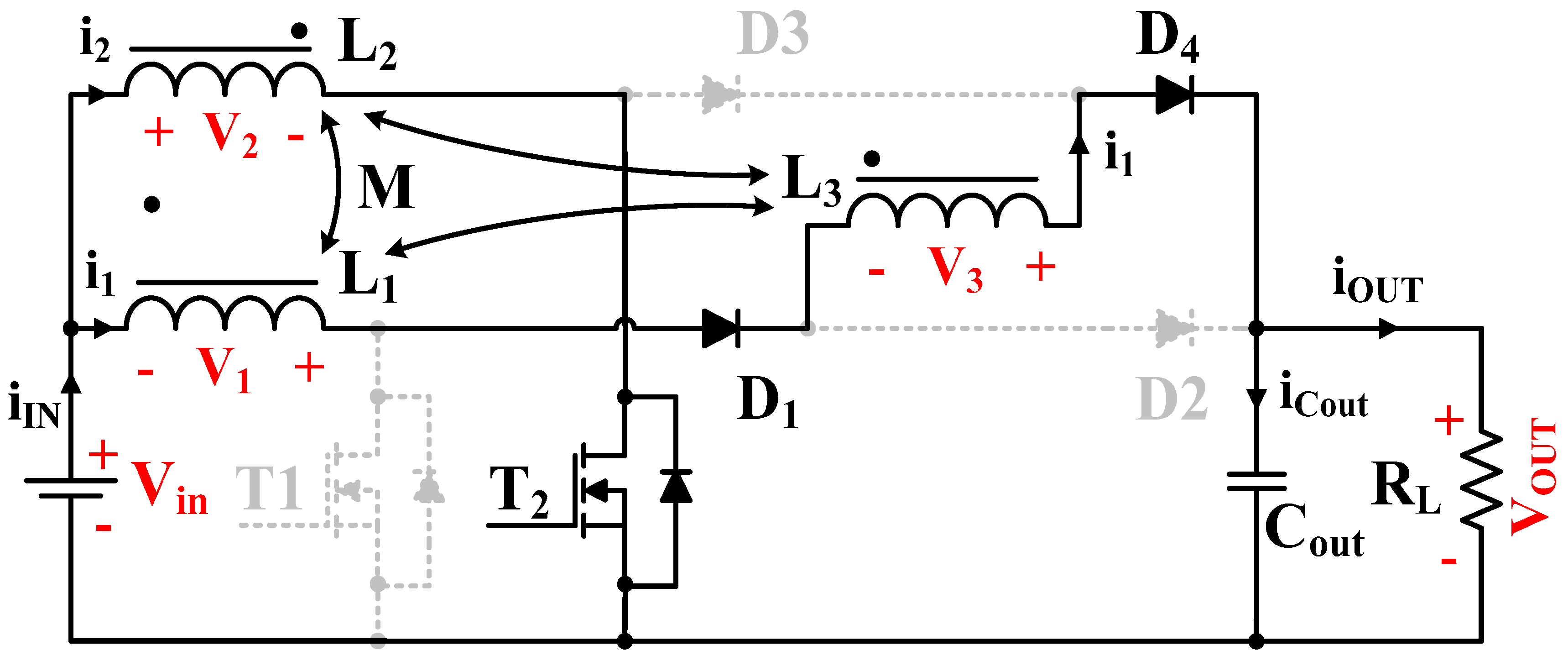
Figure 9.
Equivalent circuit of proposed converter operation during 4th interval.

Figure 10.
Measurement set-up (left) and experimental sample (right) of the proposed converter designed for 1 kW peak of output power.
Figure 10.
Measurement set-up (left) and experimental sample (right) of the proposed converter designed for 1 kW peak of output power.
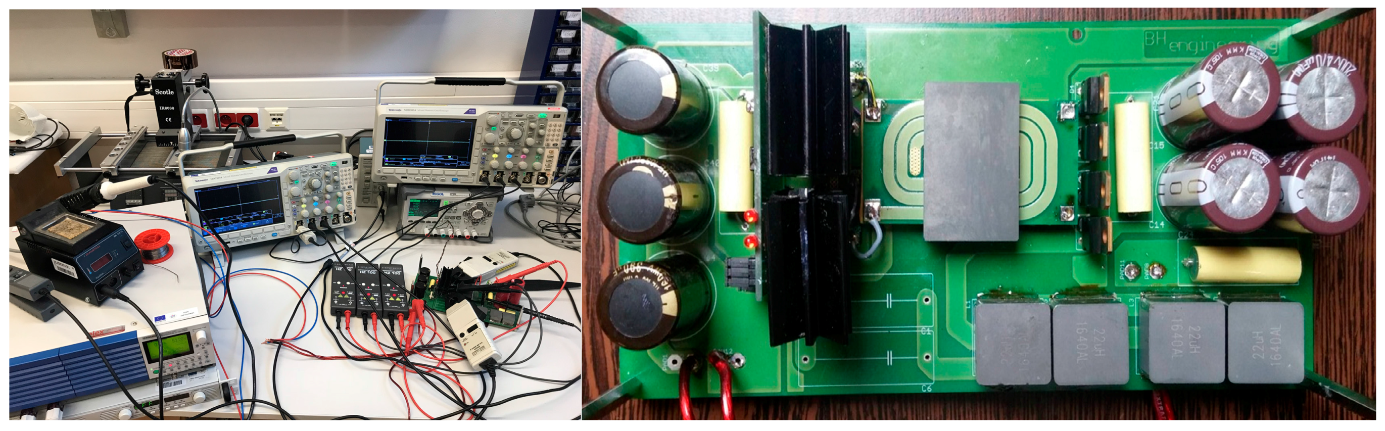
Figure 11.
Current waveforms of the inductors L1–L3 (100% of output power)—Simulation.

Figure 12.
Current waveforms of the inductors L1–L3 (100% of output power)—Measurement.

Figure 13.
Voltage waveforms on the inductors L1–L3 (100% of output power)—Simulation.

Figure 14.
Voltage waveforms on the inductors L1–L3 (100% of output power)—Measurement.

Figure 15.
Voltage and current waveforms of the power transistors T1, T2 (100% of output power)—simulation.
Figure 15.
Voltage and current waveforms of the power transistors T1, T2 (100% of output power)—simulation.
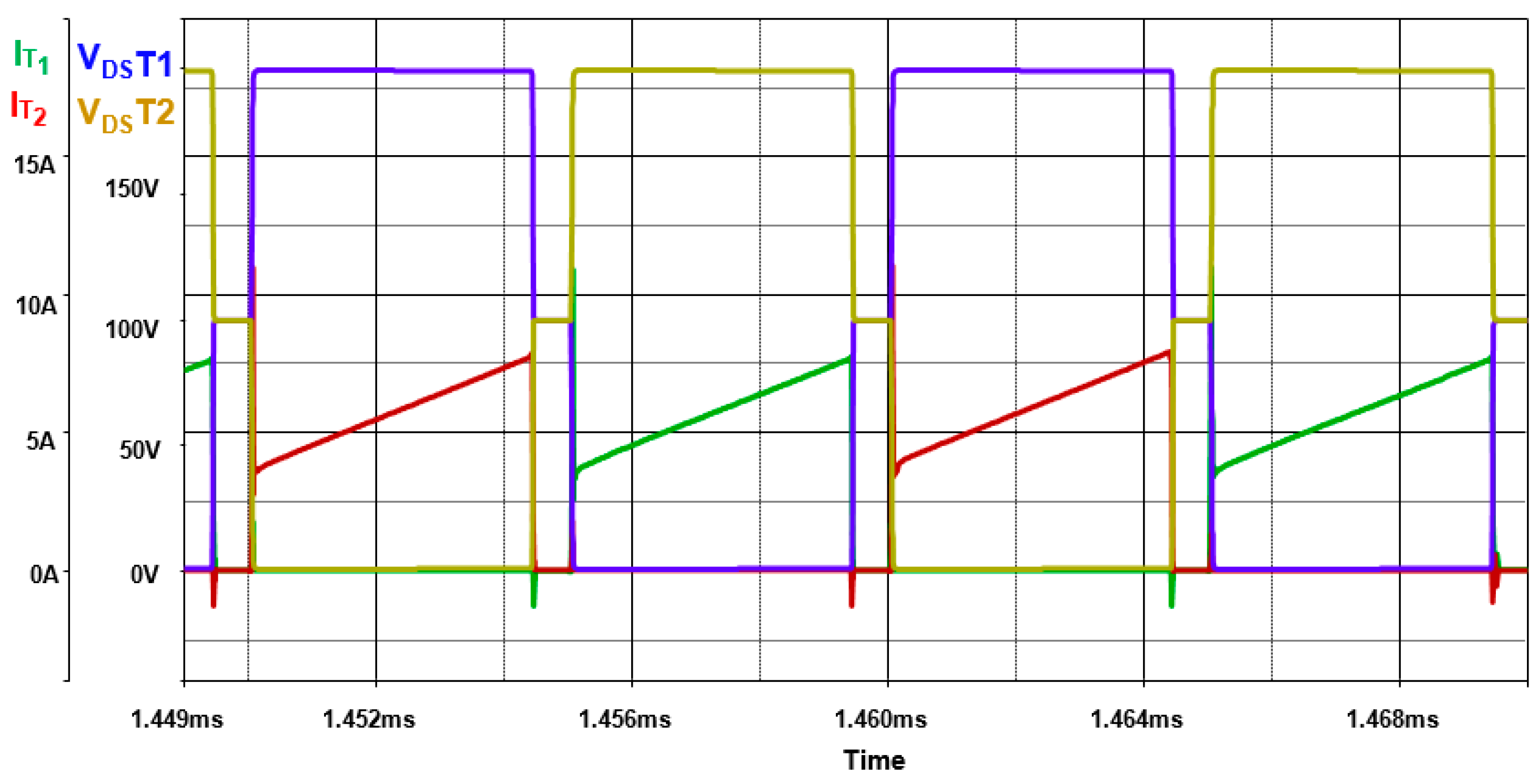
Figure 16.
Voltage and current waveforms of the power transistors T1, T2 (100% of output power)—measurement.
Figure 16.
Voltage and current waveforms of the power transistors T1, T2 (100% of output power)—measurement.

Figure 17.
Voltage and current waveforms of the power diodes D3, D4 (100% of output power)—simulation.
Figure 17.
Voltage and current waveforms of the power diodes D3, D4 (100% of output power)—simulation.

Figure 18.
Voltage and current waveforms of the power diodes D3, D4 (100% of output power)—measurement.
Figure 18.
Voltage and current waveforms of the power diodes D3, D4 (100% of output power)—measurement.

Figure 19.
Dependency of the converter’s efficiency and output voltage on the output power (measurement).
Figure 19.
Dependency of the converter’s efficiency and output voltage on the output power (measurement).
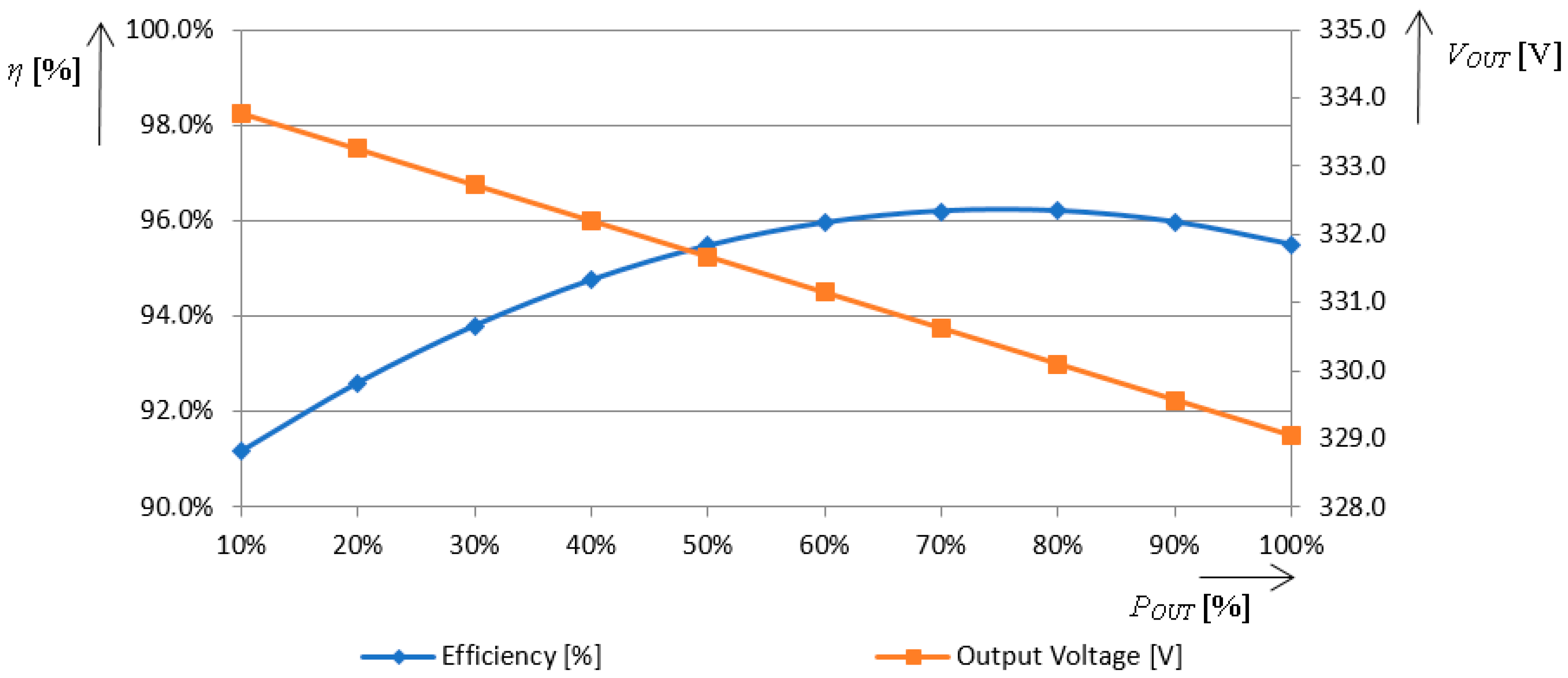
Figure 20.
Power loss distribution of the proposed converter at highest efficiency 96.2%.
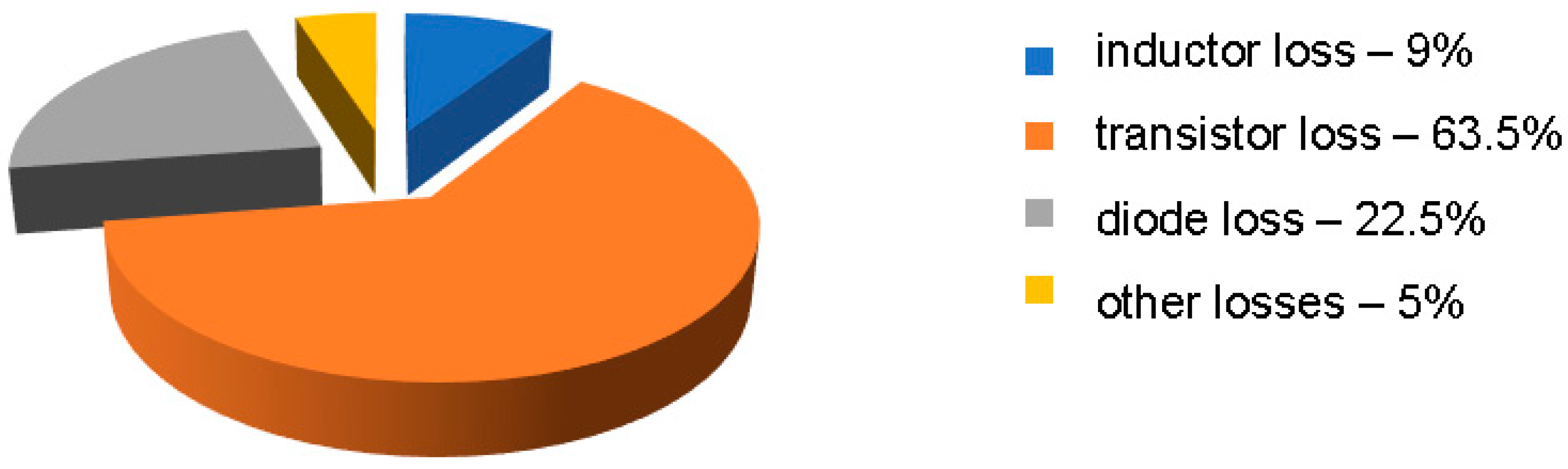
Figure 21.
Dependency of converter’s voltage gain on the duty cycle at POUT = 100% and POUT = 20%.

Figure 22.
Dependency of converter’s voltage gain on the turns ration between L1 = L2 and L3.


Table 1.
Dependency of voltage gain on the inductance ratio.
| Turn’s Ratio (TR) N1 = N2 = NBOOST: AC Inductor N3 | VOUT/VIN (Voltage Gain) |
|---|---|
| 4:1 | 2.2 |
| 3:1 | 2.3 |
| 2:1 | 2.5 |
| 1:1 | 3 |
| 1:2 | 4 |
| 1:3 | 5 |
| 1:4 | 6 |
Table 2.
Values of power losses on the individual components (Computation).
| Component | Power Loss (W) |
|---|---|
| Inductor L1–L3 | 3.71 |
| Transistors | 25.71 |
| Diodes | 9.1 |
| Other—parasitic leads etc. | 2 |
Table 3.
Values of the efficiency and output voltage in dependency on the output power (Measurement).
Table 3.
Values of the efficiency and output voltage in dependency on the output power (Measurement).
| Item | Values | |||||||||
|---|---|---|---|---|---|---|---|---|---|---|
| Output Power (%) | 10 | 20 | 30 | 40 | 50 | 60 | 70 | 80 | 90 | 100 |
| Efficiency (%) | 91.2 | 92.6 | 93.8 | 94.8 | 95.5 | 96.0 | 96.2 | 96.2 | 96.0 | 95.5 |
| Output Voltage (V) | 333.8 | 333.3 | 332.7 | 332.2 | 331.7 | 331.1 | 330.6 | 330.1 | 329.6 | 329.0 |
Table 4.
Values of the converter’s voltage gain in dependency on the duty cycle.
| Duty | 0.05 | 0.1 | 0.15 | 0.2 | 0.25 | 0.3 | 0.35 | 0.4 | 0.45 |
| VOUT/VIN (100% POUT) | 1.54 | 1.86 | 2.14 | 2.4 | 2.66 | 2.93 | 3.22 | 3.5 | 3.8 |
| VOUT/VIN (20% POUT) | 1.63 | 1.99 | 2.29 | 2.56 | 2.81 | 3.07 | 3.32 | 3.58 | 3.86 |
Table 5.
Values of the converter’s voltage gain in dependency on the turns ration between boost and reset inductors (N1 = N2 = constant, N3 = <1–11>).
Table 5.
Values of the converter’s voltage gain in dependency on the turns ration between boost and reset inductors (N1 = N2 = constant, N3 = <1–11>).
| Turns ratio N3/N1 | 0.17 | 0.33 | 0.50 | 0.67 | 0.83 | 1.00 | 1.17 | 1.33 | 1.50 | 1.67 | 1.83 |
| Number of turns N1 = N2 | 6 | 6 | 6 | 6 | 6 | 6 | 6 | 6 | 6 | 6 | 6 |
| Number of turns N3 | 1 | 2 | 3 | 4 | 5 | 6 | 7 | 8 | 9 | 10 | 11 |
| Voltage gain VOUT/VIN | 2.06 | 2.16 | 2.26 | 2.36 | 2.45 | 2.94 | 3.1 | 3.25 | 3.41 | 3.56 | 3.71 |
Table 6.
Values of the converter’s voltage gain in dependency on the turns ration between boost and reset inductors (N1 = N2 = constant, N3 = <12–48>).
Table 6.
Values of the converter’s voltage gain in dependency on the turns ration between boost and reset inductors (N1 = N2 = constant, N3 = <12–48>).
| Turns ratio N3/N1 | 2.00 | 2.17 | 2.33 | 2.50 | 3.00 | 4.00 | 5.00 | 6.00 | 7.00 | 8.00 |
| Number of turns N1 = N2 | 6 | 6 | 6 | 6 | 6 | 6 | 6 | 6 | 6 | 6 |
| Number of turns N3 | 12 | 13 | 14 | 15 | 18 | 24 | 30 | 36 | 42 | 48 |
| Voltage gain VOUT/VIN | 3.86 | 4.01 | 4.16 | 4.3 | 4.72 | 5.51 | 6.21 | 6.82 | 7.35 | 7.76 |
Table 7.
Comparisons of proposed converter to other circuit alternatives.
| Characteristic/Parameter | Proposed Converter | Dual Interleaved Boost Converter | Boost Converter |
|---|---|---|---|
| Output power | 1 kW | 1 kW | 1 kW |
| Output voltage ripple | 19 mV | 180 mV | 364 mV |
| Input ripple current | 8.8 A | 34 A | 28 A |
| Output capacitor | 33 µF | 470 µF | 470 µF |
| Inductor Volumes | EI PLT 43/10 | E50/27/15 | ETD59 |
| Efficiency (full power) | 95.5% | 91% | 90% |
| Voltage gain (VIN/VOUT) | 1:8 | 1:19 | 1:10 |
© 2018 by the authors. Licensee MDPI, Basel, Switzerland. This article is an open access article distributed under the terms and conditions of the Creative Commons Attribution (CC BY) license (http://creativecommons.org/licenses/by/4.0/).
Share and Cite
MDPI and ACS Style
Frivaldsky, M.; Hanko, B.; Prazenica, M.; Morgos, J. High Gain Boost Interleaved Converters with Coupled Inductors and with Demagnetizing Circuits. Energies 2018, 11, 130. https://doi.org/10.3390/en11010130
AMA Style
Frivaldsky M, Hanko B, Prazenica M, Morgos J. High Gain Boost Interleaved Converters with Coupled Inductors and with Demagnetizing Circuits. Energies. 2018; 11(1):130. https://doi.org/10.3390/en11010130
Chicago/Turabian StyleFrivaldsky, Michal, Branislav Hanko, Michal Prazenica, and Jan Morgos. 2018. "High Gain Boost Interleaved Converters with Coupled Inductors and with Demagnetizing Circuits" Energies 11, no. 1: 130. https://doi.org/10.3390/en11010130
Note that from the first issue of 2016, this journal uses article numbers instead of page numbers. See further details here.