A New ZVS Tuning Method for Double-Sided LCC Compensated Wireless Power Transfer System


Faculty of Electric Power Engineering, Kunming University of Science of Technology, Kunming 650500, China
*
Author to whom correspondence should be addressed.
Energies 2018, 11(2), 307; https://doi.org/10.3390/en11020307
Submission received: 31 December 2017
/
Revised: 19 January 2018
/
Accepted: 22 January 2018
/
Published: 1 February 2018
(This article belongs to the Special Issue Wireless Power Transfer and Energy Harvesting Technologies)
Abstract
:This paper presents a new zero voltage switching (ZVS) tuning method for the double-sided inductor/capacitor/capacitor (LCC) compensated wireless power transfer (WPT) system. An additional capacitor is added in the secondary side of the double-sided LCC compensation network in order to tune the network to realize ZVS operation for the primary-side switches. With the proposed tuning method, the turn off current of the primary-side switches at the low input voltage range can be reduced compared with the previous ZVS tuning method. Consequently, the efficiency of the WPT at the low input voltage range is improved. Moreover, the relationship between the input voltage and the output power is more linear than that of the previous ZVS tuning method. In addition, the proposed method has a lower start-up voltage. The analysis and validity of the proposed tuning method are verified by simulation and experimental results. A WPT system with up to 3.5 kW output power is built, and 95.9% overall peak efficiency is achieved.
1. Introduction
Wireless power transfer (WPT) technology can deliver electric power over certain distances without metal-to-metal contact by utilizing energy-contained fields [1,2]. WPT has attracted more and more research interest due to its convenience, safety and other advantages [3], particularly in electric vehicle (EV) charging [4,5].
Many academic papers have been published on WPT and many aspects of WPT have been studied in order to improve the performance of the WPT [4]. Among them, the compensation circuit is essential because it can be used to tune the resonant frequency of the system, reduce the reactive power in the power electronics converter, and improve the transferred power capability and efficiency [4,6]. According to the way in which the compensation capacitors are connected to the primary and secondary coils in the compensation networks, the basic compensation topologies can be classified into four types, that is, series–series (SS), series–parallel (SP), parallel–series (PS) and parallel–parallel (PP) [6,7]. A detailed analysis of these four basic compensation topologies has been conducted in [8,9]. It was concluded in [9] that SS and SP are superior to the other two compensation topologies. However, the SP compensation circuit is easily mistuned because the primary compensated capacitance relates to the coupling coefficient [10], which means the resonant frequency is dependent on the coupling coefficient. Therefore, SS compensation topology is superior to the other three compensation topologies because its resonant frequency is independent of the coupling coefficient and the load conditions [6]. The defect of the SS compensation topology is the poor output voltage regulation capability [11], so many other compensation topologies have been proposed in order to improve the efficiency or realize other purposes [12]. In [13], an inductor/capacitor (LC) compensation network is employed for the primary side and an inductor/capacitor/inductor (LCL) resonant network is formed for WPT. However, the resonant frequency of this compensation topology is dependent on the coupling coefficient and the load conditions [6]. In [14], LC compensation networks are employed for both the primary side and the secondary side and a bidirectional power transfer is achieved. In [15], an inductor/capacitor/inductor T-type (LCL-T) resonant converter is proposed which can be treated as a current source. Its primary side current is only determined by the input voltage, so the primary side current can be easily controlled. In [16], an LCC compensation network is adopted for the primary side and a zero current switching (ZCS) is achieved by tuning the parameters of the compensation network. In [17], the LCC compensation network is applied for the secondary side, which can minimize the reactive power at the secondary side and achieve a unit power factor pickup. A double-sided LCC compensation network is proposed for the WPT in [18]. Its resonant frequency is irrelevant to the coupling coefficient and the load conditions. Meanwhile, its tuning method for realizing zero voltage switching (ZVS) is also presented in [18]. A comparison study on SS and double-sided LCC compensation topology is carried out in [6]. It is concluded that double-sided LCC compensation topology is less sensitive to the self-inductance variations, lower voltage and current stress and higher efficiency compared with the SS compensation topology. Integrated LCC compensation topologies are proposed in [10,19] in order to reduce the coil size and make the system more compact with high efficiency. In [19], a numerical method to tune the compensation network parameters for ZVS is also presented. However, the turn off currents of the primary side switches are relatively large at the low input voltage condition which lowers the efficiency of the system [18,19]. In addition, the relationship between the input voltage and the output power is not so linear in the WPT system using the ZVS tuning method proposed by [18].
For high voltage high frequency metallic oxide semiconductor field effect transistor (MOSFET) switching applications, the zero voltage turn on soft switching (ZVS) condition is very important due to the poor reverse recovery characteristics of the MOSFET’s body diode [20]. At the ZVS condition, the turn on switching loss is almost zero and the turn off loss is proportional to the turn off current [21]. In most of the WPT studies, the system is simply tuned to the inductive region to realize ZVS [22,23]. The turn off currents are not accurately designed. It is important to optimize the turn off current while maintaining the ZVS condition to minimize the switching loss.
In this paper, a new ZVS tuning method for double-sided LCC-compensated WPT system is proposed. For the secondary side, an additional capacitor is added to the compensation topology in order to realize ZVS operation of the primary side switches. With the proposed ZVS tuning method, the resonant frequency of the resonant network is still irrelevant with the coupling coefficient and the load conditions. Meanwhile, the turn off current of the primary-side switches at the low input voltage range can be reduced. Consequently, the efficiency of the WPT at the low input voltage range is improved. Moreover, the relationship between the input voltage and the output power is more linear than that of the previous ZVS tuning method. The proposed new ZVS tuning method and the parameter design method are also analyzed and presented in this paper, respectively. Simulation and experimental results verify the analysis and validity of the proposed circuit and the tuning method. A WPT system with up to 3.5 kW output power and 95.9% peak efficiency is built to verify the proposed ZVS tuning method.
The remainder of this paper is organized as follows. The basic circuit structure of the double-sided LCC compensation network and the new tuning method for ZVS operation are presented in Section 2. The parameter design of the proposed new ZVS tuning method is presented in Section 3. Simulated and experimental results are presented in Section 4. The conclusions are drawn in Section 5.
2. Double-Sided LCC Compensation Network and Parameter Tuning for ZVS
2.1. Double-Sided LCC Compensation Network
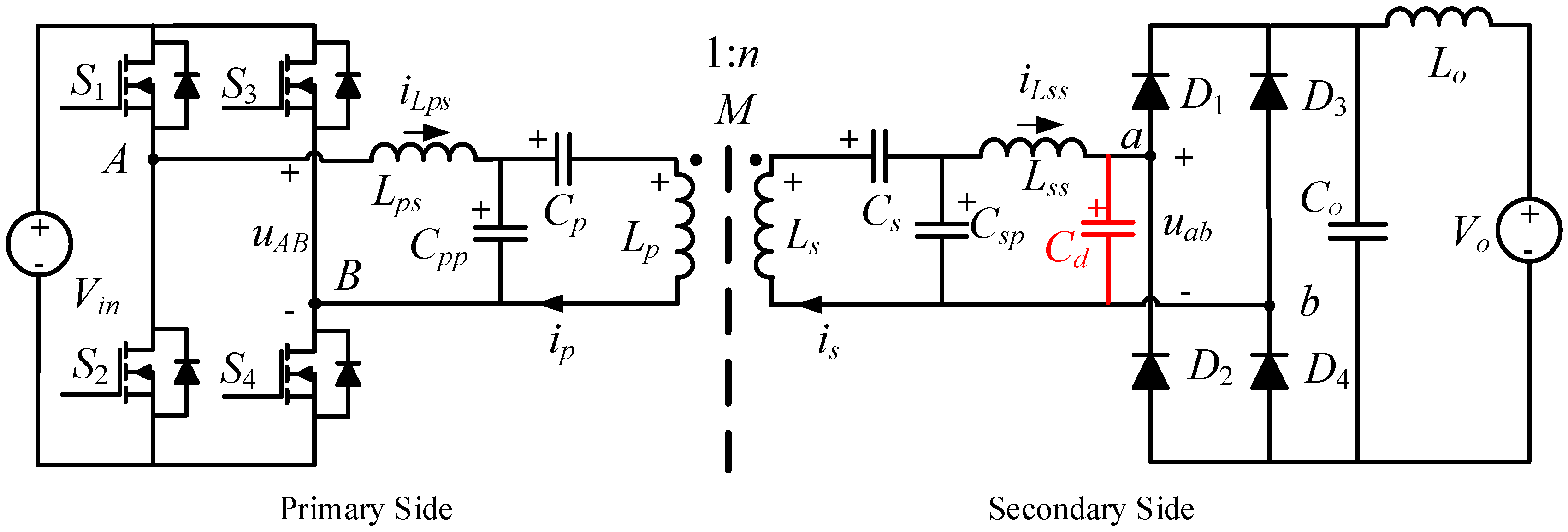
Figure 1 shows the double-sided LCC compensation network and corresponding power electronics circuit components. S1–S4 are the primary side MOSFEs. Lps, Cpp and Cp form the primary side compensation network. Lp is the self-inductance of the transmitting coils. M is the mutual inductance of the transmitting coil and the receiving coil. Ls represent the self-inductance of the transmitting coils. Lss, Csp and Cs form the secondary side compensation network. Cd is a capacitor added in order to achieve ZVS for the primary side metallic oxide semiconductor field effect transistors (MOSFEs). D1–D4 represent the secondary side rectifier diodes. uAB is the input voltage of the primary side compensation network, which is the voltage generated by Vin and the switching MOSFET S1–S4. uab represents the output voltage of the secondary side compensation network, which is related to the output voltage Vo. The currents on Lp, Ls, Lps and Lss are represented by ip, is, iLps, iLss as shown in the Figure 1.
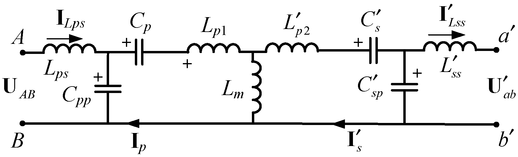
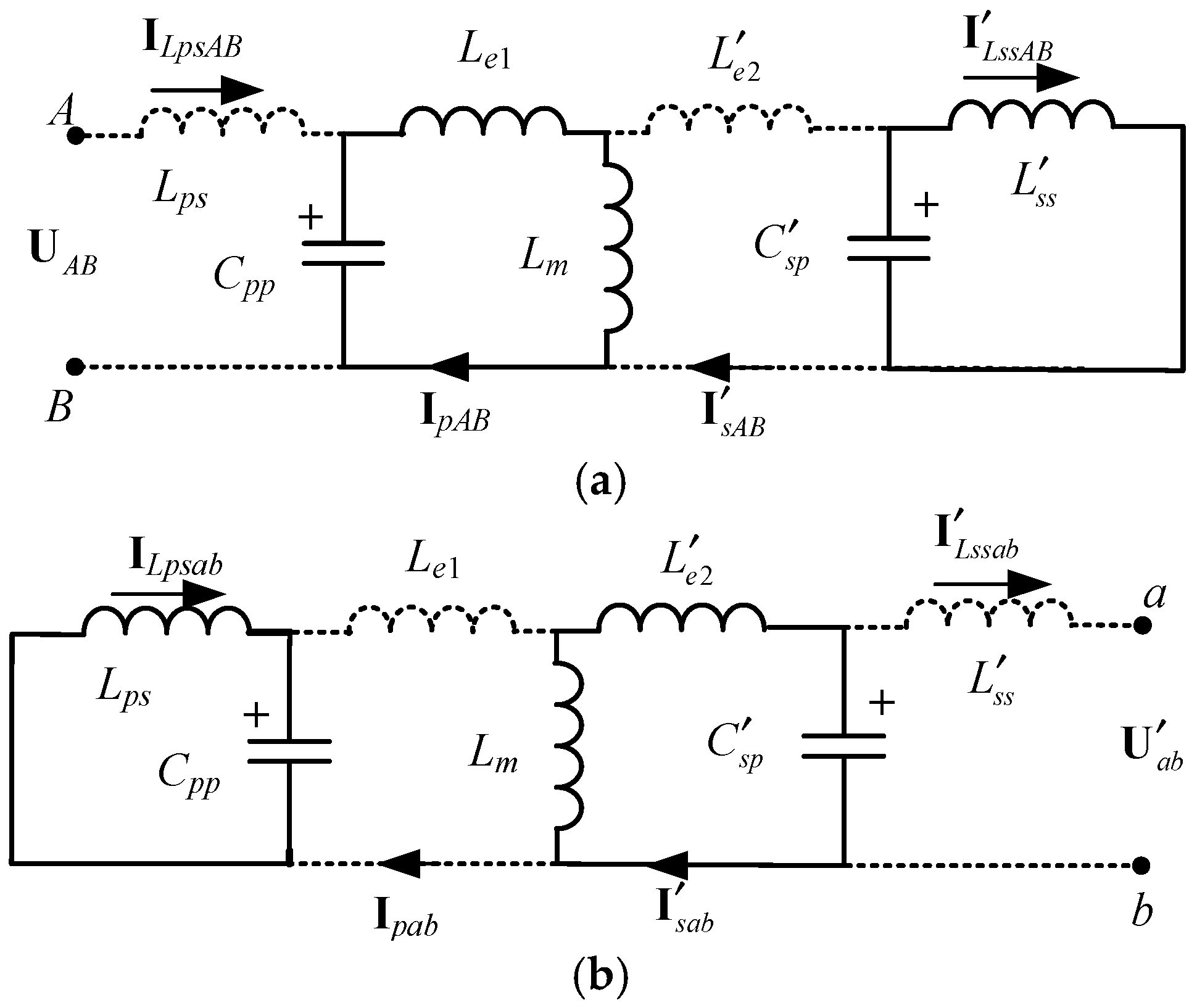
According to [18], the equivalent circuit to the circuit in Figure 1 referring to the primary side can be derived as shown in Figure 2; the circuit status at resonant frequency can be derived as shown in Figure 3. In Figure 2 and Figure 3, UAB, Uab, IP, IS, ILps, ILss represent the phasor form of the corresponding variables.
The variables in Figure 2 can be expressed by the following equations
where k is the coupling coefficient between the transmitting and receiving coils, UAB represent the root mean square value of UAB.
The variables and in Figure 3 can be expressed by the following equations
For Equations (1) and (2), the influence of Cd is implied in . The relation between Cd and will be analyzed in the next section. It can be seen from Figure 2 and Figure 3 that the added Cd has no impact on the equivalent circuit of the double-sided LCC compensation network which is presented in [18]. Therefore, the similar analysis process presented in [18] can be used in this paper. However, the added Cd has impacts on , so the waveform of in Figure 3 is different from the waveform of in [18]. Moreover, the parameter tuning method for ZVS operation is also different.
2.2. Parameter Tuning for ZVS
For the MOSFETs, the turn off switching loss is much smaller than its turn on loss at hard switching [20]. Therefore, it is better that all the MOSFETs are turned on at ZVS conditions in order to reduce the overall switching loss. To realize ZVS for a MOSFET, the MOSFET should be turned on when the body diode is conducting. This means the resonant current of the primary side should lag the resonant voltage in order to form the ZVS operation condition for all MOSFETs. The added Cd in the secondary side of the compensation network should be properly designed in order to achieve the ZVS operation.
According to the Figure 3a,b, the following equations can be derived by superposition principle
where the subscript ‘1st’ represents the first harmonic component of the corresponding item.
According to Equation (3), ILss_1st leads UAB by a phase ϕ1, which can be expressed as
To achieve ZVS conditions at a small turn off current, the analysis accuracy of the turn off current is very important. Therefore, the high order harmonics of the square voltage cannot be neglected. The effect of the high order harmonics current is shown in Figure 4. The phase between uab zero crossing time tb and its maximum value time tc is represented by a. The phase between the zero crossing of iLss and uab is represented by ϕab. Meanwhile, iLss contains not only the first order current but also the high order harmonic currents. The interaction of the high order harmonics between the primary and secondary side can be neglected because the compensation networks form a high order filter between the primary side and the secondary side. Moreover, a is close to zero as shown in Figure 4, so the waveform of uab is firstly approximated by a square wave. Therefore, the high order harmonic currents of the Lss can be roughly expressed as:
In the time domain, the high order harmonic currents of the Lss can be expressed as
Solve the Equation (8), then the following equation can be derived
According to Equation (6), leads by a phase which equals to 90°. So reaches the peak when jumps at the time tb. The peak value of the can be calculated by
According to Equations (8)–(10), the high order harmonics can be approximated by
where is the peak value of the total high order current.
Assuming tb = 0, ta = , then the following equations can be derived:
Integrating the left side of Equation (13), then the following equation can be derived:
where Vo is the output voltage.
Solving the Equation (16), then the phase shift ϕab can be expressed as
According to Figure 4, the following equation can be derived:
However, the effect of the added Cd on the magnitude of hp should be taken into consideration in order to calculate ϕ2 accurately. According to Figure 4, the charge time from tb to tc is around 0.4 times of the charge time from ta to tb, so the following equations can be derived:
where is the modified peak value of the total high order current.
Substituting Equation (20) into (17), then the following equations can be derived:
Finally, the phase by which leads can be obtained:
In Figure 4, ILss_1st leads Uab by a phase ϕ2. According to Equation (5), the following equations can be derived:
According to [18], the total high order current peak value of the primary side can be calculated by:
The turn off current of the MOSFET is determined by both the first order and the high order harmonic currents. According to Equations (26) and (27), the turn off current of the MOSFET can be calculated as:
According to the MOSFET parameters, a minimum turn off current IOFF_min which can achieve ZVS can be determined [21]. Then,
According to Equations (21), (24) and (28), it can be seen that a turn off current can be calculated for a given Cd. When the value of Cd is increased, the phase shift ϕab and ϕ2 will also be increased. Consequently, the turn off current will also be increased.
3. Parameter Design
In this section, a 3.6 kW WPT system is designed according to the above analysis. The parameters of the WPT system are shown in Table 1.
If UAB is not too low, Figure 4 and Equations (7)–(9) satisfies. Thus ϕ2 < ϕ0/2 ≈ 0.2, and cosϕ2 ≈ 1. From Table 1 and according to the design principle for minimizing the total reactive power in Lp and Ls [24], the Lps and Lss can be designed as
The values of Cpp and Csp can be derived from the following equations,
The values of Cps and Css can also be calculated from
The minimum turn off current is different for different MOSFET and dead-time settings. The turn off current should be large enough to discharge the junction capacitors within the dead-time in order to achieve ZVS, which can be expressed as [21]:
where is the maximum input voltage, uds is the drain-source voltage of the MOSFET, is the junction capacitance which is a function of uds, and is the dead-time. In this paper, Cree C3M0065090D SiC MOSFET (Cree, Research Triangle Park, NC, USA) is chosen as the primary side switches. According to the MOSFET parameters from the datasheet and Equation (34), the turn off current should be larger than 1A in order to realize ZVS. Therefore, the minimum turn off current IOFF_min is designed to be 2A.
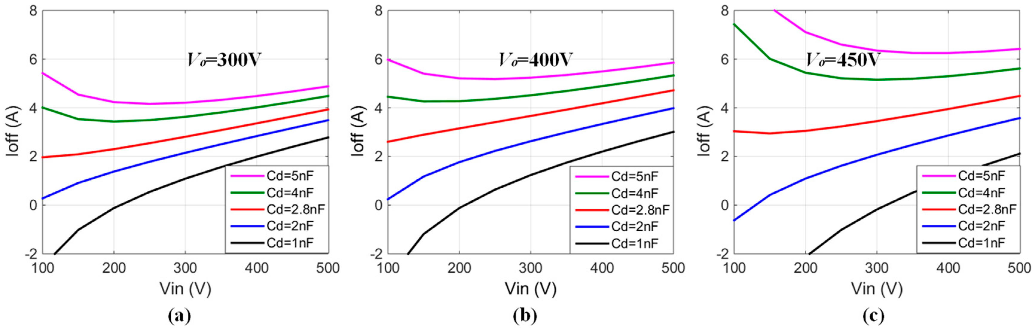
Theoretical results of the MOSFETs’ turn off current IOFF with different values of Cd are shown in Figure 5. For a given Cd, the turn off current varies as the input voltage increasing. Therefore, the selection of Cd should satisfy the minimal turn off current requirement for all the input voltage. It can be seen from the Figure 5a that the value of Cd can be designed to be 2.8 nF in order to ensure that the turn off current is larger than 2A.
According to the above calculations, the designed parameters of the compensation network is shown in Table 2.
4. Simulation and Experimental Results
4.1. Simulated Results
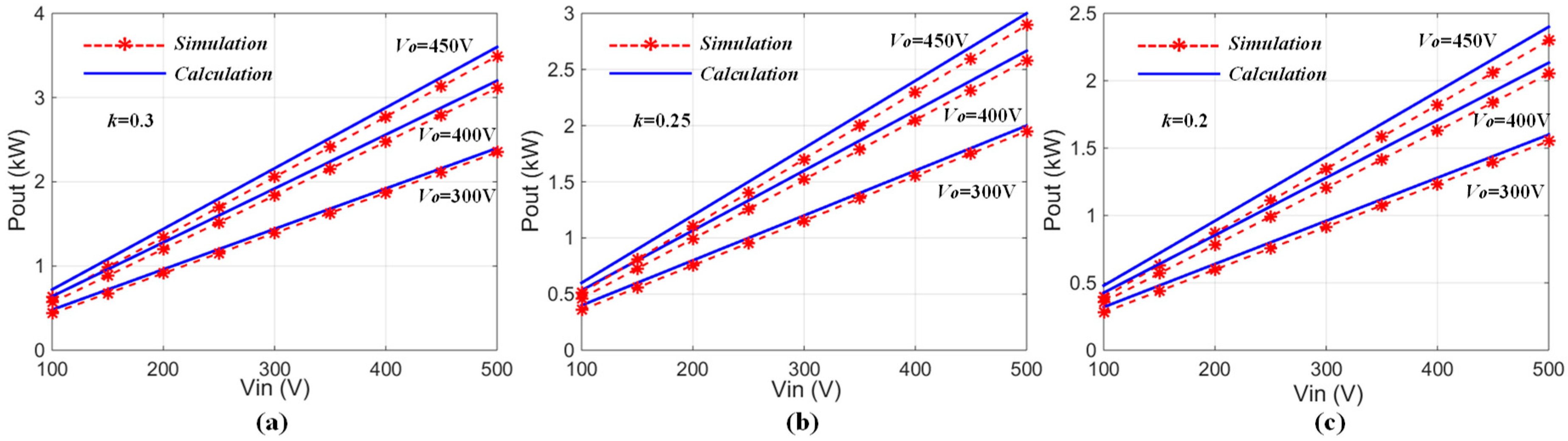
To evaluate the performance of the proposed ZVS tuning method, a simulation model is built in LTspice. The parameters of the simulation model are shown in Table 1 and Table 2. The various misalignments between transmitting coil and the receiving coil can be reflected by the different coupling coefficients. Therefore, three coupling coefficients, namely, k = 0.2, 0.25, 0.3, and three output voltages, Vo = 300, 400, and 450 V, are chosen as case studies in the simulations. Figure 6 shows the comparison of simulation and theoretical calculation results for the output power as a function of input voltage for three coupling coefficients and three output voltage. It can be seen from the Figure 6 that the simulation results agree well with the theoretical analysis and the output power varies linearly with the input voltage from 100 V to 500 V.
Figure 7 shows the comparison of simulation and theoretical calculation results for the turn off currents as a function of input voltage for three coupling coefficients and three output voltages. It can be seen from the Figure 7 that the simulation results agree well with the theoretical analysis, which verifies the validity of the theoretical analysis.
4.2. Experimental Results
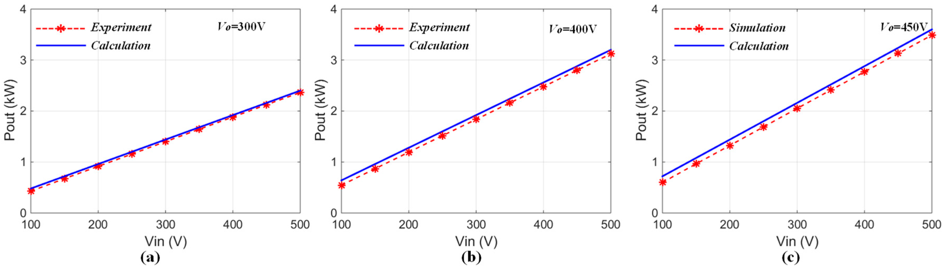
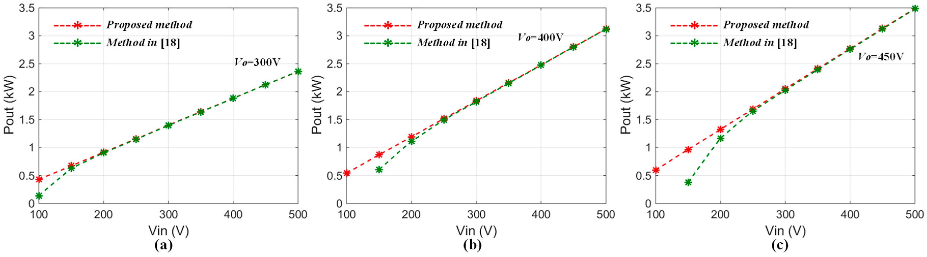
A WPT experimental setup was built as shown in Figure 8a in order to verify the theoretical analysis and simulation results. The parameters of the prototype are tabulated in Table 1 and Table 2. The widths of the transmitter coil and the receiver coil are 500 mm and 450 mm, respectively. The air gap between two coils is 120 mm. The coupling coefficient k = 0.3, and three output voltages, Vo = 300, 400, and 450 V, are chosen as the case studies in the experiment. An electronic load at constant voltage mode is used to represent the battery pack for flexible voltage adjustment. The efficiency screen shot from power meter WT1800 (Yokogawa, Tokyo, Japan) at output power of 3.5 kW is shown in Figure 8b. Urms1, Irms1 and Urms5, Irms5 represent the voltages and currents of the input side and the output side, respectively. P1 and P5 represent the input and output power, respectively. is the efficiency of the WPT system. Figure 9 shows comparison of theoretical and experimental output power as a function of input voltage for three output voltages. The experimental output power matches well with the theoretical calculation. They vary linearly with the input voltage very well even at the low input voltage. The comparison of the experimental output power of the proposed new ZVS tuning method and the previous method proposed in [18] are shown in Figure 10. The relationship between the input voltage and the output power of the proposed new ZVS tuning method is more linear than that of the previous ZVS tuning method, especially at the low input voltage conditions. Moreover, the WPT system using the previous ZVS tuning method cannot start up at Vin = 100 V when Vo = 400 and Vo = 450 V. This is why the output power data of the WPT system using the previous ZVS tuning method are not shown at Vin = 100 V in Figure 10b,c. It is obvious that the proposed new ZVS tuning method has a lower start-up voltage.
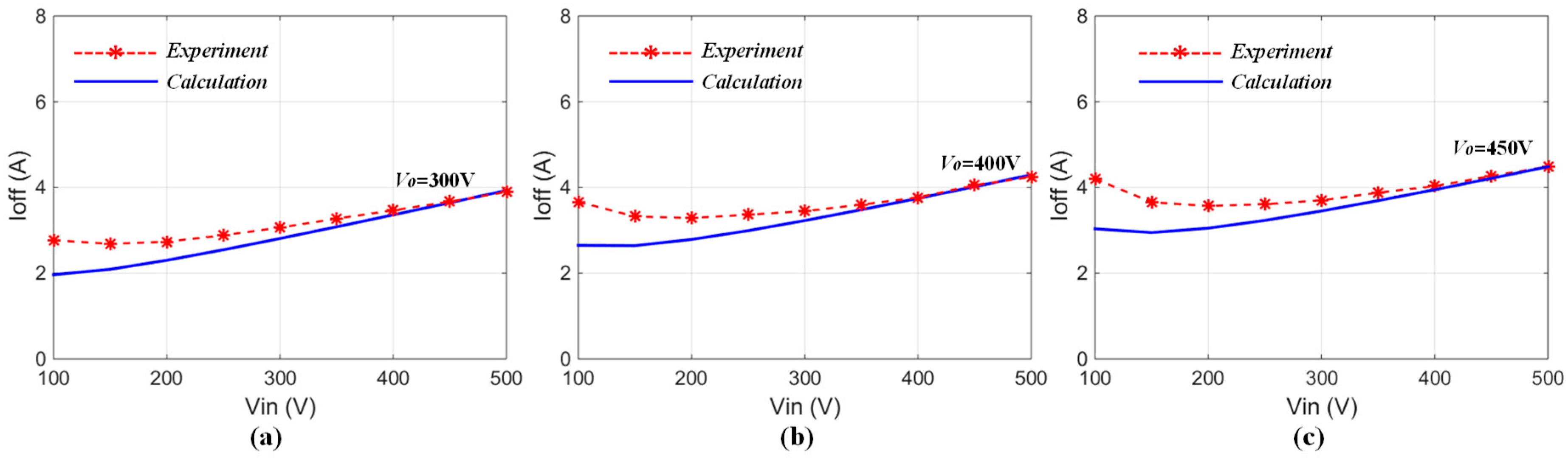
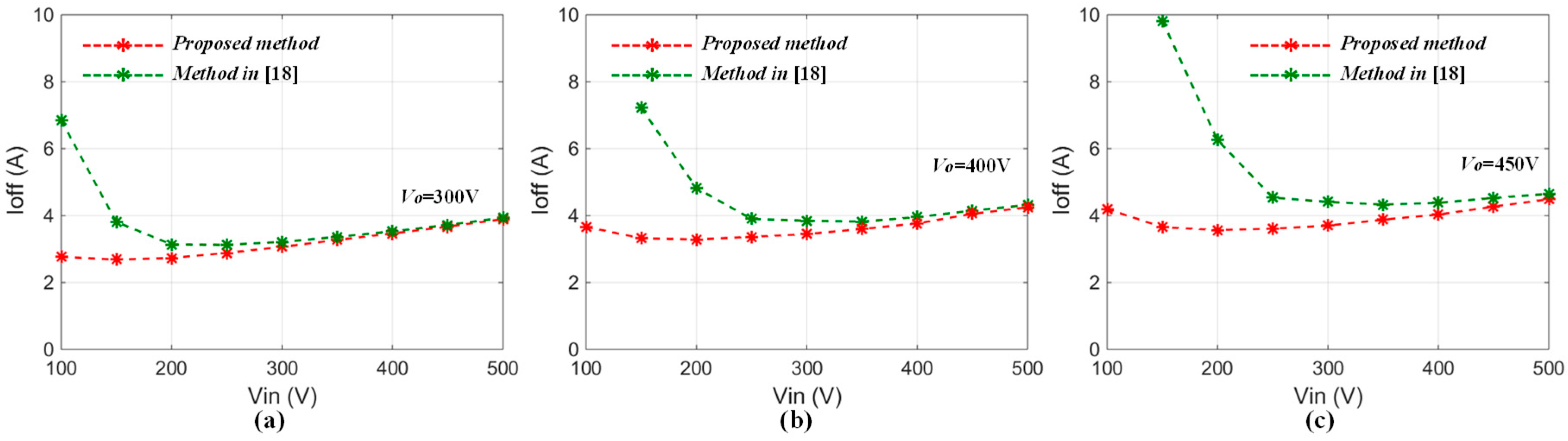
Figure 11 shows the theoretical calculation and experimental results of MOSFETs’ turn off currents for different output voltages. The experimental results agree well with the theoretical analysis. The primary-side waveforms are shown in Figure 12 when the WPT system steadily delivers 3.5 kW to the load. At this operating point, the input voltage equals to 500 V, while the output voltage equals to 450 V. The turn off current of the MOSFET IOFF equals 4.5 A and a good ZVS condition is achieved. Although the turn off current is higher than required, it is quite small compared with the peak current. The comparison of MOSFETs turn off currents for the proposed new ZVS tuning method and the previous ZVS tuning method is shown in Figure 13. It can be seen that the MOSFETs turn off currents of the proposed new ZVS tuning method are smaller those that of the previous ZVS tuning method, especially at the low input voltage conditions.
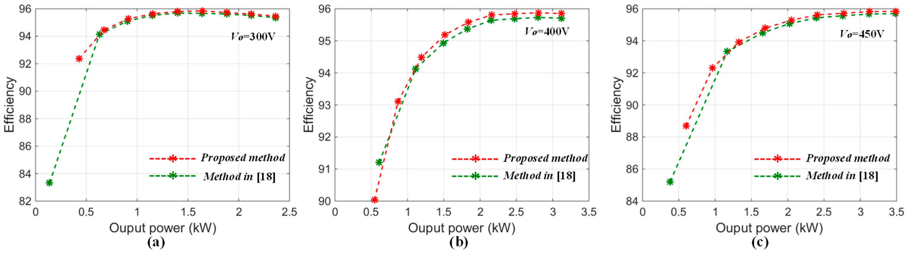
Figure 14 shows the comparison of the experimental efficiencies from the direct current (DC) power source to the battery load for the proposed new ZVS tuning method and the previous ZVS tuning method. In the experiment, an electronic load at constant voltage mode is employed to take the position of a real battery pack in order to facilitate voltage adjustment. A power meter WT1800 from Yokogawa is used to measure the efficiency of the WPT system. The maximum measured efficiency of the proposed new ZVS tuning method is 95.9% when Vin = 450 V, Vo = 400 V, as shown in Figure 14b. At this point, an efficiency improvement of about 0.15% is achieved compared with the previous ZVS tuning method. For the low output power range, the efficiency of these two ZVS tuning methods are almost the same when Vo = 400 V, while a significant efficiency improvement can be achieved by using the proposed new ZVS method when Vo = 300 V and Vo = 450 V. For the high output power range (>1.5 kW), the proposed new ZVS tuning method has a little higher efficiency for all the output voltages.
Besides the efficiency and better operations at low input voltage, the proposed method by employing Cd provides an easier, more flexible way to optimize the turn-off current. In the previous method, the resonant capacitor C2 needs to be tuned. When the resonant capacitor and compensation inductors are integrated together with the main coils, it is very difficult to tune C2 as it is already packed inside the coil pad [19]. Also, C2 is in series with the main coil, which usually suffers from a much higher voltage than the output DC voltage. Sometimes C2 is even formed by a series connected low voltage capacitors [10].
5. Conclusions
A new ZVS tuning method and its parameter design procedure for the double-sided LCC compensated WPT system is proposed in this paper. The new method ensures that the resonant frequency is irrelevant to the coupling coefficient and the load conditions, and the ZVS operation for the primary side MOSFETs is achieved. Meanwhile, the efficiency of the WPT at the low input voltage range is improved because the turn off current of the primary side switches at the low input voltage range is reduced. Moreover, a linear relationship between the input voltage and the output power is exhibited. In addition, the WPT system can start up at a lower voltage. A WPT system with output power about 3.5 kW is designed and built. Simulation and experimental results verify the analysis and validity of the proposed ZVS tuning method.
Acknowledgments
The research is supported by National Science Foundation of China (Grant Nos. 51607081 and 51707088) in part, the 5th-level talent introduction program of Kunming University of Science and Technology in part. The authors would like to thank theirs support and help. The author would also like to thank the reviewers for their corrections and helpful suggestions.
Author Contributions
Siqi Li proposed the main idea of this paper. Sizhao Lu and Xiaoting Deng contribute the circuit analysis, and completed the paper writing. Wenbin Shu and Xiaochao Wei built and tested the experimental setup.
Conflicts of Interest
The authors declare no conflict of interest.
References
- Lu, F.; Zhang, H.; Mi, C. A Review on the Recent Development of Capacitive Wireless Power Transfer Technology. Energies 2017, 10, 1752. [Google Scholar] [CrossRef]
- Zhang, W.; Mi, C. Compensation Topologies of High-Power Wireless Power Transfer Systems. IEEE Trans. Veh. Technol. 2016, 65, 4768–4778. [Google Scholar] [CrossRef]
- Li, S.; Liu, Z.; Zhao, H.; Zhu, L.; Shuai, C. Wireless Power Transfer by Electric Field Resonance and Its Application in Dynamic Charging. IEEE Trans. Ind. Electron. 2016, 63, 6602–6612. [Google Scholar] [CrossRef]
- Li, S.; Mi, C. Wireless Power Transfer for Electric Vehicle Applications. IEEE J. Emerg. Sel. Top. Power Electron. 2015, 3, 4–17. [Google Scholar]
- Vaka, R.; Keshri, R. Review on Contactless Power Transfer for Electric Vehicle Charging. Energies 2017, 10, 636. [Google Scholar] [CrossRef]
- Li, W.; Zhao, H.; Deng, J.; Li, S.; Mi, C. Comparison Study on SS and Double-Sided LCC Compensation Topologies for EV/PHEV Wireless Chargers. IEEE Trans. Veh. Technol. 2016, 65, 4429–4439. [Google Scholar] [CrossRef]
- Wang, C.; Stielau, O.; Covic, G. Design considerations for a contactless electric vehicle battery charger. IEEE Trans. Ind. Electron. 2005, 52, 1308–1314. [Google Scholar] [CrossRef]
- Khaligh, A.; Dusmez, S. Comprehensive Topological Analysis of Conductive and Inductive Charging Solutions for Plug-In Electric Vehicles. IEEE Trans. Veh. Technol. 2012, 61, 3475–3489. [Google Scholar] [CrossRef]
- Sohn, Y.; Choi, B.; Lee, E.; Lim, G.; Cho, G.; Rim, C. General Unified Analyses of Two-Capacitor Inductive Power Transfer Systems: Equivalence of Current-Source SS and SP Compensations. IEEE Trans. Power Electron. 2015, 30, 6030–6045. [Google Scholar] [CrossRef]
- Deng, J.; Li, W.; Nguyen, T.; Li, S.; Mi, C. Compact and Efficient Bipolar Coupler for Wireless Power Chargers: Design and Analysis. IEEE Trans. Power Electron. 2015, 30, 6130–6140. [Google Scholar] [CrossRef]
- Cho, S.; Lee, I.; Moon, S.; Moon, G.; Kim, B.; Kim, K. Series-Series Compensated Wireless Power Transfer at Two Different Resonant Frequencies. In Proceedings of the 5th IEEE Annual International Energy Conversion Congress and Exhibition (ECCE) Asia DownUnder Conference, Melbourne, Australia, 3–6 June 2013; pp. 1052–1058. [Google Scholar]
- Liu, X.; Clare, L.; Yuan, X.; Wang, C.; Liu, J. A Design Method for Making an LCC Compensation Two-Coil Wireless Power Transfer System More Energy Efficient Than an SS Counterpart. Energies 2017, 10, 1346. [Google Scholar] [CrossRef]
- Wang, C.; Covic, G.; Stielau, O. Investigating an LCL load resonant inverter for inductive power transfer applications. IEEE Trans. Power Electron. 2004, 19, 995–1002. [Google Scholar] [CrossRef]
- Madawala, U.; Thrimawithana, D. A Bidirectional Inductive Power Interface for Electric Vehicles in V2G Systems. IEEE Trans. Ind. Electron. 2011, 58, 4789–4796. [Google Scholar] [CrossRef]
- Borage, M.; Tiwari, S.; Kotaiah, S. Analysis and design of an LCL-T resonant converter as a constant-current power supply. IEEE Trans. Ind. Electron. 2005, 52, 1547–1554. [Google Scholar] [CrossRef]
- Pantic, Z.; Bai, S.; Lukic, S. ZCS LCC-Compensated Resonant Inverter for Inductive-Power-Transfer Application. IEEE Trans. Ind. Electron. 2011, 58, 3500–3510. [Google Scholar] [CrossRef]
- Keeling, N.; Covic, G.; Boys, J. A Unity-Power-Factor IPT Pickup for High-Power Applications. IEEE Trans. Ind. Electron. 2010, 57, 744–751. [Google Scholar] [CrossRef]
- Li, S.; Li, W.; Deng, J.; Nguyen, T.; Mi, C. A Double-Sided LCC Compensation Network and Its Tuning Method for Wireless Power Transfer. IEEE Trans. Veh. Technol. 2015, 64, 2261–2273. [Google Scholar] [CrossRef]
- Li, W.; Zhao, H.; Li, S.; Deng, J.; Kan, T.; Mi, C. Integrated LCC Compensation Topology for Wireless Charger in Electric and Plug-in Electric Vehicles. IEEE Trans. Ind. Electron. 2015, 62, 4215–4225. [Google Scholar] [CrossRef]
- Erickson, R.; Maksimovic, D. Fundamentals of Power Electronics, 2nd ed.; Academic: New York, NY, USA, 2001. [Google Scholar]
- Lu, B.; Liu, W.; Liang, Y.; Lee, F. Optimal Design Methodology for LLC Resonant Converter. In Proceedings of the Twenty-First Annual IEEE Applied Power Electronics Conference and Exposition, Dallas, TX, USA, 19–23 March 2006. [Google Scholar]
- Huh, J.; Lee, S.; Lee, W.; Cho, G.; Rim, C. Narrow-Width Inductive Power Transfer System for Online Electrical Vehicles. IEEE Trans. Power Electron. 2011, 26, 3666–3679. [Google Scholar] [CrossRef]
- Sharp, B.; Wu, H. Asymmetrical Voltage-Cancellation Control for LCL Resonant Converters in Inductive Power Transfer Systems. In Proceedings of the 27th IEEE Applied Power Electronics Conference and Exposition (APEC), Orlando, FL, USA, 5–9 February 2012; pp. 1052–1058. [Google Scholar]
- Luo, S.; Li, S.; Zhao, H. Reactive Power Comparison of Four-Coil, LCC and CLC Compensation Network for Wireless Power Transfer. In Proceedings of the IEEE PELS Workshop on Emerging Technologies-Wireless Power Transfer (WOW), Chongqing, China, 20–22 May 2017; pp. 268–271. [Google Scholar]
Figure 1.
Double-sided inductor/capacitor/capacitor (LCC) compensation topology for wireless power transfer (WPT) system.
Figure 1.
Double-sided inductor/capacitor/capacitor (LCC) compensation topology for wireless power transfer (WPT) system.

Figure 2.
Equivalent circuit referring to the primary side of the proposed topology.

Figure 3.
Circuit status at resonant frequency: (a) When UAB applied only; (b) When applied only.

Figure 4.
Effect of all high order currents.
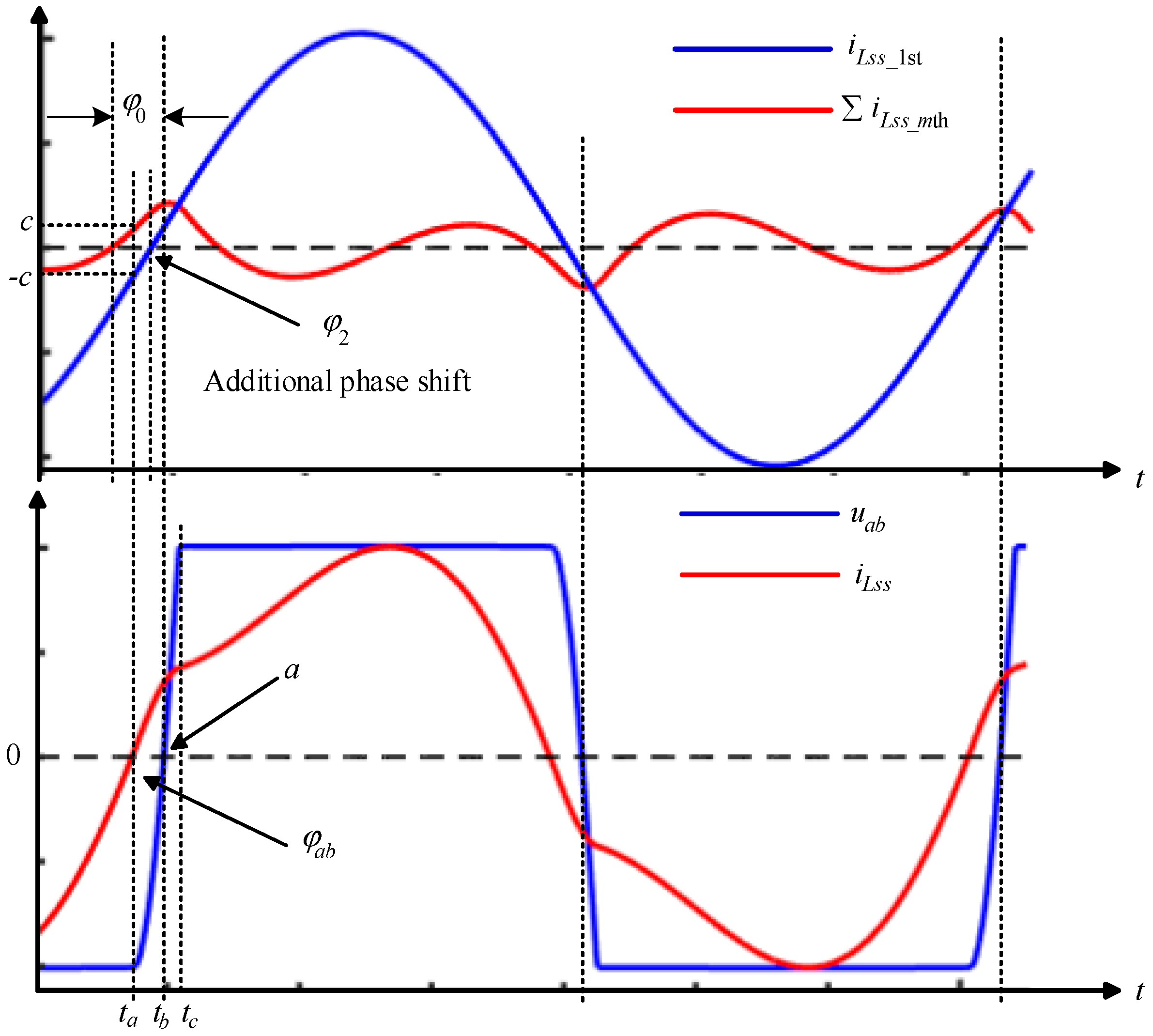
Figure 5.
Theoretical calculation results of the metallic oxide semiconductor field effect transistor (MOSFET)’s turn off current IOFF with different value of Cd: (a) Vo = 300 V, (b) Vo = 400 V and (c) Vo = 450 V.
Figure 5.
Theoretical calculation results of the metallic oxide semiconductor field effect transistor (MOSFET)’s turn off current IOFF with different value of Cd: (a) Vo = 300 V, (b) Vo = 400 V and (c) Vo = 450 V.

Figure 6.
Simulation and theoretical calculation results of the output power for different coupling coefficients: (a) k = 0.3, (b) k = 0.25 and (c) k = 0.2.
Figure 6.
Simulation and theoretical calculation results of the output power for different coupling coefficients: (a) k = 0.3, (b) k = 0.25 and (c) k = 0.2.

Figure 7.
Simulation and theoretical calculation results of the turn off currents for different coupling coefficients: (a) k = 0.3, (b) k = 0.25 and (c) k = 0.2.
Figure 7.
Simulation and theoretical calculation results of the turn off currents for different coupling coefficients: (a) k = 0.3, (b) k = 0.25 and (c) k = 0.2.

Figure 8.
Experimental setup: (a) Picture of the experimental setup and (b) efficiency from power meter at output power of 3.5 kW.
Figure 8.
Experimental setup: (a) Picture of the experimental setup and (b) efficiency from power meter at output power of 3.5 kW.
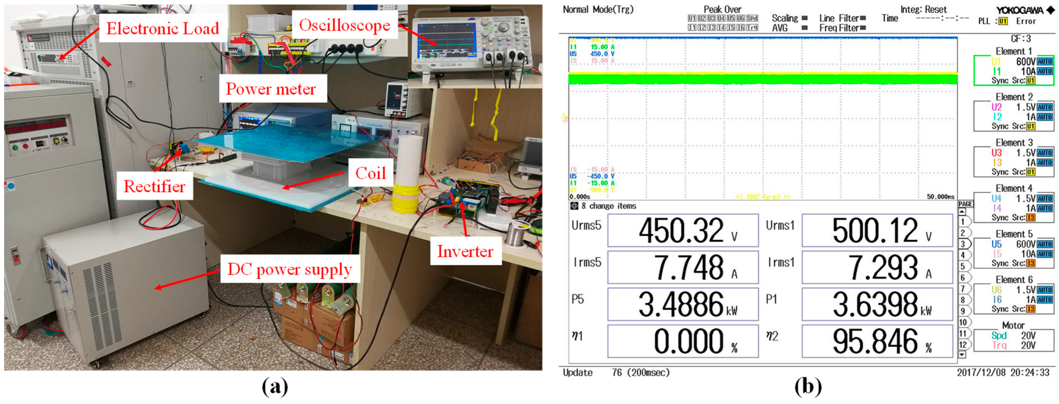
Figure 9.
Theoretical calculation and experimental results of the output power for different output voltages: (a) Vo = 300 V, (b) Vo = 400 V and (c) Vo = 450 V.
Figure 9.
Theoretical calculation and experimental results of the output power for different output voltages: (a) Vo = 300 V, (b) Vo = 400 V and (c) Vo = 450 V.

Figure 10.
Experimental output power of two zero voltage switching (ZVS) tuning methods for different output voltages: (a) Vo = 300 V, (b) Vo = 400 V and (c) Vo = 450 V.
Figure 10.
Experimental output power of two zero voltage switching (ZVS) tuning methods for different output voltages: (a) Vo = 300 V, (b) Vo = 400 V and (c) Vo = 450 V.

Figure 11.
Theoretical calculation and experimental results of the turn off currents for different output voltages: (a) Vo = 300 V, (b) Vo = 400 V and (c) Vo = 450 V.
Figure 11.
Theoretical calculation and experimental results of the turn off currents for different output voltages: (a) Vo = 300 V, (b) Vo = 400 V and (c) Vo = 450 V.

Figure 12.
Waveforms of the input voltage uAB and current iLps and MOSFETs gate driver signals VG1 and VG2 when delivering power of 3.5 kW. Vin = 500 V, and Vo = 450 V.
Figure 12.
Waveforms of the input voltage uAB and current iLps and MOSFETs gate driver signals VG1 and VG2 when delivering power of 3.5 kW. Vin = 500 V, and Vo = 450 V.
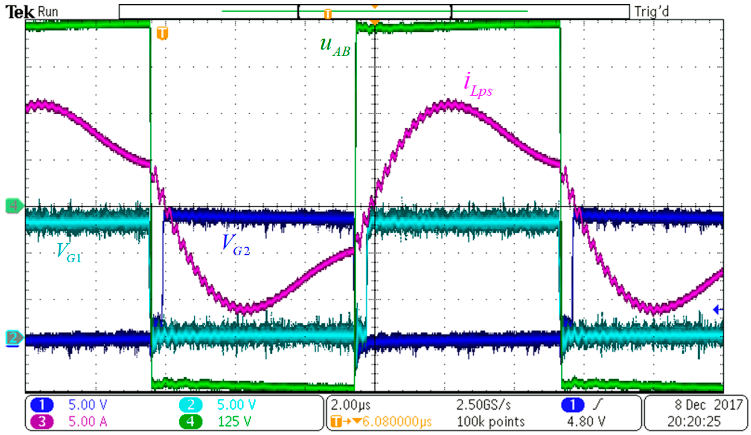
Figure 13.
Experimental turn off currents of two ZVS tuning methods for different output voltages. (a) Vo = 300 V, (b) Vo = 400 V and (c) Vo = 450 V.
Figure 13.
Experimental turn off currents of two ZVS tuning methods for different output voltages. (a) Vo = 300 V, (b) Vo = 400 V and (c) Vo = 450 V.

Figure 14.
Experimental efficiencies of two ZVS tuning methods for different output voltages. (a) Vo = 300 V, (b) Vo = 400 V and (c) Vo = 450 V.
Figure 14.
Experimental efficiencies of two ZVS tuning methods for different output voltages. (a) Vo = 300 V, (b) Vo = 400 V and (c) Vo = 450 V.

Table 1.
Parameters of wireless power transfer (WPT) system.
| Spec/Parameter | Values |
|---|---|
| Input DC voltage | <500 V |
| Output voltage | 300–450 V |
| Nominal gap | 120 mm |
| Coupling coefficient | 0.2–0.3 |
| Transmitting coil inductance | 300 μH |
| Transmitting coil AC resistance | ~500 mΩ |
| Receiving coil inductance | 202.7 μH |
| Receiving coil AC resistance | ~500 mΩ |
| Switching frequency | 85 kHz |
| Maximum power | ~3.6 kW |
Table 2.
Parameters of compensation network.
| Parameter | Values |
|---|---|
| Lps | 97.4 μH |
| Lss | 72.05 μH |
| Cpp | 36 nF |
| Csp | 48.66 nF |
| Cps | 17.3 nF |
| Css | 26.83 nF |
| Cd | 2.8 nF |
© 2018 by the authors. Licensee MDPI, Basel, Switzerland. This article is an open access article distributed under the terms and conditions of the Creative Commons Attribution (CC BY) license (http://creativecommons.org/licenses/by/4.0/).
Share and Cite
MDPI and ACS Style
Lu, S.; Deng, X.; Shu, W.; Wei, X.; Li, S. A New ZVS Tuning Method for Double-Sided LCC Compensated Wireless Power Transfer System. Energies 2018, 11, 307. https://doi.org/10.3390/en11020307
AMA Style
Lu S, Deng X, Shu W, Wei X, Li S. A New ZVS Tuning Method for Double-Sided LCC Compensated Wireless Power Transfer System. Energies. 2018; 11(2):307. https://doi.org/10.3390/en11020307
Chicago/Turabian StyleLu, Sizhao, Xiaoting Deng, Wenbin Shu, Xiaochao Wei, and Siqi Li. 2018. "A New ZVS Tuning Method for Double-Sided LCC Compensated Wireless Power Transfer System" Energies 11, no. 2: 307. https://doi.org/10.3390/en11020307
Note that from the first issue of 2016, this journal uses article numbers instead of page numbers. See further details here.