Insights into Dynamic Tuning of Magnetic-Resonant Wireless Power Transfer Receivers Based on Switch-Mode Gyrators

Department of Electronics Engineering, Technical University of Catalonia UPC, 08034 Barcelona, Spain
*
Author to whom correspondence should be addressed.
Energies 2018, 11(2), 453; https://doi.org/10.3390/en11020453
Submission received: 30 December 2017
/
Revised: 5 February 2018
/
Accepted: 9 February 2018
/
Published: 20 February 2018
(This article belongs to the Special Issue Wireless Power Transfer and Energy Harvesting Technologies)
Abstract
:Magnetic-resonant wireless power transfer (WPT) has become a reliable contactless source of power for a wide range of applications. WPT spans different power levels ranging from low-power implantable devices up to high-power electric vehicles (EV) battery charging. The transmission range and efficiency of WPT have been reasonably enhanced by resonating the transmitter and receiver coils at a common frequency. Nevertheless, matching between resonance in the transmitter and receiver is quite cumbersome, particularly in single-transmitter multi-receiver systems. The resonance frequency in transmitter and receiver tank circuits has to be perfectly matched, otherwise power transfer capability is greatly degraded. This paper discusses the mistuning effect of parallel-compensated receivers, and thereof a novel dynamic frequency tuning method and related circuit topology and control is proposed and characterized in the system application. The proposed method is based on the concept of switch-mode gyrator emulating variable lossless inductors oriented to enable self-tunability in WPT receivers.
1. Introduction
Driven by the high demand of a wide variety of applications, magnetic-resonance wireless power transfer (WPT) has attracted wide interest in research and industry alike. WPT manifests itself as a reasonable solution for applications where contactless power transmission is urgent and preferable. Applications of WPT ranging from low-power (as low as 10 mW) medical implantable devices [1] to high-power (as high as 20 kW) EV charging [2] have benefited from the basic concept of two loosely coupled coils to transfer the power within the near field range. Magnetic-resonance WPT is considered as an inductive coupling supported by resonance in which the transmitter and receiver are allowed to resonate at a common operating frequency. The resonant inductive coupling WPT is well known due to its superior power transfer capability over an extended range while efficiency is still reasonable [3]. Several compensation techniques have been introduced and studied extensively in the literature starting from the simple connection of series or parallel compensating capacitor [4] up to more advanced topologies such as inductor/capacitor/inductor (LCL) [5] and inductor/capacitor/capacitor (LCC) [6].
Considering the simple topology of capacitor-compensated coils, it has been found that the WPT link efficiency is a function of the quality factor Q at the transmitter and receiver circuit [7]. Consequently, the design of high-Q resonant circuits is preferred in terms of efficiency. However, the system becomes more sensitive to any frequency mismatch in case of high-Q resonant transmitter and receiver. Even for small mismatch percentages, the power transfer capability would drop severely and the system would lose functionality [8]. The mismatch in a resonant tank, either at the transmitter or receiver side, originates due to various reasons such as component tolerance, temperature effect on component value, distance variations and interference from proximity devices [9]. To avoid stability issues due to high-Q receiver tank, it has been suggested to limit Q at a maximum of ten such that the system becomes less sensitive for variations and mismatch [3].Therefore, automatic tuning is critical for high-Q systems, ensuring optimal power transfer conditions. Moreover, a self-tuned receiver tank is more practical especially in multiple receiver WPT systems [10].
Different solutions have been proposed in the literature for a seamless tuning of WPT receivers. Among them, Lem et al. [11] proposed an adaptive matching for compensating distance change by means of a switch-capacitor network. Alternatively, Zaheer et al. [12] added a saturable-core inductor in parallel with the compensating capacitor where the resonant frequency could by continuously tuned. Similarly, Si et al. [13] have used a capacitor to be switched dynamically in parallel with the receiver in order to change the effective value of the capacitor, so that the resonance frequency can be tuned. On the other hand, Pantic et al. [9] have leveraged a novel tri-state boost converter to be used as means of real power regulation while injecting a negative or positive reactance to the receiver tank.
This paper, considered as an extended version of the work presented in [14,15], proposes the concept of gyrator-based dynamic tuning of parallel-compensated WPT receivers. The fundamentals of tuned and mistuned parallel-compensated WPT receivers are discussed in Section 2. Following that, the concept of dynamic tuning by means of gyrator-based reactance is presented in Section 3 and Section 4. Driven by the design of gyrator-based reactance, a closed-loop dynamic frequency tuning is given and verified in Section 5. Moreover, the chip design implementation for the proposed gyrator-based dynamic tuning is given in Section 6. Finally, system design considerations and technical limitations are discussed in Section 7.
2. Parallel-Compensated WPT Receivers
Magnetic-resonant WPT is characterized by tuning the transmitter and receiver coil using a capacitor connected either in series or parallel; hence the name “series-compensated” or “parallel-compensated” respectively. There are different compensation topologies depending on the connection of the capacitor at the transmitter and receiver, such as series-series, series-parallel, parallel-series and parallel-parallel. The power transfer capability and characteristics of each topology has been extensively discussed in [4]. From the load perspective, a series-compensated receiver coil is normally used for low-voltage application in which the receiver has voltage source characteristics combined with a current boosting capability. On the other hand, a parallel-compensated receiver is suitable for most applications due to the inherent capability of voltage boosting which extends the system operation at very weak coupling conditions while still meeting the load voltage requirement [16]. Therefore, this paper focuses on the discussion of mistuning issues in parallel-compensated WPT receivers in which the proposed dynamic tuning solution is dedicated for the same.
2.1. Principles of Parallel-Compensated WPT Receivers
In parallel-compensated WPT receivers, the receiver coil LR is compensated by a capacitor CR connected in parallel to enable the receiver to resonate precisely at the transmitter frequency fT. Considering the simplified model given in Figure 1, the open-circuit induced voltage Voc is commonly modeled as a voltage source in series with LR. While the receiver circuit is usually loaded by a rectifier followed by a voltage regulator, it is widely accepted to assume a resistive load RL for the sake of simplicity. The voltage ratio of the receiver parallel resonant tank (Vac/Voc) is given by:
where Vac is the receiver resonant tank output voltage, , , M is the mutual inductance between the transmitter and receiver coils, ωT is the transmitter angular frequency and IT is the transmitter coil’s current. Given the resonance frequency of the receiver tank as:
at fully-tuned case, (i.e., the resonance frequency of the receiver tank is equal to the transmitter frequency ), then Equation (1) can be reduced with the help of (2) as:
where QRL is the receiver’s quality factor. Equation (3) shows that the resonant tank voltage is boosted from the open-circuit induced voltage by a factor that is equal to the quality factor QRL. On the other hand, the power transmitted to the receiver is a function of the reflected impedance from the receiver to the transmitter circuit. The reflected impedance is a function of the input impedance of the receiver tank, as seen by , defined as:
and the impedance reflected back to the transmitter is expressed as follows:
where Zref is the receiver impedance seen by the transmitter, and Rref, Xref are the real and imaginary parts of the reflected impedance respectively. Thus, the expressions for Rref and Xref are derived as:
Similarly, at fully-tuned case the transmitter angular frequency ωT is equal to Equation (2), Equations (6) and (7) reduce to:
Equations (8) and (9) declare that the reflected impedance is a function of M which represents the coupling between the two coils. Another fact revealed by Equation (9) is that a nonzero reactance is reflected to the transmitter. The nonzero reflected reactance is an important characteristic that should be taken into account during the design of the compensation circuit at the transmitter side. On the other hand, the power transmitted to the receiver is the power dissipated into the real part given in Equation (8), which reaches a maximum at fully-tuned condition. The maximum power delivered is written as [12]:
2.2. Mistuning Effect on Power Delivery
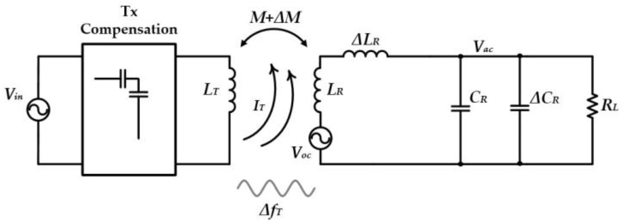
The maximum power in Equation (10) refers to the load dependency; moreover, power transfer capability is greatly enhanced with higher quality factor QRL. However, the receiver circuit becomes more sensitive for any variations as QRL increases. To illustrate the mistuning effect on the receiver circuit, Figure 1 depicts possible variations in LR or CR modeled as ∆LR and ∆CR respectively. Note that ∆CR (or ∆LR) comprises either positive or negative values (i.e., presuming over-tuned or under-tuned conditions). Including such variations implies that the resonance frequency of the receiver tank is either shifted to lower or higher values compared to the value given in Equation (2). Consequently, one can conclude that Vac and Pmax in Equations (3) and (10), respectively, are not relevant anymore. By including all the prospective mismatch sources altogether, it is possible to predict the accurate performance of the receiver tank. The obtained equations, however, would be cumbersome. Therefore, a simple case of variation ∆CR in the compensation capacitor is assumed, as shown in Figure 1, in which ∆CR presumes positive or negative values.
Firstly, the capacitor variation ∆CR is included in Equation (1) in which the voltage boosting ratio turns into:
assuming that the transmitter frequency ωT is constant and complies with Equation (2), then the rms value of Equation (11) is given by:
where () is the capacitance mismatch ratio. By comparing Equations (3) and (12), it is apparent that the voltage ratio of the receiver tank drops to a lower value due to the capacitance mismatch. It is even worse for ultra-high QRL receiver circuits. Moreover, the mistuning effect on the delivered power has to go through the reflected impedance expressions in Equations (6) and (7) that become:
In a similar way, recalling that (ω = ωT) reduces Equations (13) and (14) to:
Once more, while paying more attention to the real part in Equation (15), the mistuning factor multiplied by a factor of results in a significant drop in the resistance reflected back to the transmitter. This necessarily appears as a serious drop in power delivery at the receiver circuit which is obvious by comparing Equation (10) with the new expression of delivered power:
The given power delivery in Equation (17) is not actually applicable unless the transmitter circuit is equipped by an adaptive tuning circuit to compensated for the modified reflected reactance in Equation (16). Otherwise, the transmitter circuit would be left with some amount of uncompensated VAR that would deteriorate the power transfer from another side.
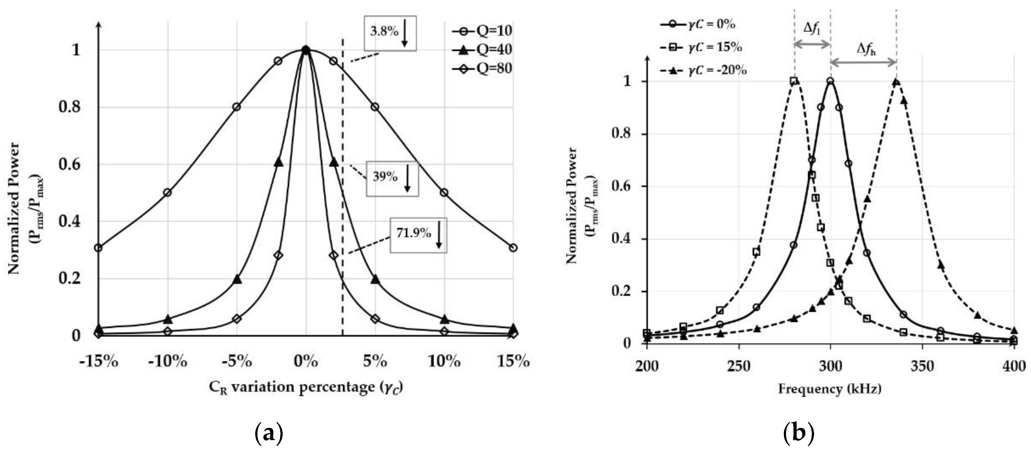
A clear consequence that arises from Equation (17) is that a significant drop in transferred power is inevitable as long as the receiver circuit is designed for high-Q operation. The effect of capacitance variation on the transferred power is shown in Figure 2a, where the normalized power (Prms/Pmax) is plotted against for three different values of QRL. It is obvious that the drop in power due to a small mismatch percentage of 2% is becoming noticeable for high-Q values. As noted in Figure 2a, the high-Q receiver circuit becomes extremely sensitive irrespective of the enhancement in power transfer capability at the tuned point. The case of QRL = 80 is an illustrative example in which a 71% drop in Prms is expected for a 2% mismatch in CR. On the other hand, Figure 2b depicts the frequency drift by ∆fl as a result of 15% mismatch while it drifts to a higher frequency by ∆fh amount due to −20% mismatch. As a direct result, in order to overcome the pitfall of high-Q receivers, the QRL is normally limited to less than 10 in most systems particularly for high power applications [3]. This, however, is not an adequate choice for low power applications that would demand energy from a distance that extends up to a few times the coil diameter. In the next section, we introduce a novel approach for dynamic frequency tuning of high-Q parallel-compensated WPT receivers to mitigate the mistuning effects.
3. Dynamic Tuning by Means of Gyrator-Based Reactives
In order to counteract the mistuning in WPT receivers, the resonance frequency of the receiver tank can be re-tuned by means of an additional corrective inductive or capacitive element. Obviously, the added element has to be an active element where the feature of tunability is met.
3.1. Generalized Model for The Proposed Dynamic Tuning Approach
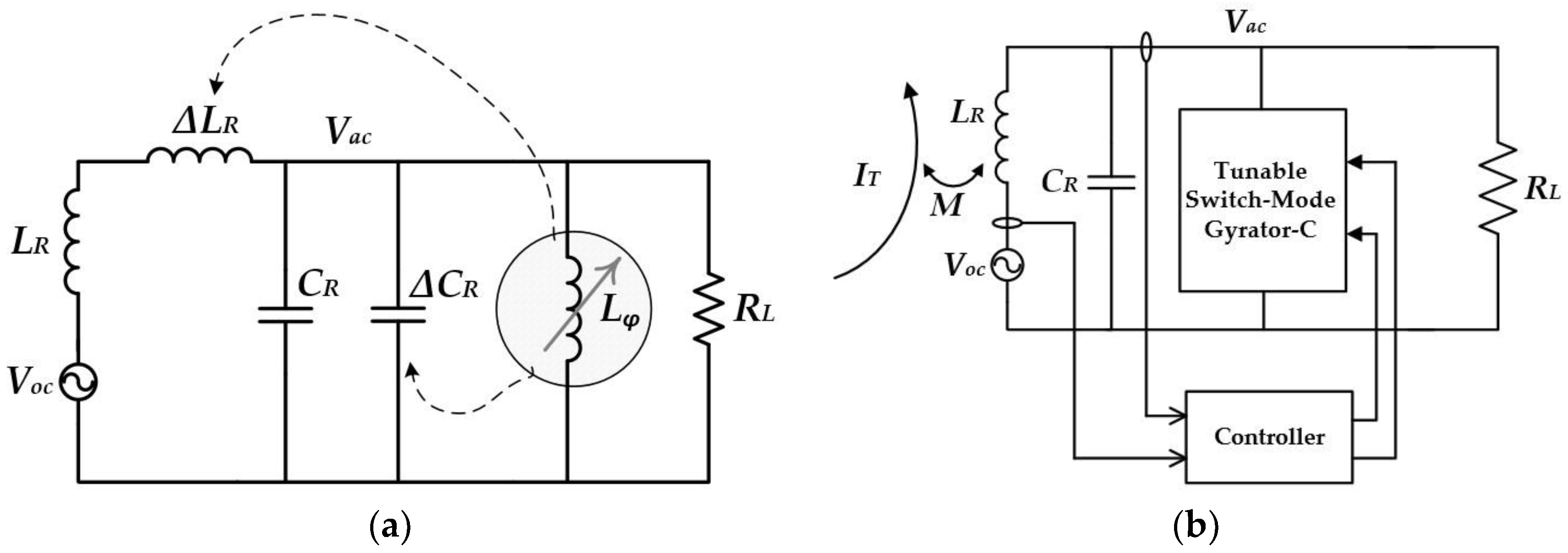
Provided that we have no access to the physical values of receiver’s coil and compensation capacitor once the system is already functioning in practice, one way to dynamically tune the resonance frequency ωR of the receiver tank is to add a tunable active reactance to the circuit. A model for the WPT receiver with the connection of a variable inductance is illustrated in Figure 3a. The variable inductance Lφ is connected in parallel with the compensation capacitor. Therefore, it can be deemed as an additional inductance connected in parallel with the receiver coil LR (and ∆LR) in essence. By referring to the Figure 3a, then, a new parameter evolves as a combination between the added inductance Lφ and CR:
where CφR is the equivalent capacitance that includes the inductive behavior of Lφ. In accordance to Equation (18), the new expression for the resonance frequency of the receiver tank becomes:
where ωR0 is already given in Equation (2). Since the new resonance frequency in Equation (19) is a function of Lφ, it indicates that ωR can be tuned over a wide range that is only limited by the tuning range of Lφ. With the help of Figure 3a, including all the depicted mismatches (∆LR, ∆CR), the power transferred to the receiver is calculated as:
where γL = ∆LR/LR and γφ = ∆CR/Cφ. Clearly, the transferred power in (20) can be recovered to the maximum, nearly as given by Equation (10), by tuning Lφ and thus CφR subsequently. Thereby, the mistuning effect incurred by γL and γφ could be neutralized.
3.2. Impedance Emulation By Means of Gyrators—A Spotlight
The general approach of adding a variable reactive element in parallel with the receiver tank has been developed in [17] by means of a phase-controlled inductance and in [12] by means of a saturable-core reactor. Nevertheless, the phase-controlled reactor has been introduced in the framework of detuning the receiver circuit at light-load condition, which is undoubtedly far from our objective. On the other hand, the saturable-core approach is incompatible with size and weight constraints of low power portable applications.
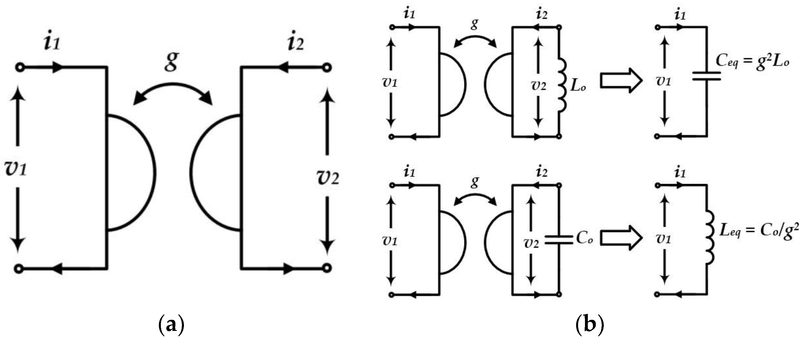
The gyrator in Figure 4a, as a theoretical concept, has been firstly proposed by D. H. Tellegen in the domain of a new network element added to the four known elements [18]. Since that date, the gyrator has become a reliable element for a wide range of applications. Promoted by its characteristics as a two-port, lossless, linear, and power-conservative element, the gyrator offers a unique property of transconductivity highlighted by its input-output relations:
where g(t) is called “gyrator conductance”. Implied by Equation (21), the gyrator has the capability of duality transformation for any element from one port to the other, e.g., inductive to capacitive reactance and capacitive to inductive reactance is possible as illustrated in Figure 4b. Given a capacitive reactance coupled to the output port of a gyrator, an inductive reactance is viewed at the input port, as follows:
where Co is the capacitance connected to the output port and Leq is the equivalent inductance as seen by the input port. Indeed, this unique property has been of valuable importance for many applications such as RF filter design in which the replacement of on-chip bulky inductors by a gyrator-C circuit is a cutting-edge solution [19].
Gyrator circuit realization was, and is still, a rich topic of research in literature. Several successful implementations has been proposed. For instance, transistor-based realization [20], linear amplifier based [21], and current conveyor based [22] are among the most popular realizations. Yet, such implementations are lossy linear amplifier-based. Consequently, they are not adequate for power processing applications where efficiency is a must. In the next section, topology candidates for power gyrator realization are discussed.
4. Switch-Mode Gyrator-Enabled Variable Inductance
4.1. Gyrators in Power Processing Applications
Loss-free gyrator implementation has been enabled following the rapid development in switch-mode power processing circuits. A gyrator, as a power conservative element, could be theoretically implemented by any power-out-equals-power-in circuit (POPI) such as buck, boost, and flyback converters [23,24]. In order for a POPI circuit to be “gyrated”, i.e., to operate as a gyrator, the output current could be controlled proportionally with the input voltage in circuits that enjoy a continuous output current such as buck converter [23]. In contrast, the input current needs to be controlled with respect to output voltage in continuous input current topologies such as boost converter.
Clearly, for a circuit to behave as a gyrator, it is obtainable either through topology-based implementations like in the case of two back-to-back transconductors or through control-based realization. Interestingly, dual bridge converters (DBC) is a family of switch-mode converters that belongs to the first kind, i.e., topology-based gyrators. The dual active bridge converter (DAB) is a DBC switch-mode converter that is well-known as a control-free naturally gyrated converter [25]. By using the DAB as control-free gyrator, the effort of forcing the gyration behavior could be saved in favor of designing a simple control to tune the value of a DAB-based synthesized reactance. In the next subsections, the operation and adoption of DAB as a variable reactance synthesizer will be discussed.
4.2. DAB as a Switch-Mode Natural Gyrator—Revisiting
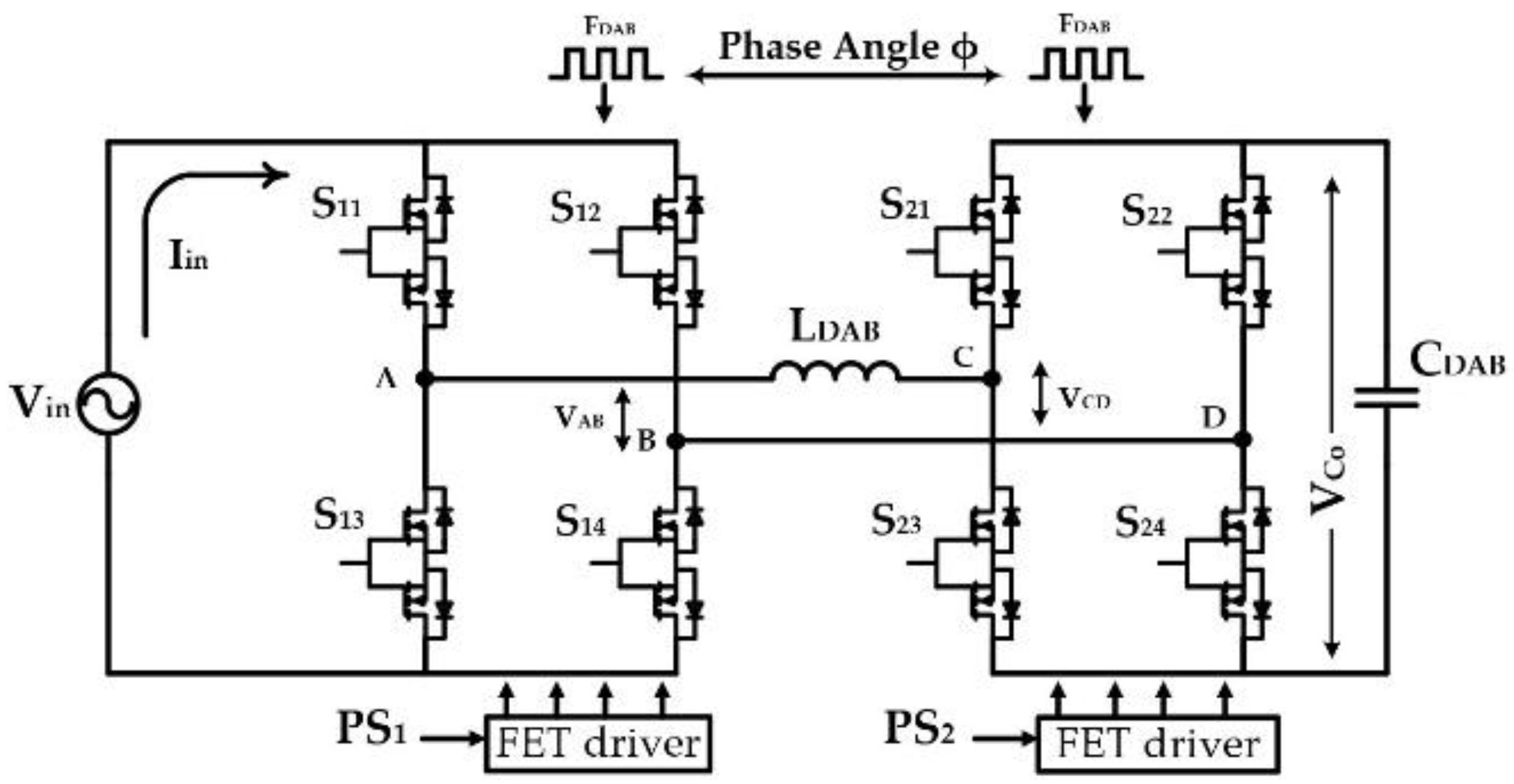
The DAB converter is a bidirectional topology that benefits from the concept of what is called “AC inductor” where the average inductor current is zero [26]. The operation of the DAB converter as a candidate topology for inductive reactance synthesis has been discussed, in detail, in [27] and [28]. Shortly described, the DAB converter is composed of two full-bridge structures (S11–S12–S13–S14 bridge and S21–S22–S23–S24 bridge in Figure 5) linked by an AC inductor LDAB. Moreover, it is a bidirectional topology where the power flow direction is guided by the relative phase-shift (φ) between the two bridges.
The DAB converter has been primarily introduced as a DC-DC converter for the purpose of power processing where all the converter switches shown in Figure 5 could be realized by a two-quadrant IGBT or MOSFET switches [29]. However, for the purpose of variable reactance synthesis using the same converter, the converter has to be capable of processing bidirectional ac voltages. Thus, the DAB converter must allow bidirectional current flow and voltage polarity [30]. Therefore, four-quadrant switches, e.g., back-to-back source connected MOSFETs, have been used to realize all the switches as shown in Figure 5. In essence, either the input or output bridges could be treated as a matrix converter equipped with four-quadrant AC switches [31].
As a natural gyrator, the gyration conductance following the analysis in [25] is given by:
where ωDAB is the angular switching frequency of the converter, LDAB is the link inductance, and φ is the phase-angle between the switching operation of the two bridges. Considering the capacitive load CDAB at the output, then the seen inductance at the input port is given as:
The synthesized inductance Lφ is a function of circuit parameters, in which tunability is achieved by either varying the switching frequency ωDAB or the phase-angle φ in Equation (24). Obviously, varying the switching frequency would complicate the process of control design, therefore varying the phase-angle is more reasonable and appropriate in terms of design reliability.
4.3. DAB-Based Variable Inductance Design
As a design example, in this section a DAB-based variable inductance is designed to showcase the validity of the concept. A sinusoidal input source with frequency of 300 kHz is applied to the input of the DAB. The switching frequency fDAB is affecting the design parameters while at the same time there is a perpetual trade-off between the circuit performance, efficiency and the switching frequency [32]. The higher the switching frequency is, the lower LDAB and CDAB for the same required Lφ become. For the specified input frequency, a switching frequency of 5 MHz is chosen in order to decrease the amount of ripple while maintaining lower LDAB and CDAB. The circuit parameters are given in Table 1, in which the circuit in Figure 5 has been characterized using the event-based PSIM simulation framework. Figure 6a indicates the gyration behavior of the four-quadrant DAB converter, in which the inductor current ILDAB, the input bridge voltage VAB, the output bridge voltage VCD, and the DAB output voltage VCo are shown for the case of φ = 50°. The estimated value of synthesized inductance Lφ at φ = 50° is nearly 36 μH. It is observed in Figure 6a that the average current of LDAB is zero. Moreover, the input current of DAB is bipolar (Iin is not shown in the figure) and discontinuous. However, it is still valid to infer the input current ILDAB by referring to the DAB output VCo as an indication, a fact that is derived from the gyrator characteristic equation (iin = g·vo). Therefore, the gyration behavior is denoted by the quadrature phase lag (in Figure 6a) between the DAB output voltage VCo and the input voltage Vin.
With regards to tuning capability, the phase-shift angle has been swept from 30° to 150° and the synthesized inductance Lφ as well as the gyration conductance g versus φ is shown in Figure 6b. Although Lφ is theoretically amenable to full–range tuning of 0–180°, it has been noted that the synthesized inductance approaches very high values of φ < 20° or φ > 150°. Note that the shown data in Figure 6b is limited to the range of 40–130° for the sake of clarity. The given results are comparing the calculated values of g and Lφ as given in Equations (23) and (24) with the values obtained by circuit simulation. The figure shows a good correlation between the calculated and simulated verification. Indeed, the mismatch between the calculated and simulated values is due to the losses of the AC switches that are included in the simulation circuit while lossless circuit components have been considered in the theoretical expressions. Worthwhile, the gyration behavior in Figure 6b replicates symmetrically around φ = 90°, which closely correlates with Equation (23). This symmetry reveals that the synthesized inductance has only two valid tuning ranges either φ = 0°–φ = 90° or φ = 90°–φ = 180°. This fact should be taken into account in the process of designing a bidirectional tuning system for WPT receivers.
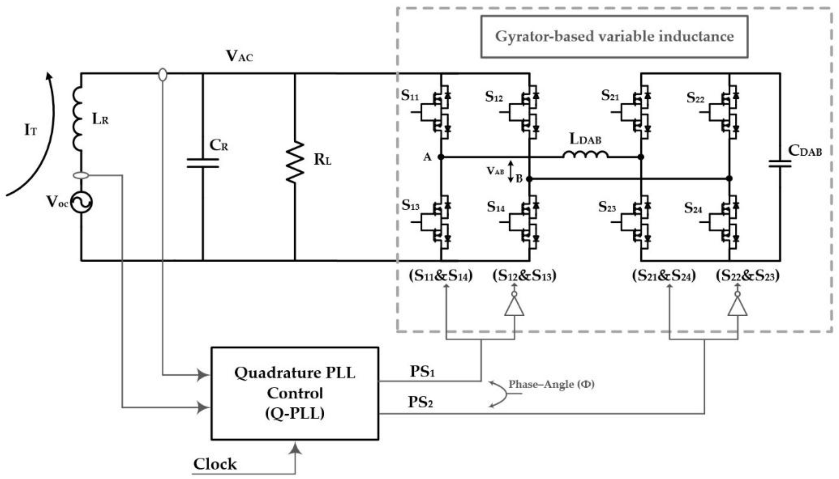
5. Implementation of Dynamic Frequency Tuning Control
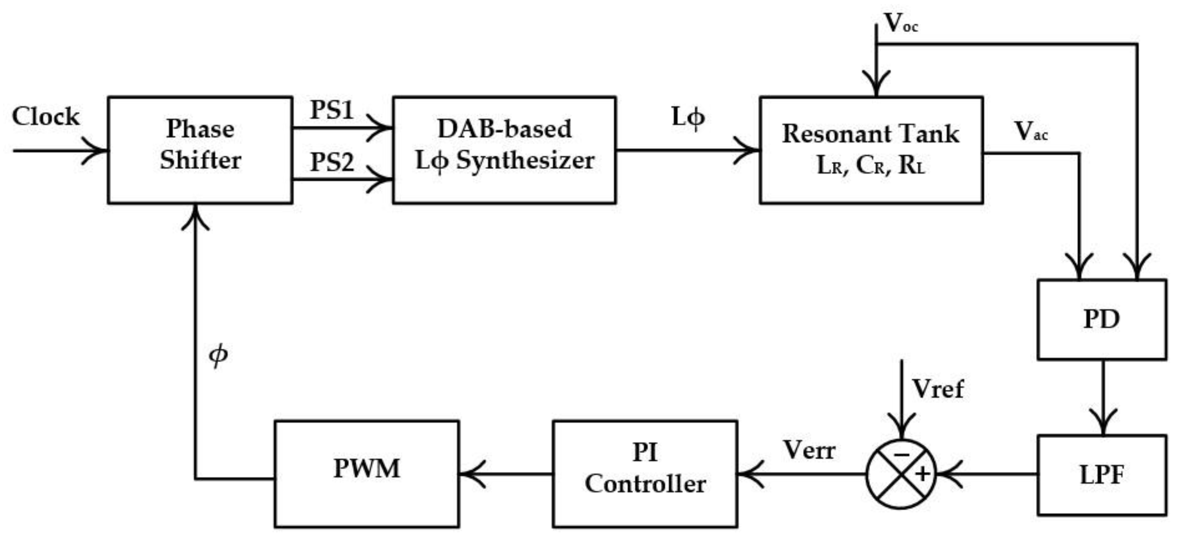
Figure 7 shows the block diagram of the parallel-compensated WPT receiver after adding the DAB gyrator as a tunable inductance synthesizer. In order to verify the dynamic tuning capability of the approach, a quadrature phase-locked loop (Q-PLL) control was designed. The details and operation of the Q-PLL control is to be discussed in the next subsection.
5.1. PLL-Like Control—Theory and Operation
The ultimate goal of the controller is to guarantee autonomous dynamic tuning for the WPT receiver irrespective of any variations that would give rise to a mistuned tank, such as the variations that have been discussed in Section 2. The controller finds out whether there is a mistuning in the WPT receiver, then responds accordingly by fine-tuning the phase-angle φ of the DAB converter such that the corresponding Lφ for retuning is dynamically achieved. A parallel-compensated WPT receiver, while in fully-tuned state, holds two facts as indicated by Equation (3): (a) the resonant voltage Vac is equal to a maximum value given by the induced voltage Voc boosted by QRL; (b) Voc leads Vac by 90°. We have verified in [14] that accurate retuning cannot be achieved by utilizing merely the first fact, i.e., the maximum Vac = QRL·Voc. Therefore, the Q-PLL control takes advantage of the second fact, which is dependent on the quadrature phase difference between Vac and Voc at fully-tuned state. To examine this fact, the transfer function of the parallel WPT receiver after adding the DAB variable inductance Lφ is given as:
Regarding this proposal, it is of interest to examine the phase angle between and by converting Equation (25) to the polar form. The phase angle can be expressed as:
where is the phase angle between and . For to be equal to 90°, the right-hand term of Equation (26) has to approach infinity. In other words, the denominator of Equation (26) becomes:
It is evident that for the angle in Equation (26) to be equal to 90°, the denominator in Equation (27) has to be equal to zero, which is only possible if Lφ is adjusted such that the tank is fully-tuned {ωT = (Lφ + LR)/LφLRCR}. Consequently, the control has to be designed as quadrature PLL-like, hence the name “Q-PLL”. The control operates by sensing Vac and Voc and acts by tuning φ toward steady-state fully-tuned state fulfilled once Vac lags Voc by 90°. The control block diagram in Figure 8 comprises an XOR phase-detector (PD), low-pass filter (LPF), an error amplifier compensated by a proportional-integral (PI), pulse-width modulator (PWM) block, and finally a phase-shift modulator (PSM).
In order for the control to work properly, the desired tuning range has to be designed according to the WPT receiver parameter, e.g., operating frequency fT and coil inductance LR. Note that the tuning range of DAB-based synthesized inductance Lφ as shown in Figure 6b is unidirectional, either from 0° to 90° or from 90° to 180° as implied by the symmetrical gyration behavior around φ = 90°. In order to allow a bidirectional tuning range, the Lφ has to be designed at the middle of the gyration curve, e.g., φ = 50°, to resonate with LR and CR at the nominal operating frequency fT. Therefore, tuning ranges of (0°–50°) and (50°–90°) are enabled depending on the sign of mismatch either in γL or γC.
5.2. System Integration and Validation Results
The dynamic frequency tuning approach declared in Figure 7 has been characterized and validated by simulation for the design specification parameters given in Table 2. The values of WPT transmitter coil LT and receiver coils LR have been designed to deliver about 500 mW to 200 Ω load at a coupling coefficient of k = 0.1 while operating at 200 kHz.
The transmitter coil LT has been compensated by a series capacitor CT of 63.97 nF taking into account the reflected negative reactance (100 nF at coupling coefficient of k = 0.1) from a fully-tuned receiver as given by (9). Correspondingly, the DAB gyrator parameters have been designed and given in Table 2. As pointed out in the previous subsection, it turns out that for a wide bidirectional tuning range by means of the DAB gyrator inductance, the synthesized inductance Lφ has to be designed in order to resonate with LR and CR while a sufficient φ tuning margin is allowed. Therefore, the synthesized inductance Lφ has been optimized at a value of 8.08 μH at φ = 45°. The DAB circuit is switching at the rate of 1.5 MHz which is reasonably higher than the link signal frequency fT. A higher switching frequency would be beneficial in terms of the required values for LDAB and CDAB, as suggested by (24). As a typical phenomenon in switch-mode circuits, the internal losses of the DAB circuit would increase proportionally with the switching frequency leading to the trade-off between components size and efficiency.
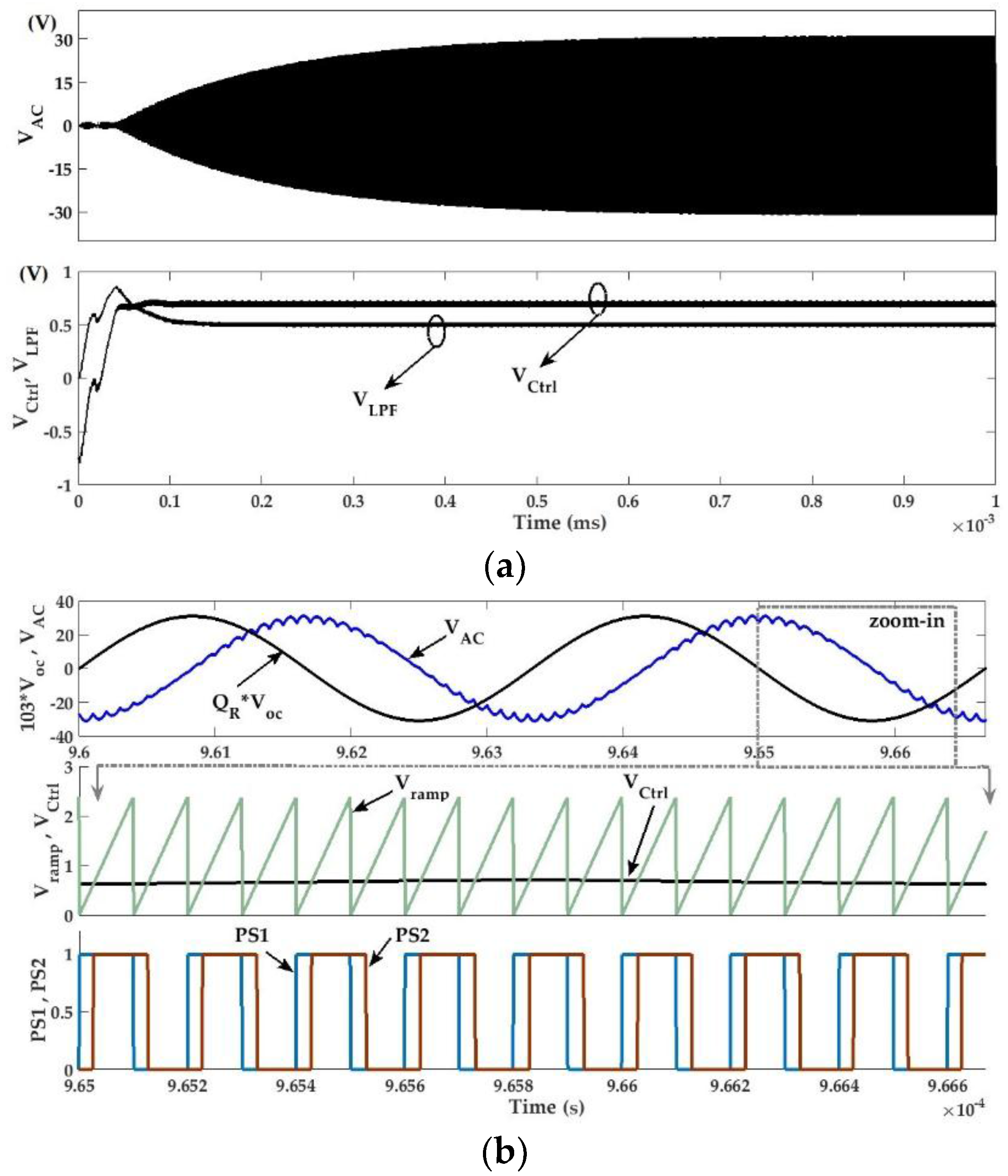
Following the system parameters design, the Q-PLL control for dynamic tuning has been implemented as shown in the block diagram in Figure 8, in which the components values are annexed to the same figure. Figure 9a shows the transient waveforms of the resonant tank voltage Vac where it shows that the tank voltage builds until it reaches the maximum at fully-tuned state. Also, the same figure shows the Q-PLL control signal VCtrl and the corresponding control input variable VLPF. It is evident that VLPF, which represents the phase difference between Vac and Voc, reaches Vref = 0.5 V indicating that Vac lags Voc by 90° as the typical state of a fully-tuned parallel resonant tank. Moreover, Figure 9b shows a close-in view for the steady-state waveforms for which the phase difference between Vac and Voc (scaled by QRL) is highlighted. Figure 9b shows, as well, how the duty-cycle generated by the control is translated to the corresponding phase-angle φ (almost 45° at the specified system parameters in Table 2) between the gating signals PS1 and PS2.
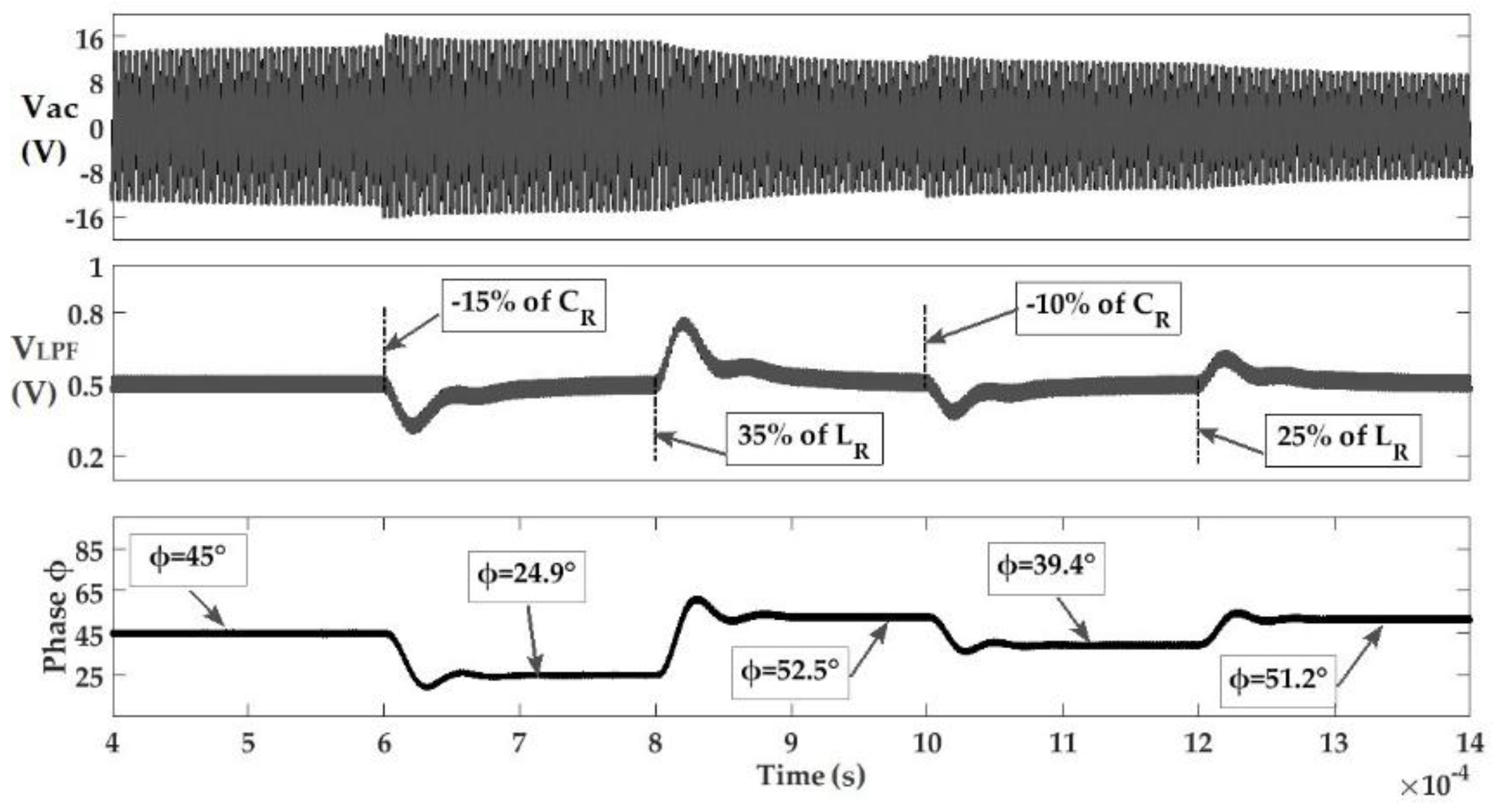
Figure 10 shows the performance of the gyrator-based dynamic tuning approach in response to mismatch in CR and LR. The system operation for −11% mismatch in CR followed by −11% mismatch in LR is given in Figure 10a, in which the figure shows how φ is dynamically controlled to retune the resonant tank. To neutralize the undercompensation effect of decreased CR and LR, the effective synthesized Lφ has to be increased which is apparent in the phase-angle stepping down from the nominal value of Lφ = 45° (refer to Figure 6b). Moreover, Figure 10b indicates the system performance for an increase in CR and LR for the same amount of +11%. Once more, the controller acts by increasing φ to counteract the overcompensated tank by lowering the effective value of Lφ. In order to be able to track the variation imposed by the controller in φ, the phase difference between PS1 and PS2 is sensed and filtered, and subsequently it is post-processed to show the phase-angle in degrees.
Figure 11 aims to show the wide tunability and robustness of the suggested approach in response to irregular successive changes in CR and LR. As pointed out earlier, the allowable tuning range is limited by either the phase-angle φ of DAB-based inductance or by a saturated control output. This effect is to be discussed in the next section.
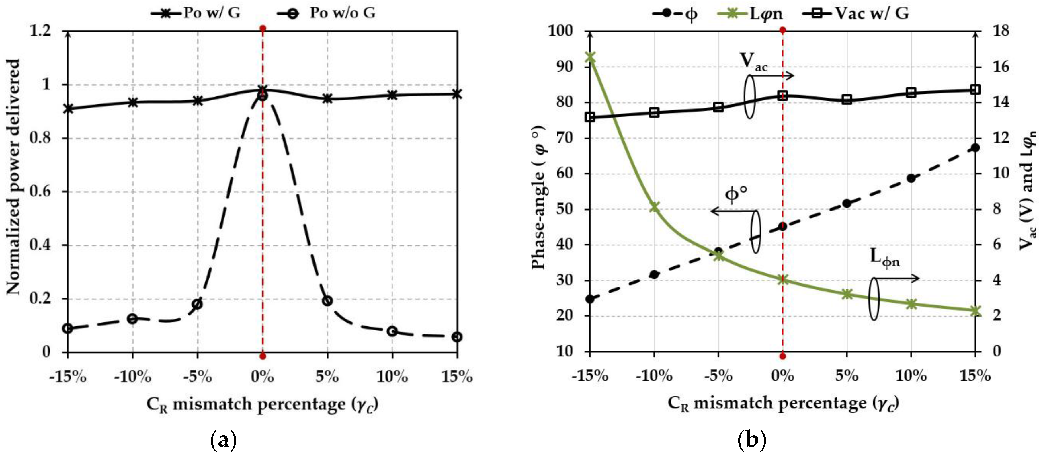
Figure 12a shows the normalized power delivered versus different CR mismatch percentages with and without the gyrator-based synthesized inductance at RL = 200 Ω (system specifications defined in Table 2). By comparing the normalized received power with using the gyrator-based dynamic tuning, it is evidenced that the system is successfully capable of compensating the mismatch effect by tuning the synthesized inductance. It is noted that the delivered power at γC = 0% is almost the same either with or without the dynamic tuning approach, which is because the receiver parameters have been optimized at fully-tuned condition in the nominal case of no mismatch. Nonetheless, we note that the delivered power drops slightly with using the gyrator-based dynamic tuning due to the losses of the DAB converter that affect the tank analogously as being the series resistance of Lφ. Further, Figure 12b shows the optimal phase-shift φ and the corresponding synthesized inductance Lφn (normalized to the LR). We note that at no mismatch, i.e., 0% on the plot, the corresponding Lφ is approximately four times the coil inductance LR which is nominal value at φ = 45° for the optimized parameters in Table 2. Moreover, it is interesting to notice that φ extends from 24.7° to 67.3° approximately for a mismatch range ±15% of CR, which is far enough from the theoretical limit of φ from 0° to 90°. This implies that the dynamic tuning range extends arbitrarily beyond the verified range of ±15%. The resonant tank RMS voltage Vac is plotted versus γC to show that the tank is fully-tuned in response of the mismatch in CR. Again, we note that there is a slight change in Vac due to a slight drop in QR due to losses in DAB.
6. Chip Implementation for the Proposed DAB-based Inductance Synthesizer
In order to reduce the size of the proposed DAB-based dynamic frequency tuning, the target of fully integrating the DAB cell and the Q-PLL control on a single silicon die is of crucial interest. Given the system parameters in Table 2, a full chip implementation becomes feasible in terms of size and performance. Figure 13 shows a schematic diagram for the main parts inside the chip. The receiver coil LR, the compensation capacitor CR, the output load RL, the DAB inductance LDAB, and the DAB output capacitor CDAB are planned as off chip components. All the other components including the DAB power switches and the Q-PLL controller could be integrated into a single chip.
The chip implementation is realized by a 0.18 μm BCD process. High-voltage triple-well isolated MOSFETs are used for realizing the power switches. As shown in Figure 13, two back-to-back switches sized at (60,000 μm/0.35 μm) are used to implement every AC switch. It has been verified through the accurate models of the process that the nominal channel resistance of every AC switch is around 22 mΩ. Consequently, with four AC switches closed simultaneously (two at every bridge), a total conduction resistance of 88 mΩ is included in the loop. The higher the channel resistance of a power MOSFET, the more power it consumes. The channel resistance of every switch could be decreased by sizing the power MOSFETs at higher width. However, this will be at the expense of the total chip area and switching losses. Note that the details of transistor-level design of control blocks are not shown in Figure 13. However, the power consumption of control circuits are verified on Cadence Virtuoso using the accurate models offered by the foundry. The total power consumption of the control is 74.8 mW.
The non-ideal yet functional waveforms of the designed chip are shown in Figure 14. A phase-lag of 90° between Vac and Voc is clear in Figure 14a, where the phase-difference output (VPD) demonstrates this fact. Moreover, the averaging circuit output (VLPF) reaches a steady-state value of 900 mV represent the average of VPD. Note that, when the receiver tank is tuned, VPD has 50% duty-cycle while its high-level is at 1.8V due to the implementation of the phase-difference circuit using 1.8V low-voltage devices. Furthermore, Figure 14b shows the real-time results of the controller signals including error amplifier output VCtrl compared to a ramp signal VST. A comparator realized by a fast folded-cascode wide-swing stage is used to compare VCtrl with VST and the Vduty output is then translated to the phase-shift φ between the driving signals of the DAB circuit.
With using coupled-coils model in Cadence for the coupling between the transmitter and receiver, the total power delivered to the receiver is 5 W. The real power that is consumed by the load (RL = 50 Ω in Figure 13) was 3.74 W, this leads to an estimated efficiency of 74.8%. The total power loss of the chip counts up to 1.26 W which is divided into 74.8 mW (1.5% of total power) in the controller and 1.185 W (23.7% of total power) consumed by the DAB power switches. It is noted that the higher power consumption is due to the losses of power switches. However, the DAB losses can be decreased by up-sizing the width of the DAB power MOSFETs at the expense of more silicon area. The designed chip has been tested over a wide range of variation in LR and CR (−10% to +10% in ∆LR and ∆CR) and the rms power delivered to the load is shown in Figure 14c. It is noted that load rms power is slightly affected by the variations due to the effect on the total quality factor of the receiver tank. The efficiency given in Figure 14c has been calculated as (PL/PR) where PL is the power consumed by the resistive load RL and PR is the actual power received by the WPT coil LR. While the quiescent power consumption by the control circuits stay almost constant at 75 mW, we found that the power consumption of the DAB power switches is main contribution to the losses. A minimum efficiency of 73.4% has been found at ∆CR of +10%. Though, still the total power recovered by the DAB-based dynamic tuning approach is promising compared to a mistuned WPT receiver tank.
7. System Design Consideration—Performance Discussion
7.1. Efficiency and Quality Factor
The analytical expressions that have been provided earlier in Equations (18)–(20), assumed an ideal circuit with loss-free components including the gyrator-based synthesized inductance. In practice, the losses related to circuit components—such as coils, capacitors, switch-mode DAB, rectifier and any other circuit in the power path—have a significant effect on the quality factor of the resonant tank and, in turn, upon the WPT link efficiency. The loss analysis and efficiency evaluation including most of non-idealities in the receiver circuit has been previously discussed in [33]. The quality factor as a definition—the ratio of stored energy to the lost energy—is a valid implicit indication for the efficiency of a circuit. Referred to our parallel-compensated WPT receiver, it is well known that the power transfer link efficiency can be given in terms of the quality factor as [7]:
where QT is the transmitter coil’s quality factor, QRL is the quality factor of the receiver circuit as given in Equation (3), QR is the quality factor of the receiver coil and k is the coupling factor between transmitter and receiver coils. The total efficiency given in Equation (28) is only given to highlight how other components losses would affect the power transfer efficiency. In order to investigate the effect of the gyrator losses, the receiver circuit is analyzed from the perspective of quality factor using the model shown in Figure 15. In this model, we include the receiver coil series resistance RR, the load resistance RL, and the gyrator losses modeled as a resistance Rφ in series with the synthesized inductance Lφ. To facilitate the analysis, the circuit can be converted to the Norton equivalent as shown in Figure 15, where Lφp, LRp, RRp and Rφp are given by:
where (LRp, RRp) and (Lφp, Rφp) are the equivalent values of (LR, RR) and (Lφ, Rφ) after converting the series networks to a parallel networks, while QR and Qφ are the quality factors of LR and Lφ respectively. At fully-tuned state (ωR given by Equation (19)), the resonant voltage of the circuit in Figure 15 can be given as:
Equation (30) develops a new term QRx as the total quality factor of the receiver tank which contains the losses of LR and Lφ. A similar term could be developed to study the effect of CR series resistance. It is worth to mention that the losses of the DAB gyrator have been represented as a series resistance Rφ while indeed it represents the total energy loss due to switching and conduction loss simultaneously.
In order to maintain a very high QRx, the DAB gyrator circuit has to be optimized for high efficiency operation. Loss evaluation for AC-AC DAB topology has been already given in [34], which could be used to accurately optimize the DAB gyrator efficiency. However, deriving equations for power loss in the DAB circuit is not straightforward as the system is complex in nature. The power consumed by the DAB gyrator is a function of switching frequency fDAB which, in turn, has to be much higher than the operating frequency fT. At the same time, the losses are closely dependent on the resonant tank output voltage Vac which in turn is a linear function of QRx. Consequently, a mathematical modelling for the total efficiency has to be extended while considering the interaction between the DAB parameters and those of the receiver resonant circuit.
7.2. Comparison with Other Solutions in the Literature
In comparison with other proposed ideas in the literature for retuning and impedance matching, the aim is to discuss how the proposed gyrator-based adaptive tuning is performing. The main comparison metrics are number of components, tuning mechanism and reliability. A common solution for tuning is to add a switched matrix of reactive components such as capacitors. In [11,35,36], a switch-capacitor matrix is proposed for impedance matching either at the transmitter or receiver side. The proposed work in [11] uses seven capacitors and AC switches. While the total number of seven capacitors and AC switches has been tested as one example, the solution would be extended to M by N capacitor matrix. This technique is reconfigurable to connect the capacitors in series or parallel with the WPT coil. A digital algorithm has been suggested to search for the matched point. In comparison, our proposed gyrator-based uses a fixed number of components, total of eight AC switches, one inductor and one capacitor. On the other hand, it is not affected by the searching steps for the tuned point. It is already concluded from [35,36], that for a higher resolution in the searching algorithm, either the number of switch-capacitors has to be increased or the searching steps would increase. In that point, the gyrator-based is more appealing as monotonic wide-range tuner with lower complexity.
On the other hand, a LCL network has been proposed as a compensation network at the transmitter side [37]. The LCL compensation offers many advantages such as load independent voltage characteristics and zero-phase-angle which improves the efficiency and reliability of the transmitter inverter. However, a self-tuning at the receiver is still inevitable to avoid the incurred reactive power increase at the transmitter side [11]. Another work in [38] assumes that all the receivers coupled to the transmitter are perfectly tuned and studies the effect of tuning at the transmitter. On the other hand, employing LCL compensation at the receiver side as proposed in [16] and [39] has already reported the sensitivity of the output voltage to variations in the compensation components. It has been shown that the sensitivity is a function of the quality factor Q, which clearly needs to be designed at low value in order to avoid the losses in the system due to high-Q mistuned receiver. Therefore, a saturable-core magnetic amplifier has been proposed for tuning LCL-compensated receivers which is considered as a bulky solution suitable for high power applications [40]. Similarly, a double-sided LCC compensation has been proposed in [41] to achieve a unity power factor at the transmitter and the receiver. The presented compensation technique has been proposed to offer k-independent and load-independent constant resonance frequency while achieving a zero-voltage-switching at the transmitter driver. Still, the proposed technique has not been introduced in the context of tuning the mismatch due to component variation or interference that would occur from external conducting devices. Therefore, the proposal of a gyrator-based adaptive tuning shows its validity toward an autonomous tuning in multiple receivers WPT system.
7.3. Design Oriented Characterization
PI controllers are widely used for controlling power converter targeting zero steady-state error unless advanced dynamic performance is required. The proposed closed-loop Q-PLL control has been stabilized using a PI controller by ensuring a zero steady-state error in the quadrature phase difference between Vac and Voc. To ensure a stable dynamic tuning control action, a simplified system dynamics are assumed in which the simplified block diagram of the system is shown in Figure 16.
Such simplification tends to limit the analyzed system variables by interpreting the gyrator as a linear inductance synthesizer Lφ that is function of the control output φ. However, the system involves multiple correlated parameters, namely, receiver operating frequency fT, and PWM switching frequency fDAB, LPF crossover frequency fLPF, Vref, resonant tank parameters (LR, CR, RL), DAB parameters (LDAB, CDAB), PWM ramp amplitude Vm, all which affect the quantitative interplay between the different dynamics of the system. Consequently, the system can exhibit different kinds of instabilities in complex dynamic cases such as slow-scale instabilities (SSI), fast-scale instabilities (FSI)—associated to period-doubling, bifurcation and chaotic regimes [42]. Such behavior has been pointed out by the authors in [15].
It is thus possible to design the system at a stable point; however such design may shift due to plant and controller parameter deviations and take different dynamic routes to other instability regions. The possible routes from a stable starting point can be defined provided that the initial and final states of the system are well defined [42]. Therefore, small-signal average model for the DAB as a reactive element synthesizer is required to facilitate the task of designing a robust controller. Nonetheless, characterizing the full dynamic behavior of the system yet requires an accurate exploration for all the system parameters. This would lead to a more complex but comprehensive bifurcation maps.
7.4. Complexity and Cost
To this point, the proposal of switch-mode gyrator-based variable reactive element synthesizer is potentially promising for WPT. As revealed in the literature, the WPT has extra cost compared to conventional wired systems in terms of magnetically coupled coils and the power electronics circuitry for power management [43,44]. In this regard, the added complexity of the dynamic tuning or even adaptive impedance matching techniques need to be evaluated in terms of how much power is retrieved compared to how many components would be added to the system.
Clearly the DAB switch-mode gyrator has a unique advantage as a natural gyrator which saves the effort paid for designing a sophisticated closed-loop control to force the gyration behavior. However, it comes with larger number of components which adds to the cost and size of the system. Yet, a combined bidirectional switch module is not available commercially. This means that for implementation of the DAB converter using two-quadrant switches, a total number of sixteen MOSFETs is required. Nevertheless, the DAB gyrator-based approach is still comparable to other solutions in [11,36,45] where capacitor bank is switched on or off by means of switch network for adaptive tuning.
We believe that other switch-mode gyrator topologies could be used as a compact solution in which reactive energy is injected to the tank for tuning while the same circuitry is supplying a load with a regulated voltage. Switch-mode gyrator topologies such as the one in [46] could be used for active power processing accompanied with the ability of reactive energy generation. This would enable a hybrid solution for tuning and regulation while still benefits from the gyration behavior.
8. Conclusions
The mistuning effect of a parallel-compensated receiver in magnetic resonant WPT systems has been studied. To overcome the pitfalls of a detuned WPT receiver, a dynamic frequency tuning approach was presented. The proposed approach benefited from the concept of gyrator-based variable reactive element synthesis. A switch-mode gyrator was proposed for high efficiency operation in which the DAB converter was proposed as a preferable topology candidate due to its property as a control-free natural gyrator. The design of a DAB-based inductance synthesis was presented and characterized by the event-based PSIM simulator. Accordingly, a dynamic frequency tuning Q-PLL control was introduced to control the synthesized DAB-based inductance in a WPT receiver. The verified operation of the system showed that the proposed method is performing properly in terms of self-tunability over a wide range of mistuning percentages in the receiver components. Moreover, the performance of the proposed approach was discussed in addition to potential technical limits of such approach. In general, the conclusion can be summarized as following:
- The proposed dynamic tuning approach by means of a gyrator-based reactive components synthesis has shown a potential for proper performance in terms of autonomous tunability in WPT receivers.
- While DAB converter was studied as a natural gyrator, this study is meant to open the door for the concept of gyrator based control of power delivery in WPT systems. Despite the circuit complexity of the DAB, more simple and compact switch-mode gyrator would greatly support the adoption of tunable gyrators for power flow control in WPT systems.
- This paper has given a detailed insights into the feasibility of adopting switch-mode gyrators in adaptive tuning of WPT receivers. Despite that no experimental validation has been practiced, still the theory and analysis given here could be applicable by means of more compact switch-mode gyrator topologies without loss of generality.
Acknowledgments
This work has been partially funded by the Spanish Ministry of Science and Innovation (projects DPI2013-47799-C2-1-R and DPI2013-47799-C2-2-R). The first author would like to thank the Egyptian Ministry of Higher Education for funding his PhD study in UPC BarcelonaTech.
Author Contributions
The main idea of the paper is proposed by Mohamed Saad and Eduard Alarcón. Mohamed Saad performed the theoretical model, system design and verification and contributed to the writing of the paper. Eduard Alarcón helped in control design, contributed to the writing of the paper and language edit.
Conflicts of Interest
The authors declare no conflict of interest.
References
- Li, X.; Tsui, C.Y.; Ki, W.H. A 13.56 MHz Wireless Power Transfer System with Reconfigurable Resonant Regulating Rectifier and Wireless Power Control for Implantable Medical Devices. IEEE J. Solid-State Circ. 2015, 50, 978–989. [Google Scholar] [CrossRef]
- Wang, C.; Stielau, O.H.; Covic, G.A. Load models and their application in the design of loosely coupled inductive power transfer systems. In Proceedings of the PowerCon 2000 International Conference on Power System Technology, Perth, Australia, 4–7 December 2000; pp. 1053–1058. [Google Scholar]
- Boys, J.T.; Covic, G.A.; Green, A.W. Stability and control of inductively coupled power transfer systems. IEE Proc.-Electr. Power Appl. 2000, 147, 37. [Google Scholar] [CrossRef]
- Wang, C.; Covic, G.A.; Stielau, O.H. Power Transfer Capability and Bifurcation Phenomena of Loosely Coupled Inductive Power Transfer Systems. IEEE Trans. Ind. Electron. 2004, 51, 148–157. [Google Scholar] [CrossRef]
- Huang, C.Y.; Boys, J.T.; Covic, G.A. LCL pickup circulating current controller for inductive power transfer systems. IEEE Trans. Power Electron. 2013, 28, 2081–2093. [Google Scholar] [CrossRef]
- Pantic, Z.; Bai, S.; Lukic, S.M. ZCS LCC-compensated resonant inverter for inductive-power-transfer application. IEEE Trans. Ind. Electron. 2011, 58, 3500–3510. [Google Scholar] [CrossRef]
- Xue, R.F.; Cheng, K.W.; Je, M. High-efficiency wireless power transfer for biomedical implants by optimal resonant load transformation. IEEE Trans. Circ. Syst. I Regul. Pap. 2013, 60, 867–874. [Google Scholar] [CrossRef]
- Cannon, B.L.; Hoburg, J.F.; Stancil, D.D.; Goldstein, S.C. Magnetic Resonant Coupling As a Potential Means for Wireless Power Transfer to Multiple Small Receivers. IEEE Trans. Power Electron. 2009, 24, 1819–1825. [Google Scholar] [CrossRef]
- Pantic, Z.; Lukic, S.M. Framework and Topology for Active Tuning of Parallel Compensated Receivers in Power Transfer Systems. IEEE Trans. Power Electron. 2012, 27, 4503–4513. [Google Scholar] [CrossRef]
- Waffenschmidt, E. Dynamic Resonant Matching Method for a Wireless Power Transmission Receiver. IEEE Trans. Power Electron. 2015, 30, 6070–6077. [Google Scholar] [CrossRef]
- Lim, Y.; Tang, H.; Lim, S.; Park, J. An adaptive impedance-matching network based on a novel capacitor matrix for wireless power transfer. IEEE Trans. Power Electron. 2014, 29, 4403–4413. [Google Scholar] [CrossRef]
- Zaheer, M.; Patel, N.; Hu, A.P. Parallel tuned contactless power pickup using saturable core reactor. In Proceedings of the 2010 IEEE International Conference on Sustainable Energy Technologies (ICSET), Kandy, Sri Lanka, 6–9 December 2010; pp. 1–6. [Google Scholar]
- Si, P.; Hu, A.; Malpas, S.; Budgett, D. Switching Frequency Analysis of Dynamically Detuned ICPT Power Pick-ups. In Proceedings of the 2006 International Conference on Power System Technology, Chongqing, China, 22–26 October 2006; pp. 1–8. [Google Scholar]
- Saad, M.; Bou-Balust, E.; Alarcon, E. Switch-mode gyrator-based emulated inductor enabling self-tunability in WPT receivers. In Proceedings of the 2017 IEEE International Symposium on Circuits and Systems (ISCAS), Baltimore, MD, USA, 28–31 May 2017; pp. 1–4. [Google Scholar]
- Saad, M.; Martinéz-García, H.; Alou, P.; Alarcón, E. A PLL Control for Self-Tuning of Parallel Wireless Power Transfer Receivers Utilizing Switch-Mode Gyrator Emulated Inductors. In Proceedings of the 2017 19th European Conference on Power Electronics and Applications (EPE 2017 ECCE Europe), Warsaw, Poland, 11–14 September 2017; pp. 1–10. [Google Scholar]
- Keeling, N.A.; Covic, G.A.; Boys, J.T. A unity-power-factor IPT pickup for high-power applications. IEEE Trans. Ind. Electron. 2010, 57, 744–751. [Google Scholar] [CrossRef]
- Hu, A.P.; Hussmann, S. Improved power flow control for contactless moving sensor applications. IEEE Power Electron. Lett. 2004, 2, 135–138. [Google Scholar] [CrossRef]
- Tellegen, D.H. The Gyrator, a New Electric Network Element. Philips Res. Rep. 1948, 3, 81–101. [Google Scholar]
- Hu, F.; Mouthaan, K. A high-selectivity active bandpass filter using gyrator based resonators in 0.13-μm CMOS. In Proceedings of the 2014 IEEE International Wireless Symposium, Xi’an, China, 24–26 March 2014; pp. 1–4. [Google Scholar]
- Andriesei, C.; Goras, L. On frequency and quality factor independent tuning possibilities for rf band-pass filters with simulated inductors. Rom. J. Inf. Sci. Technol. 2008, 11, 367–382. [Google Scholar]
- Casson, A.J.; Rodriguez-Villegas, E. A Review and Modern Approach to LC Ladder Synthesis. J. Low Power Electron. Appl. 2011, 1, 20–44. [Google Scholar] [CrossRef]
- Black, G.G.A.; Friedmann, R.T.; Sedra, A.S. Gyrator implementation with integrable current conveyors. IEEE J. Solid-State Circ. 1971, 6, 396–399. [Google Scholar] [CrossRef]
- Singer, S. Loss-free gyrator realization. IEEE Trans. Circ. Syst. 1988, 35, 26–34. [Google Scholar] [CrossRef]
- Singer, S. Gyrators Application in Power Processing Circuits. IEEE Trans. Ind. Electron. 1987, IE-34, 313–318. [Google Scholar] [CrossRef]
- Ehsani, M.; Husain, I.; Bilgic, M.O. Power converters as natural gyrators. IEEE Trans. Circ. Syst. I Fundam. Theory Appl. 1993, 40, 946–949. [Google Scholar] [CrossRef]
- Zeltser, I.; Ben-Yaakov, S. Modeling, analysis and simulation of ‘AC inductor’ based converters. In Proceedings of the 2007 IEEE Power Electronics Specialists Conference, Orlando, FL, USA, 17–21 June 2007; pp. 2128–2134. [Google Scholar]
- Saad, M.; Egidos, N.; Bou-Balust, E.; Alarcon, E. On tunable switch-mode reactive networks: A gyrator-based resonator emulation. In Proceedings of the 2016 IEEE International Symposium on Circuits and Systems (ISCAS), Montréal, QC, Canada, 22–25 May 2016; pp. 642–645. [Google Scholar]
- Saad, M.; Alarcon, E. Tunable switch-mode emulated inductive elements for enhanced power converter miniaturization. In Proceedings of the IECON 2016—42nd Annual Conference of the IEEE Industrial Electronics Society, Florence, Italy, 23–26 October 2016; pp. 1184–1189. [Google Scholar]
- Kheraluwala, M.H.; Gascoigne, R.W.; Divan, D.M.; Baumann, E.D. Performance Characterization of a High-Power Dual Active Bridge dc-to-dc Converter. IEEE Trans. Ind. Appl. 1992, 28, 1294–1301. [Google Scholar] [CrossRef]
- Shmilovitz, D. Loss-free complex impedance network elements. IEEE Trans. Circ. Syst. I Regul. Pap. 2006, 53, 704–711. [Google Scholar] [CrossRef]
- Sridhar, A.R.P.A.; Weise, N. DC ripple current rejection in a bidirectional SiC single-phase AC-DC converter for V2G application. In Proceedings of the 2015 IEEE Transportation Electrification Conference and Expo (ITEC), Dearborn, MI, USA, 14–17 June 2015. [Google Scholar]
- Qin, H.; Kimball, J.W. Ac-ac dual active bridge converter for solid state transformer. In Proceedings of the 2009 IEEE Energy Conversion Congress and Exposition, San Jose, CA, USA, 20–24 September 2009; pp. 3039–3044. [Google Scholar]
- Di Capua, G.; Femia, N.; Lisi, G. Impact of losses and mismatches on power and efficiency of Wireless Power Transfer Systems with controlled secondary-side rectifier. Integr. VLSI J. 2016, 55, 384–392. [Google Scholar] [CrossRef]
- Qin, H.; Kimball, J.W. A comparative efficiency study of silicon-based solid state transformers. In Proceedings of the 2010 IEEE Energy Conversion Congress and Exposition, Atlanta, GA, USA, 12–16 September 2010; pp. 1458–1463. [Google Scholar]
- Lee, W.-S.; Lee, H.-L.; Oh, K.-S.; Yu, J.-W. Switchable Distance-Based Impedance Matching Networks for a Tunable HF System. Prog. Electromagn. Res. 2012, 128, 19–34. [Google Scholar] [CrossRef]
- Duong, T.; Lee, J.-W. A Dynamically Adaptable Impedance-Matching System for Midrange Wireless Power Transfer with Misalignment. Energies 2015, 8, 7593–7617. [Google Scholar] [CrossRef]
- Huang, C.-Y.; James, J.E.; Covic, G.A. Design Considerations for Variable Coupling Lumped Coil Systems. IEEE Trans. Power Electron. 2015, 30, 680–689. [Google Scholar] [CrossRef]
- Kissin, M.; Huang, C.-Y.; Covic, G.A.; Boys, J.T. Detection of the tuned point of a fixed-frequency LCL resonant power supply. IEEE Trans. Power Electron. 2009, 24, 1140–1143. [Google Scholar] [CrossRef]
- Hsu, J.-U.W.; Hu, A.P. Determining the variable inductance range for an LCL wireless power pick-up. In Proceedings of the 2007 IEEE Conference on Electron Devices and Solid-State Circuits, San Francisco, CA, USA, 11–15 February 2007; pp. 489–492. [Google Scholar]
- Hsu, J.-U.W.; Hu, A.P.; Swain, A. A Wireless Power Pickup Based on Directional Tuning Control of Magnetic Amplifier. IEEE Trans. Ind. Electron. 2009, 56, 2771–2781. [Google Scholar] [CrossRef]
- Li, S.; Li, W.; Deng, J.; Nguyen, T.D.; Mi, C.C. A Double-Sided LCC Compensation Network and Its Tuning Method for Wireless Power Transfer. IEEE Trans. Veh. Technol. 2015, 64, 2261–2273. [Google Scholar] [CrossRef]
- Vilamitjana, E.R. Chaos in Switching Converters for Power Management; Springer: New York, NY, USA, 2014. [Google Scholar]
- Abdolkhani, A. Fundamentals of Inductively Coupled Wireless Power Transfer Systems. In Wireless Power Transfer–Fundamentals and Technologies; InTech: London, UK, 2016; pp. 3–26. [Google Scholar]
- Li, S.; Mi, C.C. Wireless power transfer for electric vehicle applications. IEEE J. Emerg. Sel. Top. Power Electron. 2015, 3, 4–17. [Google Scholar]
- Covic, G.A.; Boys, J.T.; Tam, A.M.W.; Peng, J.C.H. Self tuning pick-ups for inductive power transfer. In Proceedings of the Power Electronics Specialists Conference, PESC 2008, Rhodes, Greece, 15–19 June 2008; pp. 3489–3494. [Google Scholar]
- Cervera, A.; Mordechai Peretz, M. Resonant switched-capacitor voltage regulator with ideal transient response. IEEE Trans. Power Electron. 2015, 30, 4943–4951. [Google Scholar] [CrossRef]
Figure 1.
A simplified model for wireless power transfer (WPT) parallel-compensated receiver with possible components’ variations modeled.
Figure 1.
A simplified model for wireless power transfer (WPT) parallel-compensated receiver with possible components’ variations modeled.

Figure 2.
Mistuning effect on (a) normalized power; (b) receiver resonance frequency.

Figure 3.
A model for the proposed approach: (a) Basic concept; (b) Gyrator-based inductance emulation in WPT receiver.
Figure 3.
A model for the proposed approach: (a) Basic concept; (b) Gyrator-based inductance emulation in WPT receiver.

Figure 4.
The gyrator (a) Schematic symbol; (b) Transformation property L-to-C and C-to-L.

Figure 5.
Schematic diagram of dual active bridge (DAB) converter.

Figure 6.
Validation of DAB-based Inductance synthesis by simulation (a) Waveforms at φ = 50°; (b) synthesized inductance Lφ and gyration conductance versus φ.
Figure 6.
Validation of DAB-based Inductance synthesis by simulation (a) Waveforms at φ = 50°; (b) synthesized inductance Lφ and gyration conductance versus φ.
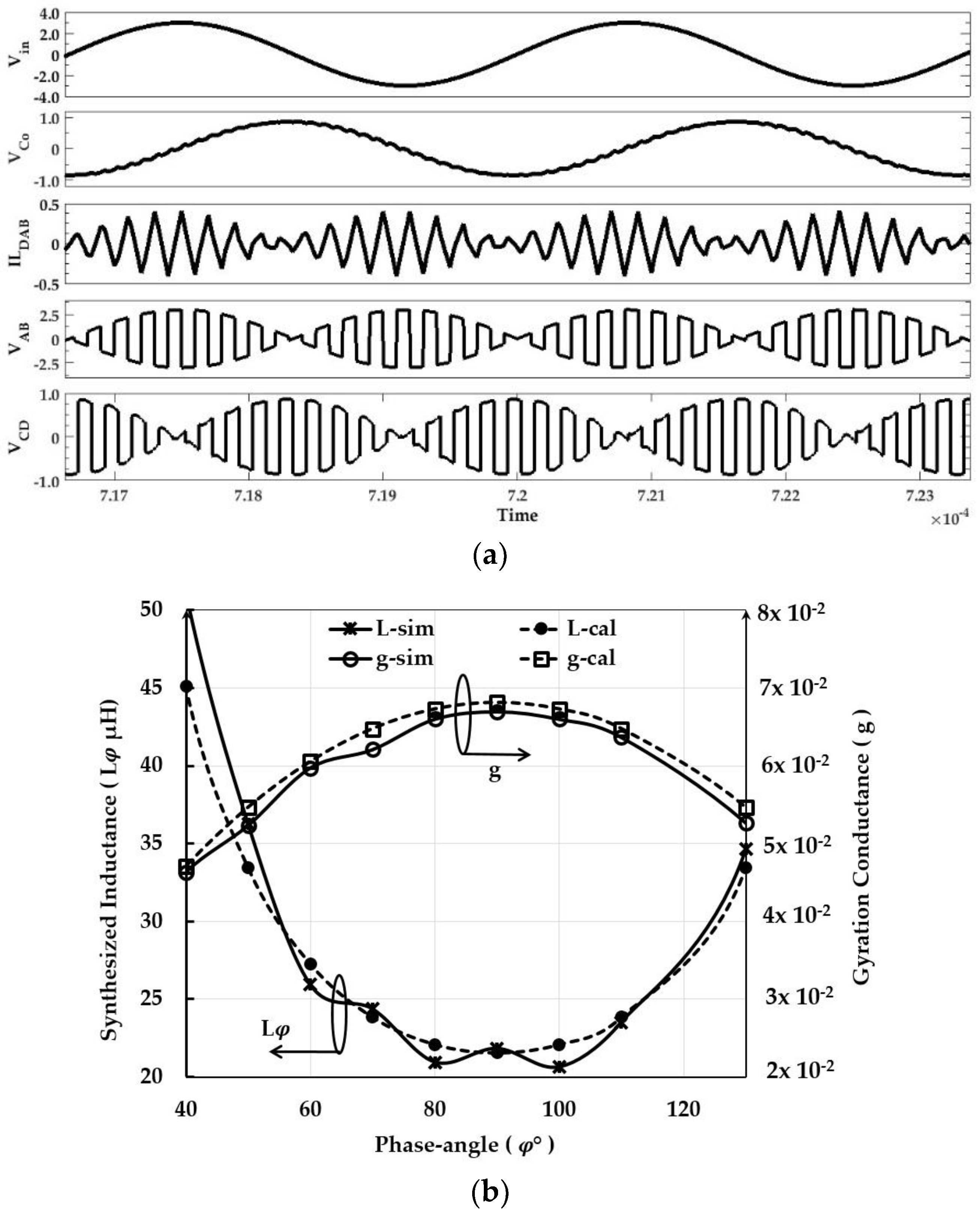
Figure 7.
Block diagram of the dynamic frequency tuning gyrator-based parallel WPT receiver.

Figure 8.
Block diagram of the Q-PLL control for gyrator-based dynamic frequency tuning system in Figure 7.
Figure 8.
Block diagram of the Q-PLL control for gyrator-based dynamic frequency tuning system in Figure 7.
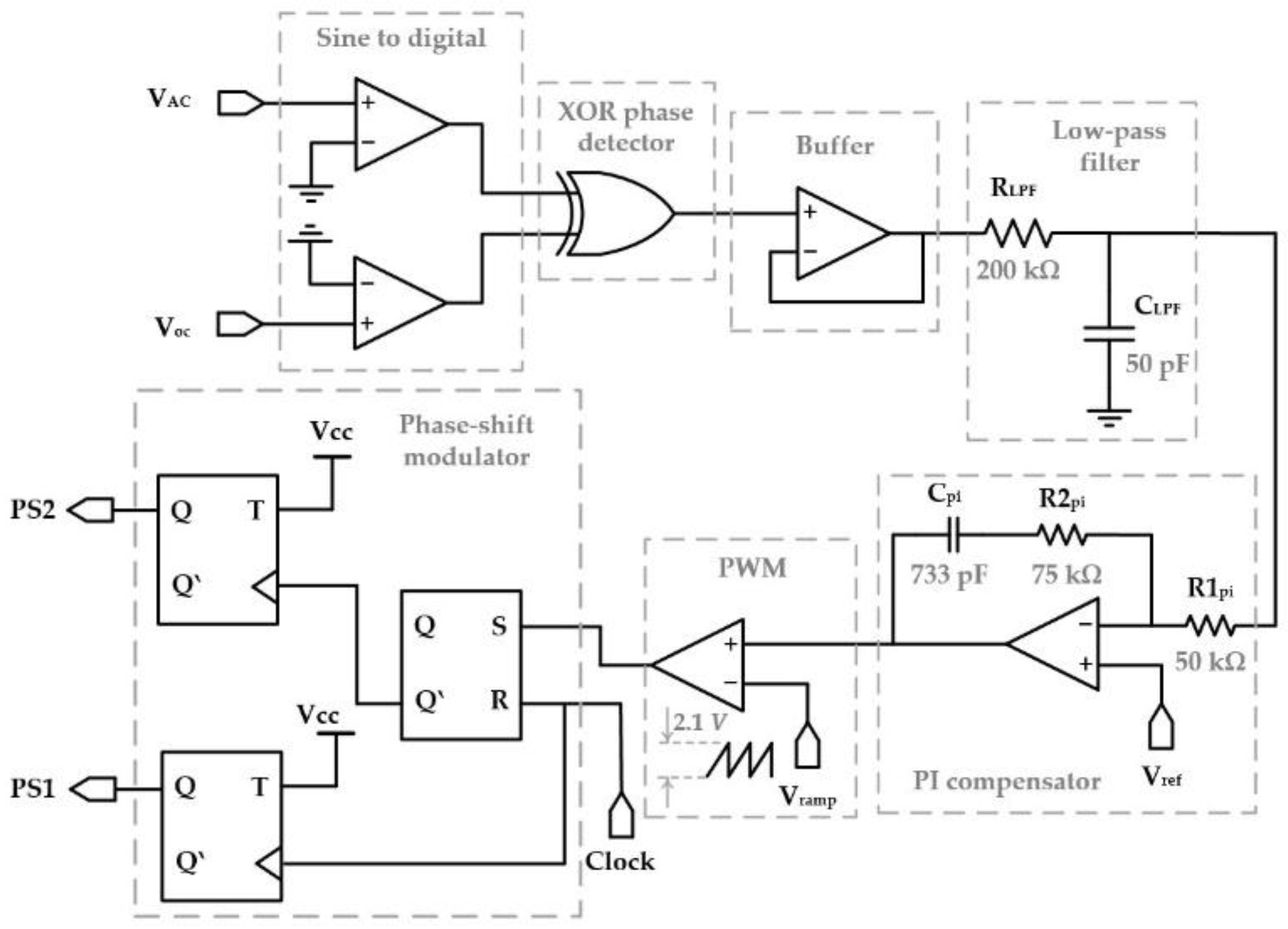
Figure 9.
System operation waveforms: (a) steady-state waveforms of VCtrl, VLPF and Vac; (b) a zoom-in showing the waveforms of QRL·Voc, Vac, Vramp, VCtrl, and DAB gating signals PS1 and PS2.
Figure 9.
System operation waveforms: (a) steady-state waveforms of VCtrl, VLPF and Vac; (b) a zoom-in showing the waveforms of QRL·Voc, Vac, Vramp, VCtrl, and DAB gating signals PS1 and PS2.

Figure 10.
System response to component variations showing Vac, VLPF and the phase-angle φ: (a) Case of −11% variation in CR followed by −11% variation in LR; (b) Case of +11% variation in CR followed by +11% variation in LR.
Figure 10.
System response to component variations showing Vac, VLPF and the phase-angle φ: (a) Case of −11% variation in CR followed by −11% variation in LR; (b) Case of +11% variation in CR followed by +11% variation in LR.
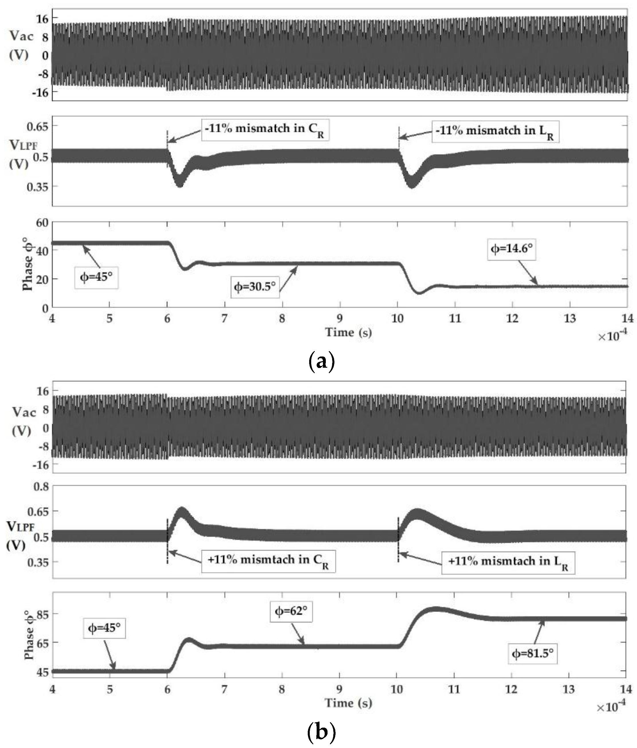
Figure 11.
Waveforms of system response to irregular change in CR and LR.

Figure 12.
Demonstration of system performance versus CR mismatch of ±15%: (a) Normalized delivered power with dynamic tuning (Po w/G) and without (Po w/o G); (b) The synthesized inductance Lφ, the corresponding φ and Vac versus CR mismatch.
Figure 12.
Demonstration of system performance versus CR mismatch of ±15%: (a) Normalized delivered power with dynamic tuning (Po w/G) and without (Po w/o G); (b) The synthesized inductance Lφ, the corresponding φ and Vac versus CR mismatch.

Figure 13.
Schematic diagram for on chip implementation for gyrator-based dynamic tuning.
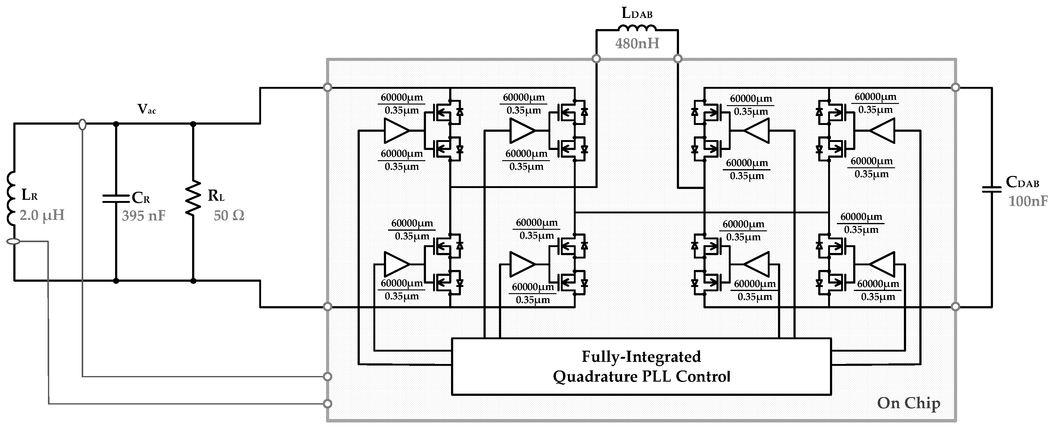
Figure 14.
Real-time chip design results: (a) tuned point steady-state waveforms of Vac, Voc and VPD; (b) the corresponding duty-cycle generated and driving signals for DAB circuit; (c) output power versus variations in CR and LR as well as the WPT receiver efficiency ηR based on real-time simulated chip implementation.
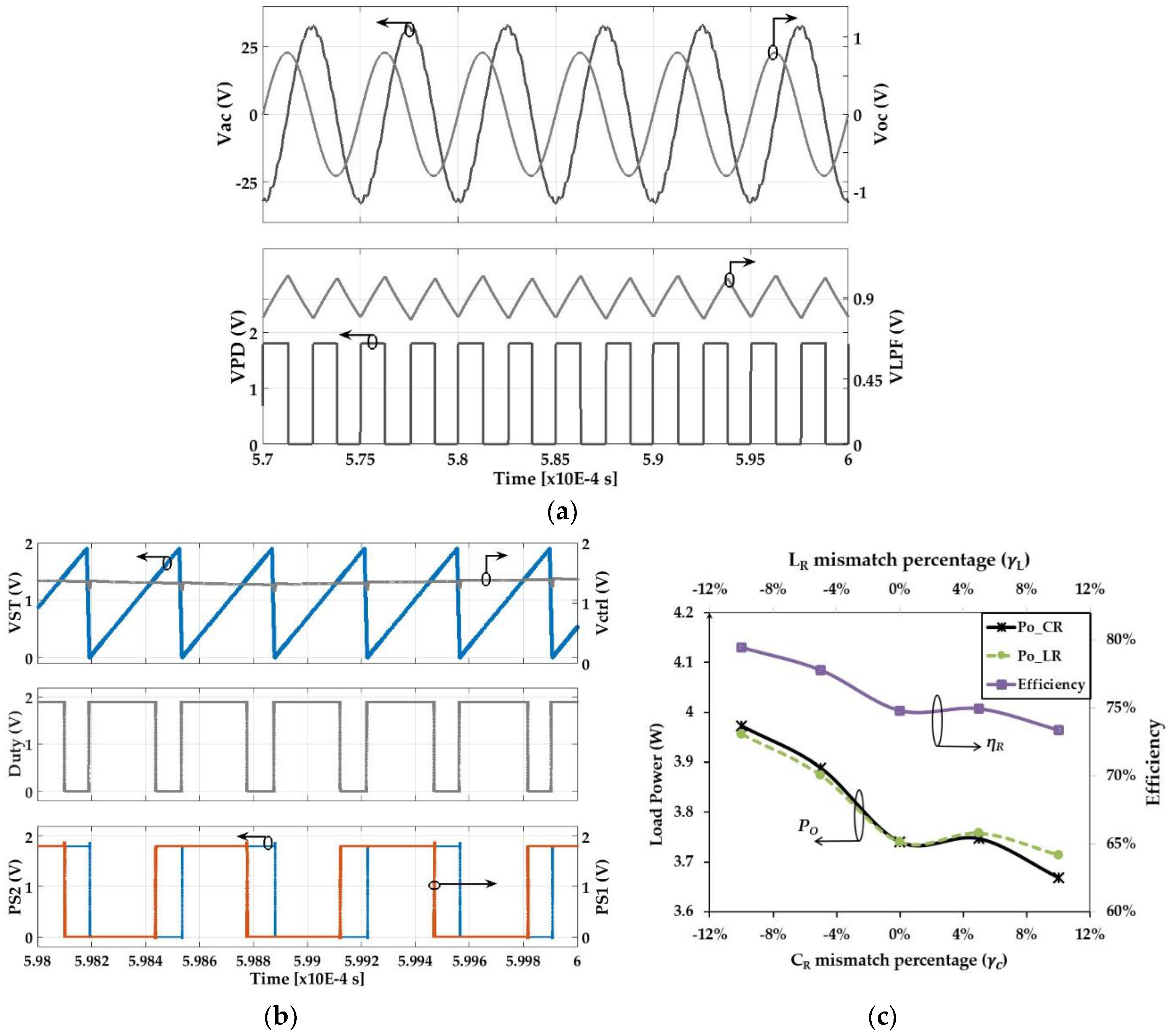
Figure 15.
Receiver circuit with parasitic resistances included and the Norton equivalent of circuit.
Figure 15.
Receiver circuit with parasitic resistances included and the Norton equivalent of circuit.
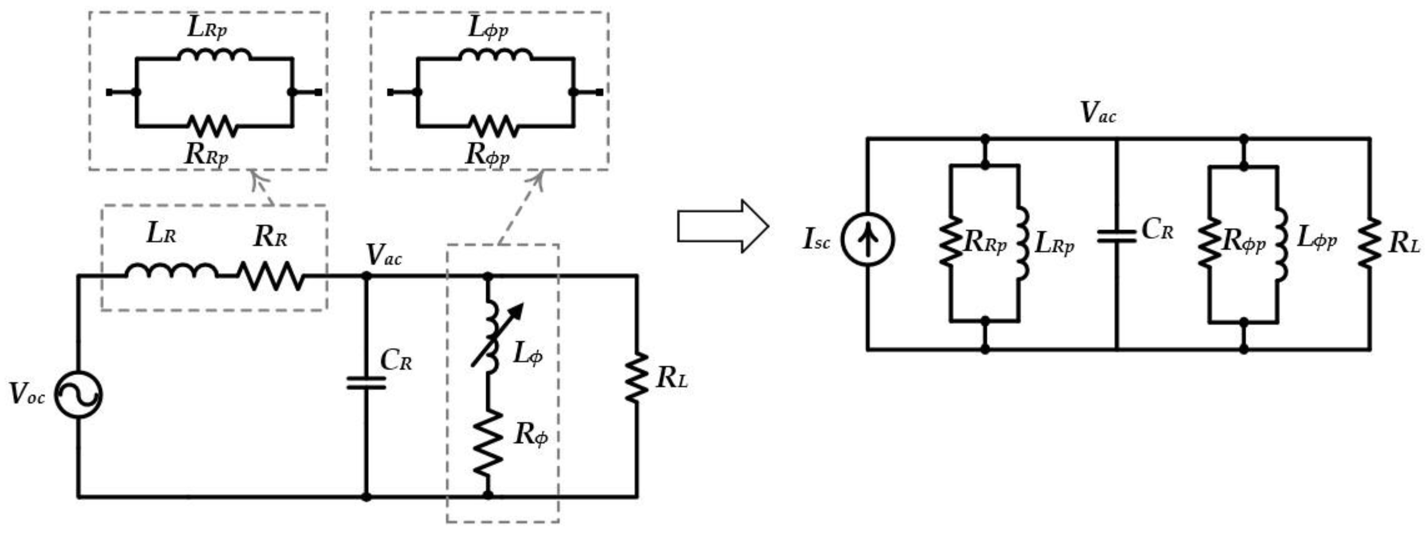
Figure 16.
Simplified block diagram for the closed-loop control.


Table 1.
Dual active bridge (DAB) circuit parameters.
| Parameter | fT | fDAB | LDAB | CDAB |
|---|---|---|---|---|
| Value | 300 kHz | 5 MHz | 367 nH | 100 nF |
Table 2.
System parameters. WPT: wireless power transfer.
| Parameter | Value |
|---|---|
| WPT link parameters | |
| Vin | 2.12 Vrms |
| fT | 200 kHz |
| LT | 10 μH |
| CT | 63.97 nF |
| M | 447.2 nF (k ≈ 0.1) |
| LR | 2.0 μH |
| CR | 395 nF |
| RL | 200 Ω (nominal) |
| DAB gyrator parameters | |
| fDAB | 1.5 MHz |
| LDAB | 480 nF |
| CDAB | 100 nF |
| Bidirectional-switch RON | 4 mΩ |
| φ | 45° (nominal) |
© 2018 by the authors. Licensee MDPI, Basel, Switzerland. This article is an open access article distributed under the terms and conditions of the Creative Commons Attribution (CC BY) license (http://creativecommons.org/licenses/by/4.0/).
Share and Cite
MDPI and ACS Style
Saad, M.; Alarcón, E. Insights into Dynamic Tuning of Magnetic-Resonant Wireless Power Transfer Receivers Based on Switch-Mode Gyrators. Energies 2018, 11, 453. https://doi.org/10.3390/en11020453
AMA Style
Saad M, Alarcón E. Insights into Dynamic Tuning of Magnetic-Resonant Wireless Power Transfer Receivers Based on Switch-Mode Gyrators. Energies. 2018; 11(2):453. https://doi.org/10.3390/en11020453
Chicago/Turabian StyleSaad, Mohamed, and Eduard Alarcón. 2018. "Insights into Dynamic Tuning of Magnetic-Resonant Wireless Power Transfer Receivers Based on Switch-Mode Gyrators" Energies 11, no. 2: 453. https://doi.org/10.3390/en11020453
Note that from the first issue of 2016, this journal uses article numbers instead of page numbers. See further details here.