Article

Design of Peak Efficiency of 85.3% WPC/PMA Wireless Power Receiver Using Synchronous Active Rectifier and Multi Feedback Low-Dropout Regulator

1
College of Information and Communication Engineering, Sungkyunkwan University, Suwon 16419, Korea
2
School of Information and Communications, Gwangju Institute of Science and Technology, Gwangju 61005, Korea
*
Author to whom correspondence should be addressed.
Energies 2018, 11(3), 479; https://doi.org/10.3390/en11030479
Submission received: 20 January 2018 / Revised: 12 February 2018 / Accepted: 22 February 2018 / Published: 25 February 2018

Abstract

:
An efficient synchronous active rectifier and Multi Feedback low drop out (LDO) Regulator coupled with a wireless power receiver (WPR) is proposed in this study. An active rectifier with maximum power conversion efficiency (PCE) of 94.2% is proposed to mitigate the reverse leakage current using zero current sensing. Output voltage and current are regulated by multi-feedback LDO regulator, sharing the single path transistor. The proposed chip is fabricated in the 0.18 μm BCD technology having die area of 16.0 mm2. A 94.2% power conversion efficiency with the load current of 800 mA is measured for the proposed active rectifier.

1. Introduction

Wireless power transfer (WPT) technology is getting significant attention in recent research, especially with mobile phone chargers. Its applications vary from medical components to automobiles [1]. The inductive coupling method is one of the popular WPT methods applicable for a distance below 0.5 cm with a transfer frequency in the range of 87 kHz to 375 kHz. This method is standardized by two consortiums: Wireless Power Consortium (WPC) and the Power Matters Alliance (PMA). Whatever we use the charging technique for, maintaining a high efficiency is necessary which is important because low efficiency will produce heat from the receiver which creates several problems. Under normal conditions, a WPT system has more than 5 W of power at its input, low efficiency of the receiver causes heat which reduces the receiver efficiency [2,3,4,5,6]. Usually, the whole efficiency of wireless power receiver (WPR) is controlled by the rectifier [7]. As low-dropout (LDO) regulators get their DC supply from the rectifier, rectifier efficiency is crucial. The output voltage of rectifier determines the LDO regulator’s efficiency. Protection functions like over current protection (OCP), over voltage protection (OVP), and adaptive communication limit (ACL) are unified with the LDO regulator.
This study proposes an efficient active rectifier and multi-feedback LDO (MF-LDO) regulator coupled with a wireless power receiver. Section 2 describes the architecture and building blocks of inductive coupling WPR. The simulation results are presented in Section 3 and Section 4 summarizes the paper.

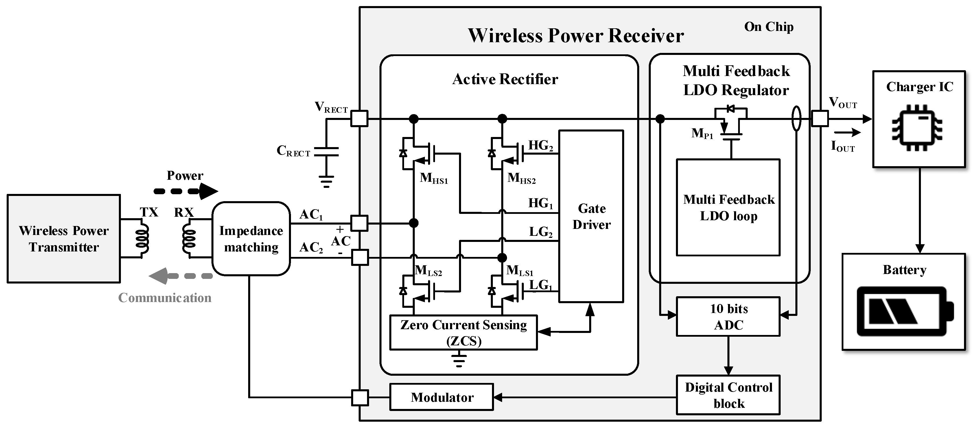
2. Proposed Wireless Power Receiver Design and Its Implementation

2.1. Architecture

The simplified block diagram of the wireless power receiver is depicted in Figure 1 where the power is transmitted to the receiver through the coil. The impedance matching network maximizes the power transfer from the receiving coil to active rectifier. The active rectifier converts the input AC signals (AC1 and AC2) to DC voltage. The proposed active rectifier uses synchronous control by tracking input frequency by ZCS (zero current sensing) with a monostable circuit to eliminate the double pulse problem. The battery needs regulated DC voltage which is generated by the MF-LDO regulator. Protection functions are integrated to the proposed MF-LDO in this work. A 10-bit ADC converts the internal analog signals from several blocks into digital signals. The digital control block collects them and arranges the packets based on them. To perform the load modulation, it serializes the parallel data into serial data and finally delivers to the modulator. In this work, a complete wireless power receiver (WPR) is designed with proposed active rectifier and MF-LDO.

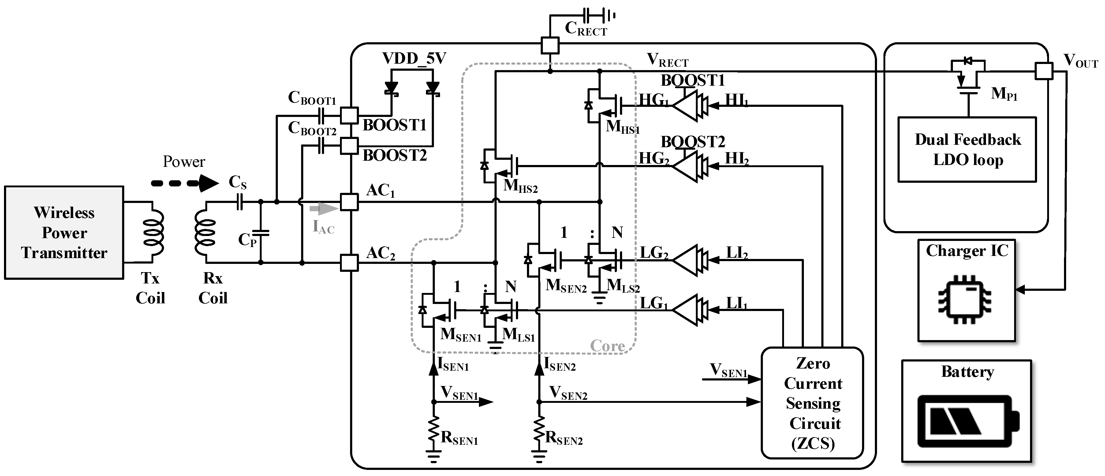
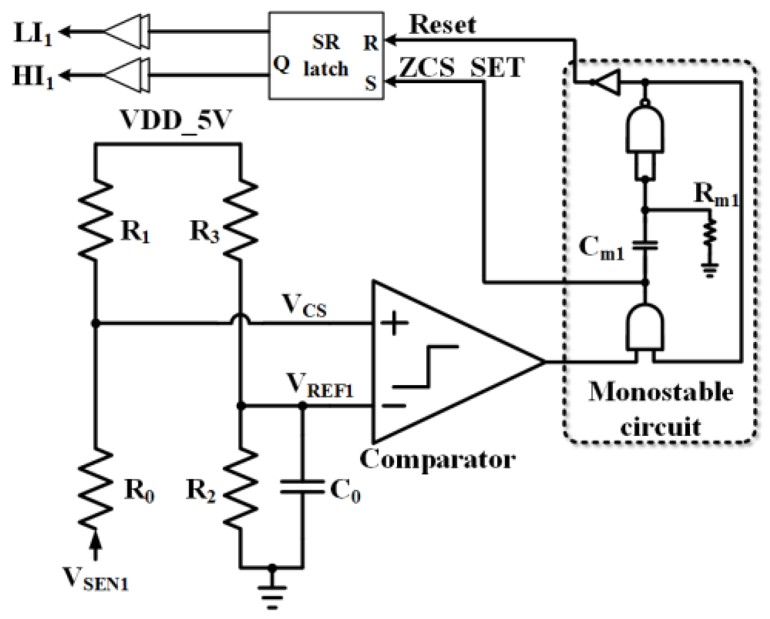
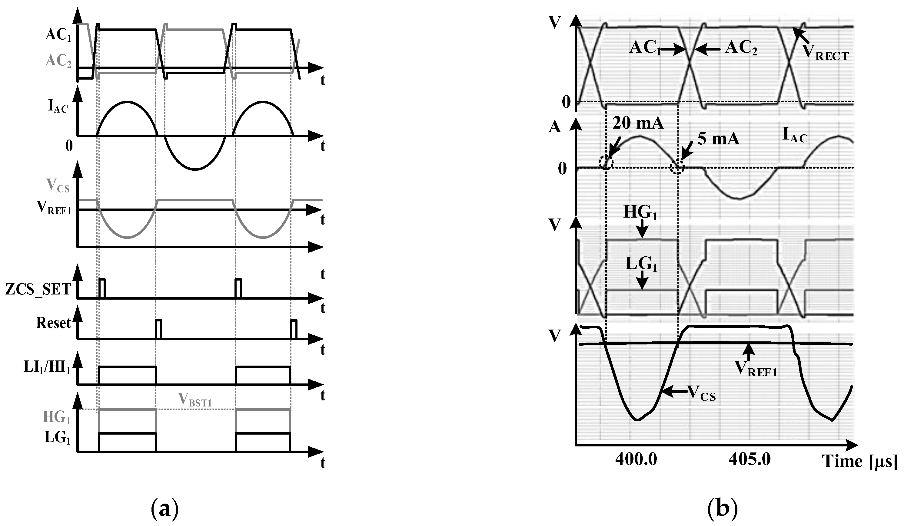
2.2. Active Rectifier

A design of active rectifier is proposed in this work which receives AC input voltage, the polarity of this input voltage decides which metal oxide semiconductor (MOS) transistor will turn on and off actively in the active rectifier, as exhibited in Figure 2. High power conversion efficiency is achieved because, at MOS transistors, less voltage drop can be made as compared to diode-based passive rectifier [8].
η rectifier = V out | V in | × I out I in V out V do + V out × I out I loss + I out
The rectifier efficiency is calculated by Equation (1).
In this equation;
Vdo = Voltage drop in conducting path
Iloss = Current loss, defined by the reverse current leakage in power stage
As the power transfer begins, the active rectifier operates in passive mode and operates in active mode when VRECT gets voltage of the required power level.
The received AC power input rectification power conversion efficiency will be low with high output power level, therefore, the power efficiency of the rectifier is maximized by minimizing Vdo [9]. Passive diodes have some forward voltage drop which can limit the efficiency of a rectifier [8,10,11].
On the other hand, MOS transistors have a bidirectional current flow where current flow will be from DC output to AC input. Power conversion efficiency is extremely reduced by this leakage current [12,13,14,15,16].
In Figure 3, the ZCS circuit senses the current of the active rectifier to prevent the reverse leakage current. To generate the gate signals (LI1, HI1) that turn on and off MLS1 and MHS1 respectively, the ZCS circuit senses source voltages (VSEN1) of the sensing MOSFET (MSEN1). Also, gate control signals of LI2 and HI2 are generated by MSEN2 in the same way. The gate control signals (LI1, HI1) are turned and off based on Equations (2) and (3).
Turn - on : V REF 1 ( VDD _ 5 V V SEN 1 ) × R 0 R 1 + R 0
Turn - off : V REF 1 > ( VDD _ 5 V V SEN 1 ) × R 0 R 1 + R 0
The efficiency of the active rectifier is improved by the ZCS circuits because reverse currents of the active rectifier are prevented. The resistors of R0, R1, R2, and R3 with a low-temperature variation are used in ZCS circuit. The VREF1 and VCS voltages are generated by resistive ratio. Therefore, the ZCS circuit is designed strongly against the change in PVT variation. The monostable circuit and SR latch in the ZCS circuits are used to prevent the double pulse problem by glitches in the gate signals (LI1,2 and HI1,2).
The timing diagram of the ZCS circuit is shown in Figure 4a. At zero crossing point of ZCS_SET is generated. In Figure 2, power transistors (MHS1, MHS2, MLS1, and MLS2) are turned on by ZCS_SET and turned off by the reset signal. To turn on the high side transistors (MHS1 and MHS2) with the minimum conduction losses, the bootstrap circuit shown in Figure 2 generates boost voltages (VBST1 and VBST2) with the amplitude levels of AC signals (AC1 and AC2) plus 5 V since the maximum gate-source voltages of high side transistors (MHS1 and MHS2) are 5 V in this process.
The simulation results of the Active rectifier are shown Figure 4b. When IAC is 20 mA, the LG1 and HG1 are turned on. On the other hand, when the IAC is less than 5 mA, LG1, and HG1 are turned off and the reverse leakage current is blocked.

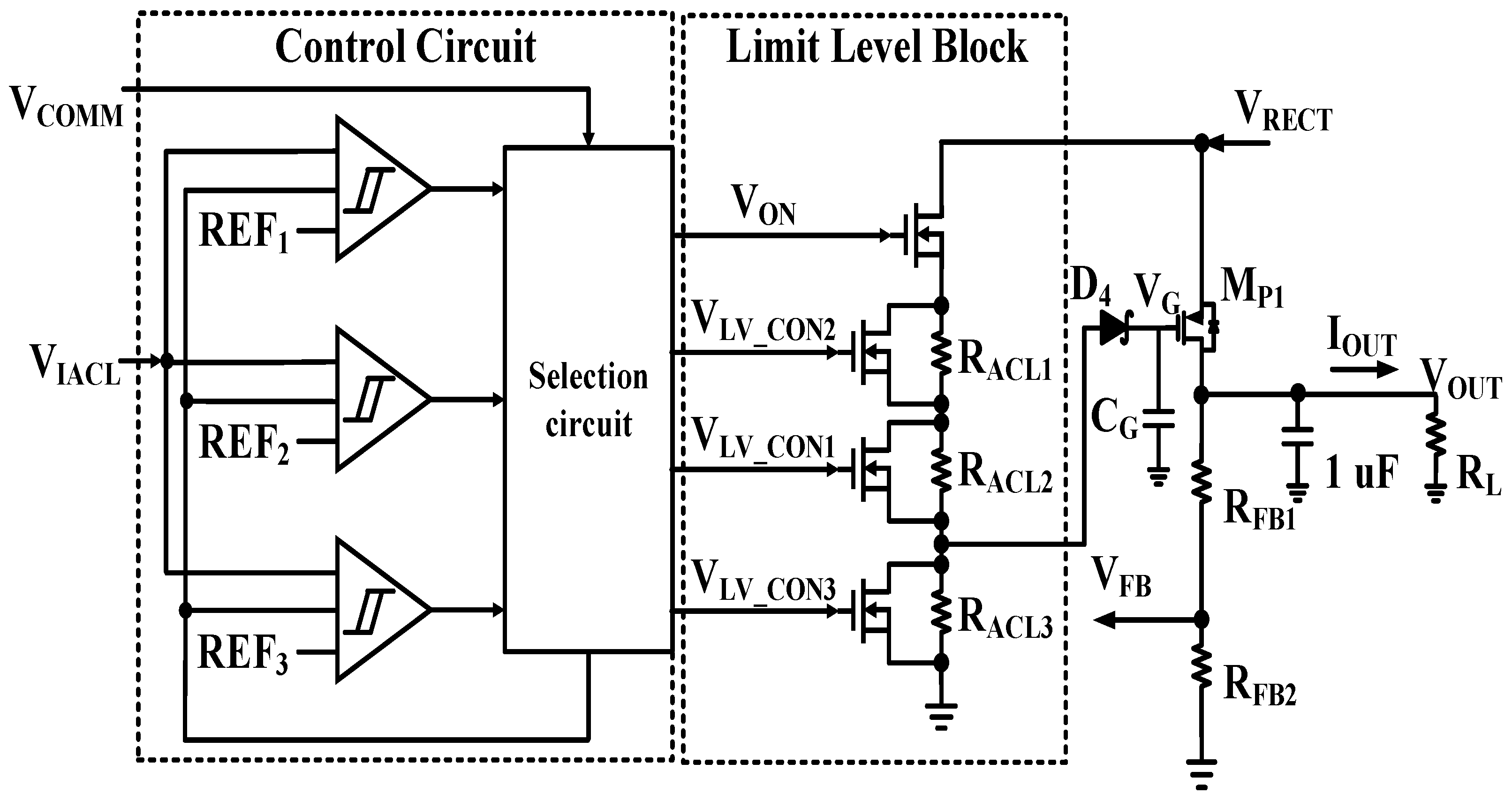
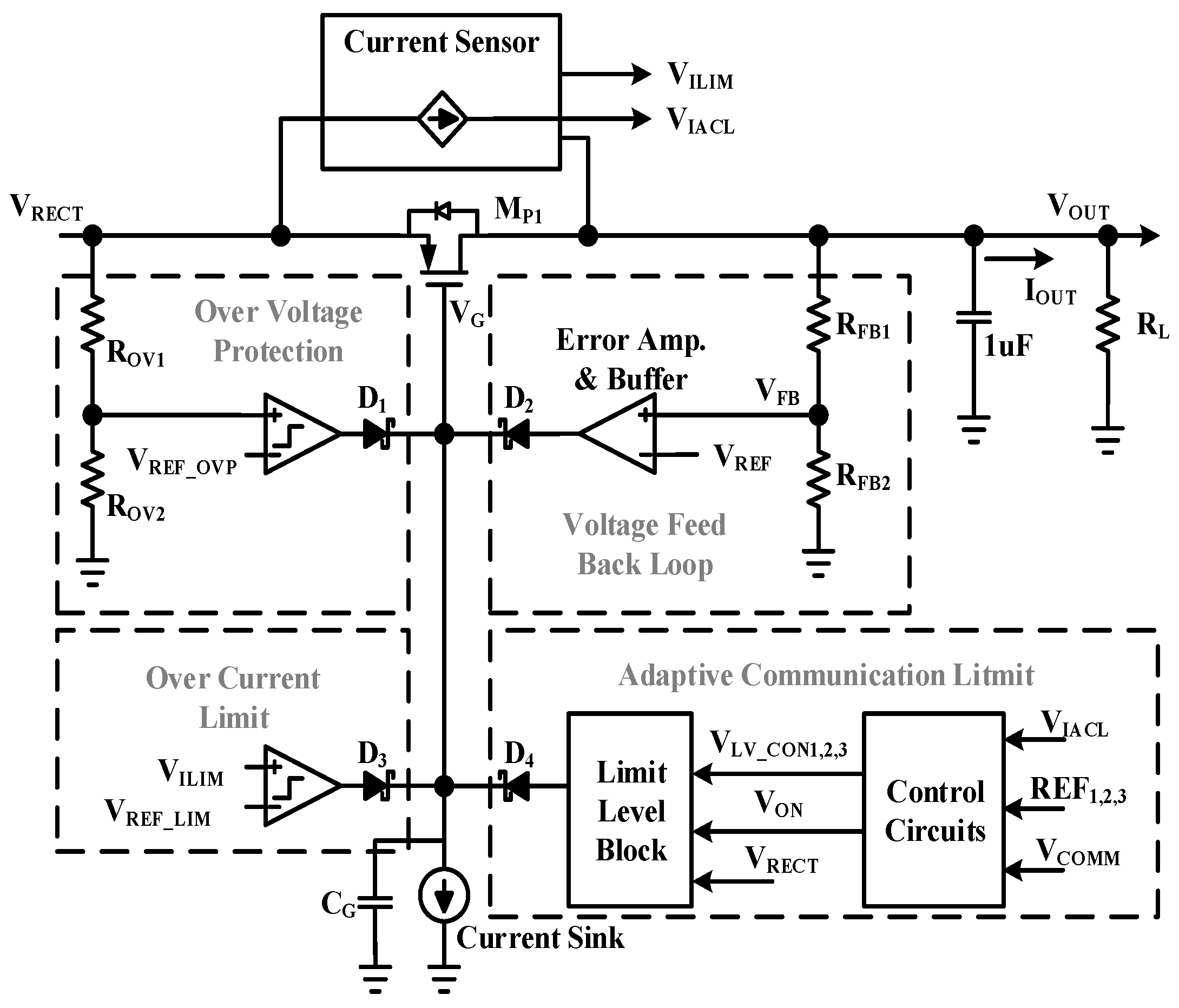
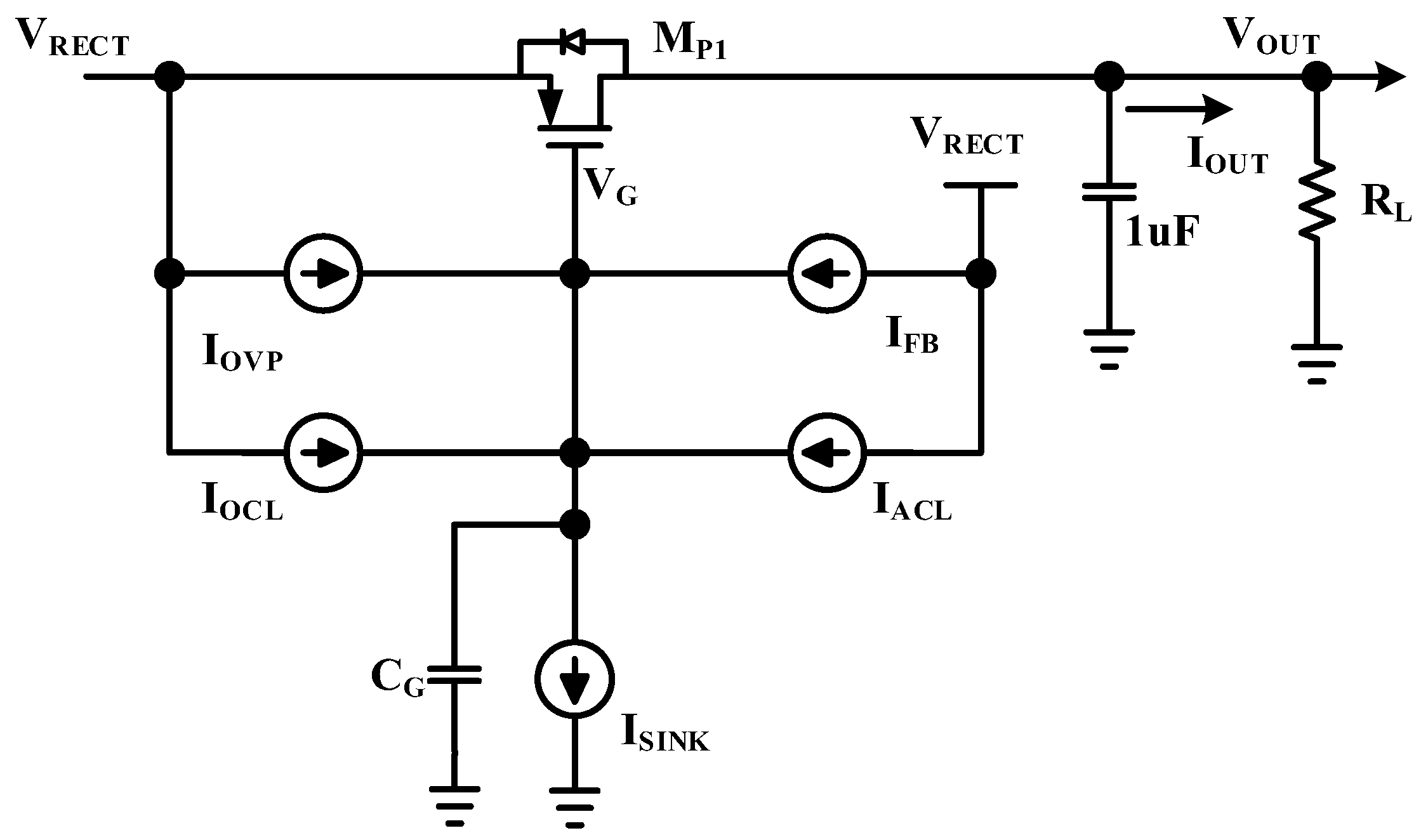
2.3. Multi Feedback LDO (MF-LDO) Regulator

A regulated DC output is provided to the charger IC before the battery and this is provided by the LDO regulator. In the WPR system, the receiver needs various protection functions. In a conventional LDO regulator, the voltage feedback loop is implemented. A MF-LDO regulator is proposed in Figure 5, in which the protection functions are incorporated to low-dropout regulator. The MF-LDO regulator shares the power transistor MP1, to save die area.
Figure 6 shows simplified functional diagram of multi feedback LDO. The load current, IOUT, is defined by VG, VRECT, and VOUT voltages. VOUT and VRECT voltages are defined by the specification and the active rectifier respectively. Therefore, only VG controls the IOUT, and is derived from Equation (4).
V G = t C G × ( I FB + I OVP + I OCL + I ACL + I SIN K )
In the normal operation mode of MF-LDO, the ISINK current discharges the VG node constantly. Also, the IFB current is generated by voltage feedback loop. Therefore, VOUT voltage is regulated constantly, and the VG voltage is changed depending on IOUT currents. In the protection modes of MF-LDO—such as OCP, OVP, or ACL modes—IOCP, IOVP, and IACL are not zero current sources. When the IOCP, IOVP, and IACL are not zero current sources, VG voltage is increased and the IOUT current is blocked or limited since the ISINK current is constant.
Figure 7 shows the adaptive communication limit (ACL) circuit. If the load current (IOUT) increases rapidly during the WPC communication period, communication errors may occur. In order to prevent it, IOUT is limited by the ACL circuit. The input signals of control circuits are the VCOMM signal, the output signal (VIACL) of the current sensor, and references (REF1,2,3). The ACL is enabled by the VCOMM signal and the current limit level is determined depending on the voltage level of VIACL signal. When the VON is high, the parasitic gate capacitor (CG) of MP1 is charged by the limit level block through the diode, D4. Therefore, the voltage level of VG is increased, and the output current (IOUT) is limited.
Simulated results of a MF-LDO regulator are presented in Figure 8. The MF-LDO regulator regulates the output voltage to 5 V under the load current of 200 mA. The ACL is enabled at this load current and regulated up to 400 mA.

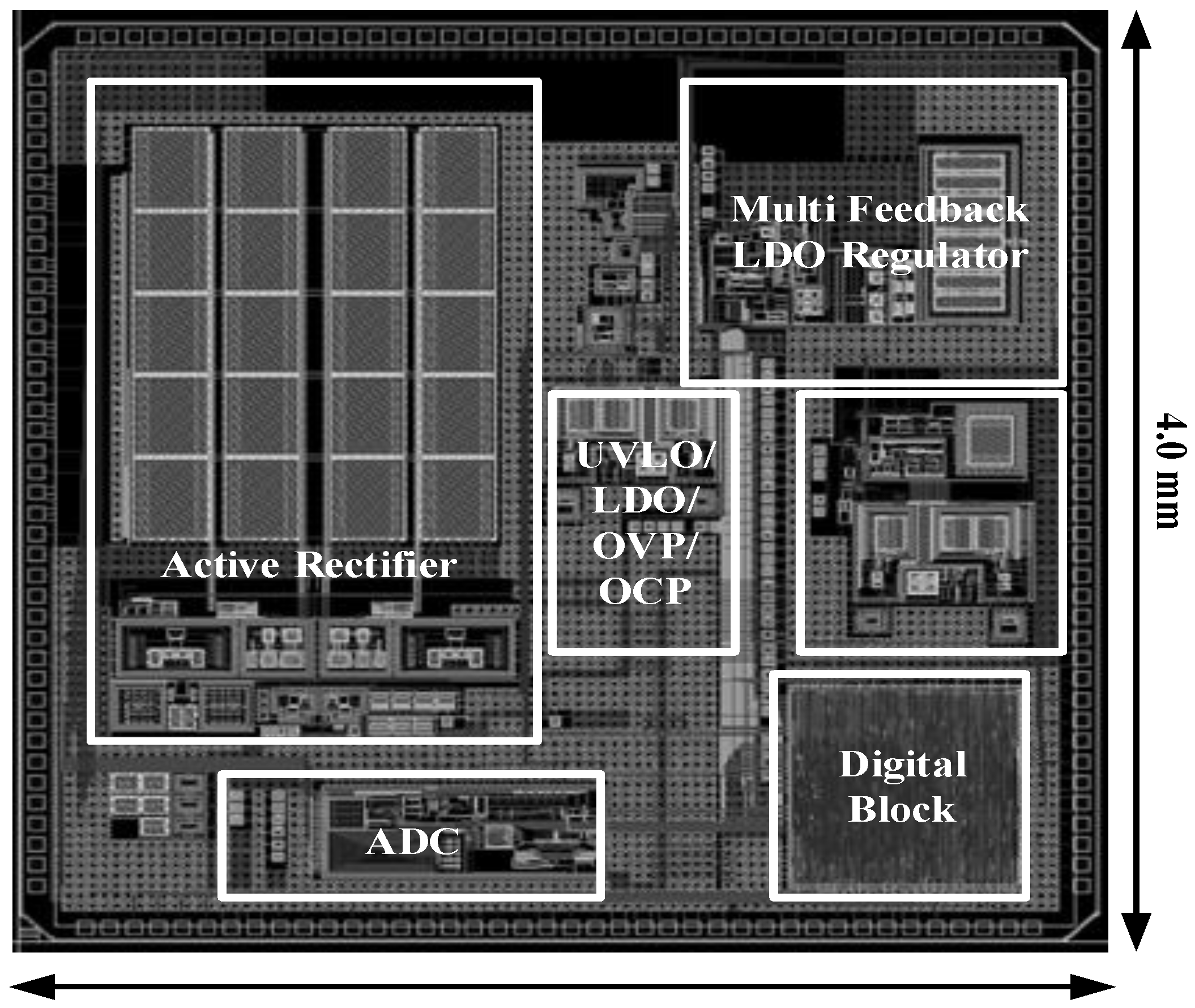
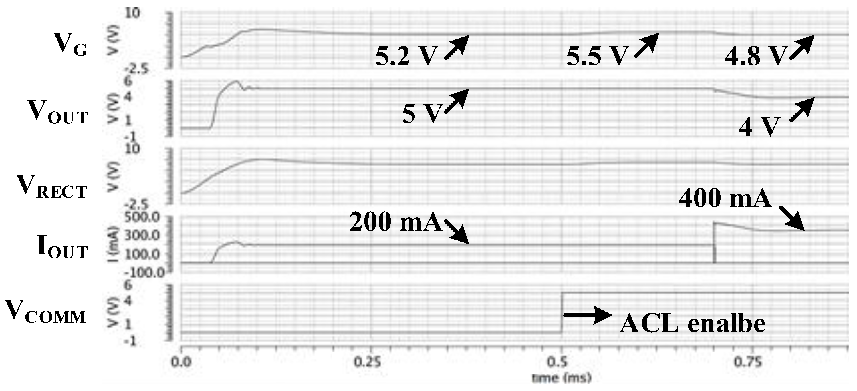
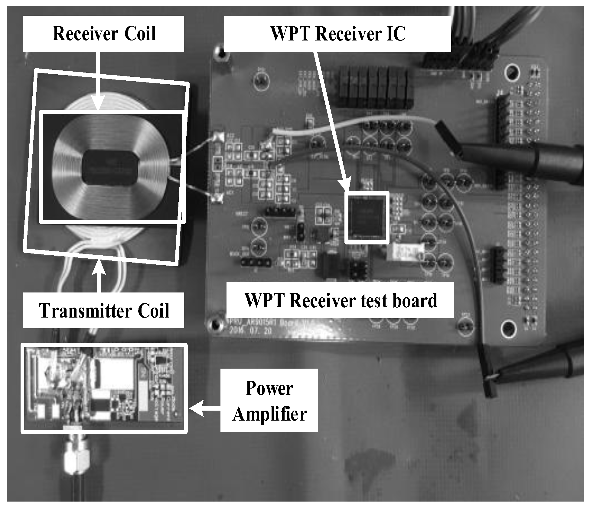
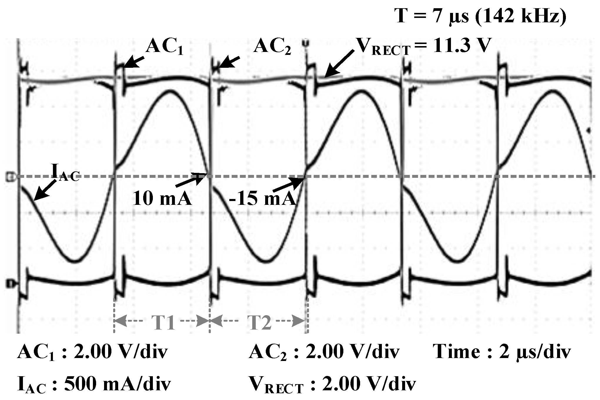
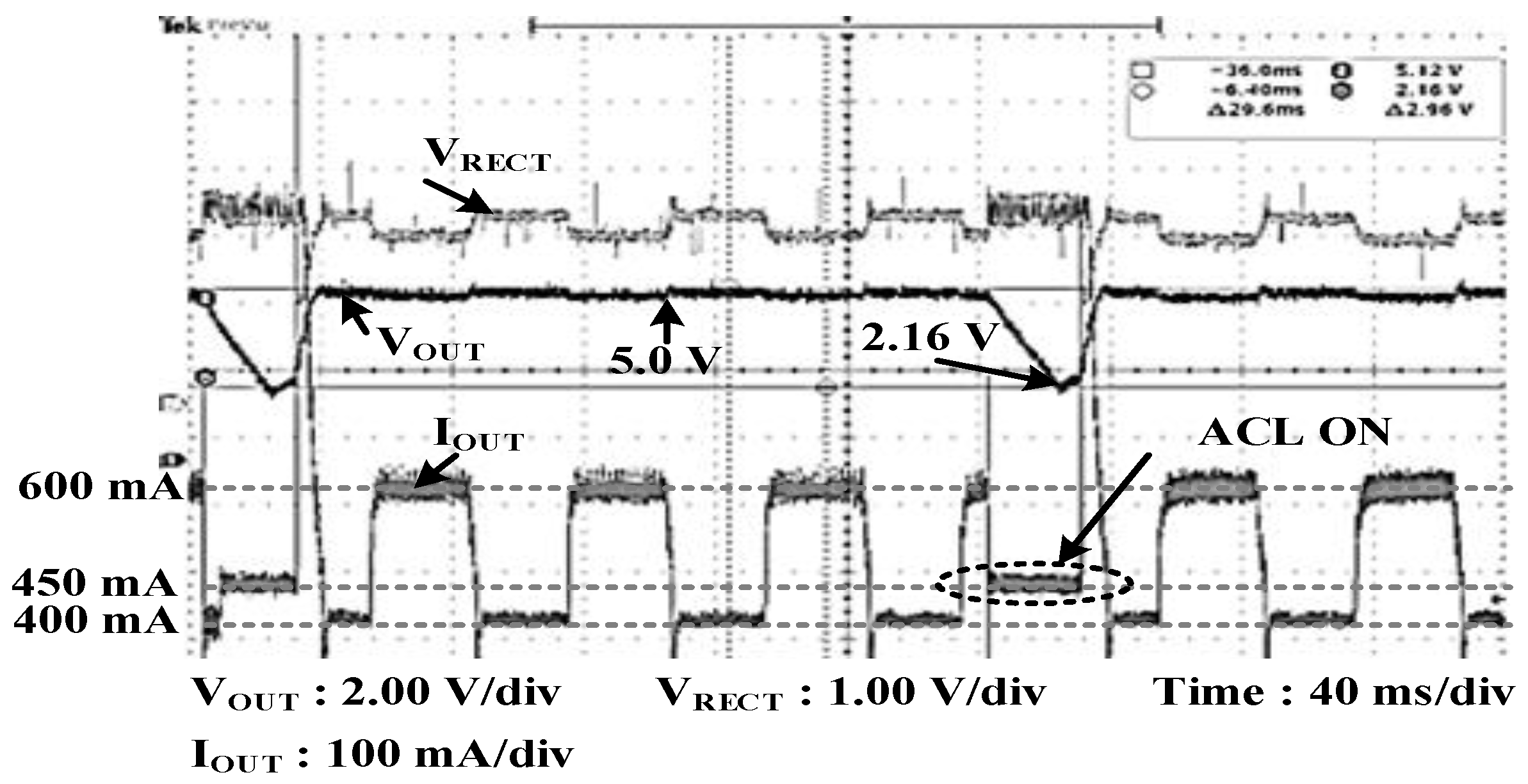
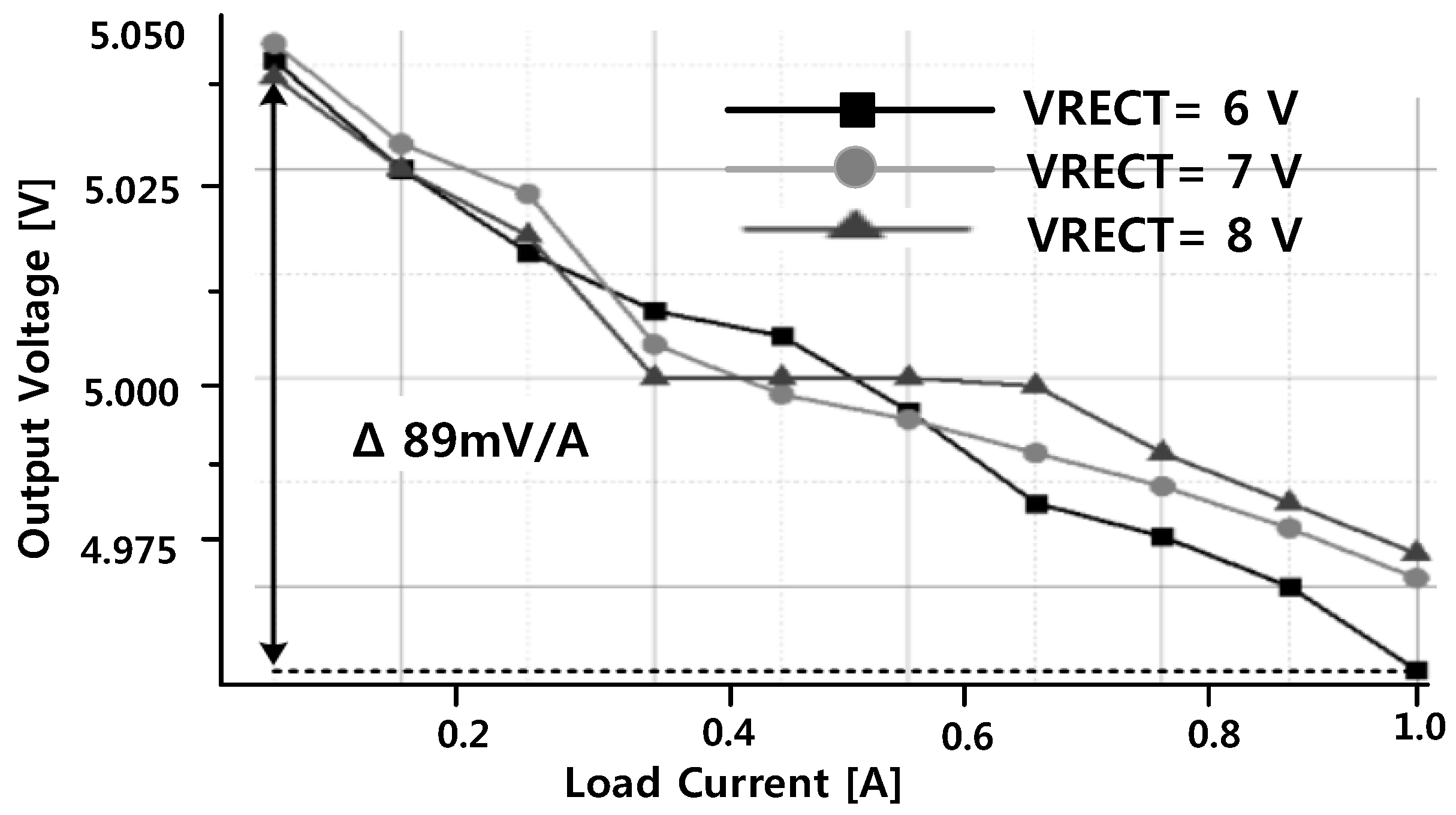
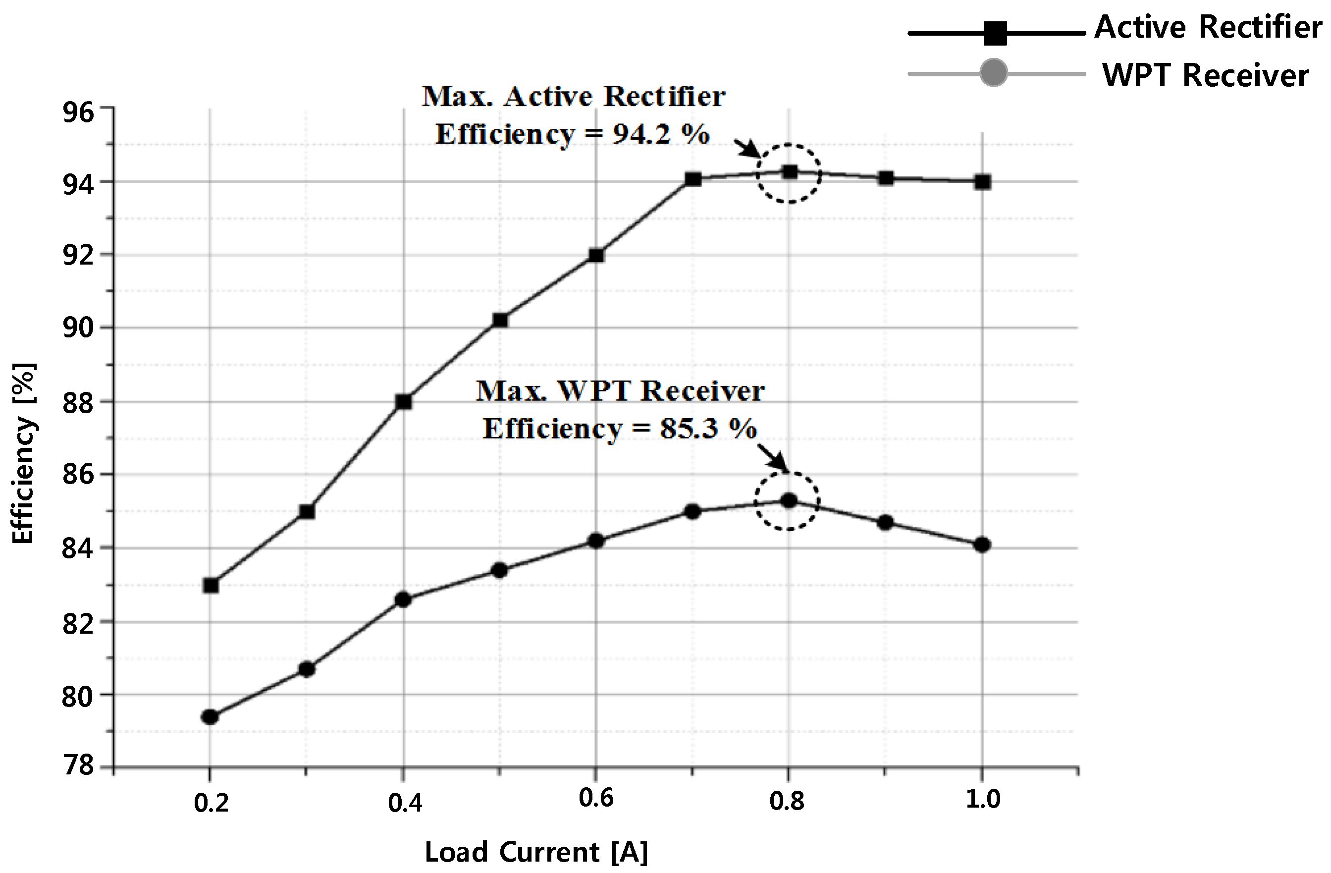
3. Experimental Results

The proposed WPR chip is fabricated in 0.18 µm 1P4M with MIM capacitors and high sheet resistance poly resistors. Figure 9 shows the chip layout pattern of the WPR. The die area in the WPR is 16.0 mm2.
The measurement environment of wireless power receiver is displayed in Figure 10. Inductive wireless power is generated by power transmitter. Below the receiver coil, a transmitter coil is placed.
The measured waveform of the active rectifier is revealed in Figure 11. The ZCS circuit operates the active rectifier. MHS1 and MLS1 start to be turned on at 10 mA current of IAC and are active during the interval time T1. On the other hand, MHS2 and MLS2 start to be turned on at −15 mA current of IAC and are active during the interval time T2.
The measured waveform of MF-LDO is shown in Figure 12. The value of load current (IOUT) varies from 200 mA to 600 mA to check the performance of MF-LDO. When the MF-LDO is in the normal operation mode, VOUT is regulated to 5.0 V. On the other hand, when the ACL is enabled, IOUT is limited to 450 mA.
In Figure 13, the rectifier output voltage (VRECT) can change from 6 V to 8 V, whereas the variation of MF-LDO output voltage (VOUT) is less than 89 mV/A. For this measurement, VRECT is provided from the power supply.
When the value of load current is 800 mA in Figure 14, the maximum measured PCE of the active rectifier and wireless power receiver are 94.2% and 85.3%, respectively.
The performance comparison with prior works is shown in Table 1 [8,17,18]. The examples from [8,17] are active rectifiers for A4WP standard operating at 6.78 MHz and their efficiencies are 91.5% and 94.2% respectively. The maximum efficiency of [18] is 92.7% when the input frequency is 150 kHz. Therefore, this work achieves an efficiency of 92.4% and has the best performance when the input frequency is 150 kHz. This work shows the highest overall efficiency of a rectifier compared with references.

4. Conclusions

This work describes an inductive coupling (WPC/PMA) WPR having high-efficiency Active rectifier and MF-LDO Regulator. The synchronous Active rectifier with ZCS is proposed to get high efficiency in order to reduce the reverse leakage current. MF-LDO Regulator is proposed to implement the output voltage regulation, OVP, over current limit (OCL), and ACL sharing the single power transistor.
This chip is implemented in the 0.18 μm BCD technology having die area of 16.0 mm2. The maximum PCE of the Active rectifier is 94.2% at 800 mA load current.

Acknowledgments

This work was supported by Institute for Information & Communications Technology Promotion (IITP) grant funded by the Korea government (MSIP) (No. B0717-16-0057, Development of MST integrated 15W magnetic induction/resonance wireless charging technology). This work was supported by the National Research Foundation of Korea (NRF) grant funded by the Korean government(MSIP) (2014R1A5A1011478).

Author Contributions

Kang-Yoon Lee guided and directed the autors for this work. Zaffar Hayat Nawaz Khan and Young-Jun Park studied, proposed and designed the overall architecture of synchronous active rectifier and Multi Feedback low drop out (LDO) Regulator coupled with a wireless power receiver. They wrote the paper. Byeong Gi Jang, Seong-Mun Park and Hamed Abbasizadeh contributed in making the layout of the proposed architecture. Keum Cheol Hwang guided the antenna and measurments. Young Gun Pu performed the measurements with Zaffar, Young-Jun Park and Seong Jin Oh. Youngoo Yang and Minjae Lee designed the related top architecture.

Conflicts of Interest

The authors declare no conflict of interest.

References

  1. Wireless Power Consortium System. Description Wireless Power Transfer, Vol. I: Low Power, Part 1: Interface Definition Version 1.0. July 2010. Available online: https://www.wirelesspowerconsortium.com (accessed on 23 February 2018).
  2. Kiani, M.; Lee, B.; Yeon, P.; Ghovanloo, M. A Q-modulation technique for efficient inductive power transmission. IEEE J. Solid-State Circuits 2015, 50, 2839–2848. [Google Scholar] [CrossRef] [PubMed]
  3. Choi, J.-H.; Yeo, S.-K.; Park, S.; Lee, J.-S.; Cho, G.-H. Resonant regulating rectifiers (3R) operating for 6.78 MHz resonant wireless power transfer (RWPT). IEEE J. Solid-State Circuits 2013, 48, 2989–3001. [Google Scholar] [CrossRef]
  4. Moh, K.-G.; Neri, F.; Moon, S.; Yeon, P.; Yu, J.; Cheon, Y.; Roh, Y.; Ko, M.; Park, B.-H. A fully integrated 6W wireless power receiver operating at 6.78MHz with magnetic resonance coupling. In Proceedings of the 2015 IEEE International Solid-State Circuits Conference, San Francisco, CA, USA, 22–26 February 2015; IEEE: Piscataway, NJ, USA, 2015; pp. 230–231. [Google Scholar]
  5. Cheng, L.; Ki, W.H.; Tsui, C.Y. A 6.78-MHz single-stage wireless power receiver with a 3-mode reconfigurable resonant regulating rectifier. IEEE J. Solid-State Circuits 2017, 52, 1412–1423. [Google Scholar] [CrossRef]
  6. Koh, K.; Beh, T.; Imura, T.; Hori, Y. Impedance Matching and Power Division Using Impedance Inverter for Wireless Power Transfer via Magnetic Resonant Coupling. IEEE Trans. Ind. Appl. 2013, 50, 2061–2070. [Google Scholar] [CrossRef]
  7. Hashemi, S.; Sawan, M.; Savania, Y. A Novel Fully-Integrated Drop Less Voltage CMOS Rectifier for Wireless Powered Devices. In Proceedings of the 2007 Internatonal Conference on Microelectronics, Cairo, Egypt, 29–31 December 2007; pp. 333–336. [Google Scholar]
  8. Park, H.-G.; Jang, J.-H.; Kim, H.-J.; Park, Y.-J.; Oh, S.J.; Pu, Y.G.; Hwang, K.C.; Yang, Y.; Lee, K.-Y. A Design of a Wireless Power Receiving Unit With a High-Efficiency 6.78-MHz Active Rectifier Using Shared DLLs for Magnetic-Resonant A4 WP Applications. IEEE Trans. Power Electron. 2016, 31, 4484–4498. [Google Scholar] [CrossRef]
  9. Guo, S.; Lee, H. An Efficiency-Enhanced CMOS Rectifier With Unbalanced-Biased Comparators for Transcutaneous-Powered High-Current Implants. IEEE J. Solid-State Circuits 2009, 44, 1796–7804. [Google Scholar] [CrossRef]
  10. Lee, H.-M.; Ghovanloo, M. An Adaptive Reconfigurable Active Voltage Doubler/Rectifier for Extended-Range Inductive Power Transmission. IEEE Trans. Circuits Syst. II Express Briefs 2012, 59, 481–485. [Google Scholar] [CrossRef]
  11. Lu, Y.; Ki, W.-H. A 13.56 MHz CMOS Active Rectifier with Switched-Offset and Compensated Biasing for Biomedical Wireless Power Transfer Systems. IEEE Trans. Biomed. Circuits Syst. 2013, 8, 334–344. [Google Scholar]
  12. Cheng, L.; Ki, W.H.; Lu, Y.; Yim, T.S. Adaptive on/off delay-compensated active rectifiers for wireless power transfer systems. IEEE J. Solid-State Circuits 2016, 51, 712–723. [Google Scholar]
  13. Lam, Y.-H.; Ki, W.-H.; Tsui, C.-Y. Integrated Low-Loss CMOS Active Rectifier for Wirelessly Powered Devices. IEEE Trans. Circuits Syst. II: Express Briefs 2006, 53, 1378–1382. [Google Scholar] [CrossRef]
  14. Tseng, R.; Novak, B.; Shevde, S.; Grajski, K.A. Introduction to the alliance for wireless power loosely-coupled wireless power transfer system specification version 1.0. In Proceedings of the 2013 IEEE Wireless Power Transfer (WPT), Perugia, Italy, 15–16 May 2013; pp. 79–83. [Google Scholar]
  15. Park, Y.-J.; Oh, S.J.; Kim, S.Y.; Cho, S.; Kim, M.C.; Park, J.-H.; Lee, D.S.; Kim, H.J.; Lee, K.-Y. A Design of Inductive Coupling Wireless Power Receiver with High-Efficiency Active Rectifier and Multi Feedback LDO Regulator. In Proceedings of the 2016 IEEE Wireless Power Transfer Conference (WPTC), Aveiro, Portugal, 5–6 May 2016. [Google Scholar]
  16. Shinohara, H.; Miyaji, K. A ZVS CMOS active diode rectifier with voltage-time-conversion delay-locked loop for wireless power transmission. In Proceedings of the 2015 IEEE Asian Solid-State Circuits Conference (A-SSCC), Xiamen, China, 9–11 November 2015; pp. 3–15. [Google Scholar]
  17. Park, Y.-J.; Park, H.-G.; Lee, J.; Oh, S.J.; Jang, J.H.; Kim, S.Y.; Pu, Y.G.; Hwang, K.C.; Yang, Y.; Seo, M.; et al. A design of wide input range triple-mode active rectifier with peak efficiency of 94.2% and maximum output power of 8 W for wireless power receiver in 0.18 μM BCD. Analog Integr. Circuits Signal Process. 2016, 86, 255–265. [Google Scholar] [CrossRef]
  18. Park, Y.-J.; Jang, B.G.; Park, S.-M.; Ryu, H.-C.; Oh, S.J.; Kim, S.-Y.; Pu, Y.G.; Yoo, S.-S.; Hwang, K.C.; Yang, Y.; et al. A Triple-Mode Wireless Power Receiving Unit with 85.5% System Efficiency for A4WP, WPC and PMA Applications. IEEE Trans. Power Electron. 2018, 33, 3141–3156. [Google Scholar] [CrossRef]
Figure 1. The simplified block diagram of the proposed wireless power receiver.
Energies 11 00479 g001
Figure 2. Block diagram of the active rectifier.
Energies 11 00479 g002
Figure 3. Zero current sensing (ZCS) circuit for MHS1 and MLS1.
Energies 11 00479 g003
Figure 4. (a) Timing diagram of the ZCS circuit. (b) Simulation results of the active rectifier.
Energies 11 00479 g004
Figure 5. Multi-feedback LDO (MF-LDO) regulator.
Energies 11 00479 g005
Figure 6. Simplified function diagram of multi-feedback LDO.
Energies 11 00479 g006
Figure 7. Adaptive communication limit circuit.
Energies 11 00479 g007
Figure 8. Simulation results of multi-feedback LDO (MF-LDO) regulator.
Energies 11 00479 g008
Figure 9. Chip layout pattern.
Energies 11 00479 g009
Figure 10. Measurement environment of the wireless power receiver.
Energies 11 00479 g010
Figure 11. Measured waveform of the active rectifier.
Energies 11 00479 g011
Figure 12. Measured waveform of multi-feedback LDO (MF-LDO).
Energies 11 00479 g012
Figure 13. Measured output voltage of multi-feedback LDO (MF-LDO).
Energies 11 00479 g013
Figure 14. Measured PCE of the active rectifier and wireless power receiver.
Energies 11 00479 g014
Table 1. Performance comparison with prior works.
Parameters[8][17][18]This Work
Technology0.18 μm BCD0.18 μm CMOS0.18 μm BCD0.18 μm BCD
Supported standardsA4WPA4WPWPC and PMA
A4WP
WPC and PMA
Input frequency6.78 MHz6.78 MHz85 kHz~500 kHz
6.78 MHz
87 kHz~375 kHz
Input Voltage Range (V)7–207–203–203–20
Efficiency of rectifier (%)91.594.2
(rectifier only)
91.7 @ 6.78 MHz
92.7 @ 150 kHz
94.2 @ 150 kHz
Post-regulatorDC–DC converterN/ADC–DC converterLow-dropout regulator
System efficiency (%)80.86N/A84.5 @ 6.78 MHz
85.5 @ 150 kHz
85.3
Max. output power (W)6895
Die area (mm2)12.253.4517.516.0

