Secure Protocol and IP Core for Configuration of Networking Hardware IPs in the Smart Grid
by
 , , and
Marcelo Urbina
1,2,*,† ,
,
Naiara Moreira
3,
Mikel Rodriguez
4,
Tatiana Acosta
1,2,
Jesús Lázaro
3 and
Armando Astarloa
3 1
Departamento de Eléctrica y Electrónica, Universidad de las Fuerzas Armadas ESPE, 171-5-231B Sangolquí, Ecuador
2
Propagation, Electronic Control and Networking Research Group—PROCONET, Universidad de las Fuerzas Armadas ESPE, 171-5-231B Sangolquí, Ecuador
3
Departamento de Tecnología Electrónica, Universidad del País Vasco/Euskal Herriko Unibertsitatea (UPV/EHU), 48013 Bilbao, Spain
4
System-on-Chip Engineering, Ed Udondo Planta 6, Ribera de Axpe 50, 48950 Erandio, Spain
*
Author to whom correspondence should be addressed.
†
Current address: Plaza Ingeniero Torres Quevedo 1, 48013 Bilbao, Spain.
Energies 2018, 11(3), 510; https://doi.org/10.3390/en11030510
Submission received: 23 January 2018
/
Revised: 22 February 2018
/
Accepted: 23 February 2018
/
Published: 27 February 2018
(This article belongs to the Collection Smart Grid)
Abstract
:Nowadays, the incorporation and constant evolution of communication networks in the electricity sector have given rise to the so-called Smart Grid, which is why it is necessary to have devices that are capable of managing new communication protocols, guaranteeing the strict requirements of processing required by the electricity sector. In this context, intelligent electronic devices (IEDs) with network architectures are currently available to meet the communication, real-time processing and interoperability requirements of the Smart Grid. The new generation IEDs include an Field Programmable Gate Array (FPGA), to support specialized networking switching architectures for the electric sector, as the IEEE 1588-aware High-availability Seamless Redundancy/Parallel Redundancy Protocol (HSR/PRP). Another advantage to using an FPGA is the ability to update or reconfigure the design to support new requirements that are being raised to the standards (IEC 61850). The update of the architecture implemented in the FPGA can be done remotely, but it is necessary to establish a cyber security mechanism since the communication link generates vulnerability in the case the attacker gains physical access to the network. The research presented in this paper proposes a secure protocol and Intellectual Property (IP) core for configuring and monitoring the networking IPs implemented in a Field Programmable Gate Array (FPGA). The FPGA based implementation proposed overcomes this issue using a light Layer-2 protocol fully implemented on hardware and protected by strong cryptographic algorithms (AES-GCM), defined in the IEC 61850-90-5 standard. The proposed secure protocol and IP core are applicable in any field where remote configuration over Ethernet is required for IP cores in FPGAs. In this paper, the proposal is validated in communications hardware for Smart Grids.
1. Introduction
Smart Grids originated when information technologies were incorporated into generation, transport and energy consumption networks. Smart Grids are constantly evolving, driven by the search for greater efficiency, by the growth of distributed power generation, by the increasing automation in systems and the incorporation of user energy consumption data through smart meters. As a result of these advances, the different networks involved in the Smart Grid environment are interconnected in a single communication infrastructure, which forces nodes and devices of totally different nature and functionality (heterogeneous) to coexist and inter-operate .
In this context, it is essential to develop and propose new Intelligent Electronic Devices (IED) architectures, which allow us to establish communication with all levels of the substation (process, bay, station) and outside it (markets, operations, service provider), allowing in turn real-time processing, necessary in certain sections and operations of the Smart Grid.
In this regard, the need of flexibility makes FPGAs and reconfigurable devices in general the best solution to implement IEDs that integrate a complex network infrastructure that can handle multiple industrial communication protocols [1,2]. As a result, the newer IEDs [3,4,5,6] have adopted architectures that combine SoC and FPGA to implement Digital Signal Processing (DSP), synchronization and high availability networking combined with these on-the-fly ciphers.
These devices offer hardware-processing capabilities to achieve low switching latency times and enough flexibility to adapt the design to specific customer requirements, protocols updates, and complex protocol combinations (e.g., HSR and IEEE 1588). The equipment suppliers for these industrial sectors are free to update their equipment if the standard changes (similarly with PRP and HSR Ed 2 non-compatible with Ed 1). Moreover, IP business is mature for FPGAs, which allows the time-to-market for this products to be dramatically reduced and scaled to the different agents requested in the network topologies. Figure 1 shows a high-level block diagram of SoC+FPGA implementation for a new-generation IED including IEEE 1588 support, HSR/PRP and SAS Crypto-core IP.
As more functionality is added to the devices that are connected to the network, remote configuration and firmware upgrading of devices containing a FPGA is an increasingly attractive option. In this case, an alternative is to include in the design a module that allows remote communication management. Among others, in [7,8,9,10] to manage Ethernet configuration frames, they propose the use of a microprocessor-based module. This solution has the disadvantage that it is costly in terms of physical resources and power required; furthermore, the complexity of the design increases and the configuration speed decreases. A different approach, as proposed in this paper, is to use a communication protocol that is transmitted over the same Ethernet channel of the networking IPs infrastructure implemented on the FPGA (HSR, IEEE 1588, etc.). This solution removes the need for additional resources (microprocessors) and configuration links like Serial Peripheral Interface (SPI) or Management Data Input/Output (MDIO).
Although the ability to remotely configure an system allows bug fixes or the addition of new features, it also exposes these systems to security attacks. For example, in 2003, a nuclear plant crashed, since its control network was infected by the Slammer worm [11]. Similarly, the computer worm Stuxnet infected the software of many industrial sites in Iran [12]. More recently, a serious attack to the Ukrainian Electric Grid has revealed the importance of enforcing security policies in critical infrastructures [13]. The North American Equipment Council (NREC) reported the effects of a slammer worm on the power utilities used in North America [14]. For instance, “the worm migrated through a Virtual Private Network (VPN) connection to a company’s corporate network until it finally reached the critical Supervisory Control And Data Acquisition (SCADA) network” [15].
To prevent future security problems in the last ten years, the International Electrotechnical Commission (IEC) has made a great effort concerning cyber-security on the electric utility industry [16]. IEC 62315 family of standards address security issues for the different power system operations and communication standards defined by the IEC TC57 working group [17]. The IEC TC57 standards have focused on the specific protocols and applications used in Smart Grid. In particular, IEC 62351-6 [18] standard specifies the security mechanisms for protecting IEC 61850 communications [19] that are not based on TCP/IP. In addition, it indicates the protection of Generic Object Oriented Substation Events (GOOSE) and Sample Values (SV) frames with message authentication codes using the Secure Hash Algorithm (SHA), which are digitally signed using Rivest, Shamir and Adleman (RSA) public-key cryptosystem to provide source authenticity. However, RSA digital signatures have long execution times that do not allow to meet timing requirements even though a high-end ARM processor with a crypto accelerator are employed, RSA signature with 1024-bit keys cannot be computed and verified within three milliseconds, which is the maximum transfer time required by some GOOSE messages [20]. The IEC 62351-6 standard is expected to be updated based on the security requirements defined in IEC 61850-90-5 [21], which proposes the use of symmetric cryptography instead of digital signatures. The purpose of symmetric cryptography is to minimize the negative impact that security measures have on the performance of field devices.
Considering the recommendations defined in IEC 61850-90-5 to protect the information transmitted over an Ethernet link, the Advanced Encryption Standard (AES) algorithm will be used as an encryption method. There are five traditional AES modes of operation recommended by the National Institute of Standards and Technology (NIST) [22]: Electronic Code-Book (ECB), Cipher-block chaining (CBC), Output FeedBack (OFB), Cipher FeedBack (CFB) and Counter (CTR). OFB, CFB together with CTR use a single encryption component, both to encrypt and decrypt messages. AES modes of operation focus only on the problem of confidentiality and do not attempt to solve the problem of authentication. The usual way to solve this problem is to combine the encryption algorithm with a Message Authentication Code (MAC), such as, HMAC or CBC-MAC. However, the proper combination of these primitives is complex [23].
In order to solve the problem of authentication, Authenticated Encryption (AE) operating modes have been developed in the last decade. In particular, the encryption algorithm that allows additional data authentication (AEAD). Among them, we can mention OCB, CCM, and GCM.
- Offset Codebook Mode (OCB) is a very fast mode, it produces low overhead on the encryption algorithm used, but it has the drawback of using patented techniques.
- Counter with CBC-MAC (CCM), is considerably slower than OCB; however, the decrease in performance is acceptable considered that there is no need to pay for patents.
- Galois Counter Mode (GCM) can take full advantage of parallel processing, thus, reducing the overhead. Therefore, it is more efficient than OCB and does not have the drawback of patents.
Analyzing the benefits and limitations of different modes of AES operation, we have used the AES GCM mode of operation. The hardware implementation uses the AES core developed by Rudolf [24], which requires ten clock cycles to perform encryption and authentication with a 128-bit key size.
The research presented in this paper proposes a secure protocol and Intellectual Property (IP) core for configuring and monitoring the networking IPs implemented in a Field Programmable Gate Array (FPGA). The implementation on the FPGA side should be CPU-less, all-in-hardware, and compact enough not to generate additional costs for the client and to provide security and incorporate a module for authentication and message encryption.
The paper is organized as follows. In Section 2, protocol design is presented. Section 3 summarizes the implementation results. In Section 4, the proposed architecture is validated in a proof of concept and it is experimentally validated using the data obtained in Section 3. In Section 5 a comparison between the proposed and the existing schemes for the configuration of the FPGA through Ethernet links is presented. Finally, Section 6 presents the main conclusions of this work.
2. Protocol Definition
The challenge of implementing a light chip-to-chip communication channel over Ethernet was solved with the design of a Layer-2 protocol. This Configuration Over Ethernet (COE) protocol allows remote access to FPGAs which implement switching infrastructure IPs. COE utilizes one of the switch Ethernet data lines and the typical use of COE is accessing the internal registers of the IPs for configuration and status reports. COE protocol can be used as a communication link between boards set in different physical locations. Therefore, it is necessary to use protection methods for the data flowing through the network.
In order to enable the use of this protocol in non-secure channels, a secure version of the COE protocol called Configuration-over-Ethernet Secure (COEsec) was implemented. COEsec to secure COE messages is based on certain features that use MAC Security, commonly named MACsec, which is a security framework defined in the IEEE 802.1AE standard to secure communications between stations that are attached to the same LAN and use the MAC service provided by IEEE 802 family of standards, such as, wired Ethernet or Wi-Fi.
COEsec has the advantage of not requiring a CPU for its operation and has a small layout, while it ensures the security in the access to the remote device by means of encryption and authentication. The core of the IP is a cryptographic engine that is able to encrypt, decrypt, and authenticate COE frames making use of the AES-GCM algorithm implemented on hardware. This protocol uses a symmetric-key cryptography, which relies on the 128-bit AES-GCM algorithm to provide data encryption and authentication. AES-GCM has been selected due to its cryptographic capabilities, resource utilization, and achieved performance, especially in hardware implementations. However, the protocol could support almost any cryptographic algorithm. COEsec IP was designed considering the possibility of exchanging the encryption authentication module, so that it is easy to integrate other algorithms.
This cryptographic engine is an all in hardware solution that provides a great balance between performance and resources. Furthermore, this approach allows us to minimize the latency while increasing the efficiency at the same time when compared to other software based cryptographic solutions.
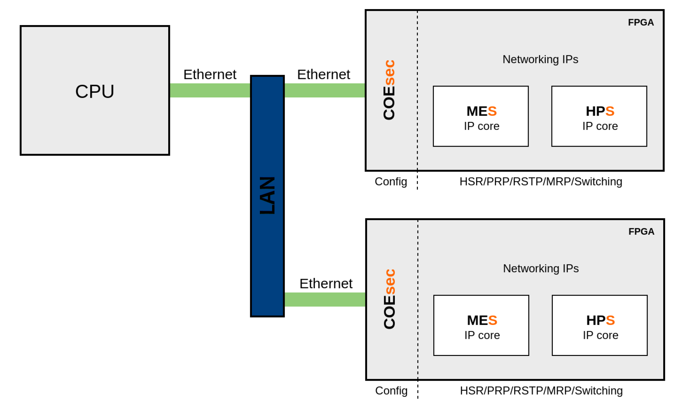
Figure 2 shows how networking IPs implemented in a FPGA can be securely configured by a CPU located in the same network. In this scenario, the CPU is responsible for both generating and receiving COEsec messages to configure the desired networking IPs. Furthermore, it behaves as a server that allows remote configuration in WAN using higher level protocols such as HTTPS.
In order to provide the required information to secure the communications, a custom frame format has been developed. COEsec messages are based on Ethernet frames that contain several specific fields within the Payload that provide all the cryptographic information and the configuration data. Figure 3 shows a COEsec frame including protocol specific fields and Ethernet fields.
As shown in Figure 3, COEsec data is divided in three main sections. The first one contains some data required for encryption/decryption tasks (Channel ID and IV). The second one includes the encrypted configuration data. Finally, a tag provides authentication and integrity to the messages. The fields that form the COEsec frame are:
- Channel ID: each COEsec communication is identified by a channel ID. This field is used to associate the sender/receiver to its secret key that is used to encrypt/decrypt and authenticate the messages. It is two bytes long. This field is stored in an FPGA register.
- Reserved: it is a four-bytes long field reserved for future use. All of them must be set to zero.
- IV: it is a twelve-bytes long initialization vector used for the encryption/decryption of the messages and it is needed to provide randomness to the messages and to ensure confidentiality. It is divided in two sub-fields: a random number and a frame number.
- -
- Random Number: it is an eight-bytes long random number that allows the encryption algorithm to achieve semantic security and prevents an attacker from inferring relationships between segments of different encrypted messages.
- -
- Frame Number: it is a four-bytes long frame number that identifies each couple of messages (i.e., petition and response) exchanged between a sender and a receiver and, it is associated to a certain channel ID. The sender should increase the frame number with each new frame. In case of the sender using an invalid frame number, an automatic response message will be generated, the response contains the same frame number that the petition received and whose payload will contain the valid frame number expected to receive for that channel ID. When the maximum frame number value is reached, the value should be reset to zero.
- Payload: it contains the encrypted configuration commands (both reading and writing operations) and their respective responses. There are two types of COE commands: read and write.To read a register, it is necessary to provide the address associated with the register to be read and an operation identifier. The command would be as follows:where “x” is the memory address to be read (16 bits) and R is the identifier of the command (R-Read).To write a register, it is necessary to provide the address associated with the register to be written, the data to be written to the register and an operation identifier. The command would be as follows:where “x” is the memory address to be written (16 bits), “d” is the data to write (32 bits) and W is the identifier of the command (W-Write).
- Authentication Tag: in order to prevent an attacker from modifying the messages, an authentication tag is used (16 bytes long). This tag has been generated using a Hash function which assures that if any of the bits of the authenticated fields changes, the tag will take a different value. The authenticated fields are: Channel ID, Reserved, IV and Payload, as well as, the Ethernet header (MAC destination, MAC source and Ethertype).
3. Implementation
In this section, the proposed secure protocol and IP core are evaluated according to the resource utilization and module latency.
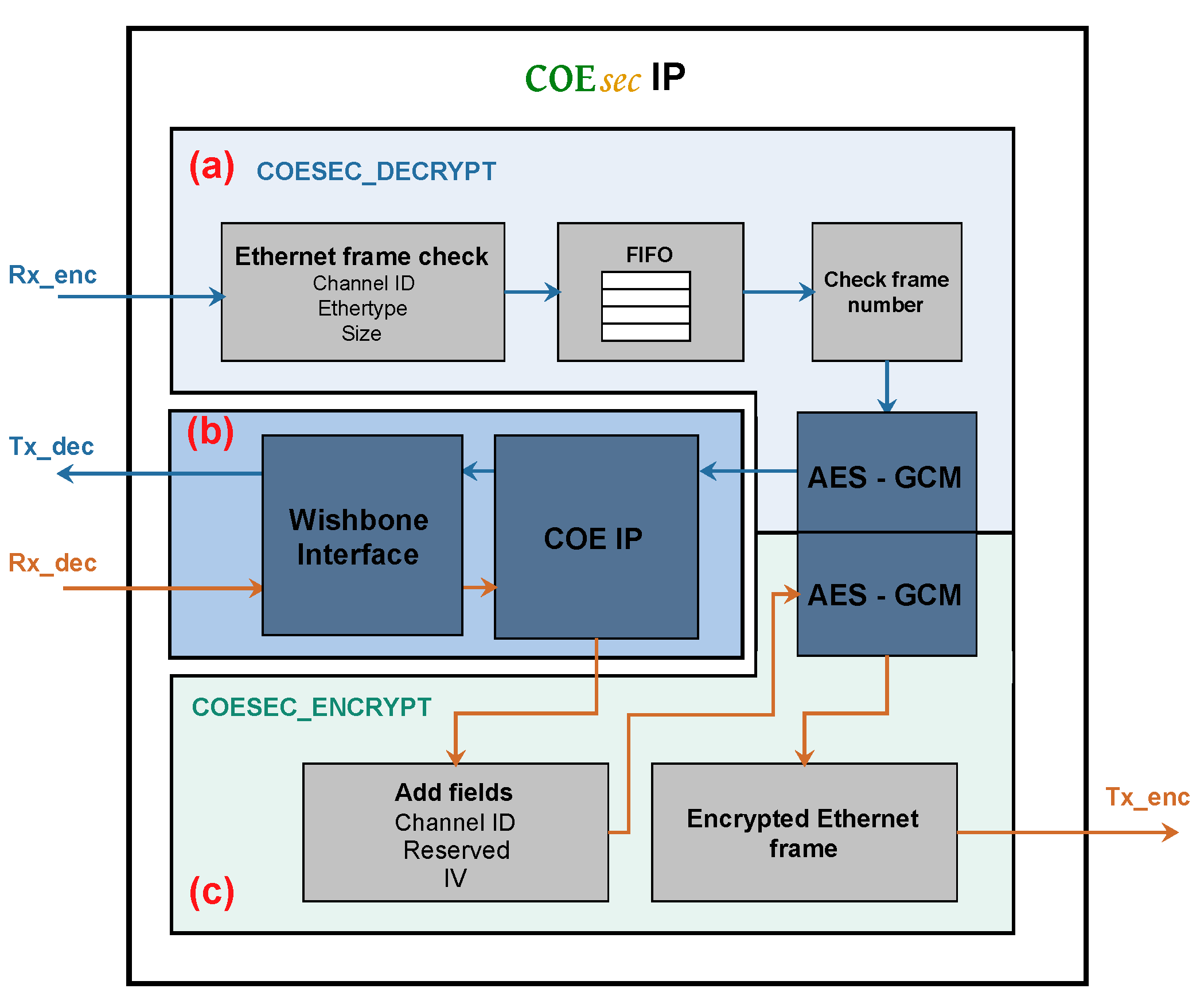
Figure 4 depicts the block diagram for implementing the proposed COEsec architecture. The operation principle is described as follows:
When a new Ethernet frame is received by the COEsec IP Core, at first, there is a check to deermine whether the frame contains a valid Ethertype, whether it belongs to a valid channel (Channel ID), and whether it has a frame size within the limits set in the IP configuration. If the validation is positive, the frame is stored in a FIFO memory with several frames capacity. Otherwise, the frame is discarded.
The frames that have been stored in the FIFO memory are processed one by one. First, there is a check to determine whether the frame number is valid for the channel associated with it or not. If the frame number is wrong, the frame is discarded and a response frame will be generated. This response frame has the same frame number, and the Payload contains the expected frame number for the channel and 14 bytes to zero. Conversely, if the frame number, the Ethertype, and Channel ID are valid, the frame is sent to an AES-GCM module, which is responsible for decrypting and authenticating the frame. In this regard, if the frame is correctly authenticated it is sent, without the Channel ID, Reserved, and IV fields) to the COE IP Core. Note that in this process the original Payload has been replaced by the COE decrypted command. Conversely, if the frame is not authenticated, the frame is discarded. The same operation is performed with the next frame in the FIFO memory.
Once a valid decrypted frame is sent to the COE, the COEsec waits to receive the COE response. When the response is received, the Channel ID, Reserved, and IV fields are added to the received frame by the COEsec IP Core and it sends the frame to the AES-GCM module to encrypt and generate the authentication tag. Finally, the encrypted frame is built and it is transmitted.
In order to describe the hardware of the proposed architecture, the VHDL code and the synthesis process for a reconfigured SoC XC7Z020 from Xilinx Zynq is used. This device is mounted on SoCe SmartZynq industrial networking board, which is used to validate the proposed architecture.
The amounts of resources, in percentage, needed for implementing the proposed COEsec, shown in Figure 4 are presented in Table 1. As can be seen, the implementation of the COE module without the security protocol requires 2.48% of the resources in the worst-case scenario. If we compare with the implementation of the encryption protocol (COEsec), an additional 6.44% of resources is necessary, in short, the proposed COEsec implementation requires 8.92% of the total resources available on the FPGA.
If we compare the COEsec module with the switching infrastructure implemented in the FPGA the overhead added to the design represents 37.41% of the entire used resources, as shown in Figure 5. Table 2 summarizes this comparison.
With the purpose of determining the COEsec latency introduced in the design, the architecture presented in Figure 5 is implemented.
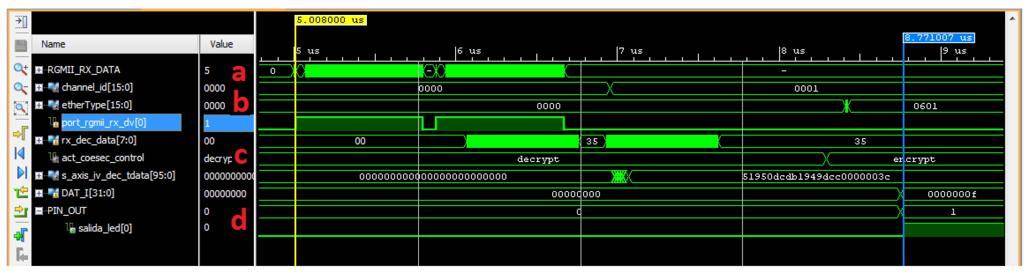
The architecture shown in Figure 5 comprises a 4-port IEEE1588-aware Managed Ethernet Switch (MES) IP [25], an IEEE1588 Timer and Timestamping IP, a COEsec IP instance, and a simple Wishbone [26] system interconnection architecture. The IP switching and timing infrastructure implemented in the FPGA can be configured by means of any Ethernet ports, since all COE frames are addressed to the COEsec IP that processes them and configures the IP through the Wishbone Master interface. The proposed design is simulated by means of Vivado Simulator to verify its proper performance. A screen capture of the simulation in the COEsec module is shown in Figure 6.
Moreover, the simulations are used to determine the processing time of a COEsec frame from it entering the core until the data is saved in the IP core register to be configured. In addition, simulations for writing and reading frames using different transmission rates (e.g., 10 Mbps, 100 Mbps, 1 Gbps) are performed, the results of which are summarized in Table 3.
4. Validation
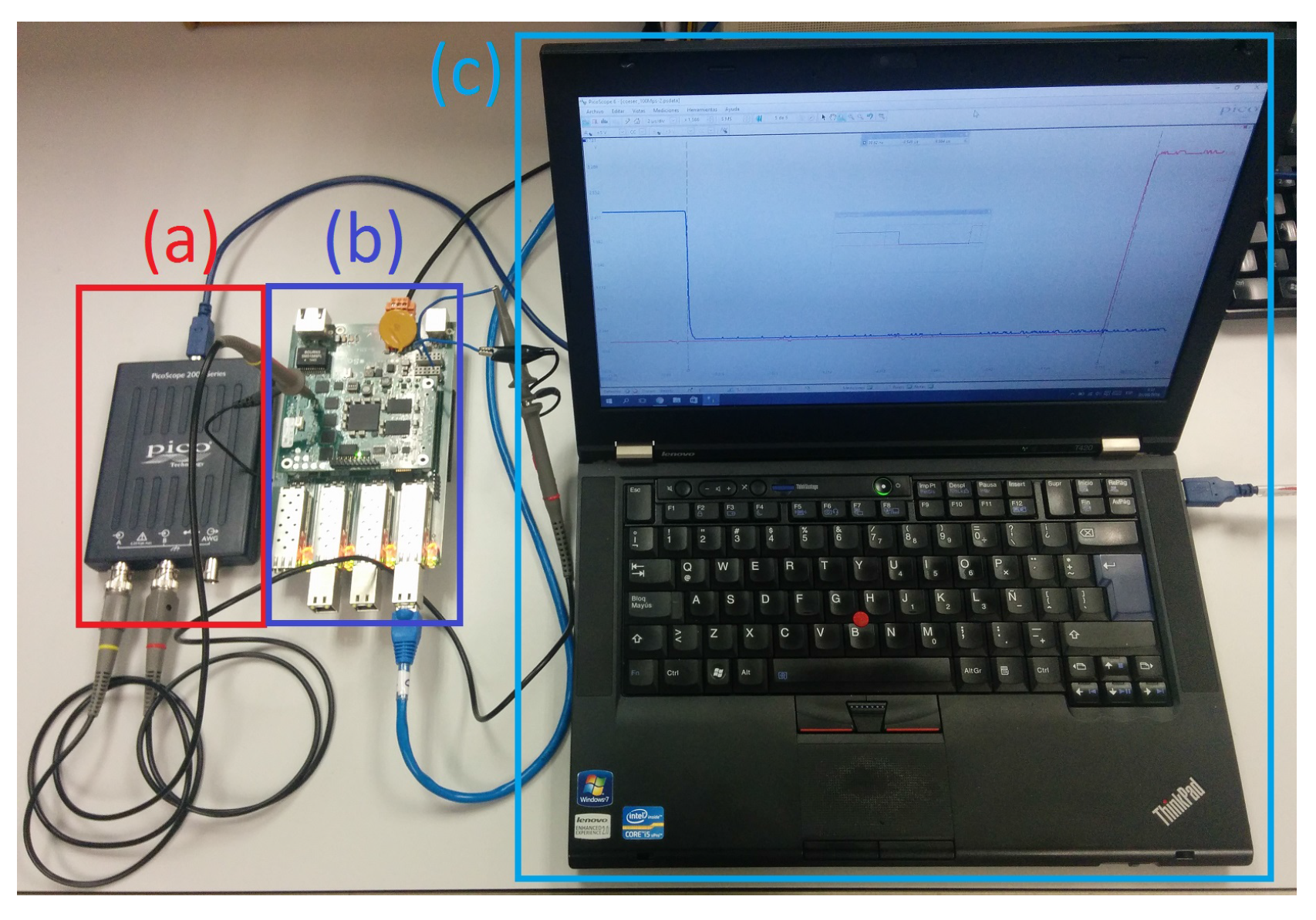
The proposed architecture described in the previous section is validated in a proof of concept using the configuration depicted in Figure 7. It is composed by a PC, an FPGA based card (SMARTzynq Industrial Networking card [27]) and a multiport oscilloscope. In this scenario, a PC is responsible for sending and receiving the COEsec frames, which are generated by means of Python scripts.
The COEsec module testing is performed as follows:
First, a ciphered writing frame to one internal register of the IP in the FPGA is sent from the PC. Next, a reading frame to the previous register is sent from the PC. This command triggers a response from the FPGA to the PC that is ciphered. The response (i.e., reply) frame is captured through WireShark software. Finally, the frame is decrypted using a Python script that includes a third party-implementation of the cipher suite, which delivers the register value that should match with the value sent in the writing frame.
In order to measure the ‘real’ processing time (including the Ethernet PHY chips and additional logic) an oscilloscope has been included in the set-up, Figure 7. The oscilloscope first channel gets the Ethernet frame before entering the PHY in the Rx+ pin. The second channel is connected to the FPGA pin linked to the state of the register, which is being configured. In addition, the second channel is used as a trigger signal. Figure 8 details the setup outlined in Figure 7.
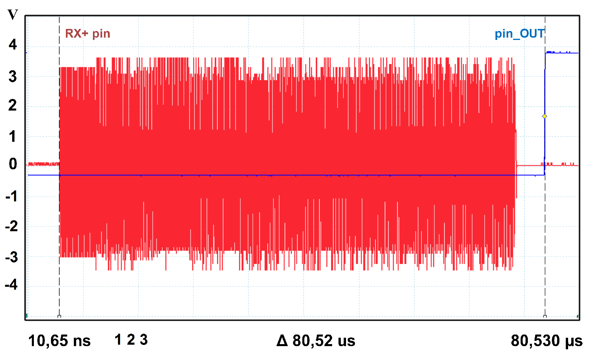
Figure 9 shows the capture for a 10 Mbps writing frame. As can be seen, the time that it takes from the frame enters to the PHY until a change on the output pin is s.
Moreover, the difference between the time obtained by simulation (i.e., s) and the time obtained by the oscilloscope are is result of the latency produced in the PHY from entering the first bit to the output of the first data through the Rdx(3:0) bus. In this case, the delay is s, which is approximated to s according to the value specified in the datasheet of the PHY shown in Table 4.
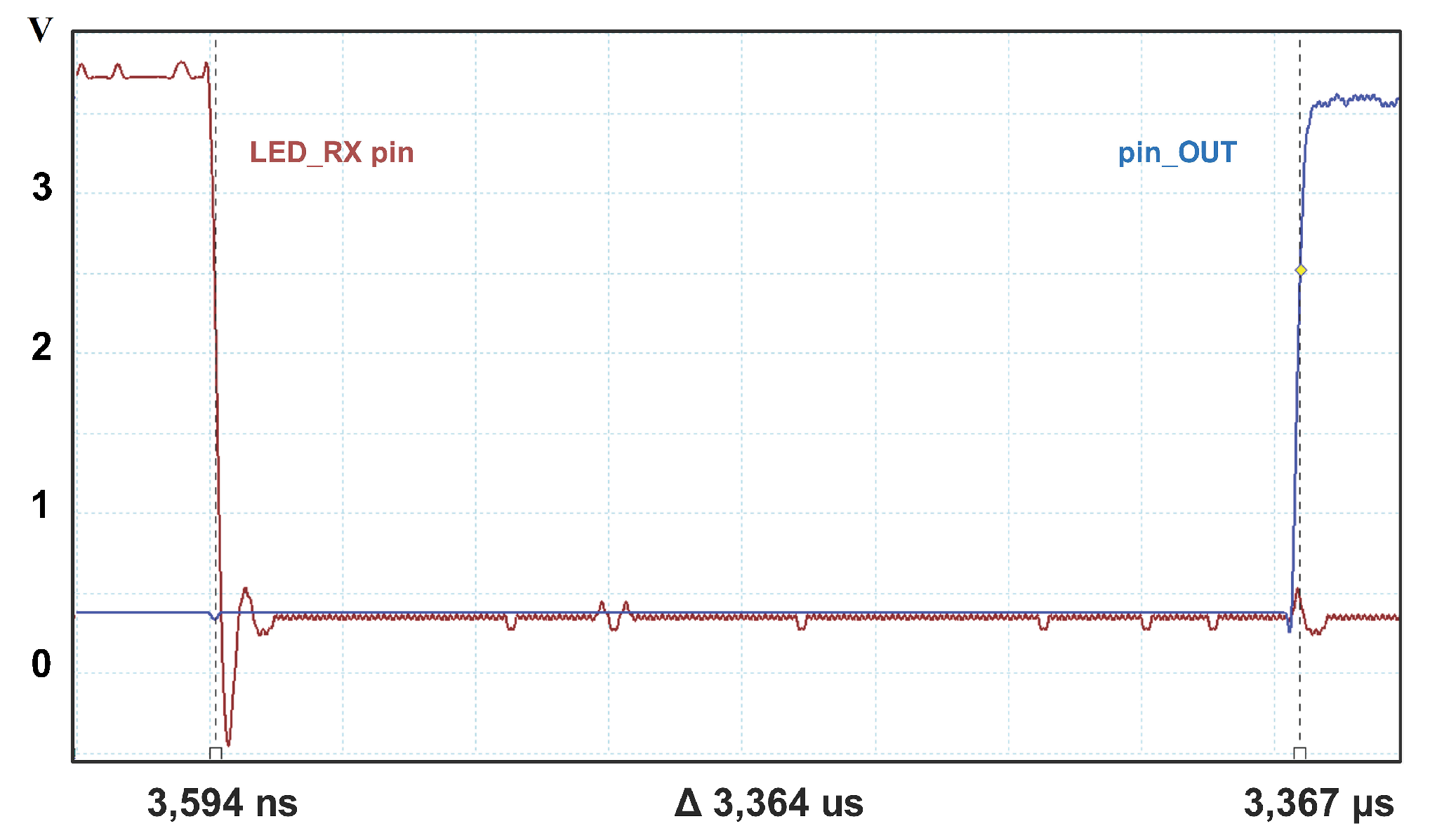
Furthermore, for measurements at rates of 100 Mbps and 1 Gbps, the first channel is connected to the LED RX pin of the PHY, which reports when a frame is received. Figure 10 shows the capture for a 1 Gbps rate obtaining a processing time of s, which is similar to the s obtained by simulation. Note that for obtaining the total processing time, it is necessary to consider the latency introduced by the PHY.
Finally, Table 5 presents the results obtained by simulation and in the real set-up. As can be seen, the experimental results follow the evolution obtained in simulations. In addition, the similarity of the data presented in Table 5 highlights the correct performance and reliability of the used measurement method.
5. Comparison with Existing Schemes
In Table 6, a comparison between the proposed work and previous studies that focus on the configuration of the FPGA through Ethernet links is presented. In [7,8,9,10] the FPGA designs including a processor to manage Ethernet frames, which greatly increases the overhead of FPGA resources are presented. In [7,9] use as encryption algorithm Output Feedback (OFB) and [8] uses Cipher Feedback (CBC). In [28], algorithms implemented in the FPGA to manage Ethernet frames are used, but no encryption method is used. In the proposed work the processing of the frames is performed using algorithms implemented in the FPGA, this approach allows reducing the resource usage and the processing time of the Ethernet frames. In addition, the proposed architecture utilizes the AES-GCM as an encryption algorithm. It is clear that our solution uses fewer resources, which was to be expected because in the implementation a microprocessor is not used to manage the Ethernet frames. In the papers analyzed, there is no information regarding the processing time to make a comparison. In our case, it was necessary to determine the processing time because the objective is to provide security in the field of the Smart Grid where processing times are critical.
6. Conclusions
A solution for a secure protocol and IP core for configuration of networking hardware IPs implemented in the FPGA using CPU located on the same network is proposed in this work. The FPGA based implementation presented, proposing a light Layer-2 protocol, fully implemented on hardware and protected by strong cryptographic algorithms (AES-GCM). The secure protocol and IP core are validated in hardware used in cutting-edge Smart-Grid installations. The implementation results highlight the small silicon footprint required to implement the solution, enabling it for cost-sensitive CPU-less solutions but applying the state-of-the-art cryptographic algorithms. In addition, the timing obtained for the on-the-fly decryption of the frames enables the extension of this approach to secure other critical control frames used in Smart-Grid environment. Future work in this topic will focus on the research to integrate this approach over TSN networks and to analyze other AES implementations that could offer similar results from the performance point-of-view, but with even more reduced resources usage. The processing times of the ethernet frames show that this encryption method can be applied to the guaranteed GOOSE and SV frames that are executed in the 3 ms recommended by the IEC 61850 standard.
Acknowledgments
This work has been supported by the Ministerio de Economía y Competitividad of Spain within the project TEC-2017-84011-R and it has been carried out inside the Research and Education Unit UFI11/16 of the UPV/EHU and partially supported by the Basque Government within the fund for research groups of the Basque university system IT978-16 and within the project TFactory ER-2014/0016. Also, FEDER funds, UPV/EHU, and Universidad de las Fuerzas Armadas ESPE through a PhD scholarship funding are acknowledged.
Author Contributions
The overall research has been performed by Marcelo Urbina and Mikel Rodriguez providing all the necessary knowledge and development in the area of hardware implementation. Naiara Moreira and Tatiana Acosta have been in charge of the development of state of the art. Jesús Lázaro and Armando Astarloa have provided feedback on multiple areas and has developed many of the Ethernet frame encryption.
Conflicts of Interest
The authors declare no conflict of interest.
References
- Jiang, X. High Availability Seamless Ring Protocol Implementation in FPGA. Master’s Thesis, Swiss Federal Institute of Technology (Zurich), Zurich, Switzerland, 2009. [Google Scholar]
- Araujo, J.A. Alta Fiabilidad Por Redundancia en Redes Industriales Sobre Ethernet. Master’s Thesis, Faculty od Engineering, University of the Basque Country, Vizcaya, Spain, 2011. [Google Scholar]
- A System Solution for IEDs Based on IEC 61850; Analog Devices: Norwood, MA, USA, 2013.
- Reyrolle 7SR110 & 7SR120 Argus. SIEMENS: Munich, Germany, 2017. Available online: http://w3.siemens.com/smartgrid/global/en/products-systems-solutions/Protection/overcurrent-feeder-protection/Pages/7SR110-7SR120.aspx (accessed on 22 January 2018).
- IEC 61850 Substation Control and Automation Devices; Arteche Group: Mungia, Spain, 2017.
- IEC 61850 on HSR/PRP Communication Modules from SoC-e; SystemCORP Embedded Technology: Beckenham, Australia, 2017.
- Kashyap, H.J. Secure Dynamic Reconfiguration of FPGAs. ACM Trans. Reconfig. Technol. Syst. 2014, 7. [Google Scholar] [CrossRef]
- Devic, F.; Torres, L.; Crenne, J.; Badrignans, B.; Benoît, P. SecURe DPR: Secure update preventing replay attacks for dynamic partial reconfiguration. In Proceedings of the International Conference on Field Programmable Logic and Applications, (FPL ), Oslo, Norway, 29–31 August 2012; pp. 57–62. [Google Scholar]
- Vliegen, J.; Mentcns, N.; Verbauwhede, I. A single-chip solution for the secure remote configuration of FPGAs using bitstream compression. In Proceedings of the International Conference on Reconfigurable Computing and FPGAs, (ReConFig), Cancun, Mexico, 9–11 December 2013. [Google Scholar]
- Castillo, J.; Huerta, P.; Martínez, J.I. Secure IP downloading for SRAM FPGAs. Microprocess. Microsyst. 2007, 31, 77–86. [Google Scholar] [CrossRef]
- Kevin, P. Slammer Worm Crashed Ohio Nuke Plant Network. SecurityFocus, Register 2003, 20, 1–4. Available online: http://www.securityfocus.com/news/6767 (accessed on 23 January 2018).
- Kushner, D. The Real Story of Stuxnet. IEEE Spectr. 2013, 50, 48–53. [Google Scholar] [CrossRef]
- Fairley, P. Cybersecurity at U.S. Utilities Due For an Upgrade. IEEE Spectr. 2016, 53, 11–13. [Google Scholar]
- North American Electric Reliability Council. SQL Slammer Worm Lessons Learned for Consideration by the Electricity Sector; Technical Report; NERC: Atlanta, Georgia, 2003. [Google Scholar]
- Liu, J.; Xiao, Y.; Member, S.; Li, S.; Liang, W.; Chen, C.L.P. Cyber Security and Privacy Issues in Smart Grids. IEEE Commun. Surv. Tutor. 2012, 14, 981–997. [Google Scholar] [CrossRef]
- Ericsson, G. Cyber Security and Power System Communication—Essential Parts of a Smart Grid Infrastructure. IEEE Trans. Power Deliv. 2010, 25, 1501–1507. [Google Scholar] [CrossRef]
- Cleveland, F. IEC TC57 WG15: IEC 62351 Security Standards for the Power System Information Infrastructure; White Paper ver 14; International Electrotechnical Commission: Geneva, Switzerland, 2012. [Google Scholar]
- International Electrotechnical Commission. IEC-TS 62351-6 ed1.0 Power Systems Management and Associated Information Exchange—Data and Communication Security—Part 6. Security for IEC 61850; IEC: Geneva, Switzerland, 2007. [Google Scholar]
- International Electrotechnical Commission. IEC 61850-1 ed2.0 Communication Networks and Systems for Power Utility Automation—Part 1. Introduction and Overview; IEC: Geneva, Switzerland, 2013. [Google Scholar]
- Fuloria, S.; Anderson, R.; McGrath, K.; Hansen, K.; Alvarez, F. The Protection of Substation Communications. In Proceedings of the SCADA Security Scientific Symposium, Miami, FL, USA, 17–18 January 2010. [Google Scholar]
- Fries, S.; Falk, R. Security Considerations for Multicast Communication in Power Systems. Int. J. Adv. Secur. 2013, 6, 111–121. [Google Scholar]
- Dworkin, M. Recommendation for Block Cipher Modes of Operation Methods and Techniques, 2001. Available online: https://nvlpubs.nist.gov/nistpubs/SpecialPublications/NIST.SP.800-38G.pdf (accessed on 22 January 2018).
- Montes, M.; Penazzi, D. Dos nuevos algoritmos de cifrado autenticado. Silver y CPFB. Workshop Segur. Inform. 2014, 2014, 31–45. [Google Scholar]
- Usselmann, R. Advanced Encryption Standard/Rijndael IP Core. 2002. Available online: https://opencores.org/project,aescore,downloads (accessed on 22 January 2018).
- SoC-e. MES, Managed Ethernet Switch IP Core. 2016. Available online: http://soc-e.com/mes-managed-ethernet-switch-ip-core/ (accessed on 22 January 2018).
- WISHBONE System-on-Chip (SoC) Interconnection Architecturefor Portable IP Cores. Technical Report, 2002. OPENCORES.ORG. Available online: https://cdn.opencores.org/downloads/wbspec_b3.pdf (accessed on 22 January 2018).
- SoC-e. SMARTzynq Module: 5 Port Gigabit Ethernet Industrial Embedded Switch Module. 2016. Available online: http://soc-e.com/products/smart-zynq-module/ (accessed on 22 January 2018).
- Mishra, V.; Chen, Q.; Zervas, G. REoN: A Protocol for Reliable Software-Defined FPGA Partial Reconfiguration over Network. In Proceedings of the International Conference on Reconfigurable Computing and FPGAs, (ReConFig), Cancun, Mexico, 30 November–2 December 2016. [Google Scholar]
Figure 1.
New generation System-on-Chip (SoC) based intelligent electronic devices (IEDs). Include the IEEE 1588 support, HSR/PRP and Crypto-core IP.
Figure 1.
New generation System-on-Chip (SoC) based intelligent electronic devices (IEDs). Include the IEEE 1588 support, HSR/PRP and Crypto-core IP.
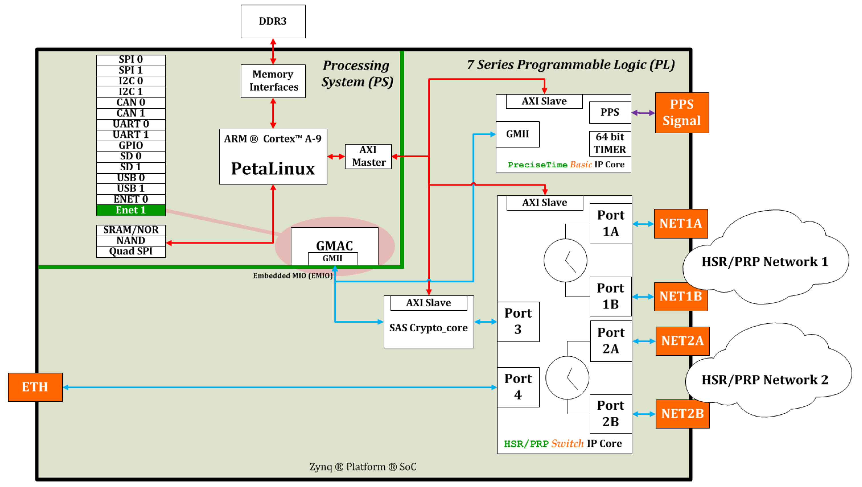
Figure 2.
CPU-FPGA communication. Networking CPU-less Intellectual Properties (IPs) implemented in both FPGAs can be securely configured by a CPU located in the same network.
Figure 2.
CPU-FPGA communication. Networking CPU-less Intellectual Properties (IPs) implemented in both FPGAs can be securely configured by a CPU located in the same network.

Figure 3.
Configuration Over Ethernet secure (COEsec) frame format. (a) Data required for encryption/decryption tasks (Channel ID and IV). (b) Encrypted configuration data. (c) Tag that provides authentication and integrity to the messages.
Figure 3.
Configuration Over Ethernet secure (COEsec) frame format. (a) Data required for encryption/decryption tasks (Channel ID and IV). (b) Encrypted configuration data. (c) Tag that provides authentication and integrity to the messages.
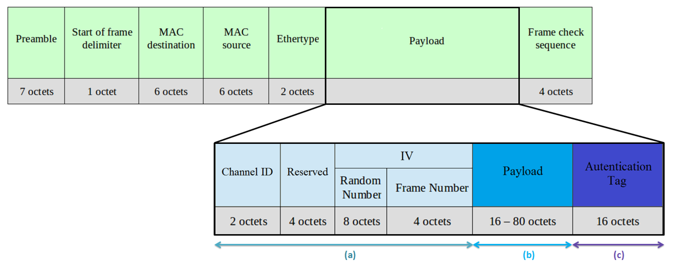
Figure 4.
Block diagram of the COEsec architecture implementation. (a) Module for reception, validation, and decryption of COEsec frames. (b) Module to establish communication between the COEsec and the IP core, all through bus Wishbone. (c) Module to generate, encrypt and transmit COEsec frames.
Figure 4.
Block diagram of the COEsec architecture implementation. (a) Module for reception, validation, and decryption of COEsec frames. (b) Module to establish communication between the COEsec and the IP core, all through bus Wishbone. (c) Module to generate, encrypt and transmit COEsec frames.

Figure 5.
Architecture to measure COEsec timing. Includes (a) 4-port Managed Ethernet Switch (MES) IP. (b) IEEE1588 Timer and Timestamping IP. (c) COEsec IP instance.
Figure 5.
Architecture to measure COEsec timing. Includes (a) 4-port Managed Ethernet Switch (MES) IP. (b) IEEE1588 Timer and Timestamping IP. (c) COEsec IP instance.
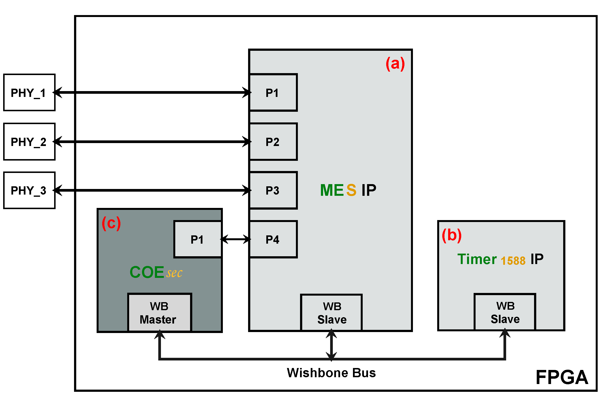
Figure 6.
COEsec module simulation for writing frame. (a) The frame is captured (i.e., writing process) initially. (b) Verify whether the Ethertype and Channel ID fields are valid. (c) The frames stored in the FIFO memory are sent to the AES-GCM module, for decrypting and authenticating the frame. (d) Finally, the data are sent to the COE IP, which decodes and executes the command COE.

Figure 7.
Concept-proof set-up for module COEsec. The oscilloscope is used to measure the time required to process a COEsec frame since it enters the Ethernet interface until the internal register is modified.
Figure 7.
Concept-proof set-up for module COEsec. The oscilloscope is used to measure the time required to process a COEsec frame since it enters the Ethernet interface until the internal register is modified.
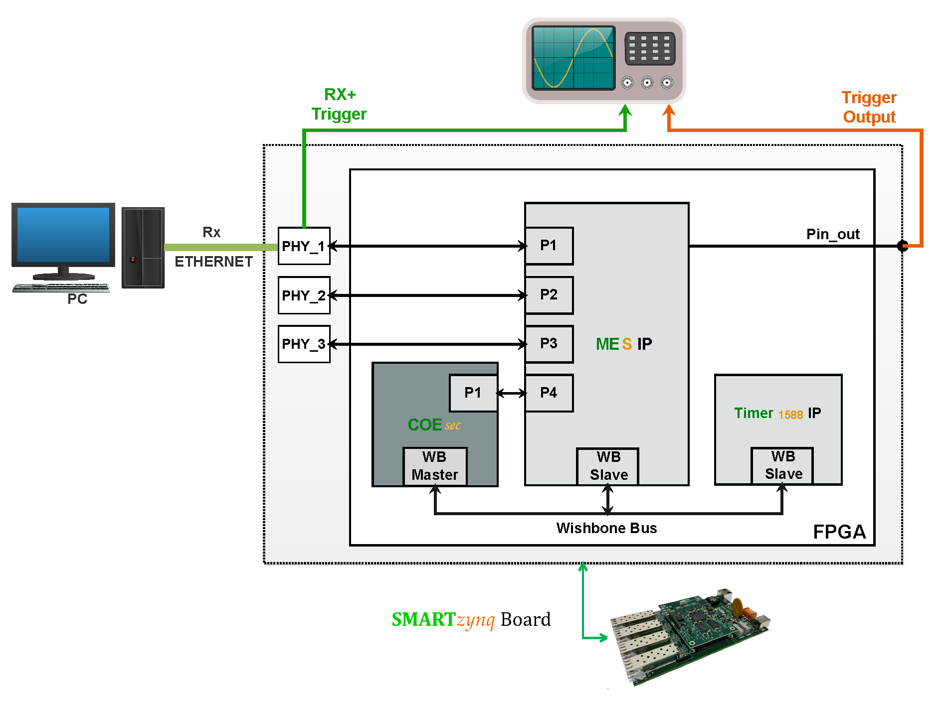
Figure 8.
Snap-shoot of SmartZynq COEsec concept-proof set-up. (a) Multiport oscilloscope. (b) SMARTzynq Industrial Networking card. (c) PC for sending and receiving the COEsec frames.
Figure 8.
Snap-shoot of SmartZynq COEsec concept-proof set-up. (a) Multiport oscilloscope. (b) SMARTzynq Industrial Networking card. (c) PC for sending and receiving the COEsec frames.

Figure 9.
Writing frame capture at 10 Mbps. Frame reception to cryptographic processing end can be seen. Total time from beginning of frame to output is s.
Figure 9.
Writing frame capture at 10 Mbps. Frame reception to cryptographic processing end can be seen. Total time from beginning of frame to output is s.

Figure 10.
Writing frame capture at 1 Gbps. Frame reception to cryptographic processing end can be seen. Total time from beginning of frame to output is s.
Figure 10.
Writing frame capture at 1 Gbps. Frame reception to cryptographic processing end can be seen. Total time from beginning of frame to output is s.

Table 1.
Field Programmable Gate Array (FPGA) resources used for the COEsec module implementation.
| Resources | COE without Security | COEsec with Security | Available | Percent COE without Security | Percent COEsec with Security |
|---|---|---|---|---|---|
| Slice Registers | 1215 | 4138 | 106,400 | 1.14 % | 3.89 |
| Slice LUT | 1318 | 4748 | 53,200 | 2.48 % | 8.92 |
| Block RAMs | 0.5 | 5.5 | 140 | 0.36 % | 3.93 |
Table 2.
COEsec comparison with switching infrastructure implemented on the FPGA.
| Resources | COEsec | Switching Infrastructure IPs | Full Design | Percent COEsec | Percent Switching Infrastructure IPs |
|---|---|---|---|---|---|
| Slice Registers | 4138 | 9522 | 13,660 | 30.29 % | 69.71 |
| Slice LUT | 4748 | 7942 | 12,690 | 37.41 % | 62.59 |
| Block RAMs | 5.5 | 31 | 36.5 | 15.06 % | 84.94 |
Table 3.
COEsec processing times.
| Type | 10 Mbps | 100 Mbps | 1 Gbps |
|---|---|---|---|
| Reading | s | s | s |
| Writing | s | s | s |
Table 4.
PHY receive latency timing.
| Link | Parameter | Typ | Units |
|---|---|---|---|
| 1000 BASE-T | Star of Packet to RX_CTL Asserted | 236 | ns |
| 100 BASE-T | Star of Packet to RX_CTL Asserted | 357 | ns |
| 10 BASE-T | Star of Packet to RX_CTL Asserted | 2.18 | s |
Table 5.
Simulation data vs. measurement.
| Rates | Frame Writing | ||
|---|---|---|---|
| Simulation + PHY-Latency (s) | Measurement (s) | Percent Deviation (%) | |
| 10 Mbps | 80.376 | 80.520 | 0.18 |
| 100 Mbps | 10.509 | 10.650 | 1.34 |
| 1 Gbps | 3.600 | 3.364 | 0.47 |
Table 6.
Comparison with related works that focus on the configuration of a FPGA through Ethernet links, regarding their type of implementation (method to manage Ethernet frames), security properties (Encryption and Authentication), and the amounts of resources that are used in an FPGA (overhead).
Table 6.
Comparison with related works that focus on the configuration of a FPGA through Ethernet links, regarding their type of implementation (method to manage Ethernet frames), security properties (Encryption and Authentication), and the amounts of resources that are used in an FPGA (overhead).
| Feature | [7] | [8] | [9] | [10] | [28] | This Work |
|---|---|---|---|---|---|---|
| Microprocessor | Yes | Yes | Yes | Yes | no | no |
| Encryption | AES (OFB) | AES (CBC) | AES (OFB) | DES | no | AES (GCM) |
| Authentication | HMAC (256) | HMAC (256) | HMAC (256) | MD5 | no | GMAC |
| Communication | Ethernet | Ethernet | Ethernet | local | Ethernet | Ethernet |
| Resources | ||||||
| Slice Registers | 13,600 | 10,124 | 9740 | - | 1083 | 4138 |
| Slice LUT | 13,305 | 13,470 | - | 7102 | 13,862 | 4748 |
| Block RAMs | 65 | 35 | 69 | - | 117 | 5.5 |
| DSP | 10 | 3 | 7 | - | - | - |
| Overhead (FPGA) | high | high | high | low | high | low |
© 2018 by the authors. Licensee MDPI, Basel, Switzerland. This article is an open access article distributed under the terms and conditions of the Creative Commons Attribution (CC BY) license (http://creativecommons.org/licenses/by/4.0/).
Share and Cite
MDPI and ACS Style
Urbina, M.; Moreira, N.; Rodriguez, M.; Acosta, T.; Lázaro, J.; Astarloa, A. Secure Protocol and IP Core for Configuration of Networking Hardware IPs in the Smart Grid. Energies 2018, 11, 510. https://doi.org/10.3390/en11030510
AMA Style
Urbina M, Moreira N, Rodriguez M, Acosta T, Lázaro J, Astarloa A. Secure Protocol and IP Core for Configuration of Networking Hardware IPs in the Smart Grid. Energies. 2018; 11(3):510. https://doi.org/10.3390/en11030510
Chicago/Turabian StyleUrbina, Marcelo, Naiara Moreira, Mikel Rodriguez, Tatiana Acosta, Jesús Lázaro, and Armando Astarloa. 2018. "Secure Protocol and IP Core for Configuration of Networking Hardware IPs in the Smart Grid" Energies 11, no. 3: 510. https://doi.org/10.3390/en11030510
Note that from the first issue of 2016, this journal uses article numbers instead of page numbers. See further details here.