Single-Phase Shunt Active Power Filter Based on a 5-Level Converter Topology
by
 ,
,
José Gabriel Oliveira Pinto
1,* ,
,
Rui Macedo
2,
Vitor Monteiro
1, 
Luis Barros
1,
Tiago Sousa
1 and
João L. Afonso
1 1
Centro ALGORITMI—University of Minho, Campus de Azurém, 4800-058 Guimarães, Portugal
2
Department of Industrial Electronics, University of Minho, Campus de Azurém, 4800-058 Guimarães, Portugal
*
Author to whom correspondence should be addressed.
Energies 2018, 11(4), 1019; https://doi.org/10.3390/en11041019
Submission received: 14 March 2018
/
Revised: 12 April 2018
/
Accepted: 16 April 2018
/
Published: 22 April 2018
(This article belongs to the Special Issue Power Electronics and Power Quality)
Abstract
:This paper presents a single-phase Shunt Active Power Filter (SAPF) with a multilevel converter based on an asymmetric full-bridge topology capable of producing five distinct voltage levels. The calculation of the SAPF compensation current is based on the Generalized Theory of Instantaneous Reactive Power (p-q theory) modified to work in single-phase installations, complemented by a Phase-Locked Loop algorithm and by a dedicated algorithm to regulate the voltages in the DC-link capacitors. The control of the SAPF uses a closed loop predictive current control, followed by a multilevel Sinusoidal Pulse-Width Modulation technique with two vertical distributed carriers, which were specially conceived to deal with the asymmetric nature of the converter legs. Along the paper, some simulation results are used to show the main characteristics of the 5-level converter and control algorithms, and the hardware topology and control algorithms are described in detail. In order to demonstrate the feasibility and performance of the proposed SAPF based on a 5-level converter, a laboratory prototype was developed and experimental results obtained under diverse conditions of operation, with linear and non-linear loads, are presented and discussed in this paper.
1. Introduction
The field of power electronics has experienced a major development in the last decades, allowing for the utilization of electrical loads with higher efficiency for a vast range of appliances. Nonetheless, this development is still present nowadays and it shows a predisposition to continue in the future [1,2]. An overview of the key considerations for an improved utilization of both presently used and upcoming power devices is presented in [3]. Despite its provided benefits, the development of power electronics shifted the paradigm of electrical loads from linear to non-linear, i.e., the current in this type of load presents a waveform different from the supplied voltage, which is due to a production of harmonic currents [4]. Harmonic currents are harmful to the power systems since they contribute to overheating, for instance, in power transmission cables and transformers, and interfere with communication systems. As such, power transmission cables and transformers should be derated due to harmonic currents flowing, which carries additional costs [5,6]. Harmonic currents can be produced by loads such as adjustable speed drives [7], arc furnaces [8], cycloconverters [9], electric vehicle battery chargers [10], lighting equipment, such as compact fluorescent and LED lamps [11], among other domestic appliances. Therefore, power quality, and especially harmonic currents, has deserved significant attention throughout the years.
The compensation of harmonic currents was primarily performed by passive filters. However, these are bulky and are only capable of compensating a limited range of harmonics. Besides, passive filters can produce resonance phenomena when connected to the power grid [12]. On the other hand, Shunt Active Power Filters (SAPFs) are power electronics devices that are capable of compensating harmonic currents, power factor and current imbalances in three-phase systems. Moreover, the compensation capability of a SAPF is dynamic, i.e., it is capable of compensating the aforementioned power quality problems regardless of the loads connected to the power grid. The operation of a SAPF consists in producing the harmonic currents and reactive power required by the connected loads, so that, the power grid currents acquire a sinusoidal waveform in phase with the voltages. Although this operation principle was proposed in [13], the SAPF was initially presented in [14] and, since then, has gained popularity due to the referred advantages over the traditional compensation systems [15]. Furthermore, several control theories for SAPFs have been developed and described in the literature, with the p-q theory [16], the FBD [17], the CPC [18] and the synchronous reference frame d-q theory [19] being among the main methods for obtaining the compensation currents for SAPFs. An extended review concerning control algorithms for SAPFs is presented in [20].
Regarding its structure, a SAPF is a DC-AC power converter, which can be either of the voltage source type or the current source type [21]. Moreover, a DC-AC power converter can be also classified in accordance with the number of levels of the output voltage or current, whereby it is considered a multilevel converter if the number of levels is three or more [22]. Multilevel converters are advantageous for medium voltage applications since they are capable of providing higher output voltages than the voltage that power semiconductors have to withstand. Besides, multilevel converters produce less dv/dt and have a better performance in terms of Total Harmonic Distortion (THD) when compared to two-level converters [23]. There are three classical topologies of multilevel converters, namely the neutral point clamped (or diode clamped) [24], the flying capacitor (or capacitor clamped) [25], and the cascaded multilevel converter [26]. Nevertheless, several topologies have been proposed in the literature, aiming to achieve higher numbers of levels with reduced switch counts [27,28,29,30,31]. Accordingly, control and modulation techniques for multilevel converters have been also widely investigated [32,33].
In this context, this paper presents a single-phase SAPF composed of a 5-level converter topology. The principle of operation of the proposed converter is explained in detail, from the implemented power theory to the applied modulation technique. Simulation results are depicted to analyze the feasibility of the converter. A laboratory prototype was developed and tested in real conditions of operation. The obtained experimental results validate the implemented single-phase 5-level SAPF hardware topology and control algorithms. The main contributions of this paper are: a low digital resource for the control theory implementation, which is based on the concepts introduced by the p-q theory, adapted to work in single-phase installations, and combined with a Phase-Locked Loop (PLL) to allow sinusoidal currents at the source side; a Sinusoidal Pulse-Width Modulation (SPWM) modulation strategy based on the vertical distribution of two triangular carriers that deals with the asymmetries of the 5-level converter legs; a comprehensive description of the hardware prototype development and a step-by-step validation of the control algorithms.
2. Proposed 5-Level Converter Topology
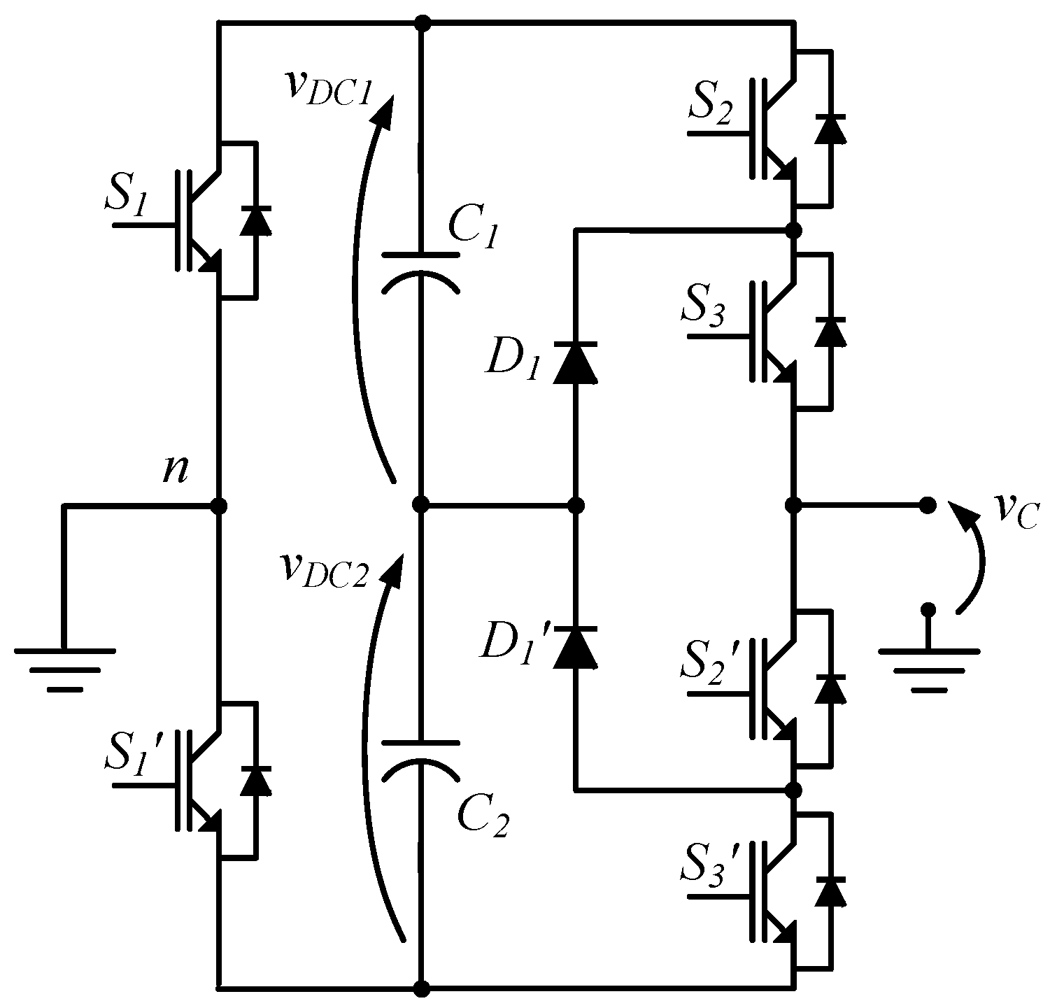
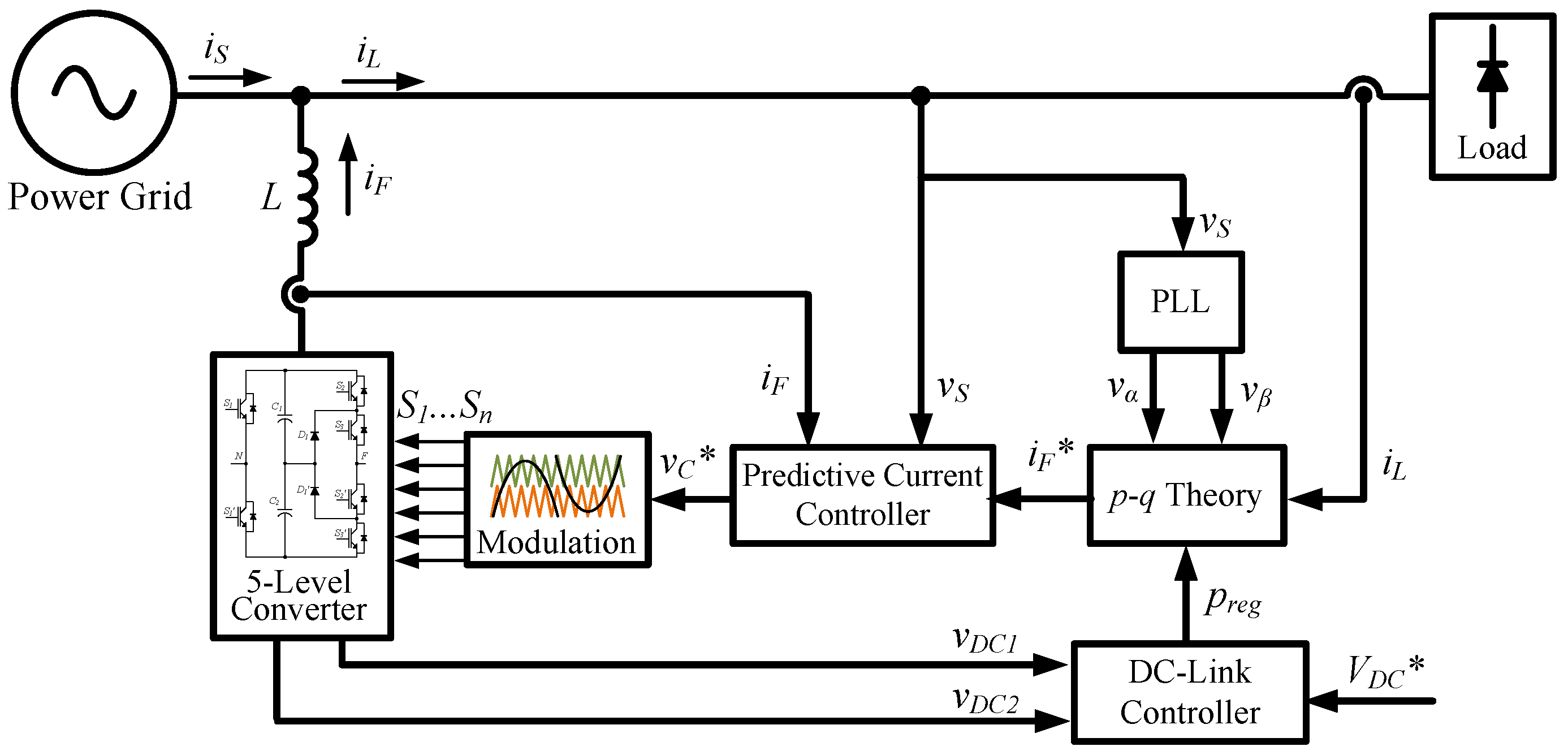
This section introduces a detailed description of the 5-level converter topology, which is depicted in Figure 1. As it can be seen, it is constituted by a three-level Diode-Clamped Multilevel Inverter (DCMLI) leg and by a two-level leg. The DC-link is composed of two capacitors in order to obtain the different voltage levels during both positive and negative half-cycles.
A relevant characteristic of the 5-level converter is the asymmetrical switching frequency of each leg, as well as the nominal voltage that each semiconductor of both legs withstands. The two-level leg (formed by S1 and S1’) is responsible for the polarity of the AC voltage and the switching frequency of this leg is equal to the fundamental frequency of the voltage to be synthetized by the converter, i.e., equal to the frequency of the power grid voltage, in this work. The semiconductors of this two-level leg should be able to support a voltage of vDC, i.e., the sum of the voltage across each capacitor of the DC-link (vDC1 and vDC2). On the other hand, the DCMLI leg (formed by S2, S2’, S3, and S3’) is controlled in order to establish the voltage level that the converter should produce (vDC, vDC/2 or 0) in both positive and negative half-cycles. This leg is switched with a higher frequency in comparison with the switching frequency of the two-level leg and is responsible for defining the converter state in each half-cycle, and, therefore, for defining the waveform of the produced voltage. By increasing the switching frequency, it is possible to improve the quality of the produced voltage, resulting in an improved compensation current. The semiconductors of the DCMLI leg should be able to support a nominal voltage of vDC/2, i.e., the voltage of each DC-link capacitor, which is half of the voltage that the semiconductors of the two-level leg should support.
The different states that the 5-level converter can assume during the positive and negative half-cycles are presented in Table 1. This table illustrates that the semiconductors S1 and S1’ are switched at the fundamental frequency of the produced voltage, and the other semiconductors (S2, S2’, S3, and S3’) are switched to establish the different voltage levels.
3. Control Algorithms
This section introduces the proposed control algorithms for the SAPF based on a 5-level converter, including a description about the p-q theory complemented by a Phase-Locked Loop (PLL) and adapted to work with single-phase installations, the DC-link control, the predictive current control, and the SPWM strategy.
3.1. p-q Theory
The p-q theory was initially developed to be applied in the analyses of three-phase three-wire electrical systems and later, it was expanded to three-phase four-wire systems to be usable in unbalanced systems with zero sequence components [34,35]. With some modifications, it is also possible to use the p-q theory in the analyses of single-phase systems [36]. The basics of this time-domain theory resides in a transformation of referential from the a-b-c coordinates, where the fundamental voltages are shifted by 120° for each other, to the α-β-0 orthogonal system of coordinates. The change in the coordinates referential is performed by the application of the Clarke transformation to the voltages,
and to the currents,
of the installation under analysis. After the transformations, it is possible to calculate the instantaneous real power (p), the instantaneous imaginary power (q), and the instantaneous zero sequence power (p0), applying:
Each one of the instantaneous powers calculated by Equation (3) can be decomposed in an average value and an oscillating value:
where the average value of the instantaneous real power (), is related to the energy that is transferred in a continuous way from the source to the loads and is associated with the active power. The oscillating value of the instantaneous real power (), is related to a parcel of energy that is exchanged between the source and the load. The average and oscillating values of the instantaneous real power ( and ) relates to the energy that is transferred and exchanged with the help of the neutral conductor. The instantaneous imaginary power components ( and ) are associated with the presence of storage elements (capacitors or inductors) in the loads, and are related to energy that is exchanged between the source and loads or between the loads with the help of the source. In three-phase systems, the average value of the instantaneous imaginary power () is exchanged between the three-phases of the system and is not associated with any effective energy transfer from the source of the loads. However, the presence of this component results in an increase in the source currents. The adoption of the p-q theory to calculate the compensation currents for a SAPF results from the physical interpretation of the power components described above. The power components that are involved with an effective energy transfer from the source to the load are the average value of the instantaneous real power () and the average value of the instantaneous zero sequence power (). Therefore, in an installation with a SAPF, these components are the only power components that should be supplied by the source, while all the other components should be provided by the SAPF. However, is transferred with the help of the neutral conductor, and so, it contributes to an increase in the current in the neutral conductor, which is an undesired phenomenon. Nevertheless, with a three-phase four-wire SAPF and with an appropriate control algorithm, it is possible to transfer the energy related to the average value of the zero-sequence power, in an equilibrated way by the three phases of the system, and so, eliminating the current in the neutral conductor upstream of SAPF. The calculation of the compensation currents that the SAPF must produce to eliminate the undesired power components, which are supplied by the source, can be accomplished by:
where , and are the references for the compensation currents of the SAPF in the α-β-0 coordinates. In order to obtain the references for the compensation currents in the a-b-c coordinates, it is used the inverse Clarke transformation, defined as:
According to this procedure, it is possible to apply the p-q theory to separate the desired power components from the undesired ones, and, therefore, develop a control algorithm for a SAPF to eliminate the undesired power components and improve the power quality of the installation. With a balanced and sinusoidal three-phase system, the application of the compensation strategy, based on p-q theory, results in balanced and sinusoidal currents in the source. However, if the voltages are distorted and unbalanced, by the application of the p-q theory, the source currents become neither sinusoidal nor balanced, which is a disadvantage. To overcome this drawback, it is possible to use the positive sequence of the fundamental components of the source voltages instead of the real ones, and so, the compensation results always in sinusoidal and balanced currents in the source, even with distorted and unbalanced voltages. The positive sequence of the fundamental components of the voltages can be obtained by the application of a PLL algorithm. There are interesting PLL algorithms in the literature, for three-phase systems [34] and for single-phase [35].
The application of the p-q theory to single-phase systems requires the emulation of a balanced three-phase system. For that, the voltages and currents in phases b and c are obtained applying a phase shift of ±120° to the measured voltage and current in phase a. The application of the Clarke transformation to a three-phase balanced system produces two equal α and β components shifted by 90° degrees, one from the other. Therefore, it is possible to implement the emulation of a three-phase, balanced system, directly in the α-β-0 coordinates, by applying:
and
where T is the period of the power grid fundamental frequency, and corresponds to a time delay of , which corresponds to a phase shift of +90° in the fundamental frequency. It is important to explain that, in a balanced three-phase system, the zero sequence power component does not exist and, therefore, the reference for the compensation current for a single-phase SAPF can be calculated by [36]:
Also, in single-phase systems it is possible to use PLL algorithms combined with the p-q theory to obtain sinusoidal currents at the source side. In this work, it was used the PLL algorithm described in [35].
3.2. DC-Link Voltage Control
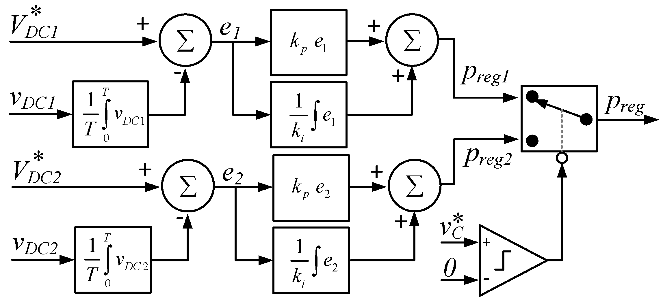
In order to the SAPF produce the compensation current, it is necessary to guarantee that the total DC-link capacitors voltage is greater than the peak value of the source voltage. The regulation of the DC-link capacitors voltage, in steady state, is done by absorbing a small amount of active power from the power grid, which corresponds to the converter losses. During some transients, it can be necessary to absorb or to deliver active power to the power grid, in values which can be greater than the ones involved in steady state. This is required to maintain the capacitors voltage regulated. In this way, it is necessary to include an additional instantaneous real power parcel (preg) in the calculation of the references for the SAPF compensation currents. The value of preg is determined by means of a PI controller that eliminates the error between the DC-link voltages and the reference value. It is important to explain that, during the normal operation of the SAPF, the oscillating values of the power components defined by the p-q theory are exchanged between the loads and the DC-link capacitors of the SAPF, and so, it is natural that the DC-link capacitors voltage oscillates to compensate these power components. Taking into account this situation, the objective of the DC-link voltage control algorithm is to regulate the average values of the DC-link capacitor voltages (VDC1 and VDC2) instead of the instantaneous values (vDC1 and vDC2). Therefore, the calculation of the errors is not performed by the difference between the reference voltage and the DC-link voltages, but by the difference between the reference and the average values of the DC-link capacitors voltage. Despite the possibility to use other values, in this work it was used an average value of an entire grid period.
As the DC-link of the SAPF is composed by two capacitors, it is necessary to take into account which capacitor is used in each instant, in order to select the correct value of preg and add it to the average value of the instantaneous real power () in Equation (12). The identification of the capacitor that is used in each time instant can be done by consulting Table 1, from where it is possible to conclude that capacitor C1 is used when the converter output voltage is negative and the capacitor C2 is used when the output voltage is positive. The block diagram of the DC-link voltage control is represented in Figure 2, and, as it is possible to see, two similar PI controllers are used to obtain the value of preg.
3.3. Predictive Current Control
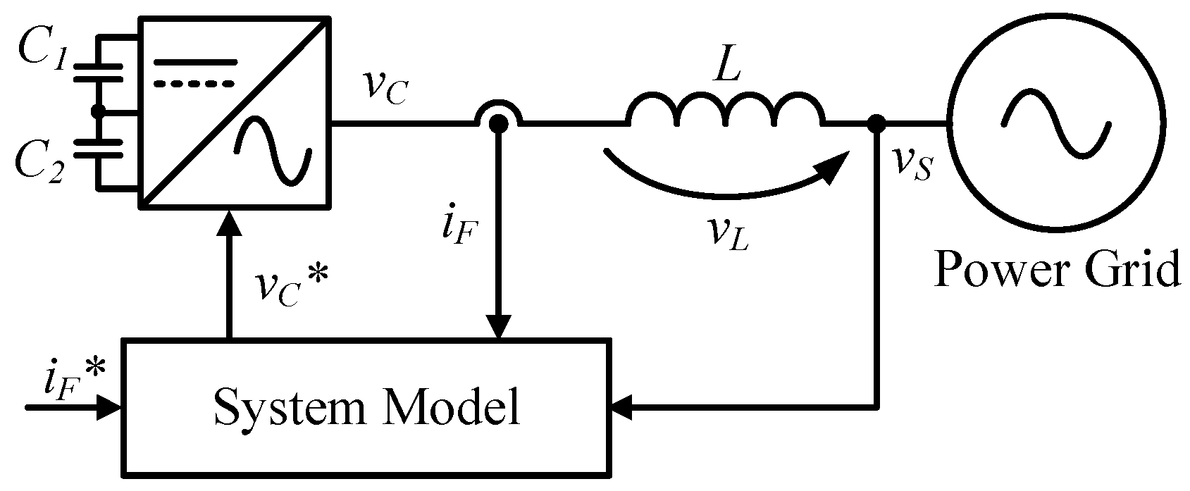
A predictive strategy was adopted to control the current in the AC side of the 5-level converter. This strategy requires measuring the values of the AC current (iF) and the source voltage (vS), which are obtained using a signal acquisition board, as well as the nominal values of the main electrical parameters of the system. Therefore, by analyzing the voltages and currents between the 5-level converter and the power grid, a set of equations can be established and used to predict the next state (i.e., during the time interval of [k, k + 1]) that the converter should assume in terms of produced voltage. By using this strategy, it is predictable that the filter current will follow its reference during each sampling time interval. The block diagram of the implemented predictive current control is illustrated in Figure 3.
The electrical model of this type of system, generally can be described by the source voltage (vS), by the converter output voltage (vC), and by the coupling passive filters voltage (vL), where, in this specific case, an inductor is used as a passive filter. Therefore, by analyzing the voltages in the AC side of the system, it is possible to establish the output voltage of the 5-level converter as a function of the source voltage and the voltage across the inductor, as described by:
Substituting the inductance voltage (vL) by the time derivative of its current multiplied by its nominal value, it is possible to obtain the equation:
where is also considered the voltage across the internal resistance of the inductor. Taking into account that the voltage in the resistive part is residual due to the reduced value of the internal resistance, it can be neglected, resulting in the equation:
As occurs in all the systems with a feedback control, also in this current control strategy an error between the reference signal and the measured current is calculated as:
Taking into account the electrical model of the system, it is possible to substitute the produced current (iF) established in Equation (14), allowing obtaining the equation:
Considering a digital implementation and using a high sampling frequency, the variation of the error derivative is almost linear and equal to the increase in the current error (ΔiFerror). Therefore, by selecting a high switching frequency, the resultant current ripple will be reduced and the error will be practically zero, i.e., the produced current will be centered in its reference. The current error can be obtained according to:
Taking into account the position of the sensors and implemented control algorithm, it is important to note that the voltage established by the converter should produce a current in phase opposition with the one established in Equation (18). In this way, changing the signal to the term ierror, it is obtained the control equation defined by:
Rearranging the terms in both sides of Equation (19), the final control equation is established according to:
Considering this final control equation, the output voltage is the reference of the voltage (vc*) used in the SPWM, i.e., the signal that is compared with the carrier. Taking into account that is used a digital platform to implement the control algorithm, the final control equation in discrete-time is obtained according to:
Using Equation (21), expanding the terms, a simplified equation is obtained according to:
Taking into account that this is a linear control, it has some characteristics that are similar to a traditional PI controller, however without the necessity to adjust the gains of the controller, which represents a relevant characteristic of the predictive current control strategy. However, the performance of the predictive current controller is strongly affected by the accuracy of the mathematical model of the circuit. In real implementations, the inductance value of the coupling inductor varies as a function of the frequency, current amplitude, and core temperature, adversely affecting the results.
3.4. SPWM Strategy
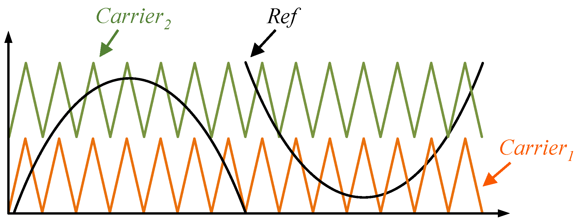
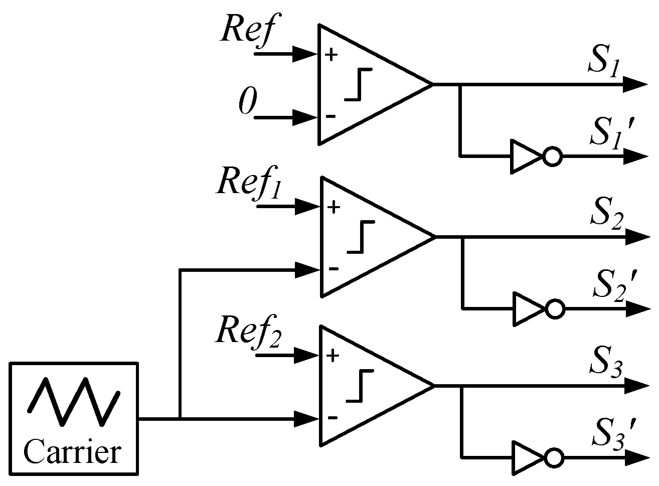
In order to produce the desired current, a modulation strategy is required to drive the IGBTs accordingly. Multilevel inverters require different SPWM arrangements than those required by two-level inverters, hence more than one triangular carrier is needed. The different carriers can be distributed either vertically or horizontally. Since the studied converter derives from the DCMLI topology, the adopted SPWM strategy is based on Phase Disposition (PD) modulation, i.e., the triangular carriers are vertically distributed and in phase with each other. However, an adaptation was performed in order to reduce the number of required triangular carriers. Hence, instead of using four carriers and a single reference signal, a single carrier and adapted reference signals are used.
Figure 4 shows the adopted strategy and Figure 5 shows the obtained reference signals to generate the IGBT gate commands. As it can be seen in Figure 4, the reference signal is used in two comparisons, one being used for emulating the upper carrier (Carrier2) and the other for the lower carrier (Carrier1). The comparisons between Ref and the two carriers can be accomplished by using a single carrier and two modified reference signals, which are obtained by means of a branch function. The reference signal in the positive Carrier1 level, i.e., when Ref is positive and inside the carrier amplitude, corresponds to the original reference. However, in the negative Carrier1 level, i.e., when Ref is negative and below the carrier amplitude, the reference signal consists in the sum of the original reference with twice the carrier amplitude. This reference signal corresponds to Ref1 in Figure 5. On the other hand, the reference signal in Carrier2 level in the positive half-cycle, i.e., when Ref is positive and above the carrier amplitude, is obtained by subtracting the original reference and the carrier amplitude. Finally, the reference signal in Carrier2 level in the negative half-cycle, i.e., when Ref is negative and inside the carrier amplitude, is attained by summing the original reference and the carrier amplitude. This signal corresponds to Ref2 in Figure 5. As it can be seen in Figure 5, a comparison with zero is performed, which corresponds to the polarity of the original reference. With this approach, a single triangular carrier can be used to achieve a 5-level PD modulation, which would require four carriers in the conventional implementation. Besides this advantage, the IGBTs S1 and S1’ switch at the line frequency (50 Hz), whereby switching losses are reduced.
Figure 6 presents a block diagram that shows an overview of the algorithms used to control the SAPF. As it is visible in the figure, the source voltage (vS) is used by the PLL algorithm to synchronize the SAPF controller with the fundamental component of the source voltage. Based in the α-β voltages calculated by the PLL algorithm, the DC-link regulation power (preg) and the load current (iL), the p-q theory calculates the compensation current (iF*). The compensation current is processed by the predictive current controller to obtain the reference voltage (vC*) of the converter. Finally, the modulation block defines the semiconductors that must be activated in each instant.
4. Simulation Analysis
This section presents a simulation analysis of the proposed single-phase 5-level SAPF, where the key control functionalities are described, such as the modulation strategy and DC-link voltage control, and both the transient and steady-state operation of the SAPF are analyzed. The simulations were performed using the software PSIM v9.1 from PowerSim, Inc (Rockville, MD, USA).
4.1. SPWM Strategy
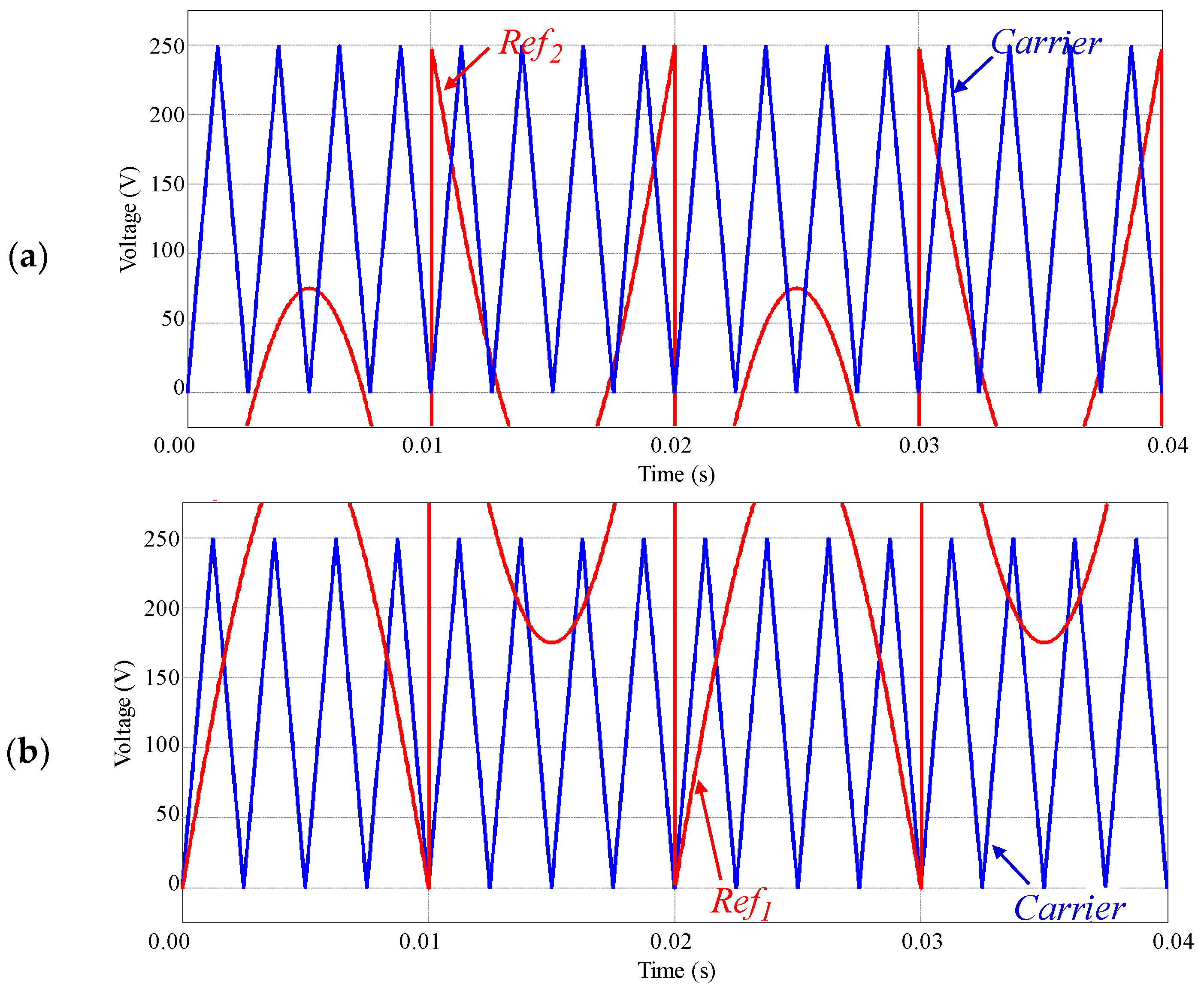
Figure 7 shows a simulation result of the implemented modulation strategy, where a sinusoidal signal was used as reference signal. As it can be seen, the reference signal is used in two comparisons, one for emulating the upper carrier (Ref2) and the other for the lower carrier (Ref1).
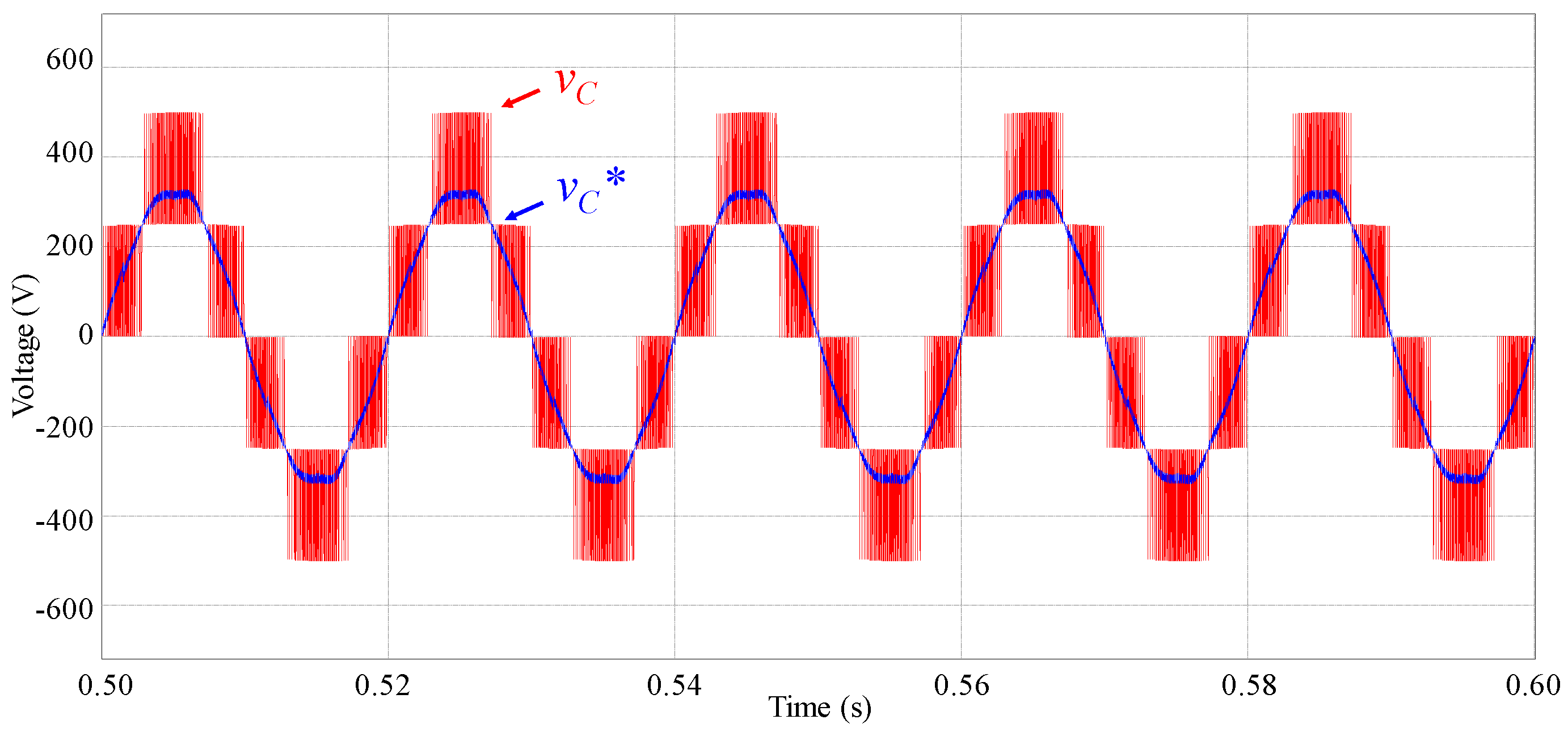
In order to assess the generation of the desired voltage levels based on the adapted SPWM strategy, Figure 8 depicts the output voltage produced by the 5-level converter (vc) and its reference (vc*). As it can be perceived, the converter is capable of producing the distinct 5 voltage levels according to the reference voltage established by the predictive current controller.
4.2. DC-Link Voltage Control
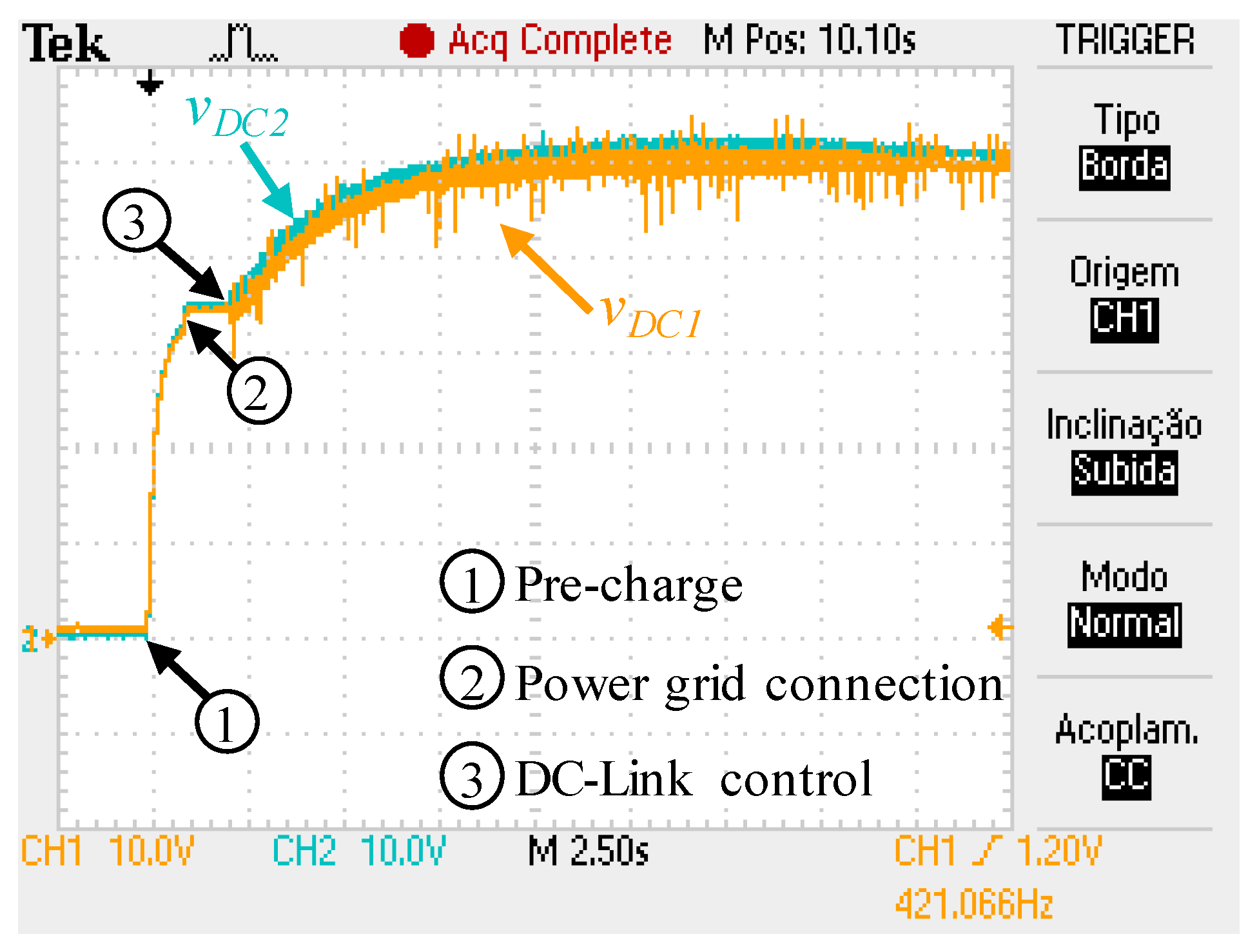
In order to assure a proper operation for the SAPF, the DC-link voltage must be controlled to an established reference voltage and its average value needs to be as constant as possible. However, since the SAPF is comprised by a voltage source converter and the DC-link capacitors are initially discharger, it cannot be directly connected to the power grid, during the start-up procedure, otherwise, the current absorbed by the DC-link capacitors via the IGBTs antiparallel diodes would damage the power converter. For this purpose, a pre-charge resistor is used, being bypassed when the DC-link voltage reaches a value close to the power grid peak voltage. After the bypass, the DC-link voltage control is activated, whereby the IGBTs are controlled so that the DC-link voltage reaches the established reference value. After this instant, the SAPF compensation is activated.
Figure 9 shows the referred stages of the DC-link voltage control. The first stage is visible between the instants 0 s and 1.1 s, where the pre-charge resistor connected in series with the AC side of the SAPF limits the current, and therefore, the rise of the DC-link voltage. After the instant 1.1 s, the resistor is bypassed, and the DC-link voltage control is activated. For this initial stage, the p-q theory uses only the preg power component, whereby the operation as SAPF is not performed during this period. Finally, the third stage starts only after the voltage in each DC-link capacitor reaches the established value of 250 V, which occurs at instant 2.7 s. From this instant, the p-q theory is used to calculate the compensation current, including all the power components, whereby the SAPF operation is activated. A slight decrease in the DC-link voltages (vDC1 and vDC2) can be noted when the compensation is activated, being shortly after restored by the DC-link control. Besides, a ripple component can be visible in both voltages, which is a result of the power exchange between the SAPF and the power grid. This power exchange is intrinsic to the operation of the SAPF and causes an oscillation with twice the power grid frequency. Therefore, instead of using the instantaneous value of the DC-link voltage in the PI controller, a full-cycle average value is used, so that the DC-link voltage oscillation can be admissible without making the control unstable.
4.3. SAPF Operation
This section presents several simulation results of the proposed SAPF for operation with different types of electrical loads, namely linear and non-linear loads. Both transient and steady-state conditions are analyzed.
4.3.1. SAPF Operating with Resistive-Inductive (RL) Load
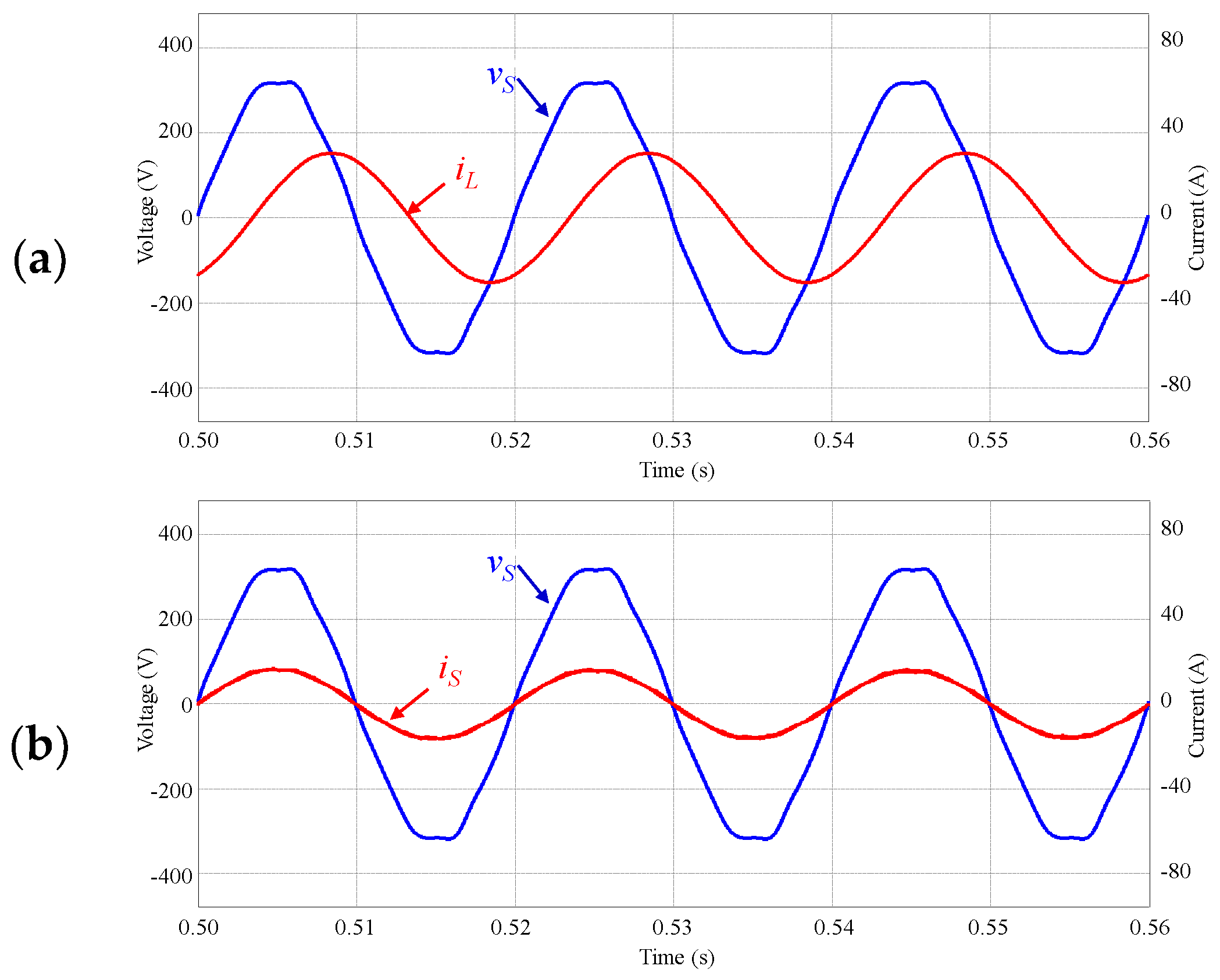
With the advances in power electronics, the number of linear loads has been reducing. However, there is still a considerable number of linear loads, such as, for example, the single-phase AC motors, which are good examples of RL loads. RL loads do not produce harmonic currents if supplied by a sinusoidal voltage, however, they produce reactive power. Since a SAPF is capable of compensating both harmonic currents and reactive power, the SAPF operation with linear loads should be considered. Therefore, a 30 mH inductor connected in series with a 7.5 Ω resistor was realized. Figure 10 depicts the source voltage (vS), which is equal to the load voltage, the current drawn by the load (iL), and the resulting source current in steady-state due to the SAPF operation (iS). As it can be seen, the displacement power factor is compensated to the unity by the SAPF operation. It is noticeable that the Root Mean Square (RMS) value of the source current decreases due to the improvement in the power factor (PF).
The transient caused by the SAPF starting of compensation, at t = 0.5 s, can be depicted in Figure 11. It is noticeable that the source current acquires a sinusoidal waveform in phase with the voltage almost instantly as the SAPF starts to compensate (t = 0.5 s), showing a good transient response of the SAPF.
4.3.2. SAPF Operating with Diode Rectifier with Resistive-Capacitive (RC) Load
The full-bridge diode rectifier with capacitive output filter and resistive load is one of the most common electrical loads used nowadays, and it is characterized by high level of harmonic current and low Power Factor (PF) due to the presence of harmonics. Real loads that use a diode rectifier with capacitive output filter are very common today as for example: computers, printers, CFL and LED lamps, TV-sets, cellphone chargers, etc. In order to assess the performance of the SAPF towards non-linear loads, the referred load was implemented in the simulation model, being used a 1 mF capacitor and a 16 Ω resistor connected in parallel to the rectifier output, and a 10 mH inductor connected in series with the rectifier input. Figure 12 depicts the load and source voltage (vS), the current drawn by the load (iL), and the resulting source current in steady-state due to the SAPF operation (iS). As it can be seen, the SAPF operation turns the source current sinusoidal and in phase with the source voltage, regardless of the harmonic distortion of the voltage.
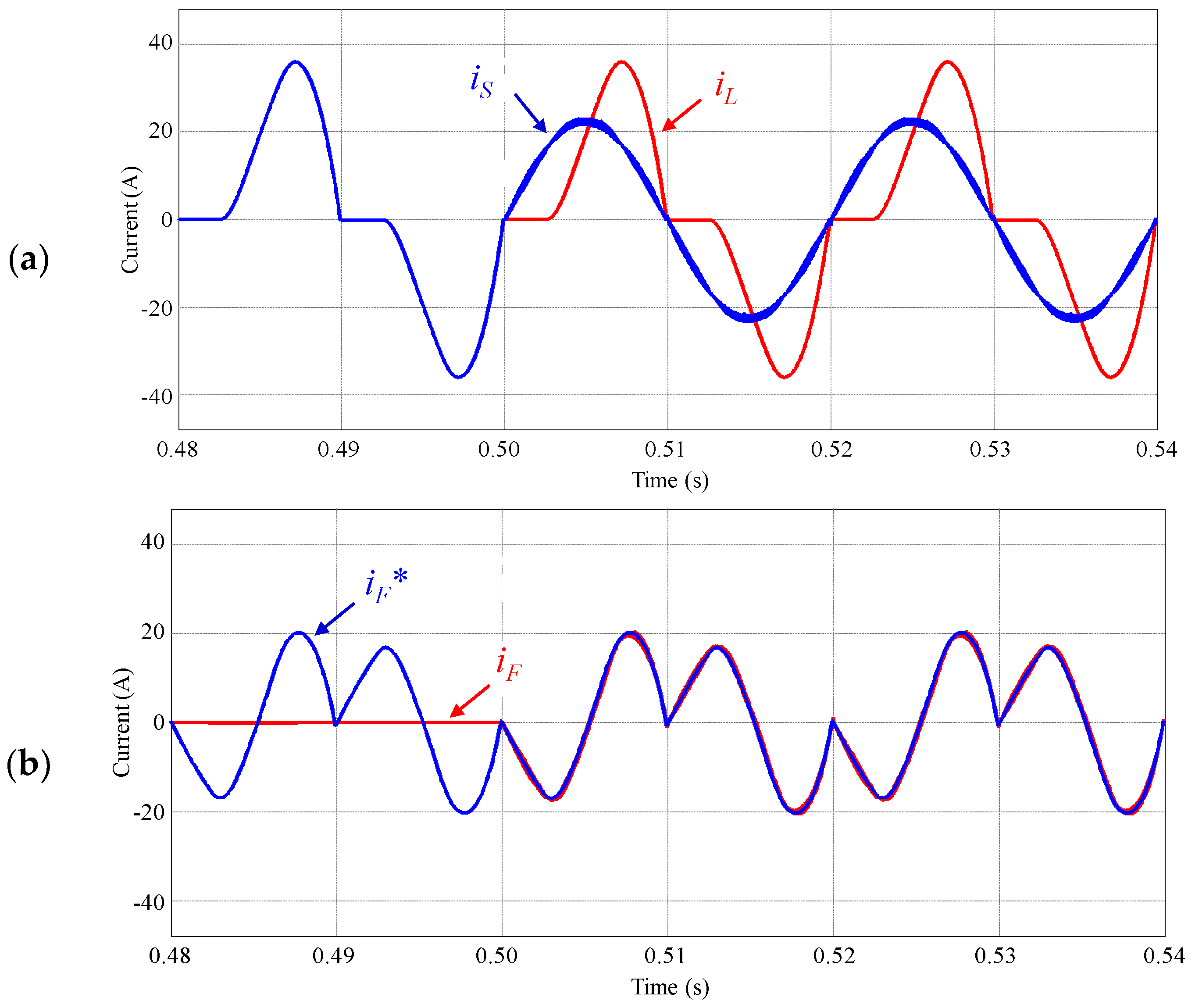
Figure 13 shows the transient state of the SAPF operation for the same load, where it can be seen the load current (iL), the source current (iS), the SAPF reference current (iF*) and the SAPF actual compensation current (iF). Once again, it is noticeable that the source current acquires a sinusoidal waveform in phase with the source voltage immediately when the SAPF operation begins, showing a good transient response of the SAPF operating with non-linear loads.
4.3.3. SAPF Dynamic Response towards Load Changing
In order to perform a more insightful analysis of the transient response of the SAPF, its operation towards changes in the connected loads was simulated. Therefore, two non-linear loads were connected to the power grid namely a diode rectifier with output RC load, initially connected, and a diode rectifier with output RL load.
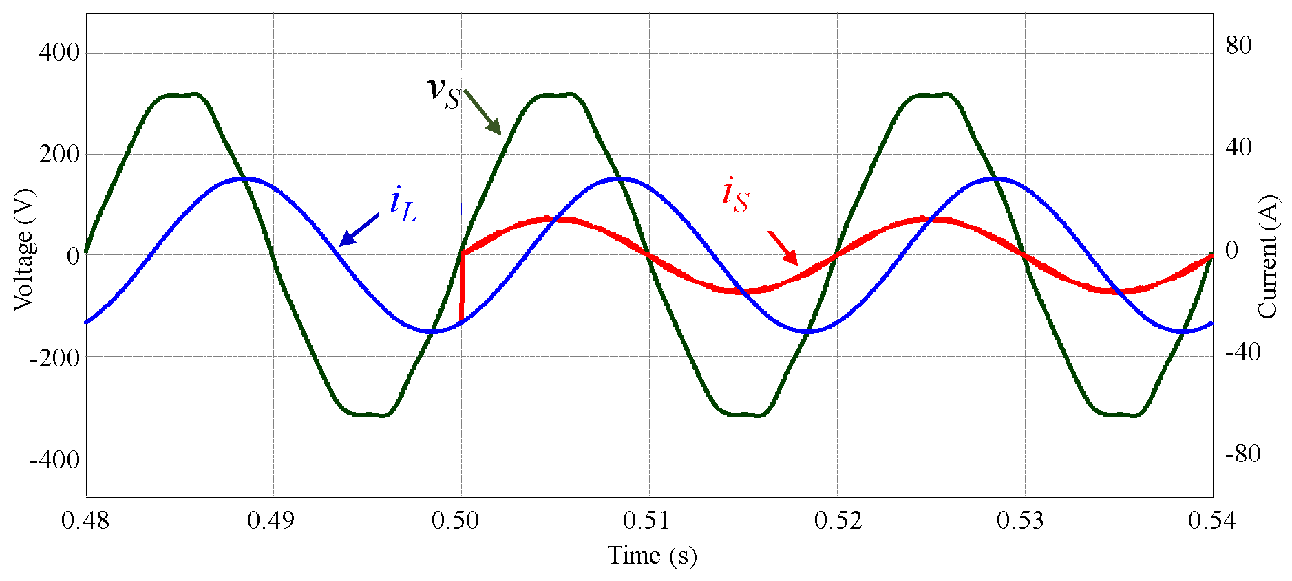
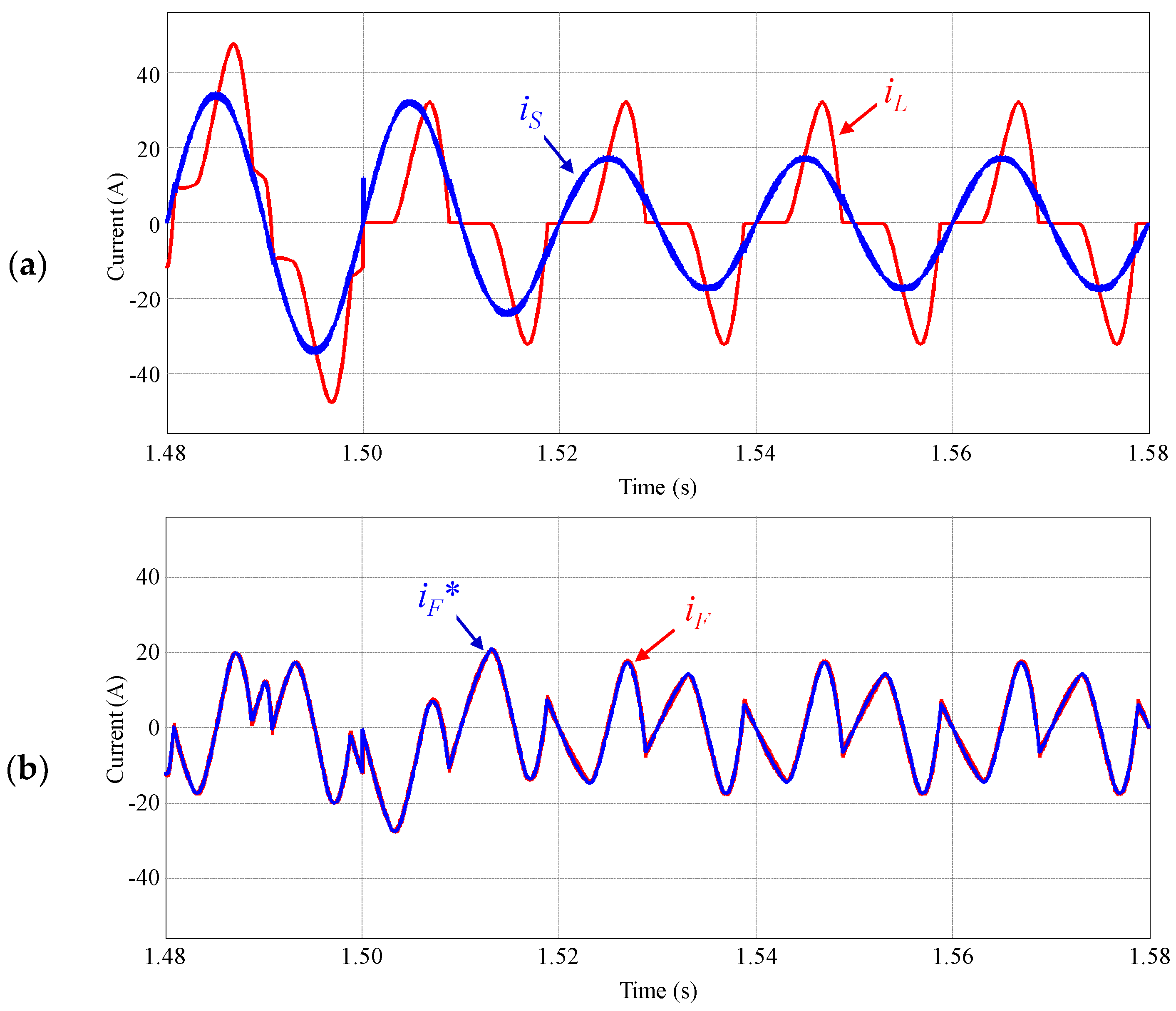
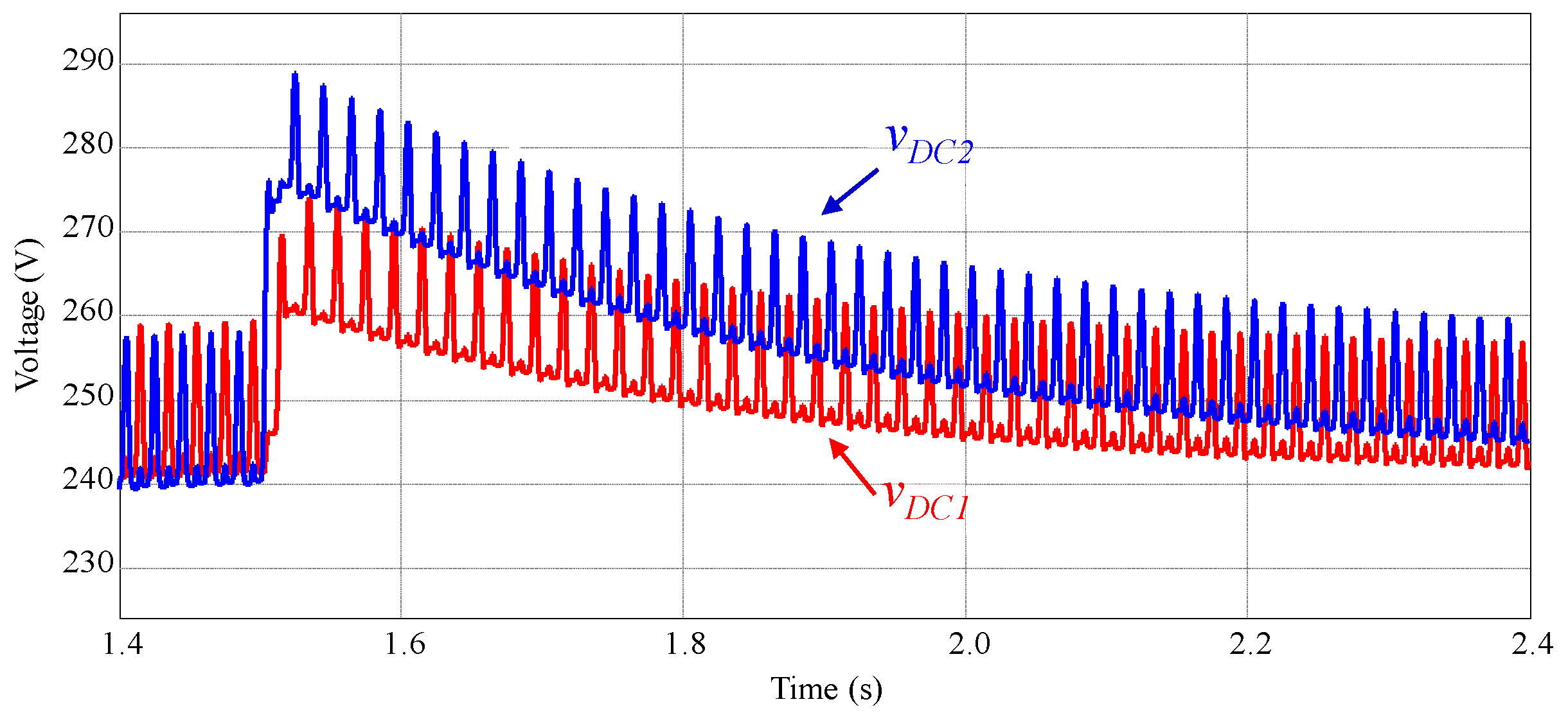
Figure 14 shows the SAPF response towards the connection of the second load at instant t = 1.5 s, where it can be seen that the source current presents a sinusoidal waveform even during the transient. The SAPF reference and output currents are also depicted, where an accurate current tracking can be perceived. On the other hand, Figure 15 shows the voltages in each DC-link capacitor. Due to the connection of a load, the DC-link voltage tends to decrease abruptly so that the SAPF can accurately perform the compensation. Despite the initial voltage deviation, the DC-link voltage control compensates the voltage error, whereby the reference value of 250 V is reestablished. This behavior in the DC-Link voltages results from de time delay need to obtain the average values of the power components defined by the p-q theory after the load transient. In this work, the determination of the average values is performed by sliding window average of one grid-cycle. This means that after one grid cycle the SAPF operates again in steady state. However, to prevent sudden variations in the source currents, the repositioning of the initial voltage in the DC-link capacitors is performed more slowly.
Figure 16 shows the SAPF response towards the disconnection of the diode rectifier with RL load at instant t = 1.5 s. It is noticeable that the source current presents a sinusoidal waveform during the transient and, once again, an accurate current tracking can be noted. The voltages in each DC-link capacitor can be seen in Figure 17. In this case, due to the disconnection of a load, the DC-link voltage increases so that the SAPF performs the compensation during the transient. The DC-link voltage control is also capable of compensating the overvoltage, with the reference value of 250 V being once again restored.
In order to facilitate the comprehension of the benefits provided by the SAPF operation, Table 2 presents a comparison between the RMS, THD and PF of the load and source currents with the SAPF compensation for both the linear (Section 4.3.1) and the nonlinear (Section 4.3.2) loads. As it can be seen, the RMS values decrease in the source current, as well as the THD values. On the other hand, the PF increases practically to unity, as expected with the SAPF operation.
5. Implementation of a Laboratorial Prototype of the SAPF
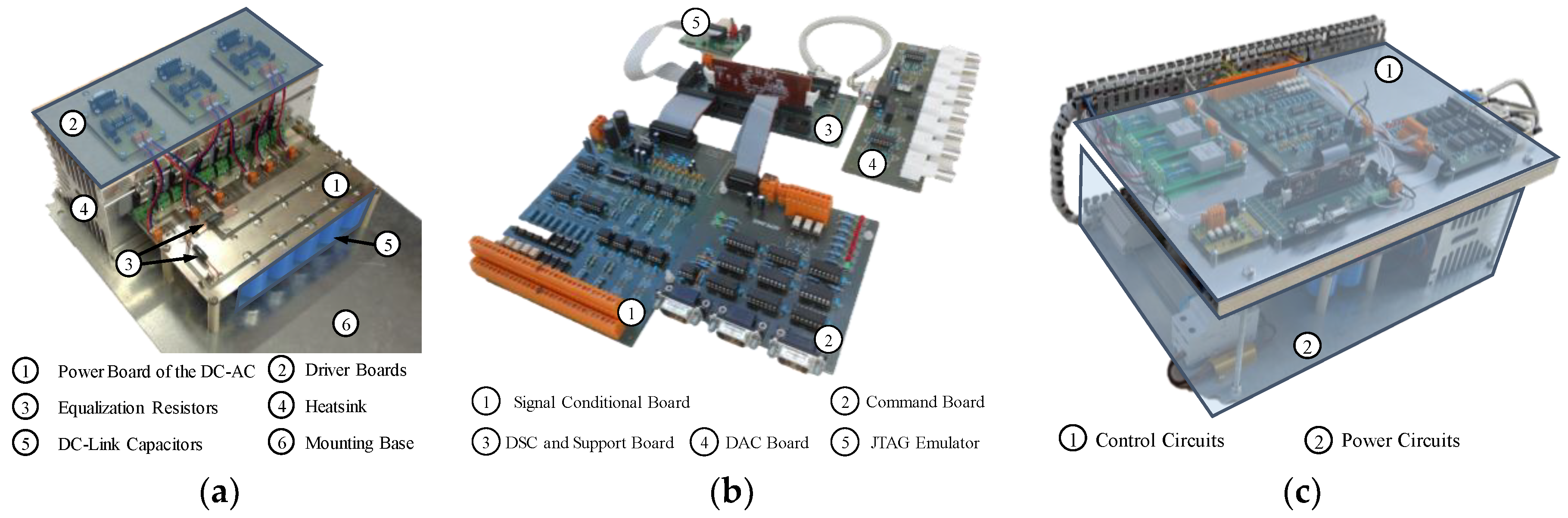
In this section, it is presented the developed hardware, as well as a description about the control algorithms for the proposed 5-level SAPF. In the SAPF it is possible to identify two main hardware circuits: the power circuits and the control circuits, as shown in Figure 18. The power circuits (Figure 18a) include several components, as the DC-link capacitors, the power switching devices, the gate driver boards, and the protection devices. Additionally, in the power circuit, it is also included the coupling inductor and the DC-link pre-charge system. On the other hand, the control circuit (Figure 18b) is constituted by a Digital Signal Controller (DSC), a connection board to access the pins of the DSC, a signal conditioning board to acquire the signals from the sensors, and by a command board. During the experimental tests, it was used a Digital-to-Analog Converter (DAC) board, not necessary for the functionality of the system, but very useful during the process of development and debugging of the control algorithms. Figure 18c shows the structure of the final prototype, constituted by two metallic mounting bases supporting all the hardware. In the first level are fixed all the components of the power circuit, and in the second level all the boards that constitute the control system. The structure and components disposition were sized, taking into account a posterior inclusion in an electric switchboard.
5.1. Power Circuit Hardware
In Figure 18a is presented the power circuit structure, where the 5-level converter was implemented, being possible to identify the heatsink, the power board of the 5-level converter, as well as the capacitors of the DC-link, the gate driver boards and a mounting base, where all the components are fixed. The IGBTs and diodes of the 5-level converter were fixed with the mounting clips that push them against the heatsink.
For each IGBT, a gate protection circuit was used, which consists of a 10 kΩ resistor in parallel with two 16 V zener diodes in series, with common anode. The gate protection is intended to protect the IGBTs gate terminals from voltage surges as well as to prevent unwanted switching. Additionally, in parallel with each complementary pair of IGBTs were placed snubber capacitors with the purpose of protecting the IGBTs from high voltage transients, which can occur when switching inductive loads.
The DC-link is composed of two sets of capacitors, which are placed in series and having the midpoint connected to the central point of the DCMLI. Each of them is charged with 250 V thus obtaining a voltage of 500 V on the DC-link. The use of a split DC-link is necessary to generate the different voltage levels of the converter. To generate these levels, it is possible to use the voltage of a single set of capacitors or the sum of the voltage of the two sets. For the proper operation of the 5-level converter, it is extremely important to maintain the same value of voltage in both sets of capacitors. Thus, in addition to the DC-link voltage balance control algorithm, an equalization resistor is placed in parallel with each set of capacitors, as it can be seen in Figure 18a. Each of the capacitor assemblies contains five electrolytic capacitors connected in parallel, each one with a value of 470 μF, thus obtaining a total of 2350 μF in each set of capacitors. These capacitors withstand a maximum voltage of 400 V.
The coupling of the 5-level converter to the power grid is done through two inductors and one DC-Link pre-charge system. This system consists of a pre-charge resistor in parallel with a bypass switch and a mains circuit breaker. The mains connection circuit breaker is responsible for connecting and disconnecting the SAPF with the power grid. The pre-charge resistor has the effect of limiting the initial current during the charge of the DC-link capacitors. The pre-charge bypass switch is used to create an alternative path for the current after the pre-charge. Whenever the mains circuit breaker is closed, the pre-charge system must be opened. The 5-level converter inductor consists of two windings with mutual coupling, where one is connected to the phase and the other is connected to the neutral. The two windings have an equivalent inductance of 1.6 mH. On the top of the heatsink, as shown in Figure 18a, the gate driver circuit boards are responsible for operating the IGBTs. In order to keep the control system galvanically isolated from the power stage, optical coupling driver circuits were used. Each board is capable of controlling two complementary IGBTs.
5.2. Control Circuit Hardware
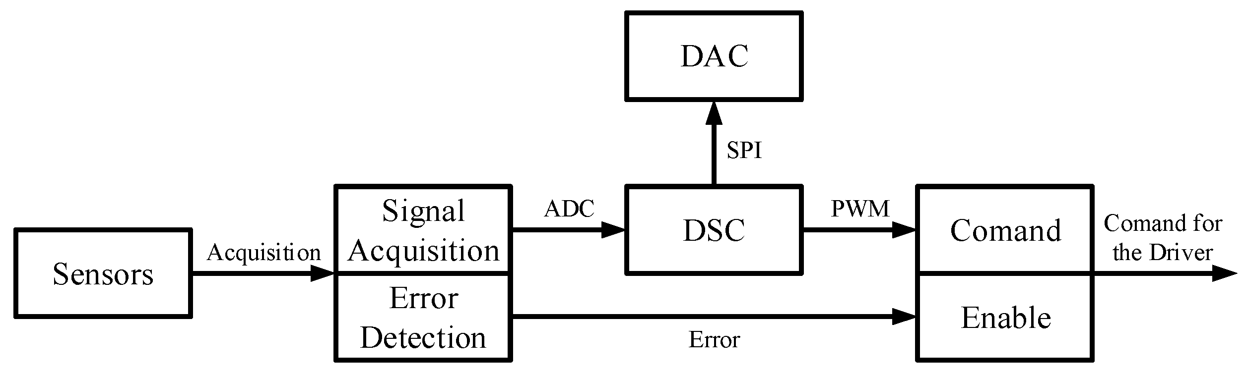
Figure 18b shows the boards responsible for the control system, from the acquisition of the voltage and current sensors signals to the generation of the PWM pulses that are applied to the gate driver boards described above. A block diagram of the control system is shown in Figure 19. This system consists of the block of sensors, followed by the block responsible for the signal conditioning and conversion of the analog signals to digital, through an Analog-to-Digital Converter (ADC). This block also contains a comparator circuit, used to detect if there exist values outside of the stipulated limits. The values converted by the ADC are made available to the DSC, where all the control algorithms were implemented. The DAC board connected to the DSC through a serial SPI communication allows a real-time visualization of the variables calculated by the control algorithms. Finally, the control block converts the PWM signals from the 3.3 V Transistor-Transistor Logic (TTL) to the 15 V Complementary Metal-Oxide Semiconductor (CMOS) logic used by the gate driver boards. This block also receives error signals, suspending the switching of all IGBTs in case any error is detected.
The signal conditioning board, previously presented in Figure 18b, is responsible to convert the analog signals into digital signals in order to enable the DSC to process the values acquired from the sensors. Although the DSC used in this project has an internal ADC, it presents some limitations. For this reason, a board with an external ADC was implemented. This ADC, manufactured by MAXIM with the reference MAX1320, can read 8 channels with bipolar input of ±5 V with a resolution of 14 bits. All the digital control algorithms of the system were implemented in the DSC, whereby in this work it is used the TMS320F28335 manufactured by Texas Instruments (Dallas, TX, USA). It is a platform with typical instructions of a Digital Signal Processor and with a set of peripherals typical of a microcontroller. This DSC has a 32-bit processor with a clock frequency up to 150 MHz with native support for floating-point operations, 16 channels of 12-bit ADC and 18 PWM channels. One important characteristic of the PWM module included in the DSC is the possibility to introduce a dead-time between the two complementary IGBTs of the converter leg, avoiding the existence of short circuits during the switching. Figure 20 shows a flowchart with the sequence of processes implemented in the DSC to perform the control system. After the peripheral configurations and variables initialization, the DSC enters in an infinite loop. There is a timer interrupt routine responsible to trigger the ADC start at every 25 μs resulting in a frequency of acquisition of 40 kHz. After the conclusion of the ADC conversion, it is implemented the routine responsible for the PLL algorithm, followed by the DC-link voltage control to calculate the required inputs of the p-q theory. The p-q theory routine determines the compensation current that is processed by the predictive current routine and, subsequently, by the SPWM strategy to determine the gate signals applied to the DSC PWM peripherals.
6. Experimental Results
In this section are presented and discussed the experimental results of the SAPF operating within different conditions. Before the final validation of the power converter operating as SAPF, all the circuits and control algorithms were validated in a step-by-step procedure to prevent damages of the prototype electronic components or the laboratory equipment. For safety reasons, the experimental results were obtained with a 50 V–50 Hz reduced voltage single-phase system. The installation used in the experimental tests was obtained from the low-voltage 230 V–50 Hz electrical grid using a 5.5 kVA step-down transformer with 9:2 voltage ratio.
6.1. Experimental Validation of the PLL Algorithm
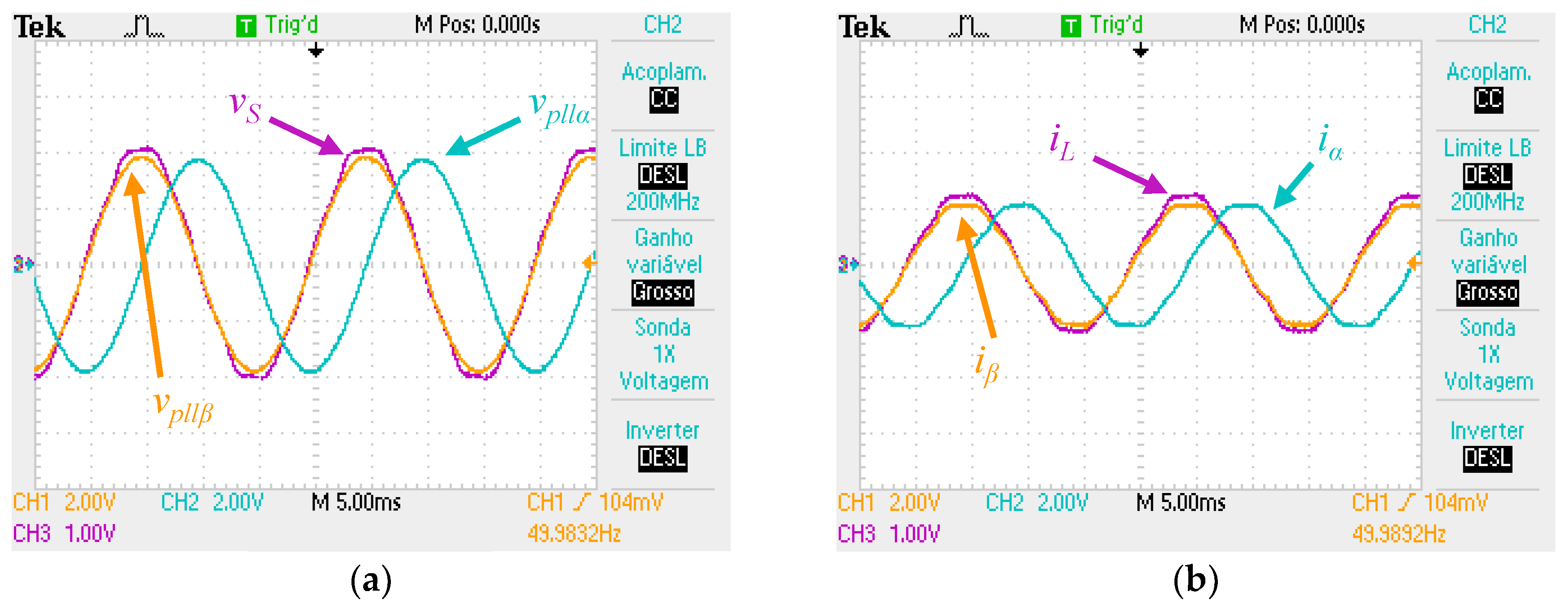
The preliminary tests began with the synchronization of the SAPF with the power grid. For this purpose, it was used a PLL algorithm responsible to detect the fundamental component of the source voltage. Figure 21a shows the source voltage (vS) and the PLL signal (vpll) calculated by the algorithm during the system connection. As it can be seen, the PLL algorithm quickly acquires the phase of vS, being the amplitude value achieved in a few grid-cycles. After the synchronization transient, the PLL signal (vpll) perfectly matches the fundamental component of vS as it can be seen in Figure 21b.
6.2. Experimental Validation of the p-q Theory
In this section are presented the experimental results from the p-q theory calculation. In the computer simulations, when implementing the p-q theory, the source voltage (vS) and the load current (iS) were used as the α coordinate, and a delay loop of 270° was implemented to obtain the β coordinate. However, in the experimental implementation, in order to increase the performance and save the DSC resources, it was chosen to keep the β coordinate as the original signal and delay the signals 90° to obtain the α coordinate. Subsequently, it is calculated the compensation current from the β coordinate current (iβ). The experimental implementation of the p-q theory algorithm applied to a single-phase installation is presented in Figure 22a shows the source voltage (vS) and the signals vα and vβ generated by the PLL algorithm. Figure 22b shows the current (iL) from a resistive load, as well as the generated signals iα and iβ. As previously mentioned, the phase shift between iα and iβ is achieved by the storage of the acquired current values into an array and posterior reading of the values with a 90° delay. In both cases, it is possible to see that the α coordinate has a delay of 90° related with the β coordinate.
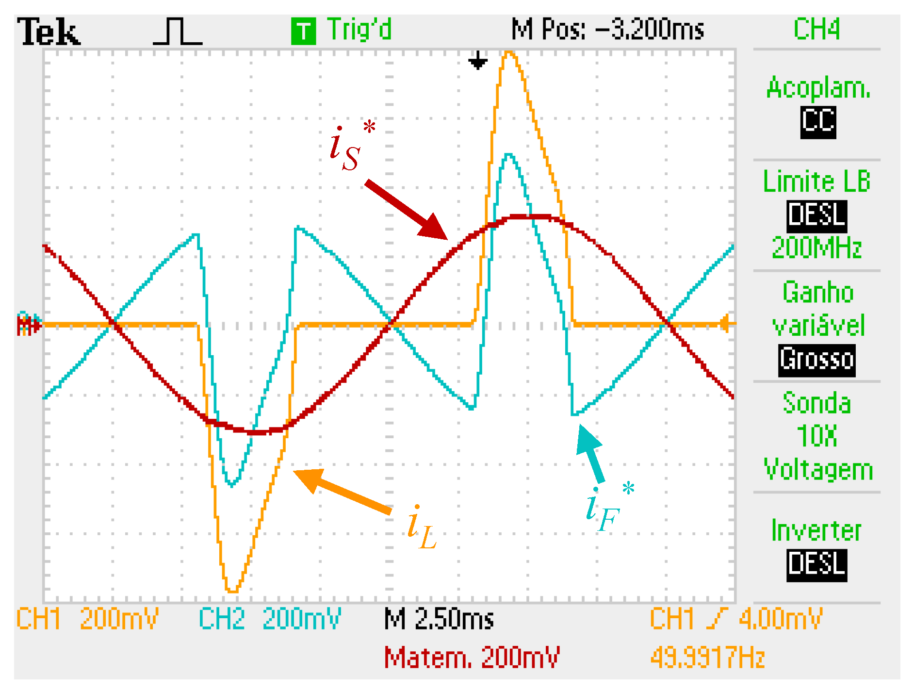
In order to test the p-q theory algorithms with non-linear loads, it was used a full-bridge diode rectifier with a resistor and a capacitor connected in parallel in the DC-side to calculate the compensation current and the theoretical value for the source current after compensation. Figure 23 shows the load current (iL), the compensation current calculated from the p-q theory (iF*), and the theoretical source current after the compensation (iS*). It can be seen that the theoretical source current (iS*), results from the difference between iF* with iL. Additionally, it can be seen that iS* is perfectly sinusoidal, validating the implemented p-q theory control algorithm.
6.3. Experimental Validation of the Modulation Technique
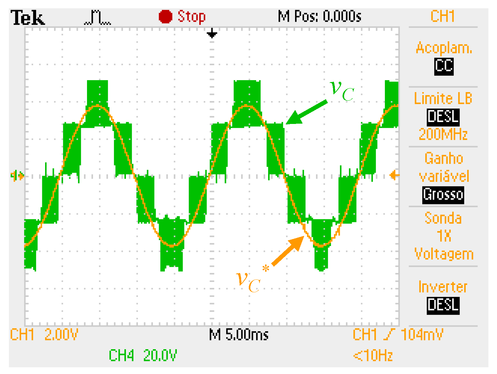
With the purpose of validating the modulation technique, it was used a sinusoidal waveform with 50 Hz as the reference to the modulation technique. In Figure 24, it is possible to see the voltage generated by the 5-level converter, as well as the sinusoidal reference. In this figure, the 5-levels generated by the power converter following the reference signal are clearly identifiable. For this experimental test, the 5-level converter was tested in open loop, with a DC power supply connected to the DC-link.
In order to avoid unnecessary commutations of the two-level leg of the 5-level converter, it was necessary to implement a hysteresis margin around the zero of the reference voltage, otherwise, due to the switching noise in the signals, several zero transitions can occur. To successfully mitigate this problem, it is necessary to consider a hysteresis band slightly higher than the noise.
6.4. Experimental Validation of the Predictive Current Controller
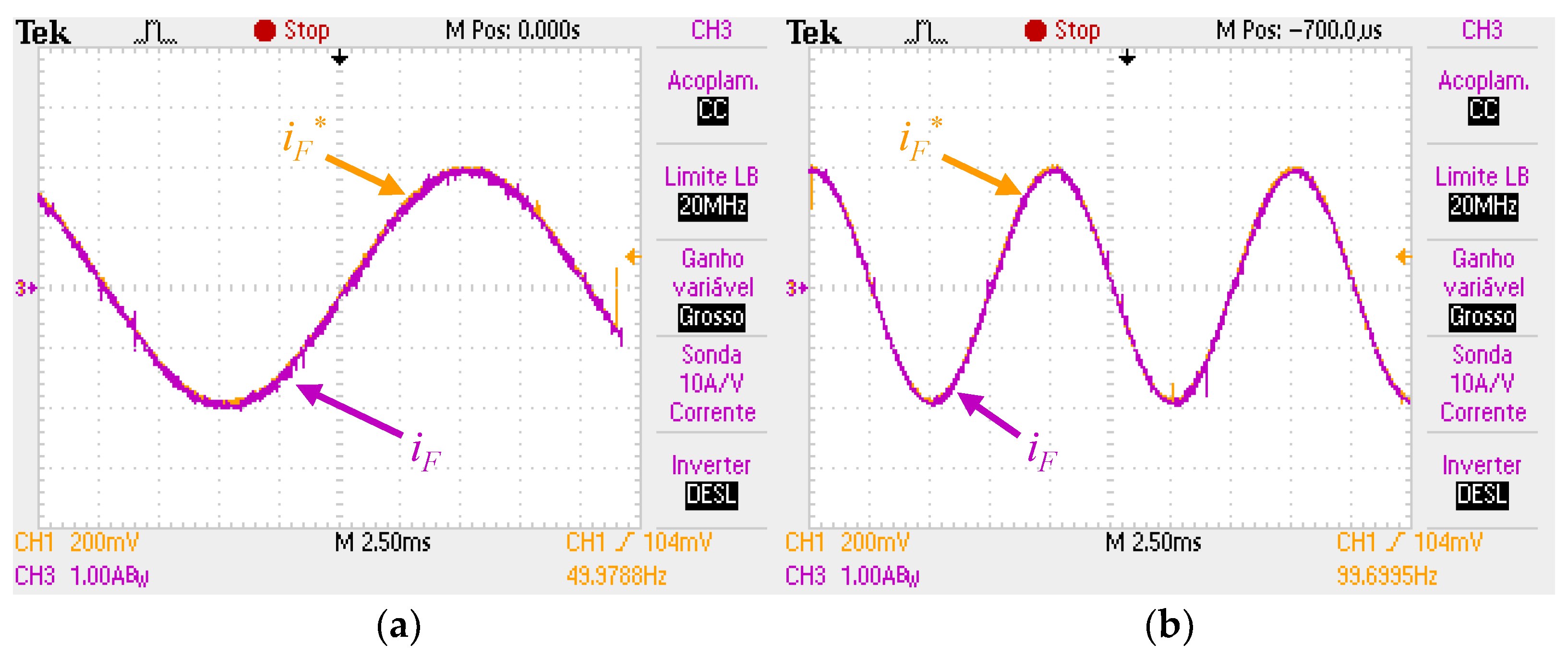
In order to test the predictive current control technique, it was used a resistive load in the output of the SAPF. With that, and once the 5-level converter is not connected to the power grid, the equation of the current control previously referred undergoes a slight change. In this way, the output voltage of the 5-level converter will correspond to the voltage in the output resistive load. During this test, the DC-link of the power converter is fed by two DC power supplies. In Figure 25 are presented the experimental results obtained with the predictive current control producing a sinusoidal current with 2 A of amplitude. Firstly, it was used a reference current with 50 Hz (Figure 25a), and in a second test was used a frequency equal to 100 Hz (Figure 25b). As it is possible to see in the figures, the filter current perfectly follows the references with a low switching ripple.
6.5. Experimental Validation of the DC-Link Voltage Controller
For a proper operation of the SAPF, the voltage on the DC-link should be slightly higher than the source peak voltage. To prevent a high peak current during the connection of the SAPF with the power grid, the pre-charge system described in the Section 5 needs to be operated correctly. As it can be seen in Figure 26, before the tests, the DC-link capacitors are fully discharged. When the SAPF is connected with the power grid, with the pre-charge system, at the time instant 1, the DC-link voltages start to increase until the peak value of the power grid voltage, approximately 70 V (35 V in each capacitor) and then at instant 2 the bypass contact is activated. A few seconds after, at time instant 3, the DC-link voltage control algorithm was enabled, starting to regulate the DC-link voltage to the reference value of 100 V (50 V in each capacitor). As it can be seen in the figure, the DC-link voltages converge to the reference value without any visible overshoot and maintaining the two voltages balanced, proving that the DC-link voltage control algorithm operates properly.
6.6. Experimental Results of the SAPF with RL Load
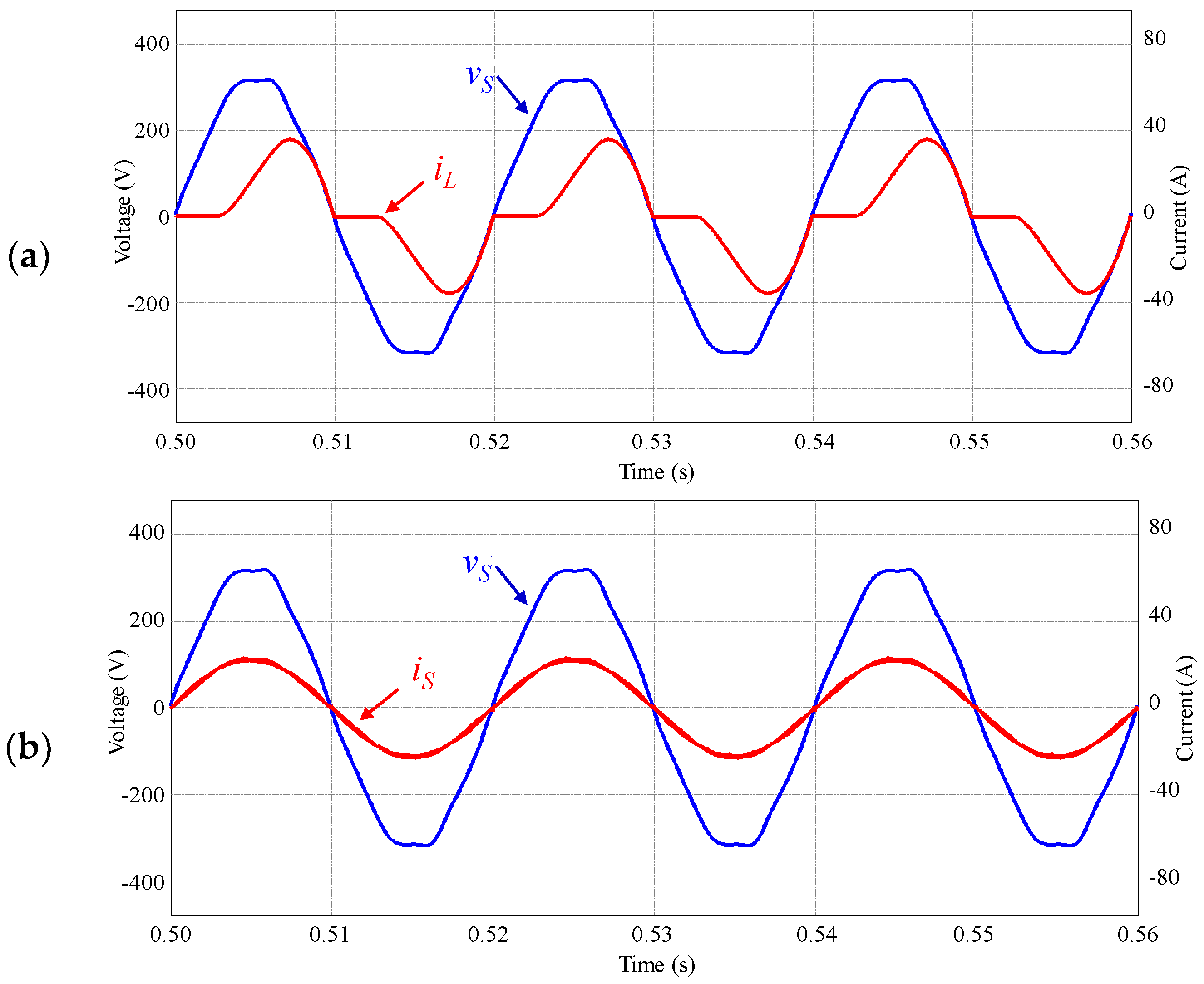
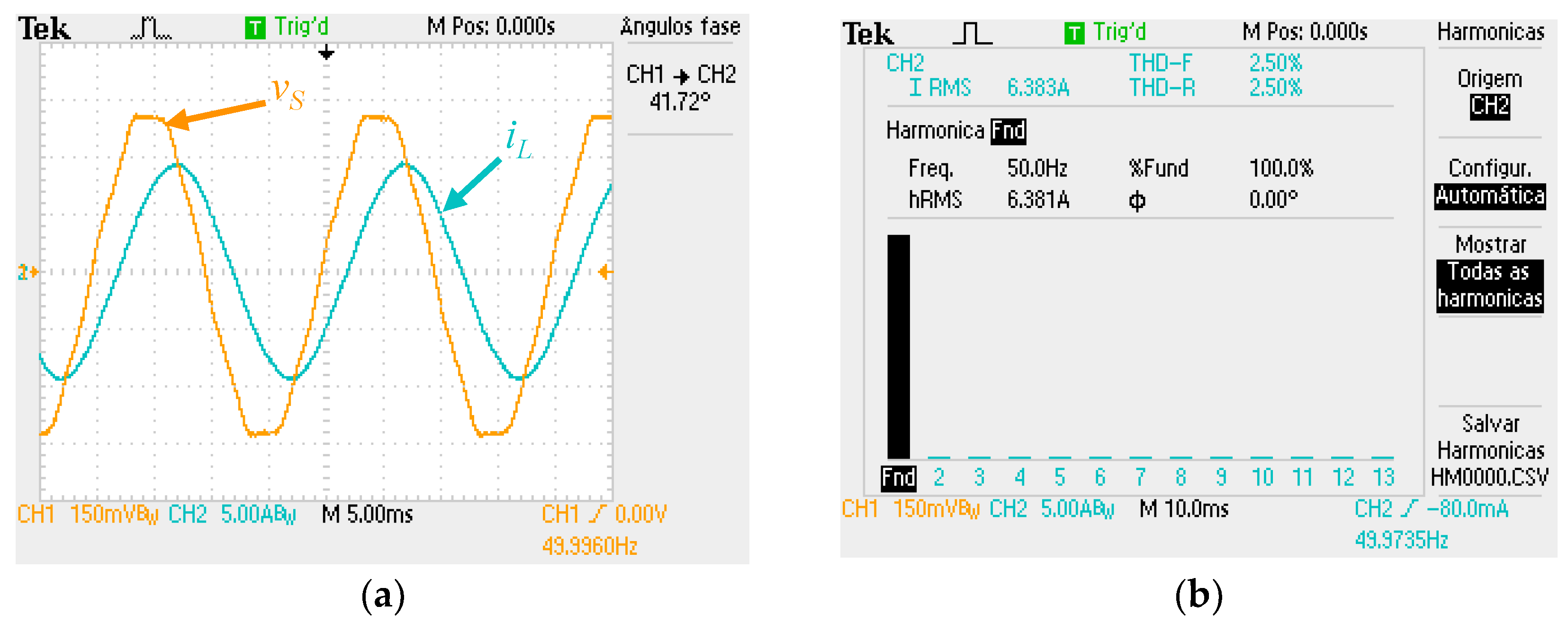
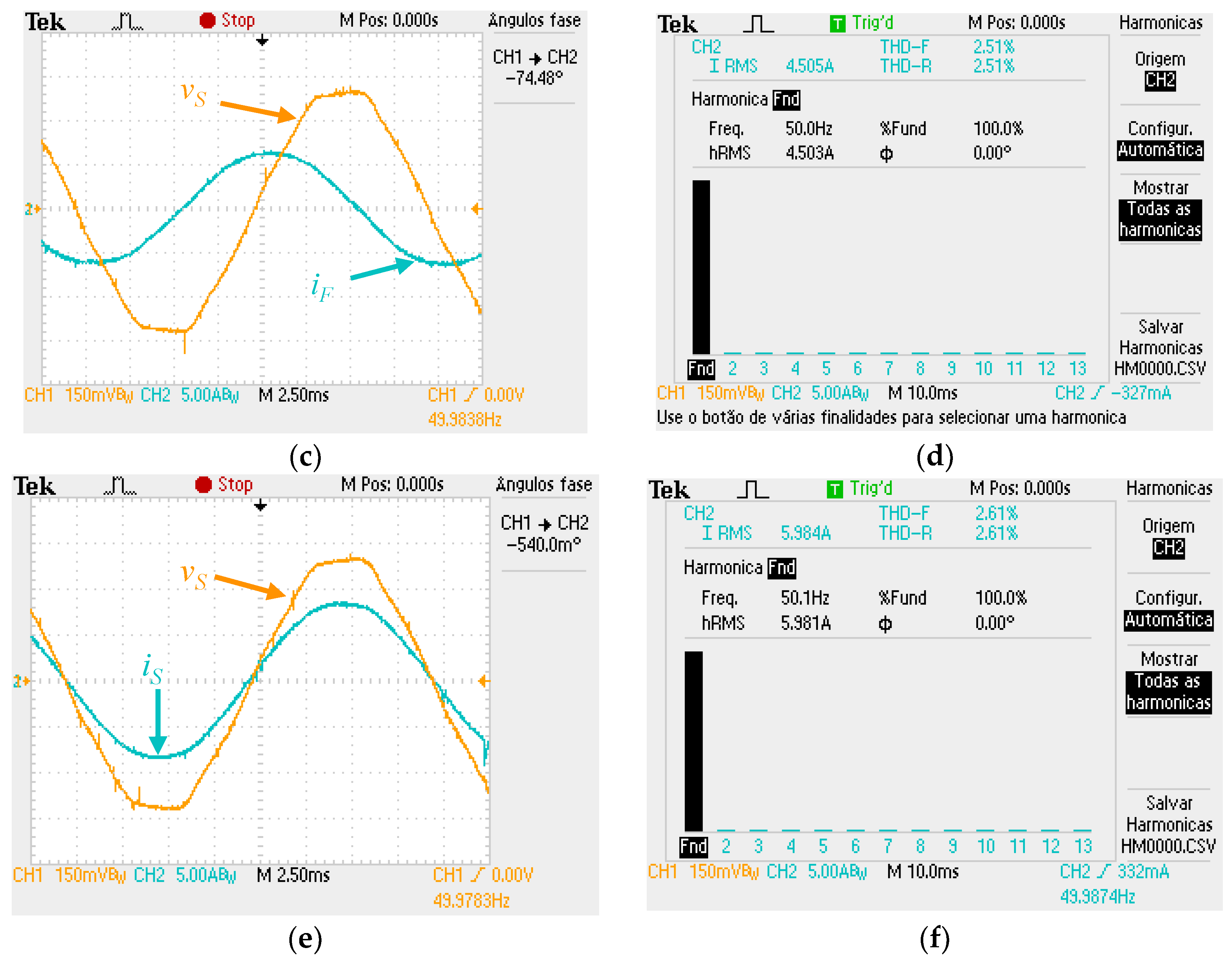
After validating the DC-link voltage control algorithm, the operation the SAPF was firstly tested with a linear load composed by a resistor in series with an inductor (RL load). The load current (iL) and the source voltage (vS) of the single-phase system are shown in Figure 27. In Figure 27a it is possible to see that iL and vS have a phase-shift of 42°, resulting in a PF of 0.74. Figure 27b is represented the harmonic spectrum of the load current, where it is possible to verify a THD of 2.5% and an RMS value of 6.4 A.
In order to compensate the reactive power of the RL load, the SAPF produces a current with a phase shift of 90° with the source voltage as shown in Figure 27c. After the compensation, the source current (iS) becomes sinusoidal and in phase with vS, as visible in Figure 27e. By consulting the Figure 27f, it is confirmed the phase shift of 0° of the fundamental component of the source current in relation to the source voltage, resulting in a PF of 0.99. It is also visible in Figure 27f that the RMS value of the source current is lower than the RMS value of the load current.
In Figure 27, it is visible that the source voltages, which correspond to the actual power grid voltages in the Power Electronics Laboratory, are not sinusoidal, due to distorted voltage drops in the line impedances caused by distorted currents of non-linear loads. Thus, the source voltages present a considerable amount of voltage harmonics. Nevertheless, the source currents after the SAPF compensation are almost perfectly sinusoidal. This result is only possible due to the used PLL, but also proves that the control algorithms are working as intended, allowing sinusoidal currents in the source to be obtainable.
6.7. Experimental Results of the SAPF with a Diode Rectifier with Capacitive Filter
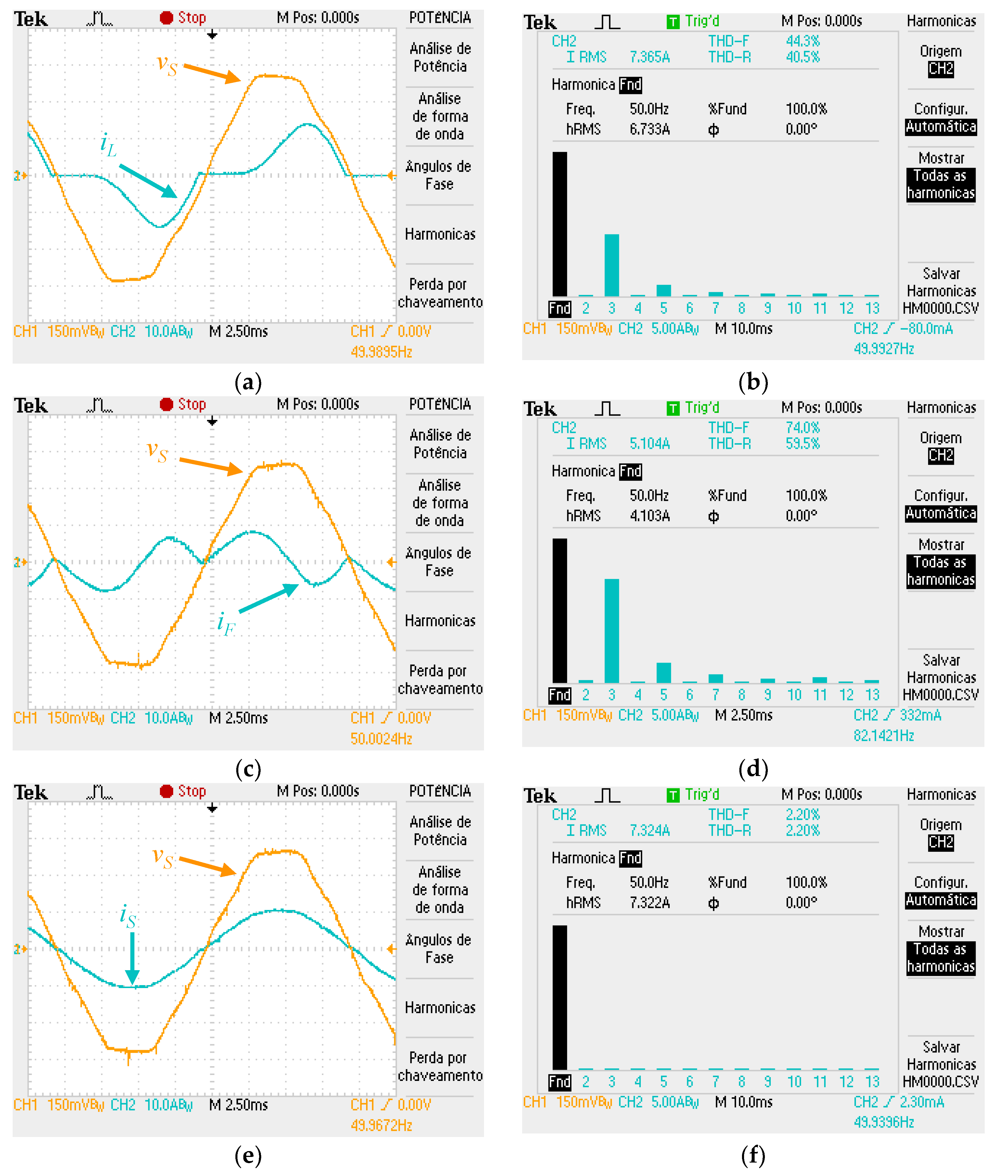
After the validation of operation with a linear load, the SAPF was tested with a non-linear load composed by a full-bridge diode rectifier with a resistor and capacitor connected in parallel in the DC-side. The results obtained during the test are presented in Figure 28. As expected, it is perfectly visible that the load current is distorted (Figure 28a), presenting a THD of 44% and an RMS value of 7.4 A (Figure 28b).
In Figure 28c, it is visible the compensation current produced by the SAPF (iF), as well as the harmonic spectrum in Figure 28d. Once again, and as desired, after the compensation the source current becomes sinusoidal and in phase with source voltage, as shown in Figure 28e. In Figure 28f, it is possible to verify that the THD of the current is reduced to a value of 2.2%. Table 3 presents the main indicators of the experimental results achieved with the SAPF. As it is possible to see, in both test cases, the RMS values of the source current are lower than the RMS values of the load currents. However, the benefits of the SAPF are more visible in terms of current harmonics and reactive power compensation. In both test cases the PF of the installation becomes almost unitary and in the case of the non-linear load, the THD is reduced from 44.3 to 2.2%.
7. Conclusions
A single-phase Shunt Active Power Filter (SAPF) based on a 5-level asymmetric full-bridge topology is proposed in this paper. Along the paper are presented the principle of operation of the 5-level power converter, the digital implementation of the p-q theory complemented by a Phase-Locked Loop and adapted to work with single-phase installations, the DC-link voltage control, the predictive current control and the multicarrier Sinusoidal Pulse-Width Modulation strategy. After the theoretical concepts, are described the simulation models and discussed the simulation results. A detailed description of a laboratory prototype implementation, including the sizing and selection of the electronic components is also presented, followed by a comprehensive description of the step-by-step hardware and control algorithms validation. Finally, the experimental results of the SAPF operating with linear and nonlinear loads are presented and discussed.
The simulation and experimental results confirm an excellent performance of the proposed SAPF topology and control algorithms, resulting always in a source current with very low Total Harmonic Distortion and in phase with the source voltage.
Despite the excellent results obtained, due to asymmetries of the full-bridge converter legs, mainly in terms of the switching frequency and maximum withstanding voltage, it may be interesting in a future work to combine the utilization of different semiconductor technologies. For instance, lower withstand voltage and fast switching technology (e.g., MOSFETs), and higher withstand voltage and slower switching technology (e.g., IGBTs) can be combined to implement a 5-level converter, which may result in interesting benefits in terms of efficiency and cost of the proposed solution.
Acknowledgments
This work has been supported by COMPETE: POCI-01-0145-FEDER-007043 and FCT—Fundação para a Ciência e Tecnologia within the Project Scope: UID/CEC/00319/2013. This work is financed by the ERDF—European Regional Development Fund through the Operational Programme for Competitiveness and Internationalisation—COMPETE 2020 Programme, and by National Funds through the Portuguese funding agency, FCT—Fundação para a Ciência e a Tecnologia, within project SAICTPAC/0004/2015-POCI-01-0145-FEDER-016434. Tiago Sousa is supported by the doctoral scholarship SFRH/BD/134353/2017 granted by the Portuguese FCT agency.
Author Contributions
José Gabriel Oliveira Pinto is the mentor of the idea of using the 5-level asymmetric full-bridge topology as a single-phase shunt active filter, participated in the development of the experimental prototype by designing some of the PCBs, and coordinated the organization and writing of the paper. Rui Macedo is the responsible for the implementation of the simulation model, hardware prototype, obtainment of the simulation results and experimental results, and participated in the writing of the paper. Vitor Monteiro participated in the design of the hardware prototype, sizing of electronic components, design of the predictive current control and writing of the paper. Luis Barros participated in the development of the hardware prototype, obtainment of the experimental results and writing of the paper. Tiago Sousa participated in the hardware prototype development, design of the SPWM modulation technique and writing of the paper. João L. Afonso participated in the design of the control algorithms based on the p-q theory, in the adaptation of the p-q theory to single-phase systems and in the writing of the paper.
Conflicts of Interest
The authors declare no conflict of interest.
References
- Dugan, R.C.; McGranaghan, M.F.; Santoso, S.; Beaty, H.W. Electrical Power Systems Quality, 3rd ed.; McGraw-Hill Education: New York, NY, USA, 2002. [Google Scholar]
- Balda, J.C.; Mantooth, A. Power-Semiconductor Devices and Components for New Power Converter Developments: A key enabler for ultrahigh efficiency power electronics. IEEE Power Electron. Mag. 2016, 3, 53–56. [Google Scholar] [CrossRef]
- Hoene, E.; Deboy, G.; Sullivan, C.R.; Hurley, G. Outlook on Developments in Power Devices and Integration: Recent Investigations and Future Requirements. IEEE Power Electron. Mag. 2018, 5, 28–36. [Google Scholar] [CrossRef]
- IEEE Recommended Practices and Requirements for Harmonic Control in Electrical Power Systems; 519-1992; IEEE: Piscataway, NJ, USA, 1993; pp. 1–112. [CrossRef]
- Palmer, J.A.; Degeneff, R.C.; McKernan, T.M.; Halleran, T.M. Pipe-type cable ampacities in the presence of harmonics. IEEE Trans. Power Deliv. 1993, 8, 1689–1695. [Google Scholar] [CrossRef]
- Faiz, J.; Ghazizadeh, M.; Oraee, H. Derating of transformers under non-linear load current and non-sinusoidal voltage—An overview. IET Electron. Power Appl. 2015, 9, 486–495. [Google Scholar] [CrossRef]
- Lee, K.; Carnovale, D.; Young, D.; Ouellette, D.; Zhou, J. System Harmonic Interaction Between DC and AC Adjustable Speed Drives and Cost Effective Mitigation. IEEE Trans. Ind. Appl. 2016, 52, 3939–3948. [Google Scholar] [CrossRef]
- Mendis, S.R.; Gonzalez, D.A. Harmonic and transient overvoltage analyses in arc furnace power systems. IEEE Trans. Ind. Appl. 1992, 28, 336–342. [Google Scholar] [CrossRef]
- Liu, Y.; Heydt, G.T.; Chu, R.F. The Power Quality Impact of Cycloconverter Control Strategies. IEEE Trans. Power Deliv. 2005, 20, 1711–1718. [Google Scholar] [CrossRef]
- Gomez, J.C.; Morcos, M.M. Impact of EV battery chargers on the power quality of distribution systems. IEEE Trans. Power Deliv. 2003, 18, 975–981. [Google Scholar] [CrossRef]
- Blanco, A.M.; Stiegler, R.; Meyer, J. Power Quality Disturbances Caused by Modern Lighting Equipment (CFL and LED). In Proceedings of the 2013 IEEE Grenoble Conference, Grenoble, France, 16–20 June 2013; pp. 1–6. [Google Scholar] [CrossRef]
- Peng, F.Z.; Akagi, H.; Nabae, A. A new approach to harmonic compensation in power systems-a combined system of shunt passive and series active filters. IEEE Trans. Ind. Appl. 1990, 26, 983–990. [Google Scholar] [CrossRef]
- Sasaki, H.; Machida, T. A New Method to Eliminate AC Harmonic Currents by Magnetic Flux Compensation-Considerations on Basic Design. IEEE Trans. Power Appar. Syst. 1971, PAS-90, 2009–2019. [Google Scholar] [CrossRef]
- Gyugyi, L.; Strycula, E.C. Active AC Power Filters. In Proceedings of the IEEE IAS Annual Meeting, Chicago, IL, USA, 11–14 October 1976; p. 529. [Google Scholar]
- Singh, B.; Al-Haddad, K.; Chandra, A. A review of active filters for power quality improvement. IEEE Trans. Ind. Electron. 1999, 46, 960–971. [Google Scholar] [CrossRef]
- Akagi, H.; Kanazawa, Y.; Nabae, A. Generalized Theory of the Instantaneous Reactive Power in Three-Phase Circuits. In Proceedings of the 1983 International Power Electronics Conference, Tokyo, Japan, 27–31 March 1983; pp. 1375–1386. [Google Scholar]
- Depenbrock, M. The FBD-method, a generally applicable tool for analyzing power relations. IEEE Trans. Power Syst. 1993, 8, 381–387. [Google Scholar] [CrossRef]
- Czarnecki, L.S. Orthogonal decomposition of the currents in a 3-phase nonlinear asymmetrical circuit with a nonsinusoidal voltage source. IEEE Trans. Instrum. Meas. 1988, 37, 30–34. [Google Scholar] [CrossRef]
- Bhattacharya, S.; Divan, D. Synchronous frame based controller implementation for a hybrid series active filter system. In Proceedings of the IAS ’95. Conference Record of the 1995 IEEE Industry Applications Conference Thirtieth IAS Annual Meeting, Orlando, FL, USA, 8–12 October 1995; pp. 2531–2540. [Google Scholar] [CrossRef]
- Hoon, Y.; Radzi, M.M.; Hassan, M.; Mailah, N. Control Algorithms of Shunt Active Power Filter for Harmonics Mitigation: A Review. Energies 2017, 10, 2038. [Google Scholar] [CrossRef]
- Pinto, J.G.; Exposto, B.; Monteiro, V.; Monteiro, L.F.C.; Couto, C.; Afonso, J.L. Comparison of current-source and voltage-source Shunt Active Power Filters for harmonic compensation and reactive power control. In Proceedings of the IECON 2012—38th Annual Conference on IEEE Industrial Electronics Society, Montreal, QC, Canada, 25–28 October 2012; pp. 5161–5166. [Google Scholar] [CrossRef]
- Lai, J.; Peng, F.Z. Multilevel converters-a new breed of power converters. In Proceedings of the 1995 Industry Applications Conference, Thirtieth IAS Annual Meeting, IAS ’95, Orlando, FL, USA, 8–12 October 1995; pp. 2348–2356. [Google Scholar] [CrossRef]
- Rodriguez, J.; Lai, J.; Peng, F.Z. Multilevel inverters: A survey of topologies, controls, and applications. IEEE Trans. Ind. Electron. 2002, 49, 724–738. [Google Scholar] [CrossRef]
- Nabae, A.; Takahashi, I.; Akagi, H. A New Neutral-Point-Clamped PWM Inverter. IEEE Trans. Ind. Appl. 1981, IA-17, 518–523. [Google Scholar] [CrossRef]
- Hochgraf, C.; Lasseter, R.; Divan, D.; Lipo, T.A. Comparison of multilevel inverters for static VAr compensation. In Proceedings of the 1994 IEEE Industry Applications Society Annual Meeting, Denver, CO, USA, 2–6 October 1994; pp. 921–928. [Google Scholar] [CrossRef]
- Teodorescu, R.; Blaabjerg, F.; Pedersen, J.K.; Cengelci, E.; Enjeti, P.N. Multilevel inverter by cascading industrial VSI. IEEE Trans. Ind. Electron. 2002, 49, 832–838. [Google Scholar] [CrossRef]
- Hasan, M.; Abu-Siada, A.; Islam, S.; Muyeen, S. A Novel Concept for Three-Phase Cascaded Multilevel Inverter Topologies. Energies 2018, 11, 268. [Google Scholar] [CrossRef]
- Reddy, K.B.M.; Pattnaik, S. Novel symmetric and asymmetric topology of multilevel inverter with reduced number of switches. In Proceedings of the 2017 IEEE International Conference on Industrial Technology (ICIT), Toronto, ON, Canada, 22–25 March 2017; pp. 165–170. [Google Scholar] [CrossRef]
- Elias, M.F.M.; Rahim, N.A.; Ping, H.W.; Uddin, M.N. Asymmetrical transistor-clamped H-bridge cascaded multilevel inverter. In Proceedings of the 2012 IEEE Industry Applications Society Annual Meeting, Las Vegas, NV, USA, 7–11 October 2012; pp. 1–8. [Google Scholar] [CrossRef]
- Dixon, J.; Moran, L. High-level multistep inverter optimization using a minimum number of power transistors. IEEE Trans. Power Electron. 2006, 21, 330–337. [Google Scholar] [CrossRef]
- Haddad, M.; Rahmani, S.; Hamadi, A.; Al-Haddad, K. New Single Phase Multilevel reduced count devices to Perform Active Power Filter. In Proceedings of the SoutheastCon 2015, Fort Lauderdale, FL, USA, 9–12 April 2015; pp. 1–6. [Google Scholar] [CrossRef]
- Martinez-Rodrigo, F.; Ramirez, D.; Rey-Boue, A.; de Pablo, S.; Lucas, L.H. Modular Multilevel Converters: Control and Applications. Energies 2017, 10, 1709. [Google Scholar] [CrossRef]
- Moranchel, M.; Huerta, F.; Sanz, I.; Bueno, E.; Rodríguez, F. A Comparison of Modulation Techniques for Modular Multilevel Converters. Energies 2016, 9, 1091. [Google Scholar] [CrossRef]
- Rolim, L.G.B.; da Costa, D.R.; Aredes, M. Analysis and Software Implementation of a Robust Synchronizing PLL Circuit Based on the pq Theory. IEEE Trans. Ind. Electron. 2006, 53, 1919–1926. [Google Scholar] [CrossRef]
- Karimi-Ghartemani, M. Linear and Pseudolinear Enhanced Phased-Locked Loop (EPLL) Structures. IEEE Trans. Ind. Electron. 2014, 61, 1464–1474. [Google Scholar] [CrossRef]
- Singh, B.N.; Khadkikar, V.; Chandra, A. Generalised single-phase p-q theory for active power filtering: Simulation and DSP-based experimental investigation. IET Power Electron. 2009, 2, 67–78. [Google Scholar] [CrossRef]
Figure 1.
Topology of the 5-level converter used in the Shunt Active Power Filter (SAPF).

Figure 2.
Block diagram of the DC-link voltage control algorithm.

Figure 3.
Block diagram of the predictive current control strategy implemented in the 5-level converter SAPF.
Figure 3.
Block diagram of the predictive current control strategy implemented in the 5-level converter SAPF.

Figure 4.
Adapted reference signal used in the modulation strategy.

Figure 5.
Sinusoidal Pulse-Width Modulation (SPWM) signals generation based on the adapted reference signals.
Figure 5.
Sinusoidal Pulse-Width Modulation (SPWM) signals generation based on the adapted reference signals.

Figure 6.
Block diagram of the 5-level converter SAPF control algorithms.

Figure 7.
Adapted reference signals used in the modulation strategy: (a) Ref2; (b) Ref1.

Figure 8.
Simulation results of the modified multilevel SPWM modulation technique: Converter reference voltage (vc*) and converter voltage (vc).
Figure 8.
Simulation results of the modified multilevel SPWM modulation technique: Converter reference voltage (vc*) and converter voltage (vc).

Figure 9.
Evolution of the DC-link voltages (vDC1 and vDC2) during the start-up of the SAPF.
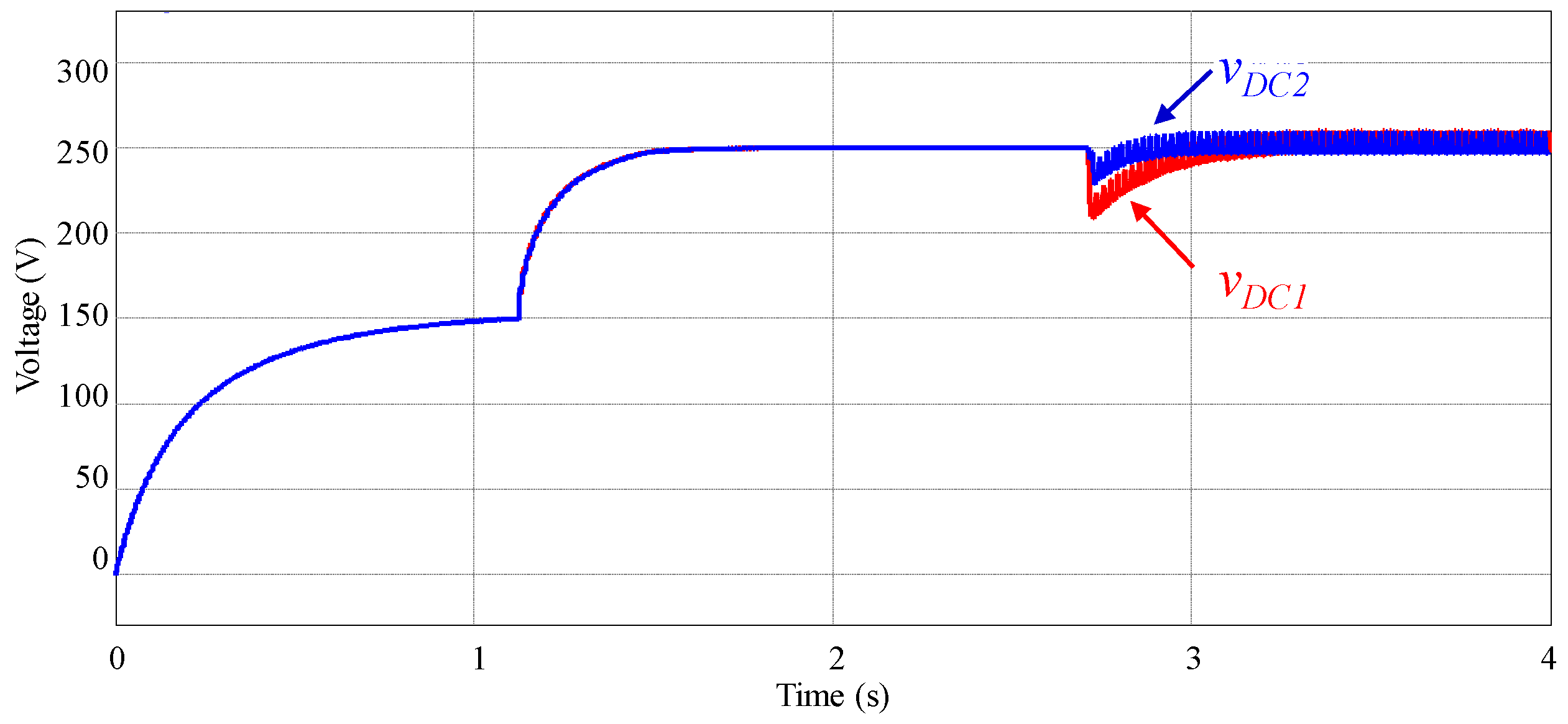
Figure 10.
Steady-state analysis of the SAPF operation with linear Resistive-Inductive (RL) Load: (a) Source voltage and load current; (b) Source voltage and source current.
Figure 10.
Steady-state analysis of the SAPF operation with linear Resistive-Inductive (RL) Load: (a) Source voltage and load current; (b) Source voltage and source current.

Figure 11.
Transient analysis of the SAPF starting of compensation with linear Resistive-Inductive (RL) Load.
Figure 11.
Transient analysis of the SAPF starting of compensation with linear Resistive-Inductive (RL) Load.

Figure 12.
Steady-state analysis of the SAPF operation with non-linear load: (a) Source voltage (vS) and load current (iL); (b) Source voltage (vS) and source current (iS).
Figure 12.
Steady-state analysis of the SAPF operation with non-linear load: (a) Source voltage (vS) and load current (iL); (b) Source voltage (vS) and source current (iS).

Figure 13.
Transient analysis of the SAPF operation with non-linear load: (a) Load (iL) and source currents (iS); (b) SAPF reference (iF*) and actual (iF) compensation current.
Figure 13.
Transient analysis of the SAPF operation with non-linear load: (a) Load (iL) and source currents (iS); (b) SAPF reference (iF*) and actual (iF) compensation current.

Figure 14.
Transient analysis of the SAPF operation with the connection of a non-linear load: (a) Load (iL) and source (iS) currents; (b) SAPF reference (iF*) and actual (iF) compensation current.
Figure 14.
Transient analysis of the SAPF operation with the connection of a non-linear load: (a) Load (iL) and source (iS) currents; (b) SAPF reference (iF*) and actual (iF) compensation current.

Figure 15.
Transient analysis of the SAPF DC-link voltages (vDC1 and vDC2) during the connection of a non-linear load.
Figure 15.
Transient analysis of the SAPF DC-link voltages (vDC1 and vDC2) during the connection of a non-linear load.
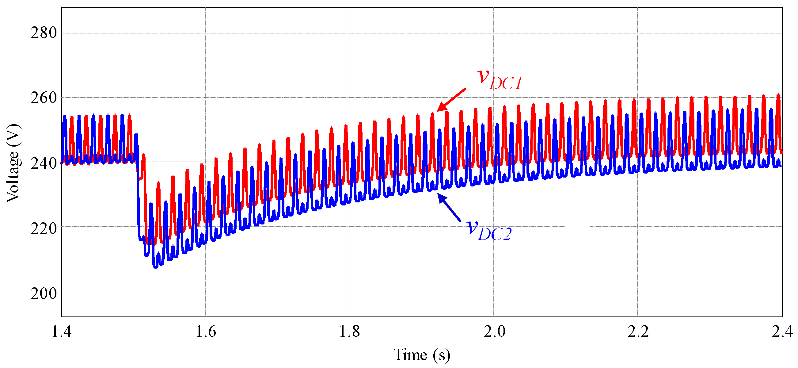
Figure 16.
Transient analysis of the SAPF operation with the disconnection of a non-linear load: (a) Load (iL) and source (iS) currents; (b) SAPF reference (iF*) and actual (iF) compensation current.
Figure 16.
Transient analysis of the SAPF operation with the disconnection of a non-linear load: (a) Load (iL) and source (iS) currents; (b) SAPF reference (iF*) and actual (iF) compensation current.

Figure 17.
Transient analysis of the SAPF DC-link voltages (vDC1 and vDC2) during the disconnection of a non-linear load.
Figure 17.
Transient analysis of the SAPF DC-link voltages (vDC1 and vDC2) during the disconnection of a non-linear load.

Figure 18.
Developed SAPF: (a) Power circuits; (b) Control circuits; (c) Final prototype.

Figure 19.
Block diagram of the control system.

Figure 20.
General flowchart of the control system implemented in the DSC.
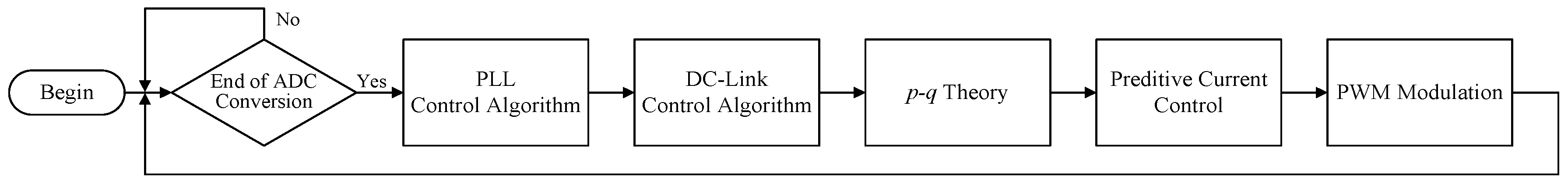
Figure 21.
Experimental results of the Phase-Locked Loop (PLL) control algorithm: (a) PLL synchronization transient; (b) PLL in steady state.
Figure 21.
Experimental results of the Phase-Locked Loop (PLL) control algorithm: (a) PLL synchronization transient; (b) PLL in steady state.
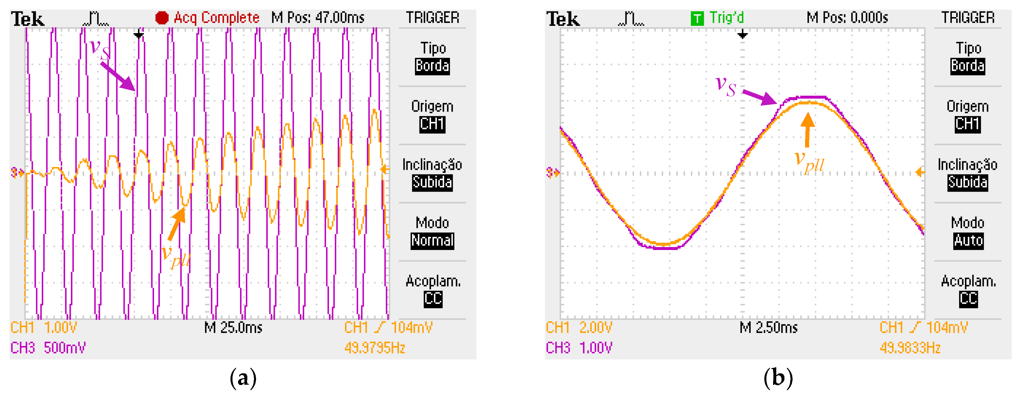
Figure 22.
Creation of a three-phase virtual balanced system from a single-phase installation for the application of the p-q theory: (a) Source voltage (vS) and PLL output signals in the α-β coordinates (vpllα and vpllβ); (b) Load currents in the α-β coordinates (iα and iβ).
Figure 22.
Creation of a three-phase virtual balanced system from a single-phase installation for the application of the p-q theory: (a) Source voltage (vS) and PLL output signals in the α-β coordinates (vpllα and vpllβ); (b) Load currents in the α-β coordinates (iα and iβ).

Figure 23.
Validation of the p-q theory algorithm with a full-bridge diode rectifier: Load current (iL), compensation current calculated by the p-q theory (iF*), and the theoretical source current after the compensation (iS*).
Figure 23.
Validation of the p-q theory algorithm with a full-bridge diode rectifier: Load current (iL), compensation current calculated by the p-q theory (iF*), and the theoretical source current after the compensation (iS*).

Figure 24.
Experimental results of the modified multilevel SPWM modulation technique: Converter reference voltage (vc*) and converter voltage (vc).
Figure 24.
Experimental results of the modified multilevel SPWM modulation technique: Converter reference voltage (vc*) and converter voltage (vc).

Figure 25.
Experimental validation of the predictive current control algorithm producing a sinusoidal current with 2 A of amplitude: (a) Sinusoidal current with 50 Hz frequency; (b) Sinusoidal current with 100 Hz frequency.
Figure 25.
Experimental validation of the predictive current control algorithm producing a sinusoidal current with 2 A of amplitude: (a) Sinusoidal current with 50 Hz frequency; (b) Sinusoidal current with 100 Hz frequency.

Figure 26.
Experimental validation of the DC-link voltages (vDC1 and vDC2) control algorithm.

Figure 27.
Experimental results of the SAPF with a RL load: (a) Source voltage (vS) and load current, (iL); (b) Harmonic spectrum of the load current; (c) Source voltage (vS) and filter current (iF); (d) Harmonic spectrum of the current of the filter current; (e) Source voltage (vS) and source current (iS); (f) Harmonic spectrum of the source current.


Figure 28.
Experimental results of the SAPF with a Resistive-Capacitive (RC) load and a rectifier: (a) Source voltage (vS) and load current (iL); (b) Harmonic spectrum of the load current (iL); (c) Source voltage (vS) and SAPF current (iF); (d) Harmonic spectrum of the SAPF current; (e) Source voltage (vS) and source current (iS); (f) Harmonic spectrum of the source current (iS).


Table 1.
Voltage levels that the 5-level converter can assume during the positive and negative half-cycles.
Table 1.
Voltage levels that the 5-level converter can assume during the positive and negative half-cycles.
| Voltage Polarity | S1 | S1’ | S2 | S2’ | S3 | S3’ | vc |
|---|---|---|---|---|---|---|---|
| vC > 0 | OFF | ON | ON | OFF | ON | OFF | vDC |
| OFF | ON | OFF | ON | ON | OFF | vDC/2 | |
| OFF | ON | OFF | ON | OFF | ON | 0 | |
| vC < 0 | ON | OFF | ON | OFF | ON | OFF | 0 |
| ON | OFF | OFF | ON | ON | OFF | −vDC/2 | |
| ON | OFF | OFF | ON | OFF | ON | −vDC |
Table 2.
Comparison of simulation results of the Root Mean Square (RMS), Total Harmonic Distortion (THD) and power factor (PF) values of the load current and source current with SAPF compensation, for operation with linear and nonlinear loads.
Table 2.
Comparison of simulation results of the Root Mean Square (RMS), Total Harmonic Distortion (THD) and power factor (PF) values of the load current and source current with SAPF compensation, for operation with linear and nonlinear loads.
| Installation Parameter | Linear Load | Non-linear Load | ||
|---|---|---|---|---|
| Source | Load | Source | Load | |
| Current (RMS) | 10 A | 21 A | 15.8 A | 20.2 A |
| Current THD (%f) | 1.6% | 0.5% | 2.8% | 38% |
| PF | 0.99 | 0.47 | 0.99 | 0.78 |
Table 3.
Comparison of experimental results of the RMS, THD and PF values of the load current and source current with SAPF compensation, for operation with linear and non-linear loads.
Table 3.
Comparison of experimental results of the RMS, THD and PF values of the load current and source current with SAPF compensation, for operation with linear and non-linear loads.
| Installation Parameter | Linear Load | Non-linear Load | ||
|---|---|---|---|---|
| Source | Load | Source | Load | |
| Current (RMS) | 6.0 A | 6.4 A | 7.3 A | 7.4 A |
| Current THD (%f) | 2.6% | 2.5% | 2.2% | 44.3% |
| PF | 0.99 | 0.74 | 0.99 | 0.81 |
© 2018 by the authors. Licensee MDPI, Basel, Switzerland. This article is an open access article distributed under the terms and conditions of the Creative Commons Attribution (CC BY) license (http://creativecommons.org/licenses/by/4.0/).
Share and Cite
MDPI and ACS Style
Oliveira Pinto, J.G.; Macedo, R.; Monteiro, V.; Barros, L.; Sousa, T.; Afonso, J.L. Single-Phase Shunt Active Power Filter Based on a 5-Level Converter Topology. Energies 2018, 11, 1019. https://doi.org/10.3390/en11041019
AMA Style
Oliveira Pinto JG, Macedo R, Monteiro V, Barros L, Sousa T, Afonso JL. Single-Phase Shunt Active Power Filter Based on a 5-Level Converter Topology. Energies. 2018; 11(4):1019. https://doi.org/10.3390/en11041019
Chicago/Turabian StyleOliveira Pinto, José Gabriel, Rui Macedo, Vitor Monteiro, Luis Barros, Tiago Sousa, and João L. Afonso. 2018. "Single-Phase Shunt Active Power Filter Based on a 5-Level Converter Topology" Energies 11, no. 4: 1019. https://doi.org/10.3390/en11041019
Note that from the first issue of 2016, this journal uses article numbers instead of page numbers. See further details here.