1. Introduction
The role of an efficient DC-DC converter in Internet of Things (IoTs) applications and electronic devices is important, while highly efficient power-management units are required for any electronic device in which the battery voltage is higher than the supply voltage. For today’s electronic systems, an enhancement of the regulatory performance and the area efficiency are required [
1]. Numerous research works on the DC-DC converter have been reported, with the focus of some of them comprising small-sized, low-cost, low-power-consuming modern portable electronic devices. These converters are usually equipped with an off-chip inductor for maximum efficiency, and it is expected that they can offer multiple output-voltage levels, which is why they are called single-inductor multiple output (SIMO) DC-DC converters. Due to advancement of circuit technology, the research area of the single-output concept has become saturated; however, several pieces of research have been completed in the area of analog-controller SIMO DC-DC converters as well. Also, system stability, poor cross regulation and flexibility are the main issues of SIMO converters to achieve excellent performance [
2,
3,
4,
5,
6]. Studies of the digital-controller converters can be found in [
7,
8], while the field-programmable gate array (FPGA), microcontrollers, and compact reconfigurable input output (cRIO) play key roles in the operation of the corresponding digital controller. In most DC-DC converters, a digital control is employed for the external microcontrollers, FPGAs, and cRIO modules [
9,
10]. By contrast, the designed on-chip digital compensator of this paper occupies a small area.
The conventional SIMO DC-DC Converter is shown in
Figure 1. Usually conventional SIMO DC-DC converter has large area because of several analog-to-digital converters (ADCs), error amplifiers, counters, memory components, and filter capacitors. In addition, when the switching frequency is low, the inductance will be high, which causes a large area. Along with other SIMOs, in [
11,
12] also, the same number of ADCs and outputs are used. In contrast, in this work, no counter and error amplifiers are used except for one bandgap reference (BGR).
The issues of the SIMO DC-DC converter were studied. Poor cross-load regulation, line regulation, a low current capability, and a large ripple are the major disadvantages of the SIMO converter compared with the conventional DC-DC converter, while the poor cross-load regulation and the line regulation are considered to be critical problems. To reduce the cross-regulation, various techniques have been presented [
13,
14,
15]. Furthermore, the relationship between the cross-regulation and the load-transient response is close [
15]. Upon the occurrence of a load transience, a current mismatch occurs between the inductor current and the total output-load current until the inductor current is settled by a feedback loop. During this time, the other outputs are affected by this unbalanced current that is caused by the output load transience.
Time-multiplexing is a basic approach in SIMO DC-DC converters. This concept is responsible for not allowing the outputs to couple with each other, which reduces the cross-regulation effectively [
13,
16]. On the other hand, to add more outputs, the output power is reduced by multiple charging cycles per switching period in consequence and again the outputs require individual charging. To decrease the switching loss, ordered power distributive control (OPDC) has been proposed. The concept of power distributive approaches [
14,
17] decreases switching losses than the SIMO converters proposed in [
13,
16]. However, ADCs, digital controllers and counters, error amplifiers, external memories, reference voltage sources, large filter capacitors, and higher inductances that can lower switching frequencies require a large area. To avoid so many blocks, [
18] presents smooth loop handover (SLH) technique, solving the problems of close loop performance in digitally controlled SIMO converters. However, because of the use of a conventional delay cell in [
18], the die area is very large. Also, the number of outputs of this architecture is limited up to two.
This work presents a SIMO DC-DC converter with an interlaced hysteresis delay cell (IHDC)-topology using digital pulse-width modulation (DPWM) that is highly efficient and comprises a small area; furthermore, the transistor sizes are smaller than those of the conventional delay cells [
19]. In addition, the proposed architecture is extendable up to N outputs. DPWM plays a key role in terms of the digital controllers that convert the digital-limiter code to duty cycles. As area is a key factor of electronic devices, it was not used for both [
18] and this work. In [
16], a SIMO converter was designed having a share control loop in the analog domain. On the other hand, in this architecture feed-back control is used in the digital domain based on loop handover (LHO) topology.
In [
20,
21], the scheme of SLH is used only in analog domain, but in [
22], the scheme can apply in SIMO architectures with a digital control. This scheme is the best solution for the issues of the close loop that occur in DPWM SIMO DC-DC converters.
The rest of the paper continues as follows: the architectures of the DPWM SIMO DC-DC converter and the proposed IHDCs based on DPWM are explained in
Section 2.
Section 3 shows the experimental and measurement results. Finally, brief conclusions are given in
Section 4.
2. Architecture of DPWM SIMO DC-DC Converter
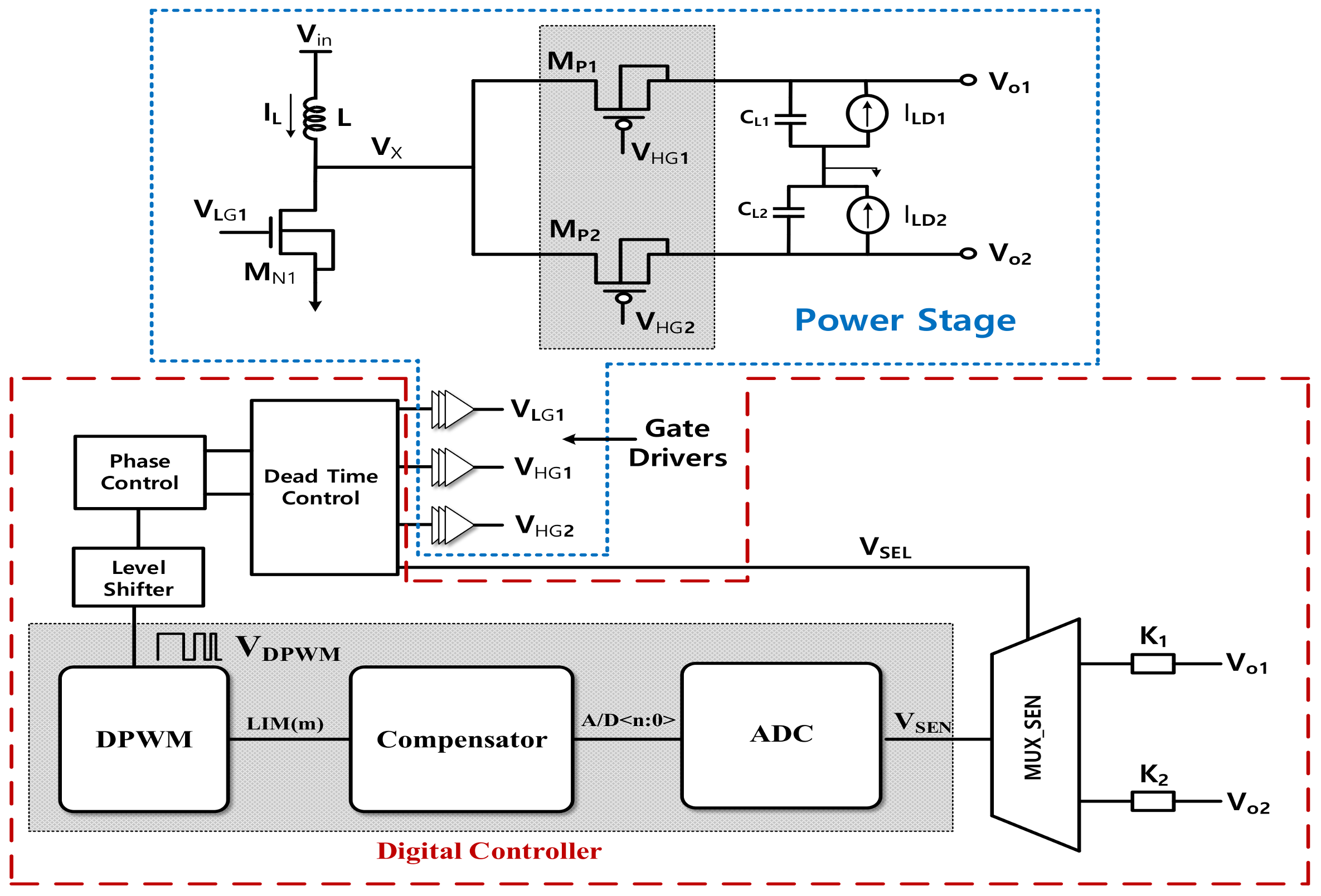
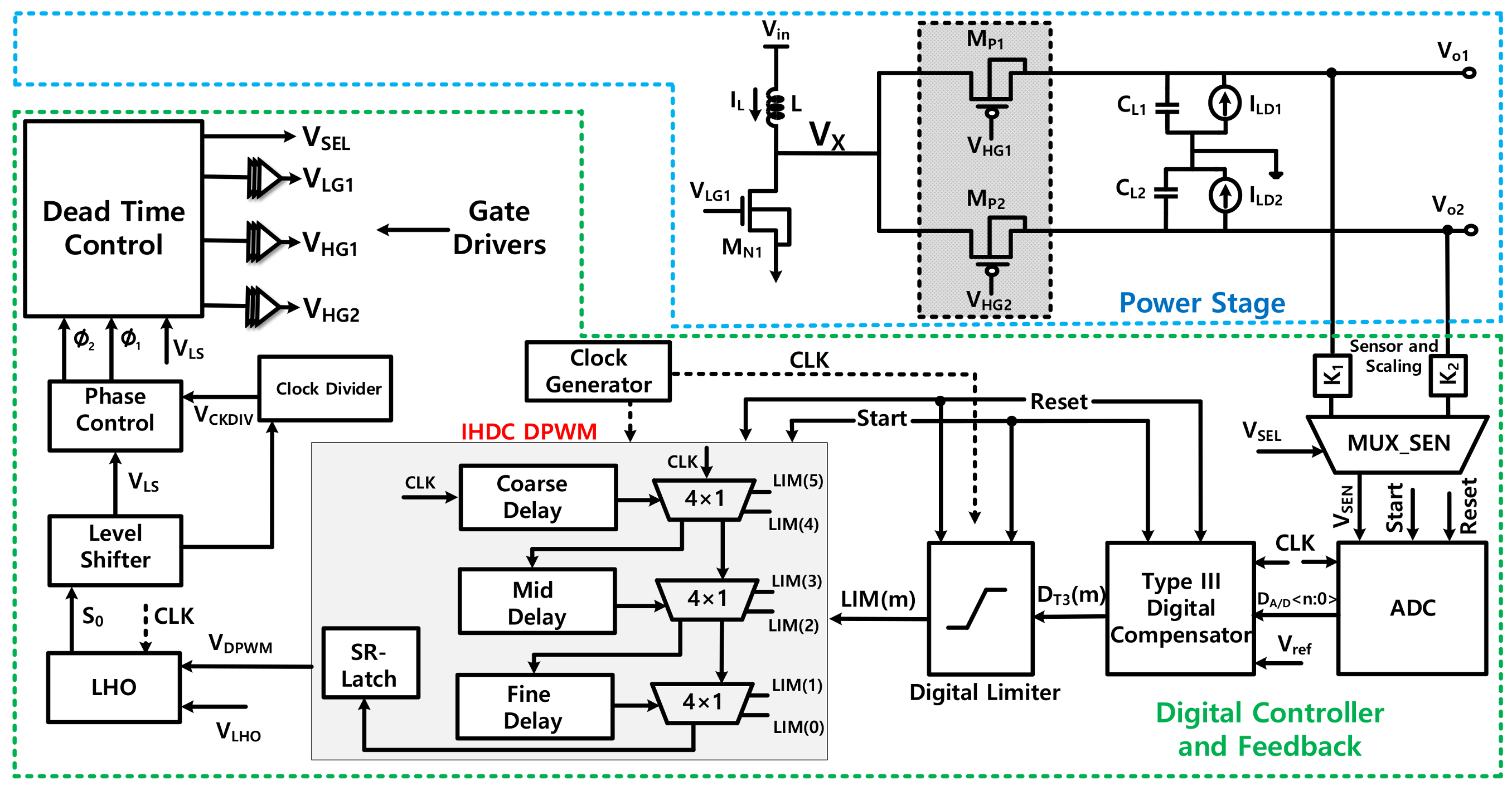
The proposed configuration of the present paper is composed of an IHDC-based DPWM, a Type-III digital compensator, a SIMO power stage, scaling and multiplexing, and a digital feedback controller, as shown in
Figure 2. In the proposed technique, the use of IHDCs has advantage of large delay, low power loss and small size over conventional delay cells; this IHDC-based DPWM scheme is explained in
Section 2.2.2. The proposed architecture is designed for two different output voltages, so the output fluctuations depend on the instantaneous energy present in the inductor and the feedback-resistance values for each output.
The proposed architecture does not require many reference voltages (Vref); it has only one (Vref). To get different feedback voltage, the value of the feedback resistances should be different. The fluctuation can be decreased, if the amount of inductor charge is enough before the load changes at Vo1. On the other hand, in the case of an inadequate energy value, because of different resistance values, the inductor must be charged and discharged for a relatively long duration of time.
When the power transistor M
N1 is on, the inductor is charged. In the next phase, however, the M
N1 is off and the M
P1 is on for the transferal of the energy that is stored in the inductor to V
o1; furthermore, this cycle is repeated for V
o2 as well, and a detailed description with a timing diagram is provided. This phenomenon of the control stage is explained in
Section 2.2.
Vo1 and Vo2 are provided as the multiplexer (Mux_SEN) inputs. The term fs/n selects each output, the fs represents switching frequency while n shows the number of outputs, which is converted by ADC into digital data. After that it is fed to Type-III digital compensator.
To avoiding overlapping, the digital limiter masks are designed to allow only the data that can be used, while the rest of the data are masked. These data can be converted into duty cycle by the DPWM. At the beginning, the LHO block is protected from affected input data provided by the DPWM. After a pre-specified time, the loop is completed in the tracking mode to achieve stability when the desired output-voltage levels are met. The clock divider helps to get fs/n frequency from the original source fs. The purpose of this action is to get a phase number that is the same number of outputs. Gate drivers are fed by phase control which is connected to P-type Metal Oxide Semiconductor (PMOS) power transistors MP1 and MP2, while the VLG1 bypasses the phase controller.
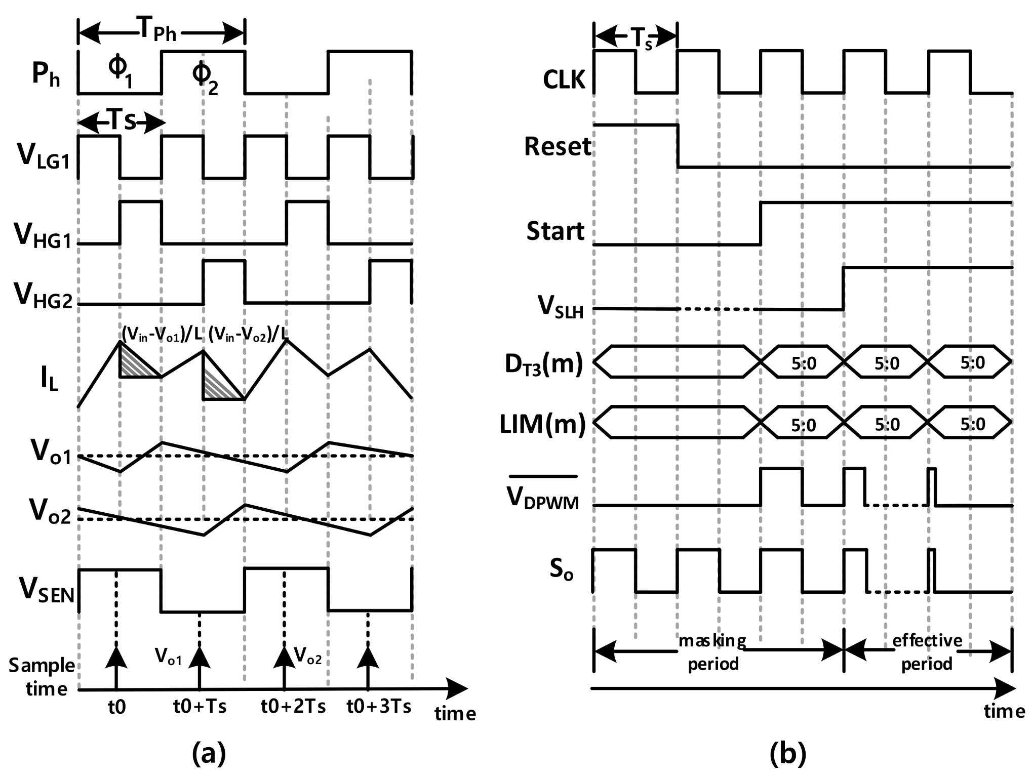
Figure 3a shows the timing diagram for the power stage, where V
LG1 is the M
N1 driving signal with the time period Ts, and P
h is the phase-control signal with T
Ph = 2(Ts). To keep the resistance minimum, widths (W) should be large like (WM
P1, M
P2) ≥ 2 × WM
N1. The efficiency decreases by increasing the difference between the input and the output. To avoid a big difference, the input voltage should be slender, lower than the selected low output-voltage levels. The power transistor M
N1 is switched on for a total of n times in one MPn time period, where n is the number of outputs. The M
N1 switched-on time is dictated by the controller feedback depending on the previous voltage levels at the V
o1 and V
o2 outputs.
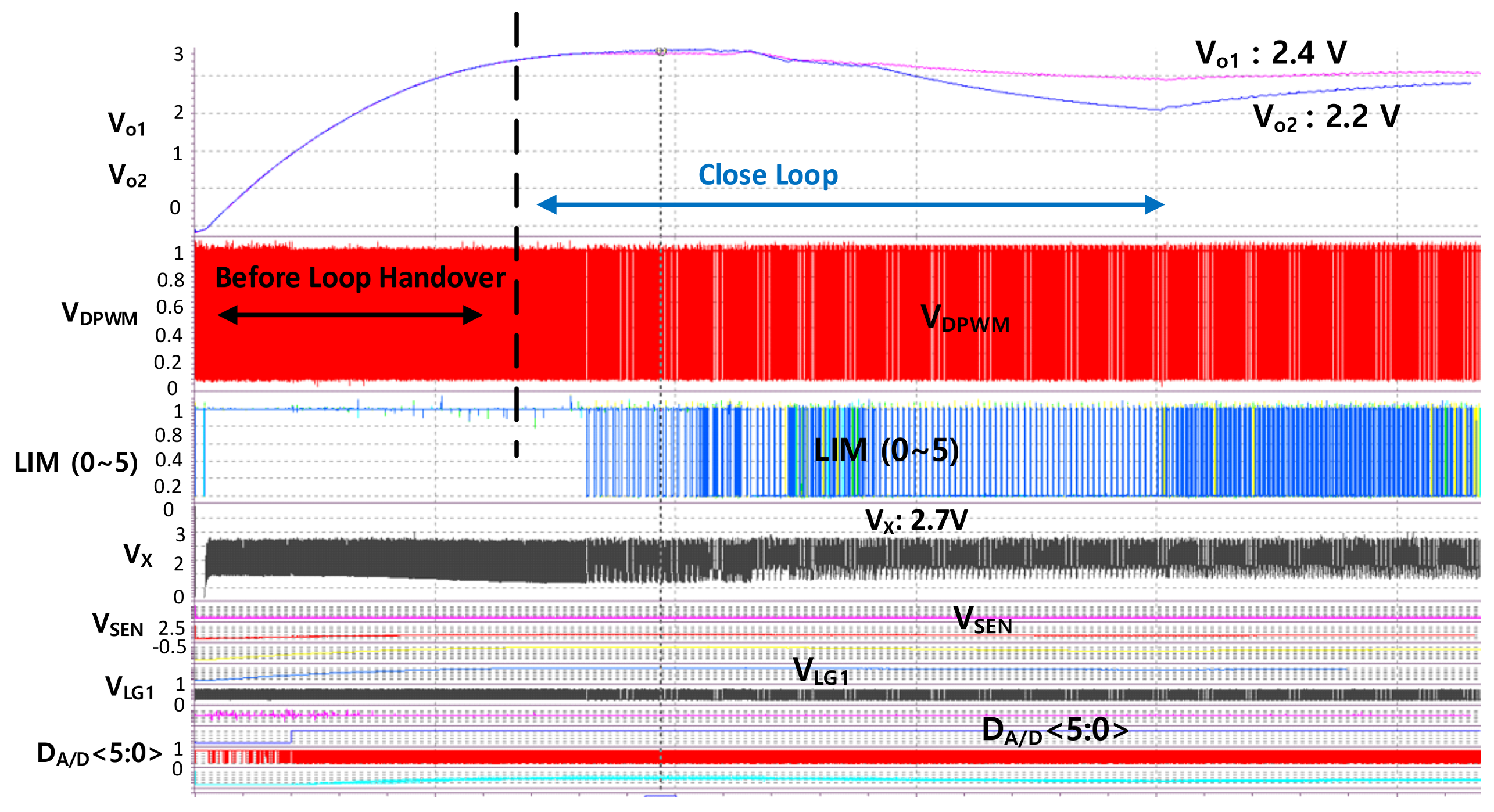
Figure 3b shows the timing diagram of the digital stage. At the start, D
T3(m), LIM(m) and inverted DPWM are reset. After the start signal they become active. Until the LHO signal is low, any output D
T3(m) from the digital stage is masked, as shown with the masking period. Ideally, the DPWM resolution should be greater than or equal to that of the Type-III digital compensator, which can be greater than or equal to that of the ADC to avoid limit cycling.
To save area and power consumption, a six-bit resolution is added to this architecture. In this work, to overcome the redundancy of the composter, ADC and DPWM, one control loop is shared by both outputs which has a benefit of low cost and small area. For VSEL = 0, the feedback for Vo1 output is processed through the control stage at phase Φ1. Likely, for VSEL = 1, the feedback for Vo2 output is processed through the control stage at phase Φ2.
Both feedback output voltages take a sampling duration 1/(fs/n) = (1/(5 MHz/2) = 400 ns). A scaled-down Vo1 is sampled at t0, t0 + 2Ts, t0 + 4Ts, …, and Vo2 is sampled at t0 + Ts, t0 + 3Ts, t0 + 5Ts, … For excellence accuracy, the control design band width which is equal to 5MHz is used. For gains these equations can be used K1 = Vref/Vo1, K2 = Vref/Vo2.
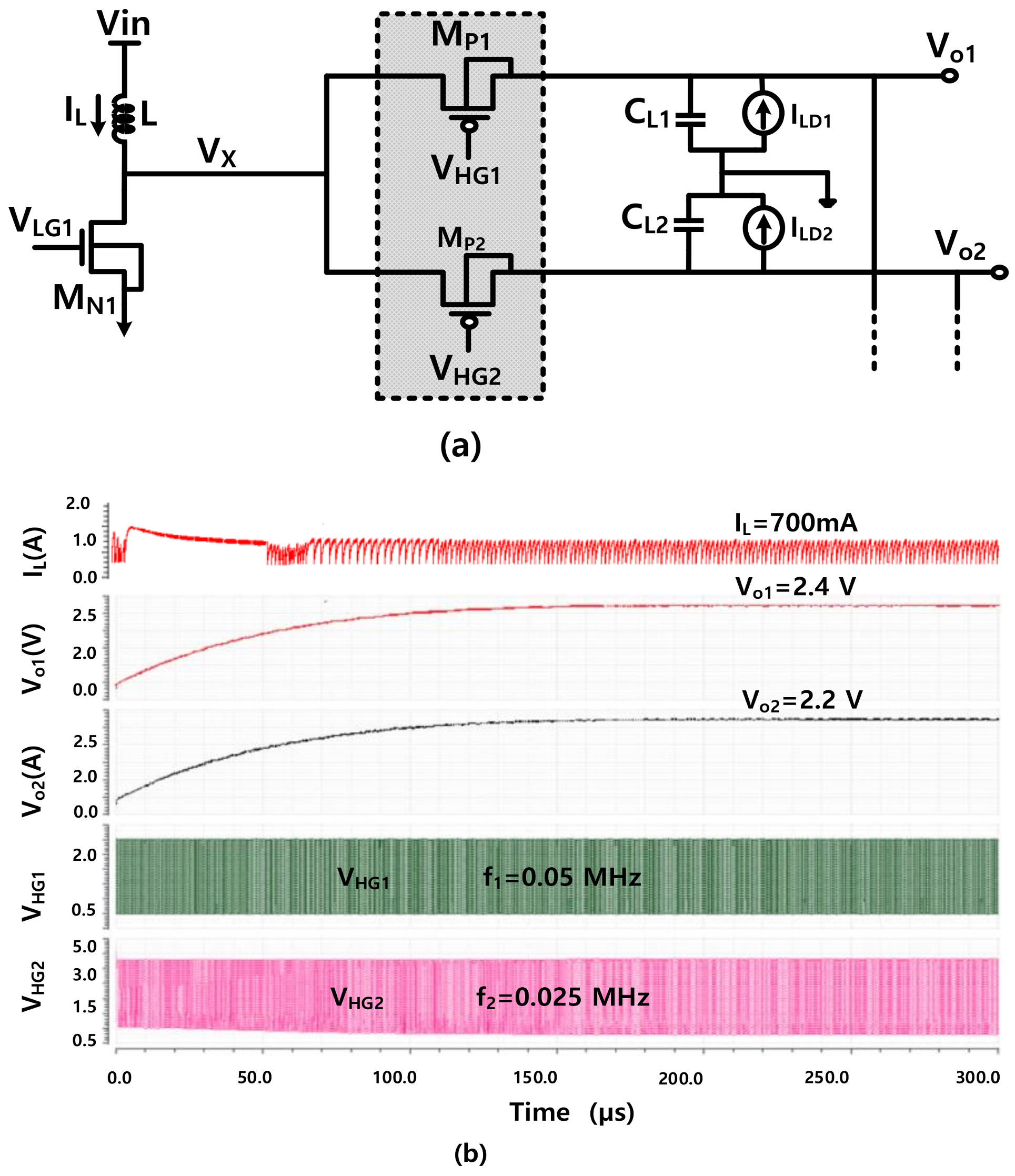
2.1. SIMO Power Stage
Figure 4a presents the SIMO power stage. When M
N1 is on and M
P1 and M
P2 are off, the inductor L charges with the input voltage (V
in)/L slope, whereas when M
P1 is on at the rate of (V
in − V
o1)/L, it discharges together with the V
in to V
o1. In the second phase, the slope of V
o2 is calculated as (V
in − V
o2)/L; therefore, the discharging of the inductor energy is alternatively transferred to the available outputs. The difference between the input and output voltages is inversely proportional to efficiency. So, a small difference is preferred; for this purpose output voltages should be choosen that are slender greater than the input. The switched-on time of the M
N1 is dictated by the controller feedback depending on the previous voltage levels at the V
o1 and V
o2 outputs. V
o1/K
1 and V
o2/K
2 are scaled-down signals from the sensors K
1 and K
2. ADC is fed by Mux_SEN V
SEN that are connected to ADC as an input. By energy transfer, the voltage ripple at V
o1 increases and then decreases by energy shifting to the next output. The simulation results are shown in
Figure 4b.
2.2. SIMO Control Stage
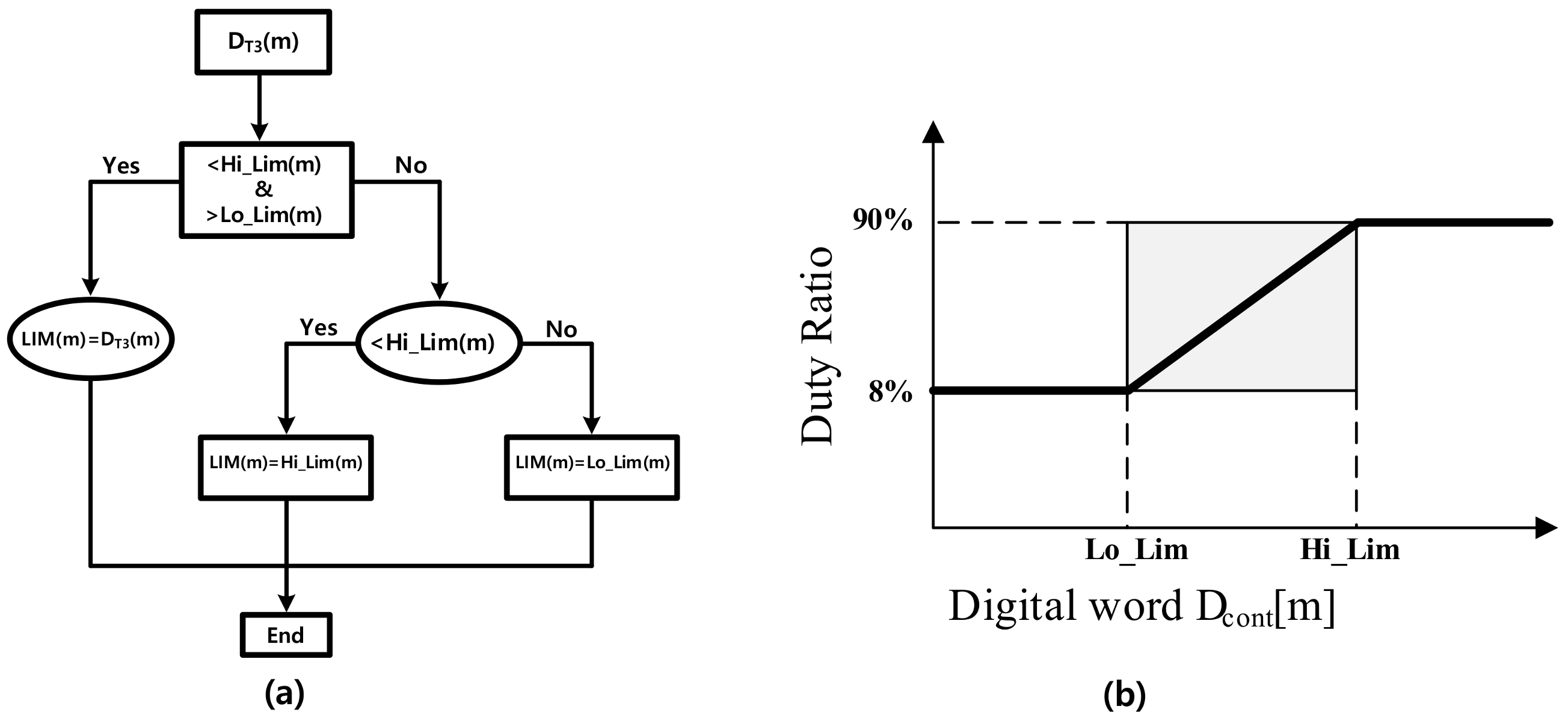
2.2.1. Digital Limiter
Only the data that must result in a duty-cycle in the range from 5–90% are allowed by the digital limiter, while the rest of the data are masked. A six-bit word Hi-Limit and Lo-Limit set the digital-limiter window.
Figure 5 show the flowchart and effective region of digital limiter.
As the input word, the Type-III digital compensator fed DT3(m) is compared to the predefined Hi-Limit and Lo-Limit. The output LIM(m) will be equal to input by inserting the input word in the Limit. On the other hand, if the input is higher than the Hi-Limit or less than the Lo-Limit, the output becomes either the Hi-Limit or the Lo-Limit, respectively, through the ignoring of the input word.
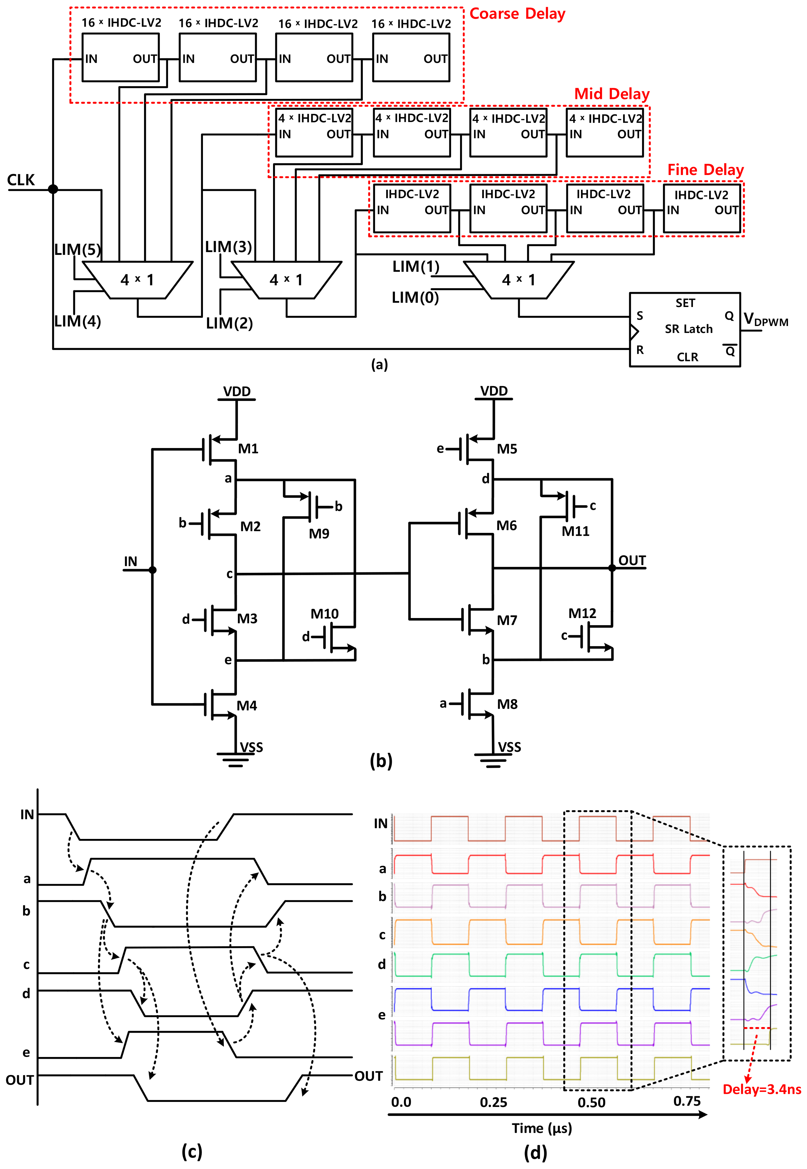
2.2.2. Proposed IHDC-Based DPWM.
The DPWM block is shown in
Figure 6a. The advantages of this architecture are that it does not require any counter and it comprises small-area delay cells. The data that is allowed by the digital limiter is converted to the duty cycle by DPWM. In this architecture, the topology of IHDC greatly reduces the area of DPWM. To avoid loading effect an extra block is used.
In
Figure 6b Interlaced Hysteresis Delay Cell architecture is given. The series M1-M8 plays a key role for delay implementation. The series M9-M12 is responsible for floating node charges/discharges. Node “a” is connected to a, b to b, c to c, d to d and node e is connected to e.
Figure 6c shows the timing diagram of the proposed IHDC, while
Figure 6d shows the simulated delay at each IHDC node. Suppose IN is high which starts to low so M1 is ON and “a” starts to high. When M8 is ON, b starts to low.
When M2 is ON, c starts high which turns on M7 and discharges OUT to ground. To remove the fluctuation in the delay, we can a buffer at output of the delay cell.
In this architecture when the signal changes, there is no short-circuit available. It is because of switching of PMOS and N-type Metal Oxide Semiconductor (NMOS) individually. When the transition is for long duration, the power consumption in the Inverter (INV) is controlled by the short-circuit current. Therefore, the total power is largely reduced compared with the conventional delay cells. Furthermore, there are two paths for current flow; the transistors put the charge in the same path, which results in saving the leakage current. To increase the amount of shared charges and delay, more transistors should be added in a path.
2.2.3. Comparisons of Delay Cells.
Table 1 shows the comparison results of the various delay techniques in a 55-nm CMOS process. In [
23,
24] the INV and AND logic gate take power in the range of 90-to-80 μW. The size is because of 800 transistors. In [
25], the power of the cascaded hysteresis delay cell (CHDC) is 84% less than INV. Similarly, its area is 70% less than INV. The process, voltage and temperature (PVT) variations, however, are two times the conventional delay because of several weakly internal nodes. The application of extra delay cells can overcome delay variation that can increase power and area. Because of PVT, there will be some noise. It can be reduced if the internal nodes of IHDCs are derived perfectly. IHDCs can be used instead of many INV or logic gates to save area and power.
2.2.4. Loop Handover (LHO).
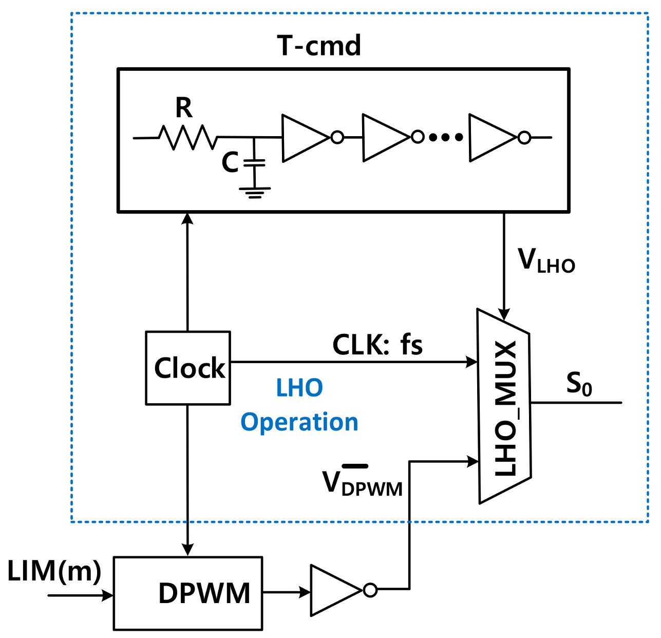
The proposed LHO block diagram shown in
Figure 7. The LHO block was used to solve the problem of the initial transients and to improve the close-loop performance; also, its usage reduced the power consumption, thereby improving the overall efficiency of the converter. The conventional soft-start circuit requires many analog errors, amplifiers, comparators, and capacitor banks. A capacitor bank typically requires the same number of capacitors and bit numbers in the trim-bit control, and this ultimately increases the complexity and the layout area.
However, proposed LHO requires a DPWM with inverter at its output, frequency generation clock and a multiplexer (LHO_MUX). Both the DPWM and the LHO_MUX use the clock simultaneously.
The digital word from the digital limiter is input into the DPWM block to generate the varying duty cycles proportional to the output voltages of the DC-DC converter. During the initial startup, this duty-cycle variation is random and causes instability. To overcome this issue, the DPWM signal is first inverted and masked for a predetermined time, followed by its assignment by the timing-command generator (T-cmd) block. The switching-frequency clock (CLK) source is used in a star manner to reduce the latency. The LHO is accomplished using the inverted DPWM output, T-cmd, and LHO_MUX; the DPWM, T-cmd, and LHO_MUX blocks use the same available CLK. The control-signal VLHO selects the switching source with a 50% duty ratio for 20 us.
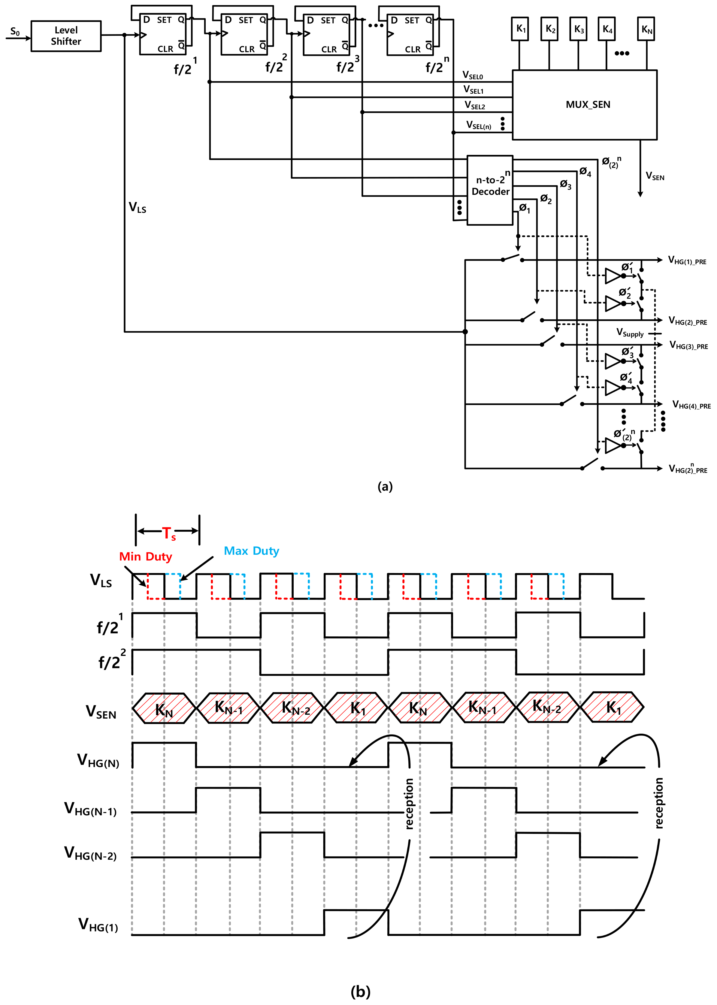
2.2.5. Phase Control.
The phase-control block generates the complementary phases for the gate drivers of the high-side power switches. Onward, the output receives the adjacent signal, at least one output signal is required for the supply voltage.
Figure 8a shows the block diagram of the phase control for N-outputs.
The following two signals can drive the phase-control block: the level shifter signal and the clock divider signal that is used for controlling purpose.
Figure 8b shows a timing diagram of the phase-control logic for N-outputs.
3. Experimental Result
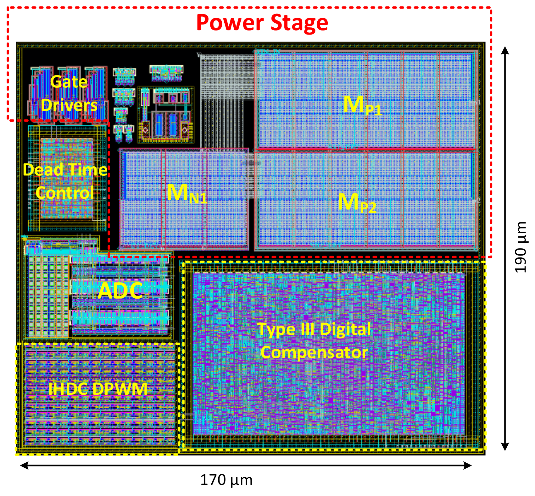
The layout of the proposed SIMO DC-DC converter that is shown in
Figure 9 consists of the proposed digital controller, the DPWM, the digital limiter, gate drivers, the SIMO power stage, and the phase-control blocks. The total active area is 170 × 190 µm.
Figure 10 shows the top simulation result and the measured efficiency with the input voltage of 1.8 V and the output-voltage values of 2.2 and 2.4 V, and the measured efficiency is 94.4%.
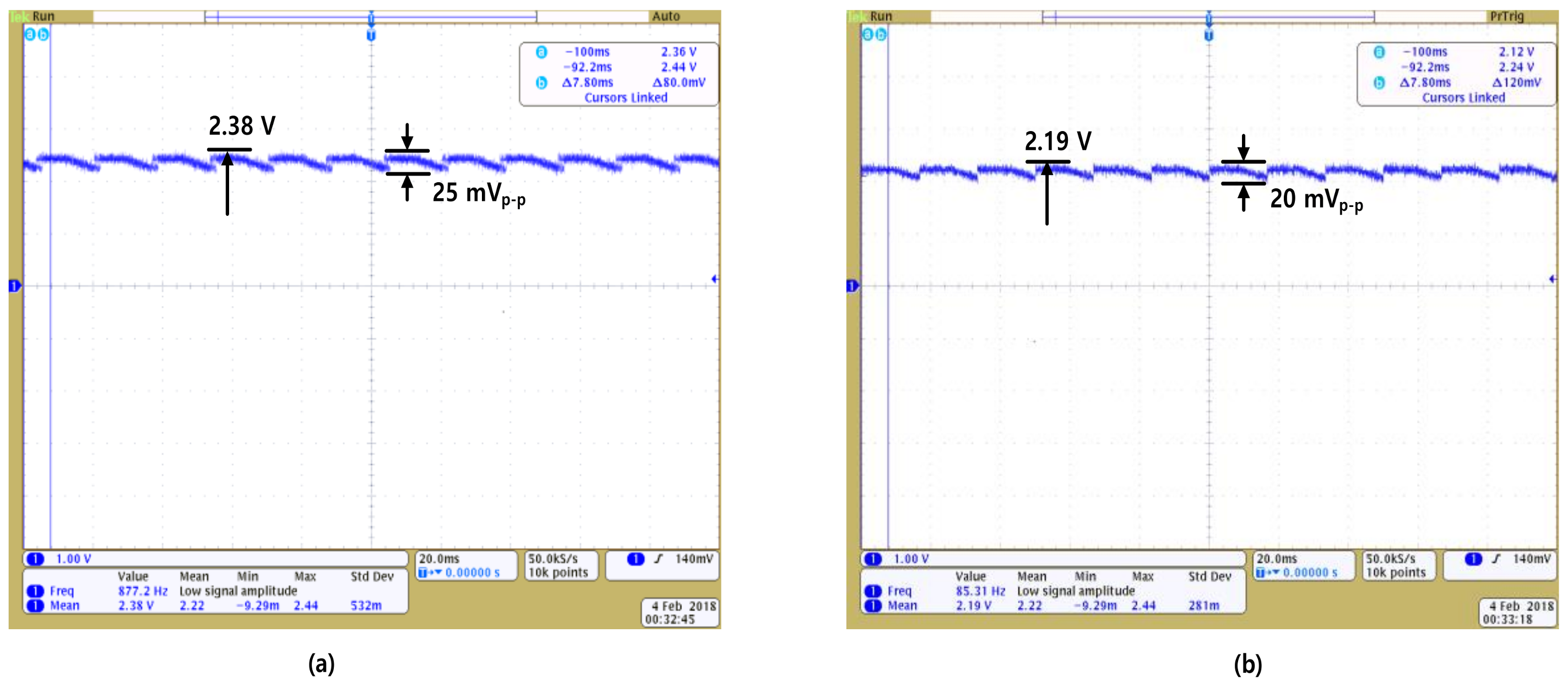
Figure 11a shows the measured output voltage of V
o1. The measured voltage is 2.38 V with the peak-to-peak ripple of 25 mV. The single box resolution of the oscilloscope was set to be 1 V. The decaying voltage was restored by the feedback loop after the sensing by the output sense circuitry, as can be seen in the measurement.
Figure 11b shows the measured output voltage of V
o2, where a constant oscilloscope-measured voltage of 2.19 V is shown. The peak-to-peak ripple for this case was measured to be 20 mV.
Figure 12 shows the load and cross regulations for the V
o1 and V
o2, respectively. The load current was changed from 10 to 80 mA in both cases. The output voltage was reduced by 20 mV for V
o1 at the full load of 80 mA. The output voltage for the V
o2 was reduced by 15 mV at the full load of 80 mA.
Table 2 shows the comparison of this work with the previous works. A very small area of 0.0323 mm
2 and an efficiency of 94.4% are the main differentiate points of this work; compared with the other techniques, this technique required fewer digital-control blocks, and IHDCs which occupy a smaller area and consume less power are used for this architecture. In addition, the compensator of this design is fully integrated, on the other hand, the controllers in the reference works need the FPGA or the cRIO.

 ,
, 


