A DAB Converter with Common-Point-Connected Winding Transformers Suitable for a Single-Phase 5-Level SST System

1
Department of Electrical Engineering, Pusan National University, Busan 46241, Korea
2
Power Conversion and Control Research Center, HVDC Research Division, KERI, Changwon 51543, Korea
*
Author to whom correspondence should be addressed.
Energies 2018, 11(4), 928; https://doi.org/10.3390/en11040928
Submission received: 21 March 2018
/
Revised: 10 April 2018
/
Accepted: 11 April 2018
/
Published: 13 April 2018
(This article belongs to the Special Issue Power Electronics 2018)
Abstract
:One of the main disadvantages of the multi-level solid-state transformer (SST) system is the voltage imbalance on the output of the rectifier modules. This voltage imbalance can be caused by parameter mismatch of the active and passive components, different loads, and the floating structure of the high voltage DC-links. Some studies have been done to solve this voltage imbalance problem. A common way to avoid this imbalance is to balance the voltage of DC-links at the AC/DC conversion stage and balance the power between the modules at the DC/DC conversion stage. Most of these methods require a complex balancing controller or additional circuits. This paper proposes a novel dual active bridge (DAB) converter specialized in power balancing in a single-phase 5-level SST system. The proposed DAB converter does not require any additional balancing controllers or techniques for power balancing. The performance of the proposed DAB converter was verified by simulation and experiments using a 3 kW 5-level SST prototype system.
1. Introduction
Recently, the solid-state transformer (SST) has become an important component of the future power systems because it can replace conventional 50/60 Hz power transformers. Conventional power transformers have a bulky size, a high weight, and power quality issues. Compared to the conventional power transformer, the SST has several advantages in terms of power factor correction, instantaneous voltage regulation, voltage sag tolerance, harmonic isolation, fault management, and bidirectional power control. In addition, the SST can reduce the volume and weight dramatically by increasing the operation frequency [1,2,3,4,5,6]. Because of these advantages, the SST is used in isolated battery chargers, in the field of aviation, in ships, and as renewable energy sources [7].
Various SST topologies for single-phase applications have been reported and discussed in [8]. A multi-stage power converter is the basic configuration that is typically used to achieve the SST system [2,4,9]. This system consists of an AC/DC conversion stage, a DC/DC conversion stage with high-frequency isolation, and a DC/AC conversion stage [10]. In this paper, a cascaded H-bridge (CHB) rectifier was adopted for the AC/DC conversion stage. This CHB enables the modular design of the power stage. The dual active bridge (DAB) converter, which is mostly preferred for high-power applications, is adopted for the DC/DC conversion stage [11,12]. The DC/AC conversion stage was omitted because it is beyond the scope of this paper.
One of the main disadvantages of the multi-level SST is the voltage imbalance on the output of different rectifier modules [13,14]. This unbalanced DC-link voltage can be caused by unbalanced load condition, mismatch of the active and passive components, and the floating structure of the high voltage DC-links [15,16,17]. Because of this unbalanced DC-link voltage and power, there is an increase in the stress of the semiconductor device, and there are over-voltage or over-current problems that can lead to the collapse of the entire system.
Many methods have been proposed to solve the imbalance of DC-links. A common way to avoid this imbalance is to adjust the real power of each H-bridge [18,19,20,21]. However, the adjustable real power range of each H-bridge is limited by the input AC voltage and the voltage reference of DC-links. Therefore, an additional power balance control is needed to overcome these constraints.
This paper proposes a novel DAB converter specialized for power balancing in the single-phase 5-level SST system. This DAB converter has a common-point-connected winding transformers on its secondary side. This common point connected transformers are formed by arranging each end of the coils so that they are connected at a common point. This is the same as removing one transformer from a three-phase wye-connected transformer. There are several topologies using three-phase wye-connected transformers [22,23,24,25]. However, they are not focused on the balance of the DC-links and are unsuitable for the single-phase SST system. The proposed DAB converter, suitable for the single-phase 5-level SST system, can balance the power between DC-links without additional circuits, controls, or special pulse width modulation (PWM) schemes.
The rest of this paper is organized as follows: The conventional power balancing methods of the DAB converter are introduced in Section 2. The proposed topology is analyzed theoretically in Section 3. In Section 4, the simulation results are presented to verify the effectiveness of the proposed topology. The experimental results using a 3 kW 5-level SST prototype system are presented in Section 5. Finally, the conclusion is presented in Section 6.
2. Conventional Power Balancing Methods of the Dual Active Bridge Converter
The DAB converter has been widely used because of various advantages such as high power density, bi-directional power flow, galvanic isolation, and so on [11,26]. Most DAB converters consist of half-bridge or full-bridge circuits, which produce 2-level square waves across the high-frequency transformer as shown in Figure 1. Conceptually, the DAB converter can be viewed as an interfacing inductor driven at either end by a controlled square-wave voltage source. The interfacing inductance is the sum of the transformer leakage inductance and the external inductance. The external inductor is needed in order to adjust the output power as well as to extend the zero voltage switching operation [27]. The amount of power transferred by the DAB converter is determined by the interfacing inductance and the phase difference between active bridges. Therefore, the tolerance of the magnetic elements causes power and voltage imbalance of the DC-links in the SST system.
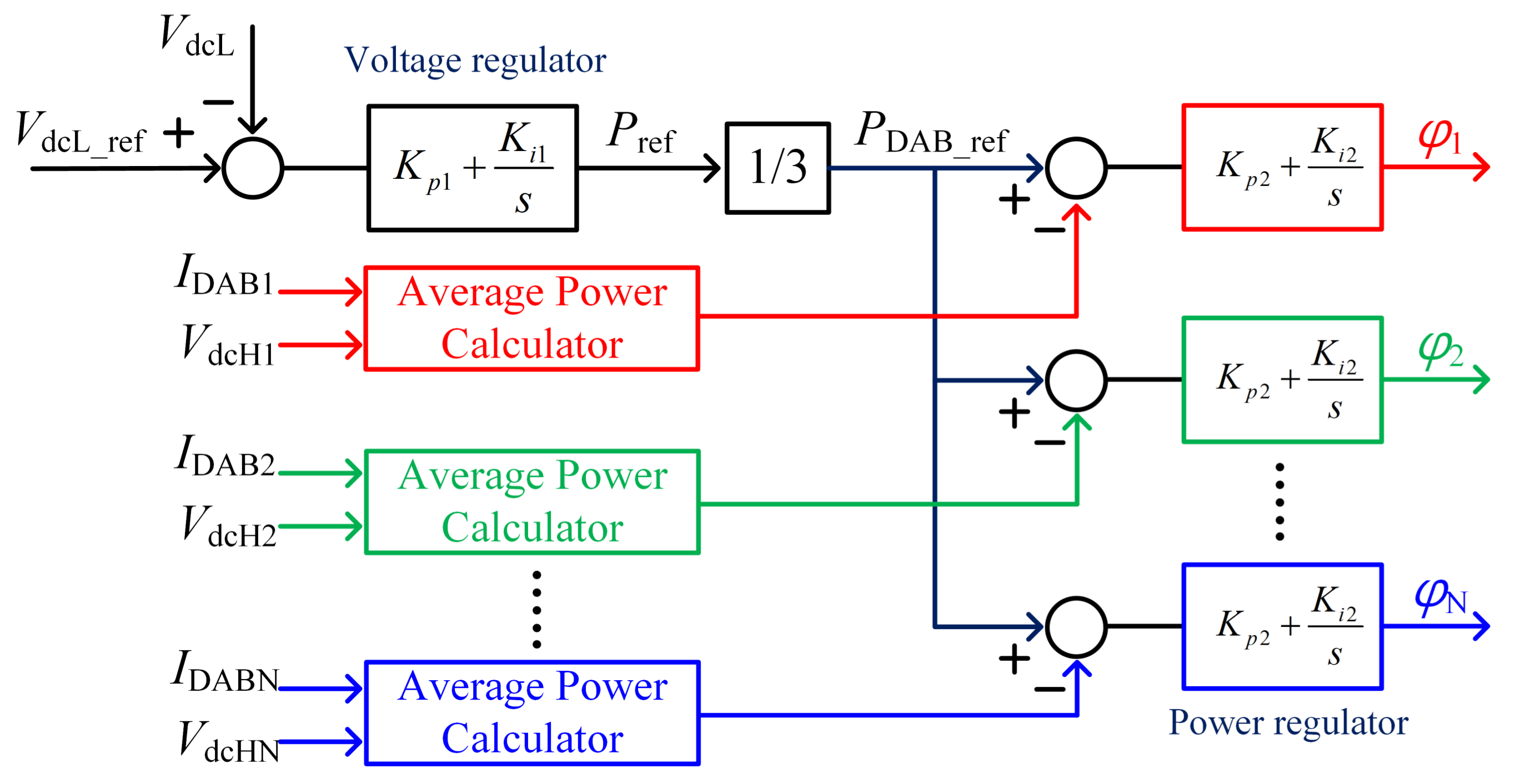
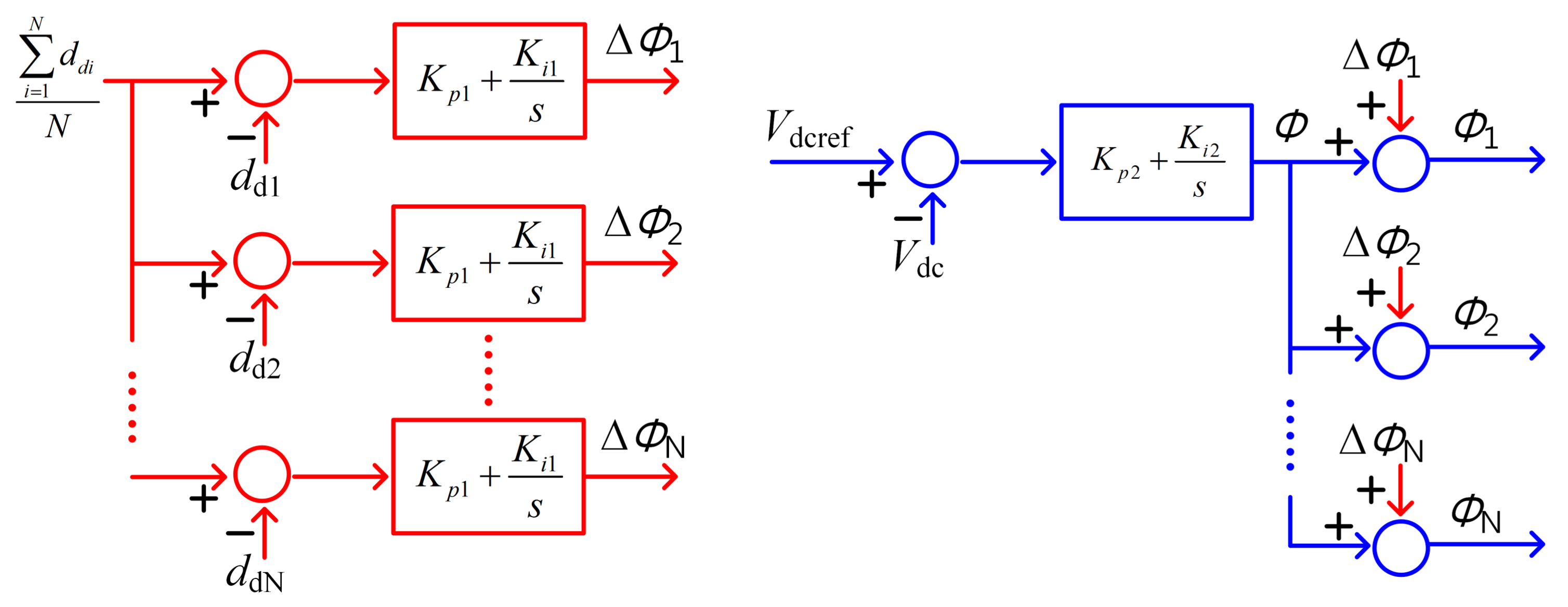
Many methods have been studied to prevent the power imbalance of DC-links in the SST system. A power balancing controller has been proposed in [28], which is depicted in Figure 2. The average power of the DAB converter is calculated, and a different phase shift is generated for each of them. This method needs additional current sensors for the DAB stage, which increases system costs. In addition, the calculation of the power is also not easy due to the complex integration operation, in which the calculation accuracy may be low. Another power balancing controller has been proposed in [29], which is depicted in Figure 3. This method uses the active power component of the duty cycle in the rectifier stage as the feedback signal for the power balancing controller. This power balancing controller does not need any current sensor for the DC/DC stage, but still requires a complex balancing controller. In addition, several power balancing methods based on complex controllers, additional circuits, or special PWM schemes have been studied [30,31,32].
However, unlike conventional power balancing methods, the proposed DAB converter can balance the power between DC-links without additional circuits, controls, or special PWM schemes.
3. Theoretical Analysis of the Proposed DAB Converter
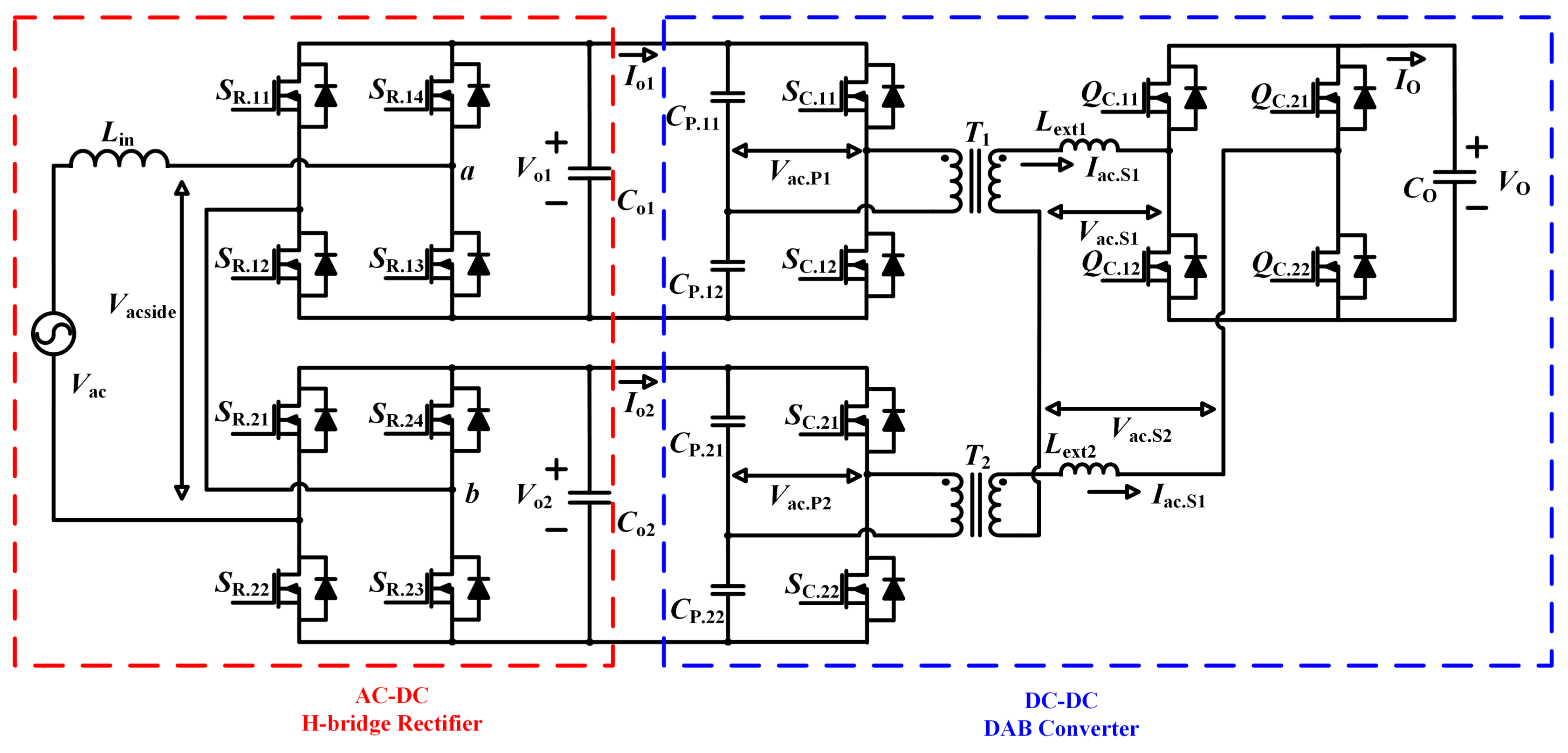
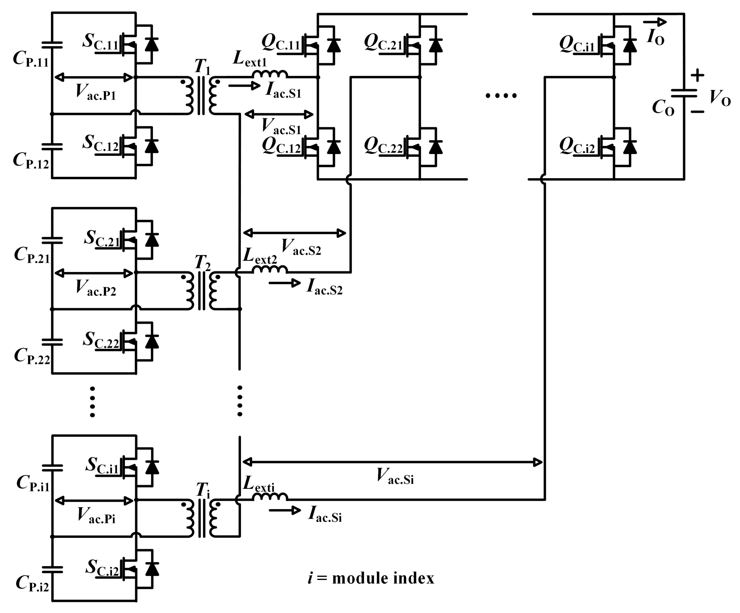
Figure 4 presents the entire system configuration of the single-phase 5-level SST system. As mentioned in Section 1, the AC/DC conversion stage of the SST system employs CHB rectifier modules. The role of this rectifier module is to control the input power factor, rectify the input AC voltage to DC-links, and balance the voltage of DC-links. In this paper, the phase shift pulse width modulation (PSPWM) scheme was adopted for CHB rectifier modules because it is easy to use and reliable [33,34]. The single phase d-q coordinate controller was also adopted for voltage balancing of the DC-link as presented in [35]. The detailed PWM scheme, control, and analysis of the CHB rectifier were omitted because it is beyond the scope of this paper.
3.1. Operation of the Proposed DAB Converter
Several assumptions were made before analysis. First, all active devices are lossless and linear components. Second, the voltage of the capacitors named (, i,j = 1, 2) and is constant within the switching period. This can be achieved when their capacitances are large enough. Third, to simplify the discussion, the different voltage levels of each bridge are matched by choosing an appropriate number of turns for winding ( = ). The turn ratio of each transformer is identical.
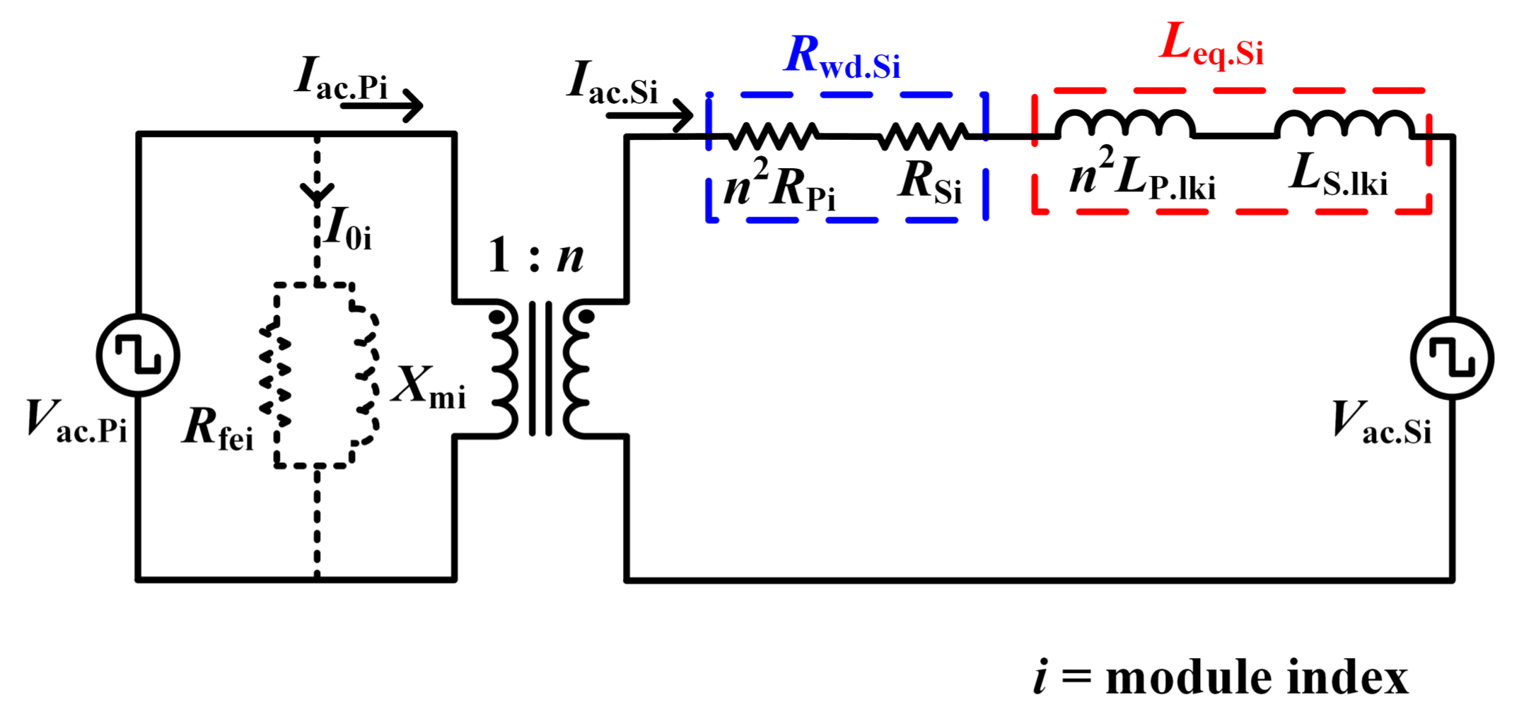
The structure of the proposed DAB converter is divided into three parts. The primary side consists of two separate half-bridge circuits which are connected to the individual DC-links. Two transformers with a pair of secondary windings are connected to each other. Secondary legs of each module are configured in the form of a full-bridge circuit. Figure 5 shows a transformer equivalent model with equivalent impedance referred to the secondary side. In Figure 5, i is the module index, is the square-wave voltage at its primary bridge, is the square-wave voltage at its secondary bridge, and are primary and secondary currents of transformer, is the primary winding resistance, is the secondary winding resistance, n is the turn ratio, is the primary side leakage inductance, is the secondary side leakage inductance, is the iron loss resistance of the transformer, is the magnetizing inductance seen from the primary winding, is the excitation current, is the equivalent winding resistance referred to the secondary side, and is the leakage inductance referred to the secondary side. To simplify the discussion, is neglected because it is too small compared with the total current of the transformer. However, in the simulation section, the function of auto-balancing was verified with different values.
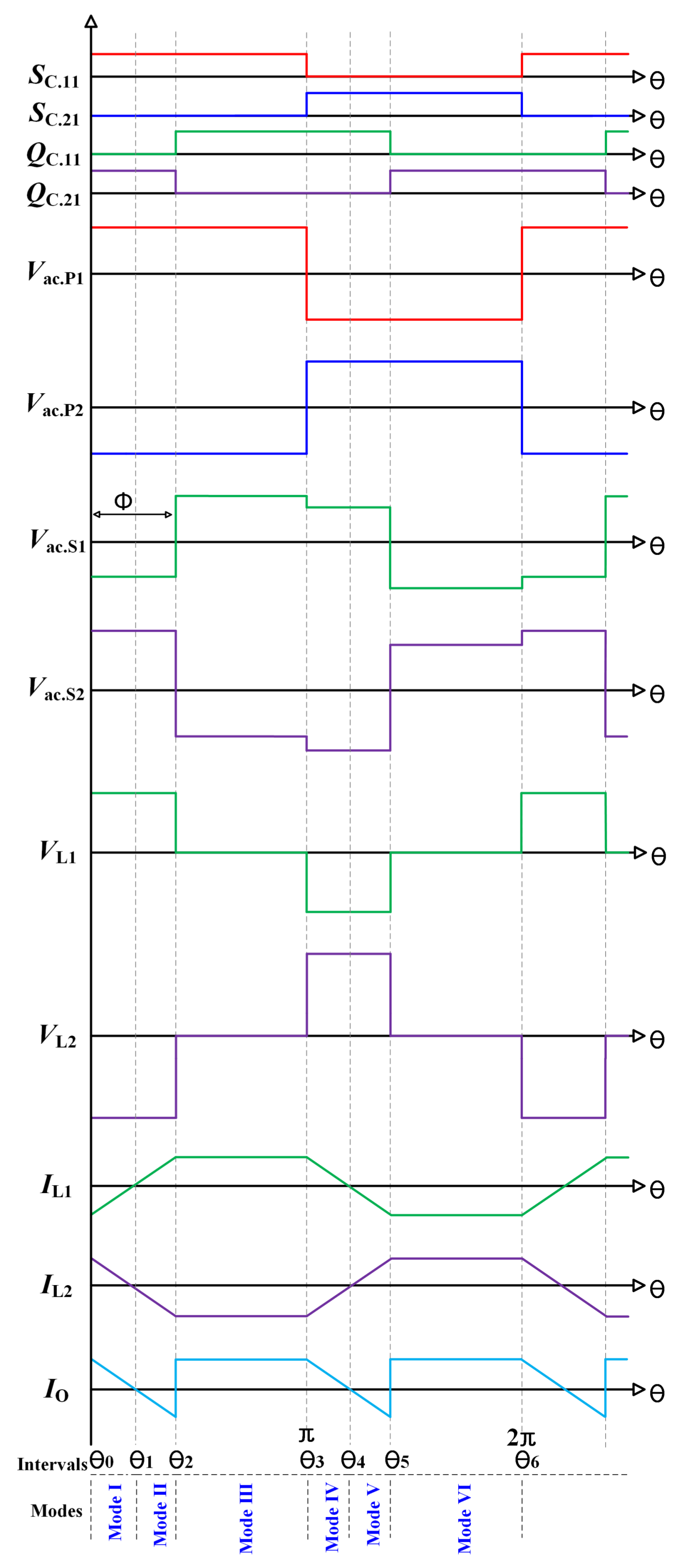
The switching scheme for the proposed DAB converter is based on the interleaved single phase shift (SPS) modulation. The modulation of SPS has one degree of freedom , which is the phase difference between square-wave voltage of the primary and secondary bridges [12,36]. The amount of power transferred by the DAB converter is determined by the . All legs, consisting of two complementary switches, are operated with a 50% duty cycle to transfer the maximum power. For interleaved operation, the square-wave voltage of each primary bridge denoted as and are phase-shifted with respect to each other by T/2, where T is the switching period. In the same manner, the square-wave voltage of each secondary bridge, denoted as and , are phase-shifted with respect to each other by T/2. In addition, in order to simultaneously turn on/off the diagonal opposite switches in the secondary full-bridge circuit, the phase difference between each module should be identical.
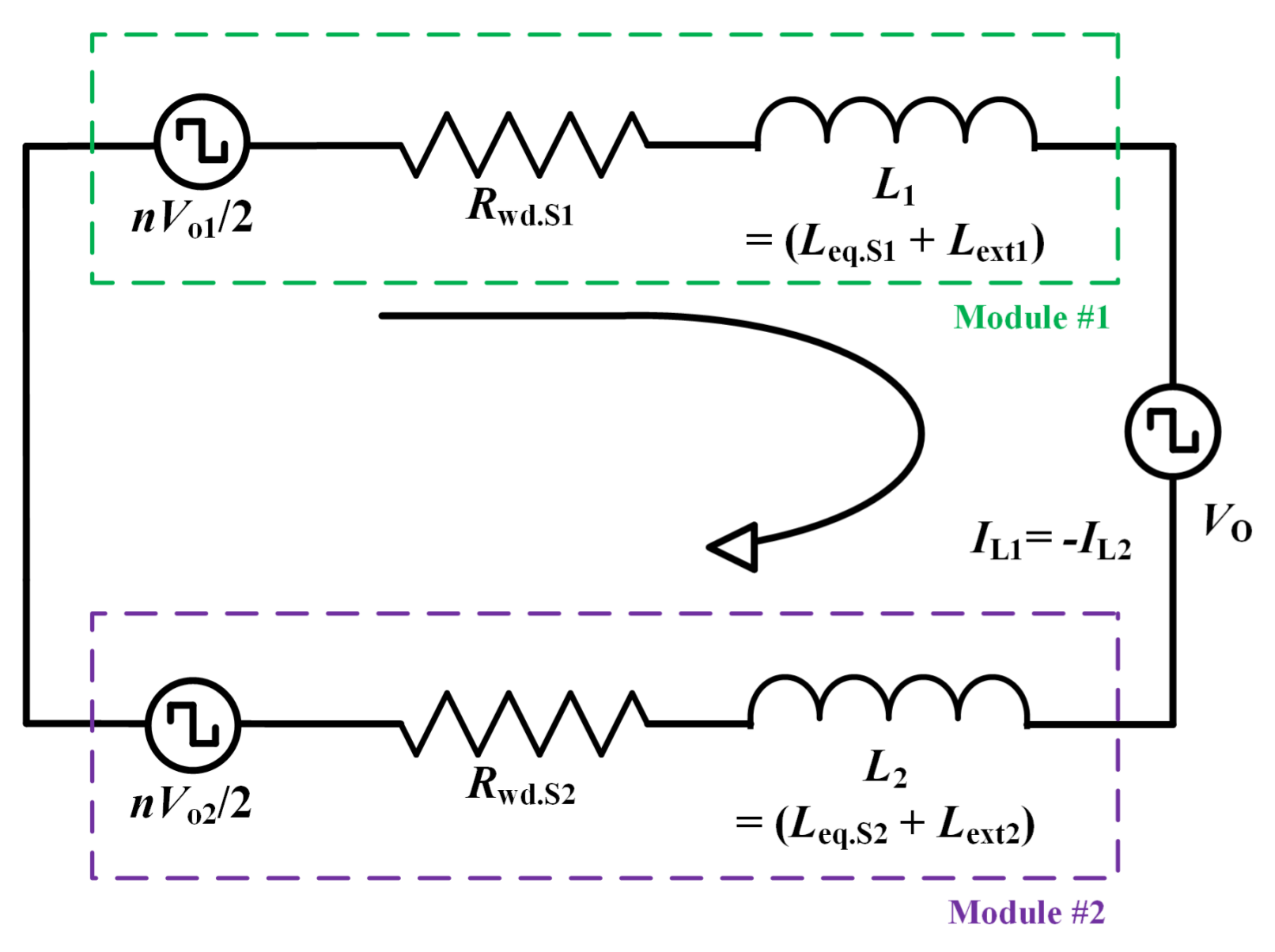
According to the above described switching scheme and Figure 5, the proposed DAB converter can be represented by an equivalent circuit, as shown in Figure 6, where (, i = 1, 2) and are the input and output DC voltages, (, i = 1, 2) represents the external secondary inductance, which is needed in order to adjust the output power as well as to extend the zero voltage switching operation [27], and (, i = 1, 2) is the interfacing inductance, which is the sum of the (, i = 1, 2) and the (, i = 1, 2). The voltage applied across each interfacing inductor can be represented by the following equations.
where is the electrical angle in radians.
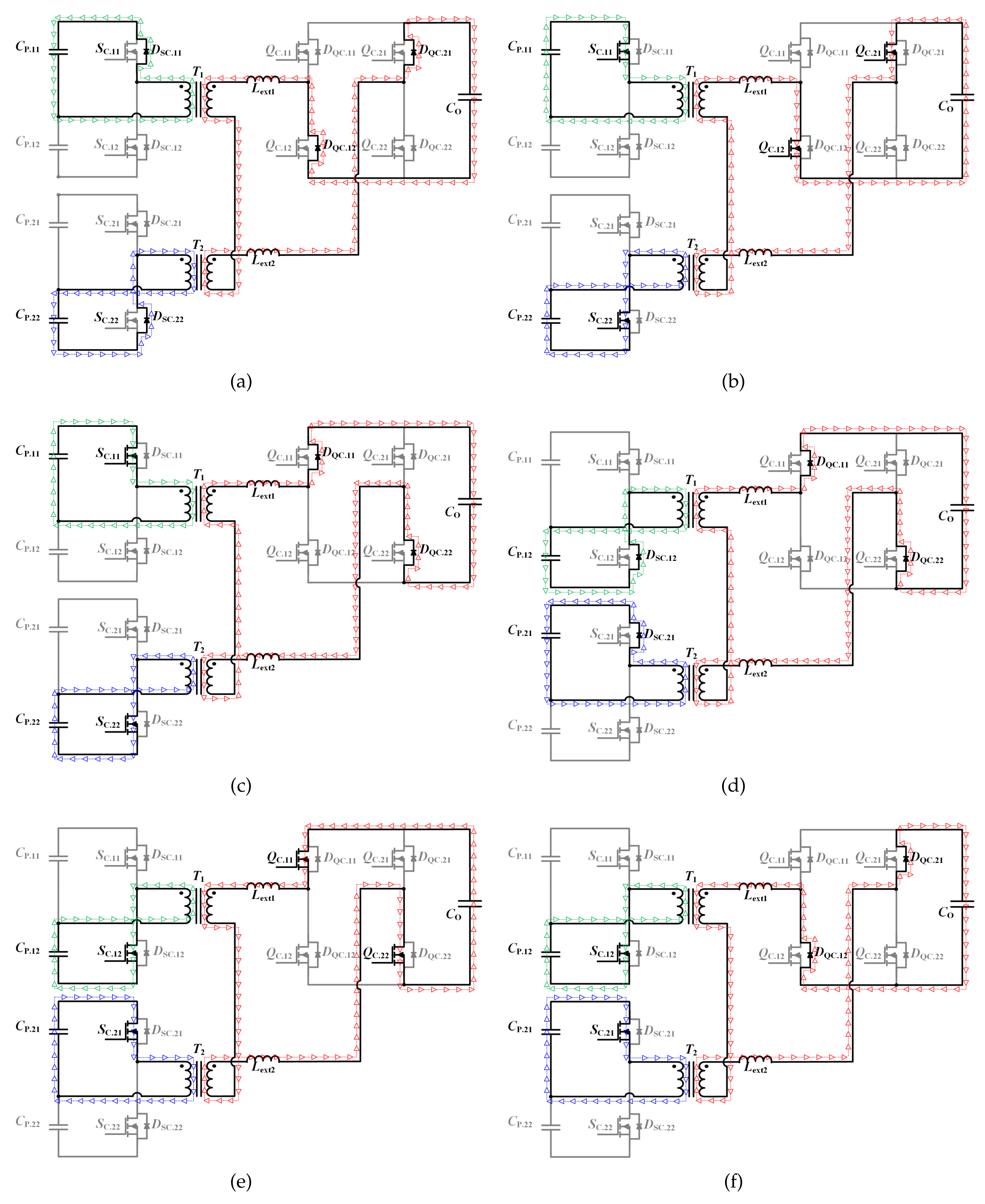
The proposed DAB topology has six operation modes over one switching cycle. Figure 7 and Figure 8 show the operating modes and the corresponding waveforms, respectively.
Mode I [ to ] (Figure 7a): The negative to positive transition of is triggered by turning off . At the same time, is triggered from positive to negative by turning off . In the beginning of this mode, the current flows naturally through anti-parallel diodes , , , and . Switches , , , and are then turned on by zero voltage switching (ZVS). During this mode, (, i = 1, 2) represents induced constant DC-link voltage of and , respectively. The voltage across the inductors, and , are given by Equations (1) and (3), respectively. The current on the upper inductor flows in the negative direction. On the other hand, the current on the lower inductor flows in the positive direction. The current of the output capacitor, , flows in the direction of charging the output capacitor, . The slope of is negative. This mode ends when reaches zero.
Mode II [ to ] (Figure 7b): During this mode, the current flows through , , , and . and are the same as Mode I. flows in the positive direction. In contrast, flows in the negative direction. flows in the direction of discharging . The slope of is still negative.
Mode III [ to ] (Figure 7c): During this mode, and are given by Equations (2) and (4), respectively. Current flows through , , , and . flows in the direction of charging . The slope of is changed to zero.
Mode IV [ to ] (Figure 7d): The positive to negative transition of is triggered by turning off . At the same time, is triggered from negative to positive by turning off . In the beginning of this mode, the current flows naturally through the anti-parallel diodes , , , and . Switches , , , and are then turned on by ZVS. During this mode, (, i = 1, 2) represents induced constant voltage of and , respectively. and have the same magnitude and opposite sign compared to Mode I. flows in the positive direction. On the other hand, flows in the negative direction. flows in the direction of charging . The slope of changes to negative. This mode ends when reaches zero.
Mode V [ to ] (Figure 7e): During this mode, the current flows through , , , and . and are the same as Mode IV. flows in the negative direction. On the other hand, flows in the positive direction. flows in the direction of discharging . The slope of is still negative.
Mode VI [ to ] (Figure 7f): During this mode, and are the same magnitude with an opposite sign compared to Mode III. The current flows through , , , and . flows in the direction of charging . The slope of is zero.
3.2. Analysis of the Power Balancing Function
According to Equations (1) to (4), and Figure 8, the average current flowing through the DC-links, denoted as and , can be calculated as follows:
where is the switching angular frequency of the proposed DAB converter.
and are always identical despite non-identical parameters such as winding resistance, leakage inductance, and external inductance. This characteristic is distinguished from other parallel-output DAB converters. In other parallel-output DAB converters, the tolerance of the magnetic elements cause non-identical average current flowing through the DC-links and additional balancing techniques are used to compensate for this imbalance. However, the proposed DAB converter can maintain the identical current without additional circuit, control or a complex switching scheme despite of non-identical magnetic elements. This is because two common point connected transformers and a secondary full-bridge circuit form a single close loop by interleaved SPS modulation. The current flowing through the single close loop is always identical ( = ). The current referred to the primary side of the transformer is also identical ( = ). This is the physical reason that and are always identical. In summary, the proposed DAB converter can be represented to identical current sources connected to each DC-link, so that the amount of power transferred from the DC-link are always identical if the CHB rectifiers balance the voltage of the DC-links.
3.3. Limitations of Module Expansion
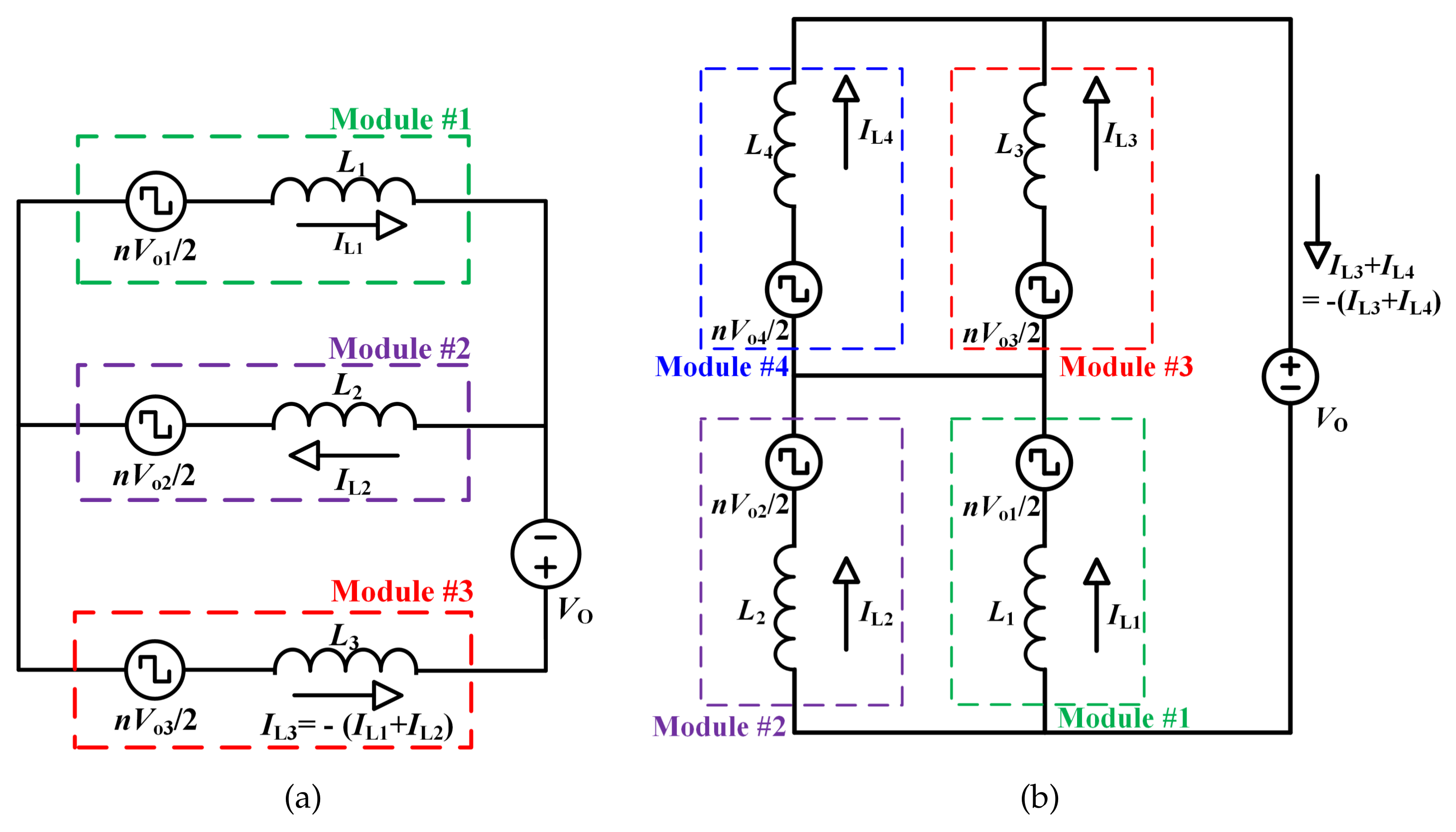
This section discusses the limitations of module expansion using the proposed DAB converter. To simplify the discussion, ideal transformers are applied to the analysis. When the seven or more levels of the SST system are configured, it is assumed that the proposed DAB converter is expanded as shown in Figure 9. Figure 10a,b show the equivalent circuits when the number of modules is expanded to three and four, respectively. Unlike when the number of modules is two, the equivalent circuits of the expanded module does not form a single close loop. This means that the current flowing through each primary circuit can vary due to the difference in inductances.
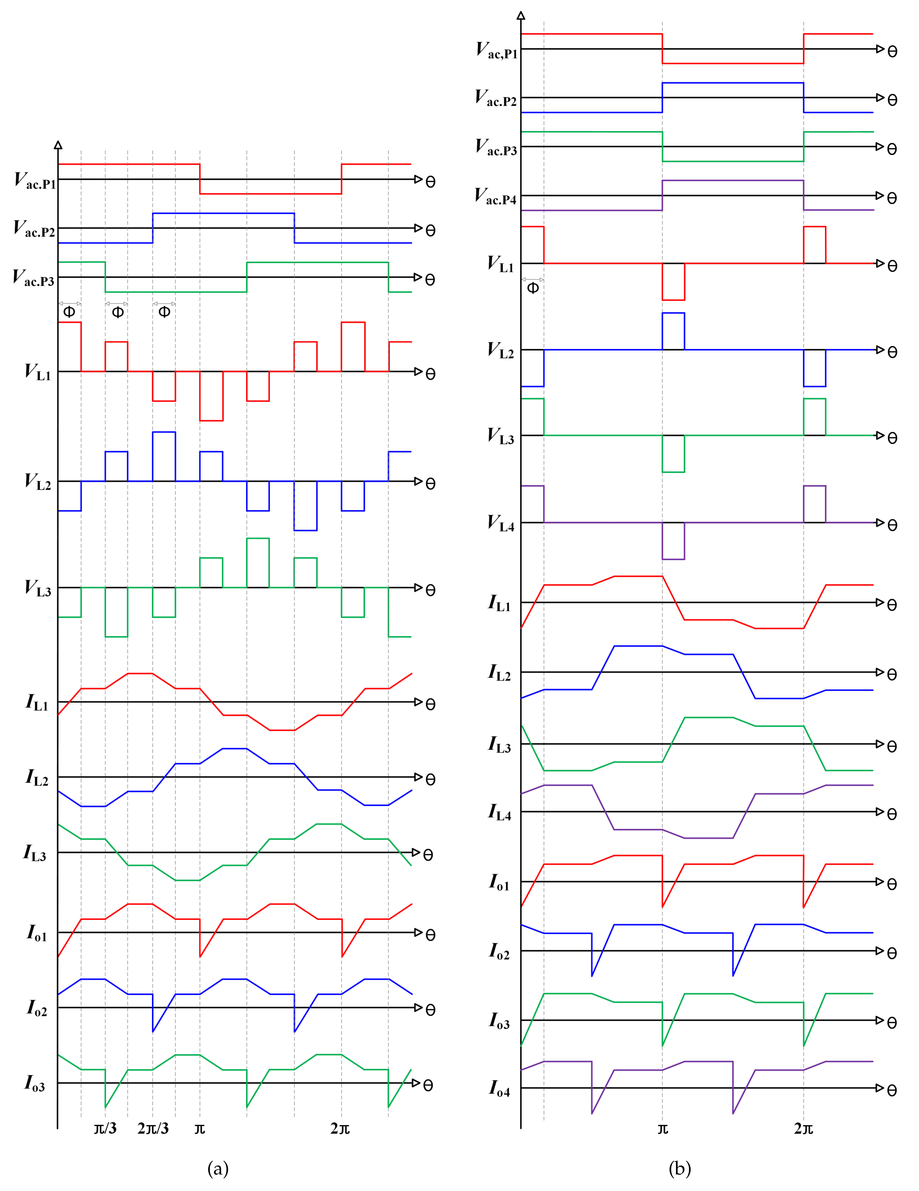
Figure 11a,b show the theoretical waveforms when the number of modules is expanded to three and four, respectively. In Figure 11, (, i = 1∼4) represents the square-wave voltage of its primary bridges, (, i = 1∼4) represents the voltage of the external inductors, (, i = 1∼4) represents the current flowing through the external inductors, and (, i = 1∼4) represents the current flowing through the individual DC-links.
When the number of modules is three, the average current flowing through the DC-links can be obtained by referring to Figure 11a.
When the number of modules is four, the average current flowing through the DC-links can be obtained by referring to Figure 11b.
Referring to the above equations, it can be seen that the average current flowing through the DC-links can vary depending on the difference in inductances as expected. If the current imbalance exceeds the balancing capability of the rectifier, the voltage of DC-links becomes unbalanced. Therefore, additional balancing techniques are required for three or four expanded modules.
4. Simulation Result
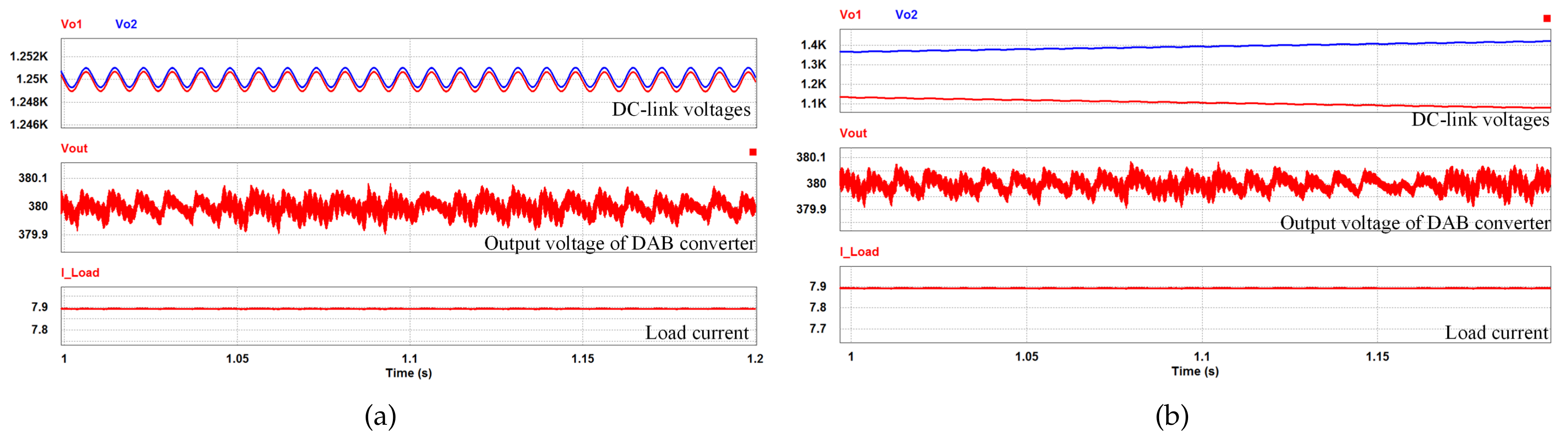
The 5-level SST system is simulated here for a 3 kW rated power transfer with 2.2 k for the input and 380 for the output. The system parameters were designed according to Table A1. To verify the power balancing capability of the proposed DAB converter, the simulations were performed using magnetic elements with tolerance. The CHB rectifiers do not balance the voltage of DC-links. In this case, if the average current flowing through the DC-links is non-identical, a voltage imbalance of DC-links will occur. Figure 12a,b present the simulation results using a common-point-connected winding transformer on its secondary side or not, respectively. A comparison of the two cases showed that the proposed DAB converter, which uses common-point-connected winding transformers on its secondary side, have balanced DC-link voltages (, ) of 1.25 k even though the inductances are different.
Figure 13a,b show the waveforms when the number of modules is expanded to three and four with common-point-connected winding transformers, respectively. In both cases, has 150 H and the others have 110 H. Ideal transformers are used as analyzed in the previous section. The voltage of the DC-links diverges, unlike the case where the number of modules is two. All simulation results demonstrate the feasibility of the aforementioned analysis (in Section 3).
5. Experimental Result
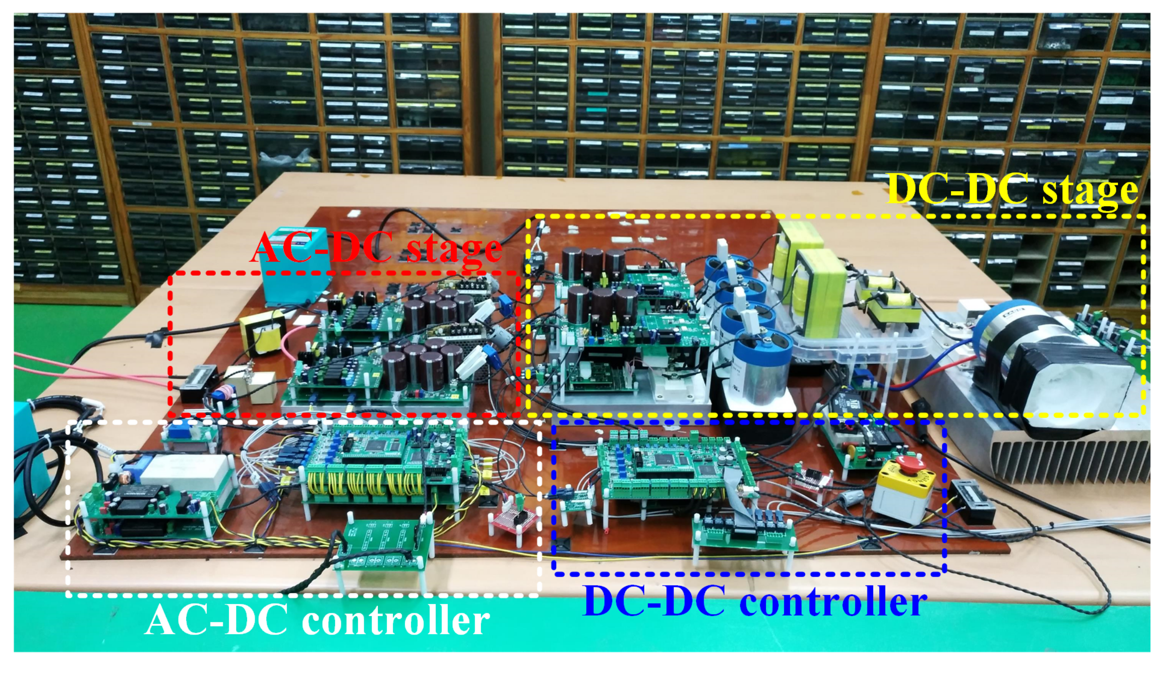
Figure 14 shows the 5-level SST prototype system that employs the proposed DAB converter. A step-up transformer (380 V/2200 V) is connected to CHB rectifier modules to supply high-input AC voltage. The rectifier stage consists of two CHB rectifier modules that control the input power factor, rectify the input AC voltage to DC-links (2500 ), and balance the voltage of the DC-links. The DC/DC conversion stage consists of the proposed DAB converter modules that employ common-point-connected winding transformers on its secondary side. The proposed DAB converters are connected to each DC-link to regulate a common low DC output voltage on the system output stage (380 ). The traditional 50/60 Hz power transformer is replaced with high-frequency transformers in the DAB modules and solid-state devices, which are the key point in achieving reductions in both size and weight. The entire operation of the SST system was programmed by DSP and CPLD processors. The AC/DC conversion stage and the DC/DC conversion stage have their own DSP controllers. The system parameters were designed according to Table A1 (See Appendix A).
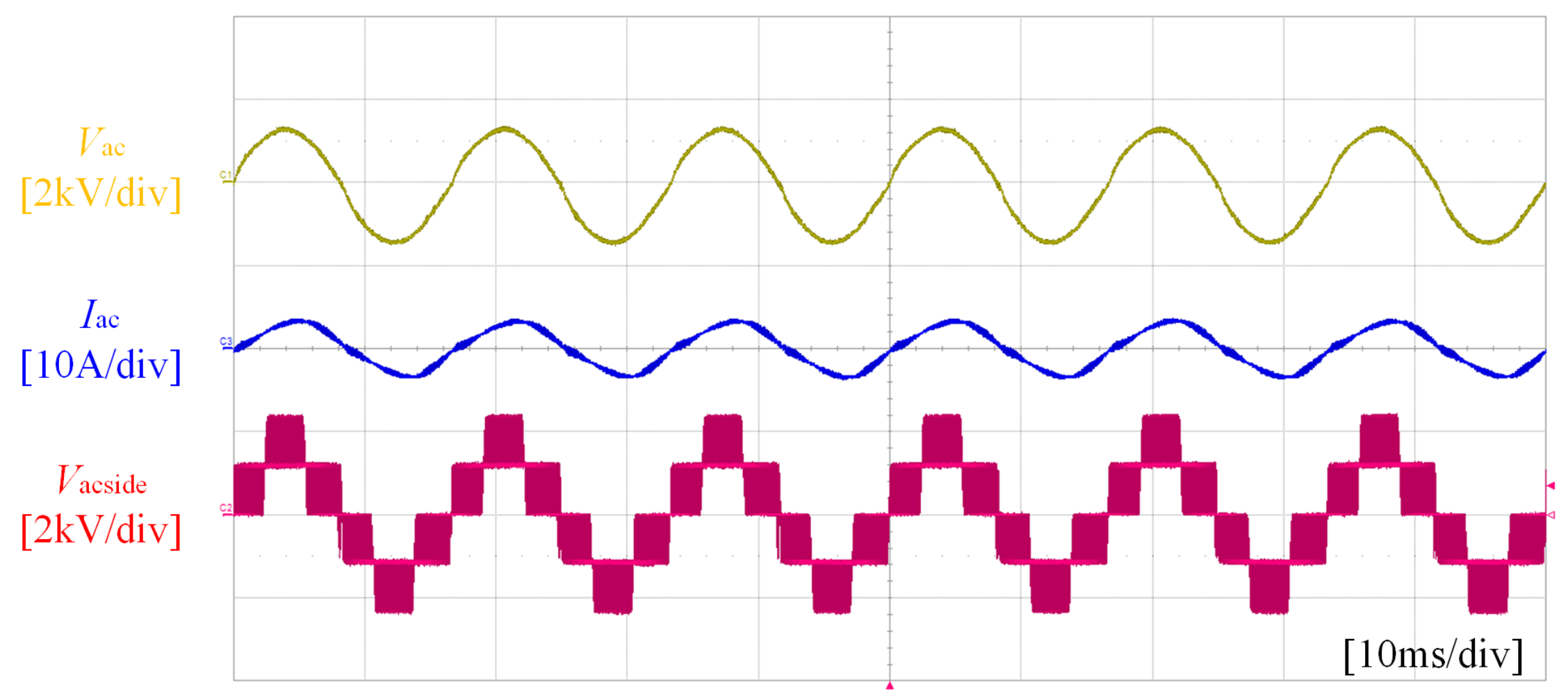
Figure 15 shows the experimental waveforms of the 5-level CHB rectifier modules that control the input power factor and rectify the input AC voltage to DC-links (2500 ). The 5-level CHB rectifier modules are normally operating under a rated 3 kW load condition.
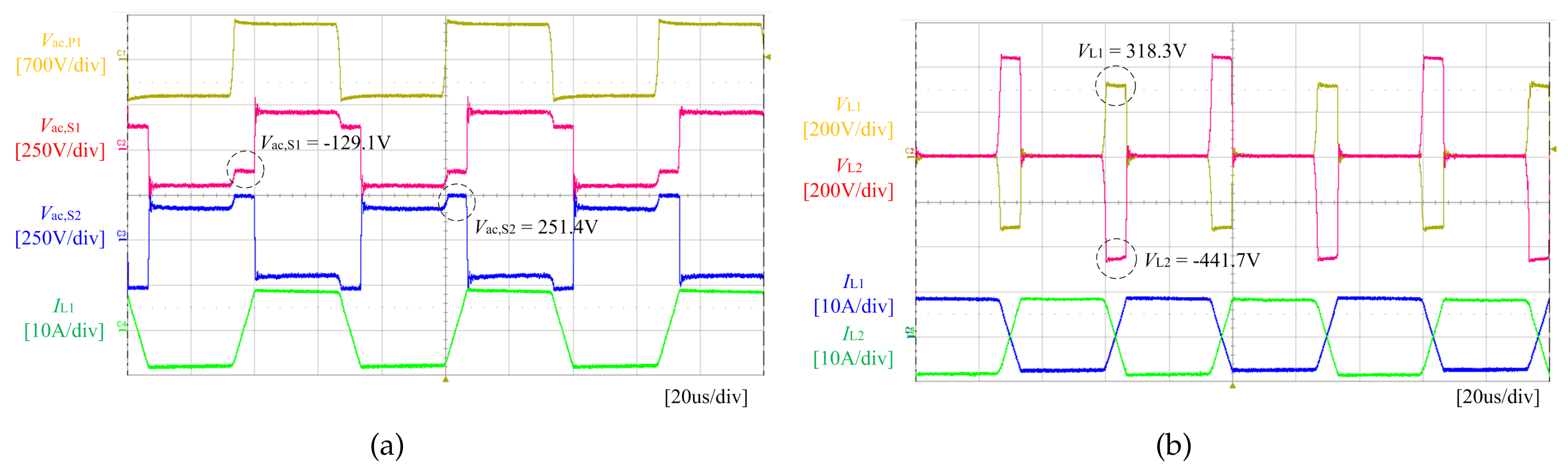
Figure 16a shows the interfacing inductor current () and the voltages on the primary and secondary bridges (, , and ). According to the analysis in Section 3, the voltage on the secondary bridges ( and ) can be calculated during the intervals to to −128.7 V and 251.3 V, respectively. The measured values experimentally are −129.1 V and 251.4 V, respectively. Figure 16b shows the voltage and current waveforms of the inductors (, , , and ). In the same manner, the voltage across inductors ( and ) can be calculated during intervals to to 318.7 V and −441.3 V, respectively. The experimentally measured values are 318.3 V and −441.7 V, respectively. The calculated values are almost the same as the measured values. Therefore, the aforementioned analysis in Section 3 is reliable.
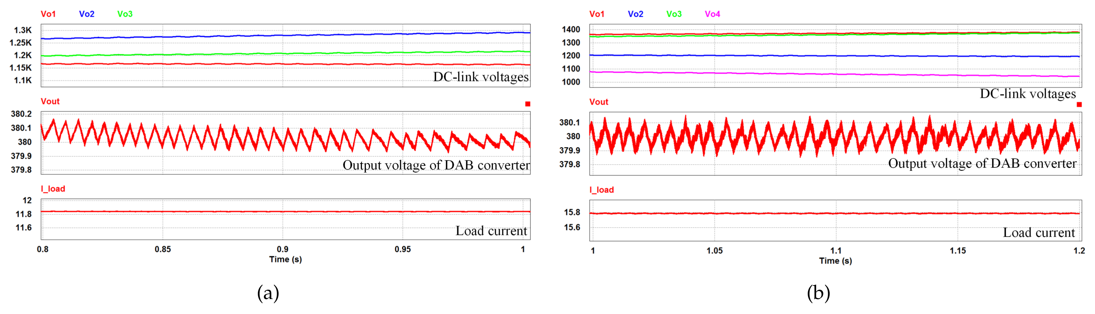
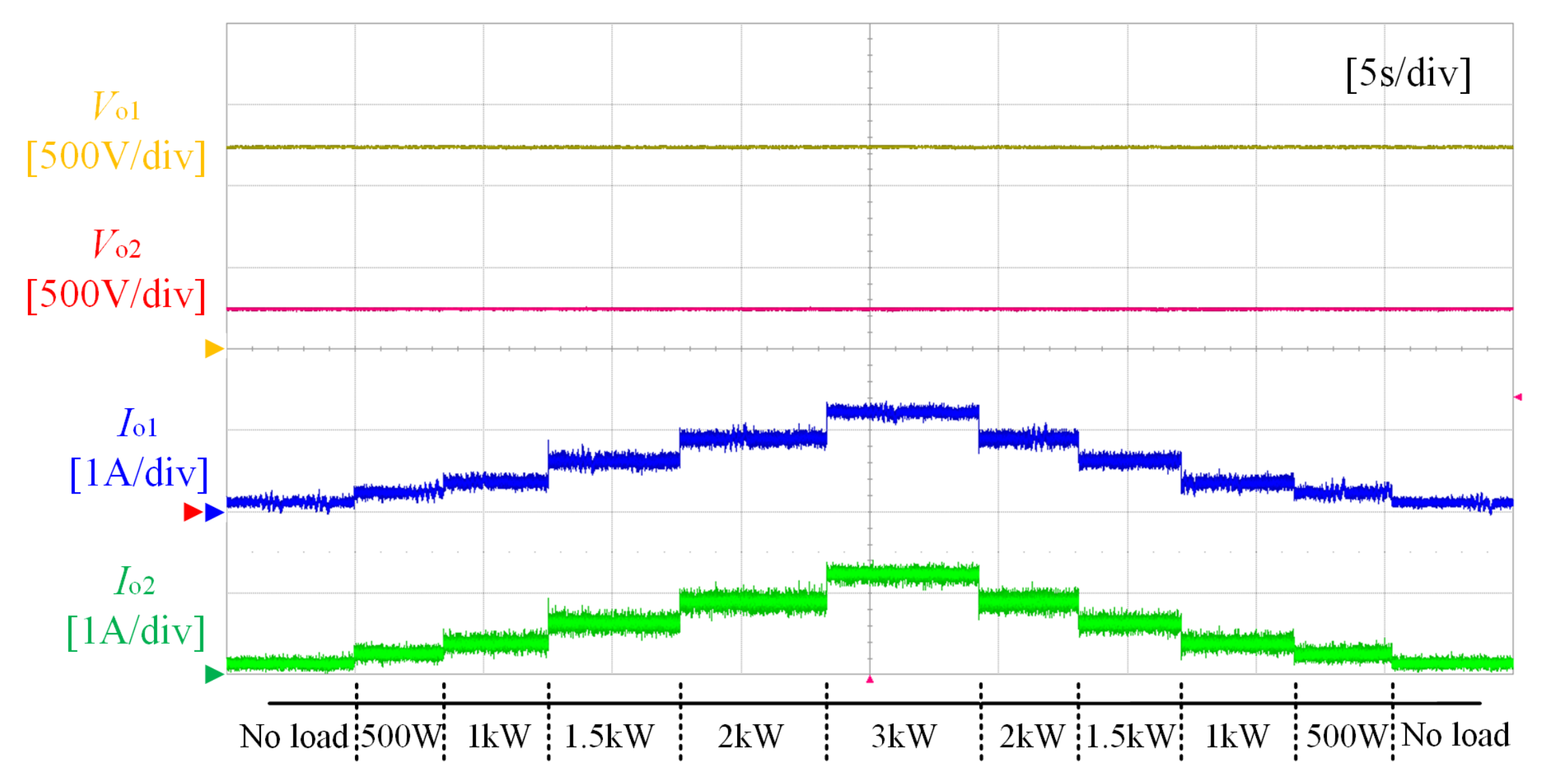
Figure 17 shows the experimental waveform of the balanced DC-links under various step load changes. The voltage and current of each DC-links is well balanced when the load is changed randomly to 3 kW.
6. Conclusions
In this paper, a novel DAB converter specialized in power balancing in a single-phase 5-level SST system was proposed. The structure of the proposed DAB converter is divided into three parts. The primary side consists of two separate half-bridge circuits that are connected to individual DC-links. Two transformers with a pair of secondary windings are connected to each other. Secondary legs of each module are configured in the form of a full-bridge circuit. When this novel DAB converter is driven by the interleaved SPS modulation, the average current flowing through the DC-links in the 5-level SST is always identical. Therefore, the proposed DAB converter does not require any additional balancing controller or techniques, which is essential to power balancing in conventional methods. Theoretical analysis and formulas for all of these processes are provided in detail.
A 3 kW single-phase 5-level SST experimental prototype system was constructed to validate the power balancing capability of the proposed DAB converter. The theoretical analysis, calculations, and experimental results demonstrate that the proposed DAB topology has a good power balancing capability.
Based on the results of this paper, a novel DAB converter specialized in power balancing in an SST system with seven or more levels will be studied will be studied in the future.
Acknowledgments
This research was supported by the KERI Primary research program of MSIP/NST (No. 18-12-N0101-04).
Author Contributions
All the authors gave equal contributions in writing and revising the paper.
Conflicts of Interest
The authors declare no conflict of interest.
Appendix A. System Parameters

Table A1.
System parameters.
| Parameter | Symbol | Value | Unit |
|---|---|---|---|
| Rated output power | 3 | kW | |
| Input AC voltage | 2.2 | kV | |
| Peak input AC voltage | 3.1 | kV | |
| Each DC-link voltage | , i = 1, 2 | 1.25 | kV |
| Total DC-link voltage | 2.5 | kV | |
| Capacitance of DC-links | , i = 1, 2 | 500 | F |
| Line inductance | 5 | mH | |
| Switching frequency for rectifier | 10.8 | kHz | |
| Switching frequency for converter | 15 | kHz | |
| Primary half bridge capacitor | , i,j = 1, 2 | 100 | F |
| Output voltage of DAB converter | 380 | V | |
| Capacitance of output voltage | 1 | mH | |
| Transformer turn ratio | n | 1:0.302 | |
| Primary turns of DAB | 43 | ||
| Secondary turns of DAB | 13 | ||
| Secondary upper inductor | 150 | uH | |
| Secondary lower inductor | 110 | uH | |
| Magnetizing inductance of | 10 | mH | |
| Magnetizing inductance of * | 5.5 | mH | |
| Iron loss of * | 15.6 | kohm | |
| Iron loss of * | 8.6 | kohm | |
| Primary winding resistance of * | 100 | mohm | |
| Primary winding resistance of * | 55 | mohm | |
| Secondary winding resistance of * | 12 | mohm | |
| Secondary winding resistance of * | 6.6 | mohm |
* simulation only.
References
- Kang, M.; Enjeti, P.; Pitel, I. Analysis and design of electronic transformers for electric power distribution system. IEEE Trans. Power Electron. 1999, 14, 1133–1141. [Google Scholar] [CrossRef]
- She, X.; Huang, A.Q.; Burgos, R. Review of Solid-State Transformer Technologies and Their Application in Power Distribution Systems. IEEE J. Emerg. Sel. Top. Power Electron. 2013, 1, 186–198. [Google Scholar] [CrossRef]
- Ronan, E.R.; Sudhoff, S.D.; Glover, S.F.; Galloway, D.L. A power electronic-based distribution transformer. IEEE Trans. Power Deliv. 2002, 17, 537–543. [Google Scholar] [CrossRef]
- Wang, G.; Baek, S.; Elliott, J.; Kadavelugu, A.; Wang, F.; She, X.; Dutta, S.; Liu, Y.; Zhao, T.; Yao, W.; et al. Design and hardware implementation of Gen-1 silicon based solid state transformer. In Proceedings of the 2011 Twenty-Sixth Annual IEEE Applied Power Electronics Conference and Exposition (APEC), Fort Worth, TX, USA, 6–11 March 2011; pp. 1344–1349. [Google Scholar]
- Vaca-Urbano, F.; Alvarez-Alvarado, M.S. Power quality with solid state transformer integrated smart-grids. In Proceedings of the 2017 IEEE PES Innovative Smart Grid Technologies Conference—Latin America (ISGT Latin America), Quito, Ecuador, 20–22 September 2017; pp. 1–6. [Google Scholar]
- Jianyang, Y.; Khan, M.Q.; Yanwen, Z.; Khan, M.M.; Ali, M. HVDC bidirectional power flow using solid state transformer. In Proceedings of the 2017 International Conference on Circuits, Devices and Systems (ICCDS), Chengdu, China, 5–8 September 2017; pp. 110–114. [Google Scholar]
- She, X.; Burgos, R.; Wang, G.; Wang, F.; Huang, A.Q. Review of solid state transformer in the distribution system: From components to field application. In Proceedings of the 2012 IEEE Energy Conversion Congress and Exposition (ECCE), Raleigh, NC, USA, 15–20 September 2012; pp. 4077–4084. [Google Scholar]
- Lai, J.-S.; Maitra, A.; Mansoor, A.; Goodman, F. Multilevel intelligent universal transformer for medium voltage application. In Proceedings of the Fourtieth IAS Annual Meeting. Conference Record of the 2005 Industry Applications Conference, Kowloon, Hong Kong, China, 2–6 October 2005; Volume 3, pp. 1893–1899. [Google Scholar]
- Wang, X.; Liu, J.; Ouyang, S.; Xu, T.; Meng, F.; Song, S. Control and Experiment of an H-Bridge Based ThreePhase Three-Stage Modular Power Electronic Transformer. IEEE Trans. Power Electron. 2016, 31, 2002–2011. [Google Scholar] [CrossRef]
- Zhao, T.; Yang, L.; Wang, J.; Huang, A.Q. 270 kva solid state transformer based on 10 kv sic power devices. In Proceedings of the 2007 IEEE Electric Ship Technologies Symposium, Arlington, VA, USA, 21–23 May 2007; pp. 145–149. [Google Scholar]
- Kheraluwala, M.N.; Gascoigne, R.W.; Divan, D.M.; Baumann, E.D. Performance characterization of a high-power dual active bridge dc-to-dc converter. IEEE Trans. Power Electron. 1992, 28, 1294–1301. [Google Scholar] [CrossRef]
- De Doncker, R.W.A.A.; Divan, D.M.; Kheraluwala, M.H. A three-phase soft-switched high-power-density DC/DC converter for highpower applications. IEEE Trans. Ind. Appl. 1991, 27, 63–73. [Google Scholar] [CrossRef]
- Liu, Y.; Huang, A.Q.; Song, W.; Bhattacharya, S.; Tan, G. Smallsignal model-based control strategy for balancing individual DC capacitor voltages in cascade multilevel inverter-based STATCOM. IEEE Trans. Ind. Electron. 2009, 56, 2259–2269. [Google Scholar] [CrossRef]
- Han, C.; Huang, A.Q.; Liu, Y.; Chen, B. A generalized control strategy of per-phase DC voltage balancing for cascaded multilevel converter based STATCOM. In Proceedings of the 2007 IEEE Power Electronics Specialists Conference, Orlando, FL, USA, 17–21 June 2007; pp. 1746–1752. [Google Scholar]
- Cecati, C.; Dell’Aquila, A.; Liserre, M.; Monopoli, V.G. A passivity-based multilevel active rectifier with adaptive compensation for traction applications. IEEE Trans. Ind. Appl. 2003, 39, 1404–1413. [Google Scholar] [CrossRef]
- Dell’Aquila, A.; Liserre, M.; Monopoli, V.G.; Rotondo, P. An energy-based control for an n-H-bridges multilevel active rectifier. IEEE Trans. Ind. Electron. 2005, 52, 670–678. [Google Scholar] [CrossRef]
- Cecati, C.; Dell’Aquila, A.; Liserre, M.; Monopoli, V.G. Design of H-bridge multilevel active rectifier for traction systems. IEEE Trans. Ind. Appl. 2003, 39, 1541–1550. [Google Scholar] [CrossRef]
- Iman-Eini, H.; Schanen, J.L.; Farhangi, S.; Roudet, J. A Modular Strategy for Control and Voltage Balancing of Cascaded H-Bridge Rectifiers. IEEE Trans. Power Electron. 2008, 23, 2428–2442. [Google Scholar] [CrossRef]
- She, X.; Huang, A.Q.; Wang, G. 3-D Space Modulation with Voltage Balancing Capability for a Cascaded Seven-Level Converter in a Solid-State Transformer. IEEE Trans. Power Electron. 2011, 26, 3778–3789. [Google Scholar] [CrossRef]
- Gerry, D.; Wheeler, P.; Clare, J. High-voltage multi-cellular converters applied to ac/ac conversion. Int. J. Electron. 2003, 90, 751–762. [Google Scholar] [CrossRef]
- Qi, C.; Chen, X.; Tu, P.; Wang, P. Deadbeat control for a single-phase cascaded H-bridge rectifier with voltage balancing modulation. IET Power Electron. 2018, 11, 610–617. [Google Scholar] [CrossRef]
- Kim, H.S.; Baek, J.W.; Jung, J.H. Output current balancing method for three-phase interleaved LLC resonant converter employing Y-connected rectifier. In Proceedings of the 2014 IEEE Applied Power Electronics Conference and Exposition—APEC 2014, Fort Worth, TX, USA, 16–20 March 2014; pp. 1227–1232. [Google Scholar]
- Franceschini, G.; Lorenzani, E.; Cavatorta, M.; Bellini, A. 3boost: A High-Power Three-Phase Step-Up Full-Bridge Converter for Automotive Applications. IEEE Trans. Ind. Electron. 2008, 55, 173–183. [Google Scholar] [CrossRef]
- Baek, S.; Dutta, S.; Bhattacharya, S. Characterization of a three-phase dual active bridge DC/DC converter in wye-delta connection for a high frequency and high power applications. In Proceedings of the 2011 IEEE Energy Conversion Congress and Exposition, Phoenix, AZ, USA, 17–22 September 2011; pp. 4183–4188. [Google Scholar]
- Baek, S.; Roy, S.; Bhattacharya, S.; Kim, S. Power Flow Analysis for 3-Port 3-Phase Dual Active Bridge DC/DC Converter and Design Validation Using High Frequency Planar Transformer. In Proceedings of the 2013 IEEE Energy Conversion Congress and Exposition, Denver, CO, USA, 15–19 September 2013; pp. 388–395. [Google Scholar]
- Zhao, B.; Song, Q.; Liu, W.; Sun, Y. Overview of dual-active-bridge isolated bidirectional dc-dc converter for high-frequency-link powerconversion system. IEEE Trans. Power Electron. 2014, 29, 4091–4106. [Google Scholar] [CrossRef]
- Zhang, Z.; Andersen, M.A.E. High frequency AC inductor analysis and design for dual active bridge (DAB) converters. In Proceedings of the 2016 IEEE Applied Power Electronics Conference and Exposition (APEC), Long Beach, CA, USA, 20–24 March 2016; pp. 1090–1095. [Google Scholar]
- Zhao, T.; Wang, G.; Zeng, J.; Dutta, S.; Bhattacharya, S.; Huang, A.Q. Voltage and power balance control for a cascaded multilevel solid-state transformer. In Proceedings of the 2010 Twenty-Fifth Annual IEEE Applied Power Electronics Conference and Exposition (APEC), Palm Springs, CA, USA, 21–25 February 2010; pp. 761–767. [Google Scholar]
- She, X.; Huang, A.Q.; Ni, X. A cost effective power sharing strategy for a cascaded multilevel converter based solid state transformer. In Proceedings of the 2013 IEEE Energy Conversion Congress and Exposition, Denver, CO, USA, 15–19 September 2013; pp. 372–379. [Google Scholar]
- Shi, J.; Gou, W.; Yuan, H.; Zhao, T.; Huang, A.Q. Research on voltage and power balance control for cascaded modular solid-state transformer. IEEE Trans. Power Electron. 2011, 26, 1154–1166. [Google Scholar] [CrossRef]
- Yu, X.; She, X.; Huang, A.; Liu, L. Distributed power balance strategy for DC/DC converters in solid state transformer. In Proceedings of the 2014 IEEE Applied Power Electronics Conference and Exposition APEC 2014, Fort Worth, TX, USA, 16–20 March 2014; pp. 989–994. [Google Scholar]
- Zhao, T.; Wang, G.; Bhattacharya, S.; Huang, A.Q. Voltage and Power Balance Control for a Cascaded H-Bridge Converter-Based Solid-State Transformer. IEEE Trans. Power Electron. 2013, 28, 1523–1532. [Google Scholar] [CrossRef]
- Park, Y.M.; Yoo, J.Y.; Lee, S.B. Practical Implementation of PWM Synchronization and Phase-Shift Method for Cascaded H-Bridge Multilevel Inverters Based on a Standard Serial Communication Protocol. IEEE Trans. Ind. Appl. 2008, 44, 634–643. [Google Scholar] [CrossRef]
- Sahoo, S.K.; Bhattacharya, T. Phase-Shifted Carrier-Based Synchronized Sinusoidal PWM Techniques for a Cascaded H-Bridge Multilevel Inverter. IEEE Trans. Power Electron. 2018, 33, 513–524. [Google Scholar] [CrossRef]
- She, X.; Huang, A.Q.; Zhao, T.F.; Wang, G.Y. Coupling effect reduction of a voltage-balancing controller in single-phase cascaded Multilevel converters. IEEE Trans. Power Electron. 2012, 27, 3530–3543. [Google Scholar] [CrossRef]
- Yade, O.; Gauthier, J.Y.; Lin-Shi, X.; Gendrin, M.; Zaoui, A. Modulation strategy for a Dual Active Bridge converter using Model Predictive Control. In Proceedings of the 2015 IEEE International Symposium on Predictive Control of Electrical Drives and Power Electronics (PRECEDE), Valparaiso, Chile, 5–6 October 2015; pp. 15–20. [Google Scholar]
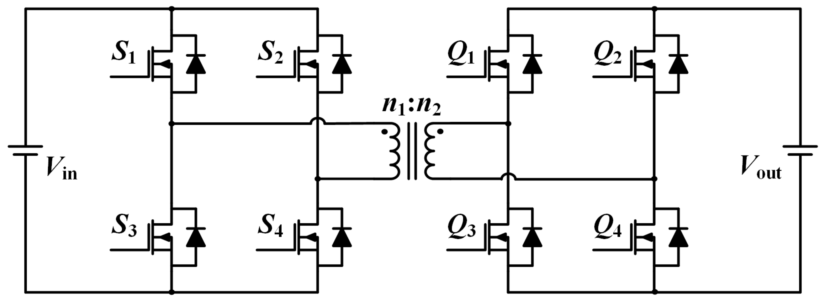
Figure 1.
The conventional full-bridge dual active bridge (DAB) converter.

Figure 2.
Conventional power balancing controller [28].
Figure 2.
Conventional power balancing controller [28].

Figure 3.
Conventional current sensorless power balancing controller [29].
Figure 3.
Conventional current sensorless power balancing controller [29].

Figure 4.
Configuration of the single-phase 5-level SST system.

Figure 5.
Transformer equivalent model with equivalent impedance referred to secondary side.

Figure 6.
Equivalent circuit of the proposed auto-balancing DAB converter.

Figure 7.
Six operation modes of the proposed auto-balancing topology during one switching cycle: (a) Mode I; (b) Mode II; (c) Mode III; (d) Mode IV; (e) Mode V; (f) Mode VI.
Figure 7.
Six operation modes of the proposed auto-balancing topology during one switching cycle: (a) Mode I; (b) Mode II; (c) Mode III; (d) Mode IV; (e) Mode V; (f) Mode VI.

Figure 8.
Theoretical waveforms of the proposed auto-balancing DAB converter when two inductances are different.
Figure 8.
Theoretical waveforms of the proposed auto-balancing DAB converter when two inductances are different.

Figure 9.
The expanded DAB model using common point connected transformers.

Figure 10.
The equivalent circuit when the number of modules is expanded: (a) three DAB modules with common-point-connected winding transformers (angle interval between 0 to ); (b) four DAB modules with common-point-connected winding transformers (angle interval between 0 to ).
Figure 10.
The equivalent circuit when the number of modules is expanded: (a) three DAB modules with common-point-connected winding transformers (angle interval between 0 to ); (b) four DAB modules with common-point-connected winding transformers (angle interval between 0 to ).

Figure 11.
Theoretical waveform when the number of modules is expanded: (a) theoretical waveform when employing three DAB modules; (b) theoretical waveform when employing four DAB modules.
Figure 11.
Theoretical waveform when the number of modules is expanded: (a) theoretical waveform when employing three DAB modules; (b) theoretical waveform when employing four DAB modules.

Figure 12.
Simulation waveforms of the 5-level SST when the two inductances are different: (a) when employing the proposed DAB topology; (b) when employing the conventional DAB converter, as presented in [28].
Figure 12.
Simulation waveforms of the 5-level SST when the two inductances are different: (a) when employing the proposed DAB topology; (b) when employing the conventional DAB converter, as presented in [28].

Figure 13.
Waveforms when the number of modules is expanded: (a) When three modules are used; (b) When four modules are used.
Figure 13.
Waveforms when the number of modules is expanded: (a) When three modules are used; (b) When four modules are used.

Figure 14.
The 5-level SST prototype system that employs the proposed auto-balancing DAB converter.

Figure 15.
Experimental waveforms of the 5-level CHB rectifier modules (rated 3 kW load condition).

Figure 16.
Steady-state waveforms of the proposed DAB converter: (a) waveforms of bridge voltages and inductor currents; (b) voltage and current waveforms of inductors.
Figure 16.
Steady-state waveforms of the proposed DAB converter: (a) waveforms of bridge voltages and inductor currents; (b) voltage and current waveforms of inductors.

Figure 17.
Experimental waveforms of balanced DC-links under various step load changes.

© 2018 by the authors. Licensee MDPI, Basel, Switzerland. This article is an open access article distributed under the terms and conditions of the Creative Commons Attribution (CC BY) license (http://creativecommons.org/licenses/by/4.0/).
Share and Cite
MDPI and ACS Style
Yun, H.-J.; Kim, H.-S.; Kim, M.; Baek, J.-W.; Kim, H.-J. A DAB Converter with Common-Point-Connected Winding Transformers Suitable for a Single-Phase 5-Level SST System. Energies 2018, 11, 928. https://doi.org/10.3390/en11040928
AMA Style
Yun H-J, Kim H-S, Kim M, Baek J-W, Kim H-J. A DAB Converter with Common-Point-Connected Winding Transformers Suitable for a Single-Phase 5-Level SST System. Energies. 2018; 11(4):928. https://doi.org/10.3390/en11040928
Chicago/Turabian StyleYun, Hyeok-Jin, Ho-Sung Kim, Myoungho Kim, Ju-Won Baek, and Hee-Je Kim. 2018. "A DAB Converter with Common-Point-Connected Winding Transformers Suitable for a Single-Phase 5-Level SST System" Energies 11, no. 4: 928. https://doi.org/10.3390/en11040928
Note that from the first issue of 2016, this journal uses article numbers instead of page numbers. See further details here.