New Switched-Dual-Source Multilevel Inverter for Symmetrical and Asymmetrical Operation


Electrical & Computer Engineering Department, Tuskegee University, Tuskegee, AL 36088, USA
*
Author to whom correspondence should be addressed.
Energies 2018, 11(4), 984; https://doi.org/10.3390/en11040984
Submission received: 10 March 2018
/
Revised: 8 April 2018
/
Accepted: 13 April 2018
/
Published: 18 April 2018
(This article belongs to the Special Issue Emerging Power Electronics Technologies for Power Systems and Machine Drives)
Abstract
:The increasing integration of large solar PV and wind farms into the power grid has fueled, over the past two decades, growing demands for high-power, high-voltage, utility-scale inverters. Multilevel inverters have emerged as the industry’s choice for megawatt-range inverters because of their reduced voltage stress, capability for generating an almost-sinusoidal voltage, built-in redundancy and other benefits. This paper presents a novel switched-source multilevel inverter (SS MLI) architecture. This new inverter shows superior capabilities when compared to existing topologies. It has reduced voltage stress on the semiconductor, uses fewer switches (i.e., reduced size/weight/cost) and exhibits increased efficiency. The proposed SS MLI is comprised of two voltage sources () and six switches. It is capable of generating five-level output voltage in symmetric mode (i.e., ) and seven-level output voltage in asymmetric mode (i.e., ). We present simulations results (using MATLAB®/Simulink®) for five- and seven-level output voltages, and they strongly support the validity of the proposed inverter. These positive results are further supported experimentally using a laboratory prototype.
1. Introduction
These past couple of decades have seen significant investments in renewable resources (RES) as a way to reduce the carbon footprint. In recent years, these initiatives have resulted in the installation of utility-scale wind and solar farms. The operations of such MW-scale plants require high-voltage/-power multilevel inverters (MLIs), and as a result, the usage of MLIs has proliferated [1,2]. MLIs can be categorized into three main types: neutral-point-clamped (NPC) [2,3], flying-capacitor (FC) [4,5] and cascaded H-bridge (CHB) topologies [6,7,8,9]. It should also be pointed out that some researchers have proposed hybrids of the above types [10,11]. The main advantages of MLIs over their traditional two-level counterparts are improved power quality, reduced filter requirements, lower electromagnetic interference and lower stress on loads [12,13].
A critical drawback of NPC topologies is the unbalance of the neutral point. This shortcoming leads to uneven thermal distribution in semiconductor devices, an increase in harmonics and a reduction of power quality [14]. FC inverters suffer from capacitor voltage imbalance issues, which lead to a deterioration of power quality and an increase in blocking voltages. The FC topology also requires larger capacitor banks and additional pre-charging circuitry. CHB MLIs suffer from input DC leakage current, which could damage PV panels, for example, and pose safety problems [15,16]. It is worth pointing out, however, that the CHB topology exhibits many advantages; namely, modularity, fewer number of components, symmetric or asymmetric operating modes (i.e., equal or unequal DC sources), etc.
In recent years, research on new MLIs has focused on topologies that require a minimal number of switches, diodes, gate drivers and DC sources as the number of voltage levels increases [7,8,9,17,18,19,20,21]. These new topologies try to minimize voltage stress on switches and the number of switches in the current path (losses). Many of the new CHB topologies rely on generating more voltage levels by using switched-capacitor (SC) or switched-source (SS) MLI configurations. SC MLIs [18,19] aim to produce more output voltage levels using a single or minimal number of power supplies in combination with a series of self-balancing capacitors. They suffer however from increased voltage stress on the switches and from power dissipation due to the increasing number of series diodes [18]. Several SS MLIs are proposed in [7,9,20,22]. Unlike the SC configuration where capacitors are switched in series/parallel combinations, the SS configuration achieves the voltage levels by using multiple DC sources.
The topologies presented in [20,21,23] completely eliminate the need for an H-bridge. The elimination of the H-bridge in addition to reducing the number of switches also help to minimize the uneven distribution of power losses among the switches without any specialized control algorithm.
This configuration is inherently suited for applications that have multiple DC sources, such as battery storage, solar PV or fuel cells. In the SS configuration, for the same number of components (sources, switches and passive devices), a higher number of voltage levels can be obtained in asymmetric topology (i.e., DC sources have different amplitudes) as compared to the asymmetric topology (i.e., DC sources have the same amplitudes) [24]. The current commutation path is generally shorter in the SS topology than in the SC topology; thereby, reducing power dissipation. Another advantage SS MLIs have over SC MLIs is their higher number of redundant switching states, which may be useful for certain control applications (e.g., fault-tolerant inverters).
In this paper, a new SS MLI topology is proposed. The new topology exhibits better performance, when compared to similar SS MLI topologies [7,17,25,26], in terms of the number of switches, current commutation path and voltage stress on the switches. The validity of the proposed topology is verified by MATLAB®/Simulink® simulations’ laboratory-scale experimental results. The rest of the paper is organized as follows: The structure and operation of the inverter are presented in Section 2. Comparisons of the discussed topologies are discussed in Section 3, and simulation results are presented in Section 4. Finally, conclusions are drawn in Section 5.
2. Architecture and Principle of Operation
2.1. Architecture
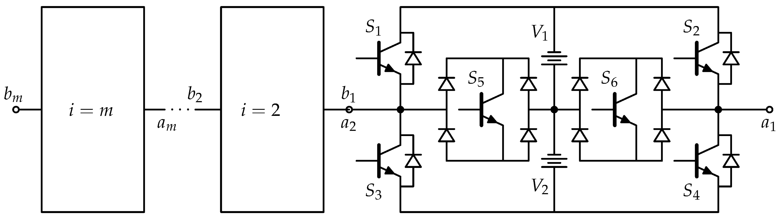
The basic unit of the proposed MLI (see Figure 1) is comprised of two DC power sources ( and ), four unidirectional switches (, , and ) and two bidirectional switches ( and ). This basic unit is capable of generating five-level output voltage (i.e., ), when (i.e., symmetric mode operation) and seven-level output voltage when (i.e., asymmetric mode operation).
The basic unit can be cascaded to generate more voltage levels. If m basic units are cascaded as shown in Figure 2, the inverter can generate up to and () voltage output levels for symmetric and asymmetric operations, respectively.
In order to avoid short-circuiting the DC power sources, only one of the left-side switches (i.e., , , ) can be ON at a given instant. Similarly, only one of the right-side switches (i.e., , , ) can be ON at a given time. Consequently,
where denotes the switching function of switch k () and takes the value of one when ON and zero when OFF. Based on (1), Table 1 shows the set of all possible switching states of the basic unit and the resulting inverter output voltage. The set of switching states consists of three null states (i.e., V) and six active states. The three redundant null states may be utilized to achieve different control objectives. However, the authors did not focus on that research aspect in this paper. The states shown in light-gray (i.e, all except 4) in Table 1 are the ones utilized in this work. The bidirectional switches protect the inverter from short-circuit currents when operating in asymmetrical mode.
Due to the voltage drop in each one of the diodes of the rectifier bridge (two diodes forward biased simultaneously, V), the use of bidirectional switches will distort the output waveform at low voltage levels. However, the issue becomes insignificant in medium and high voltage level applications.
2.2. Operation Principle
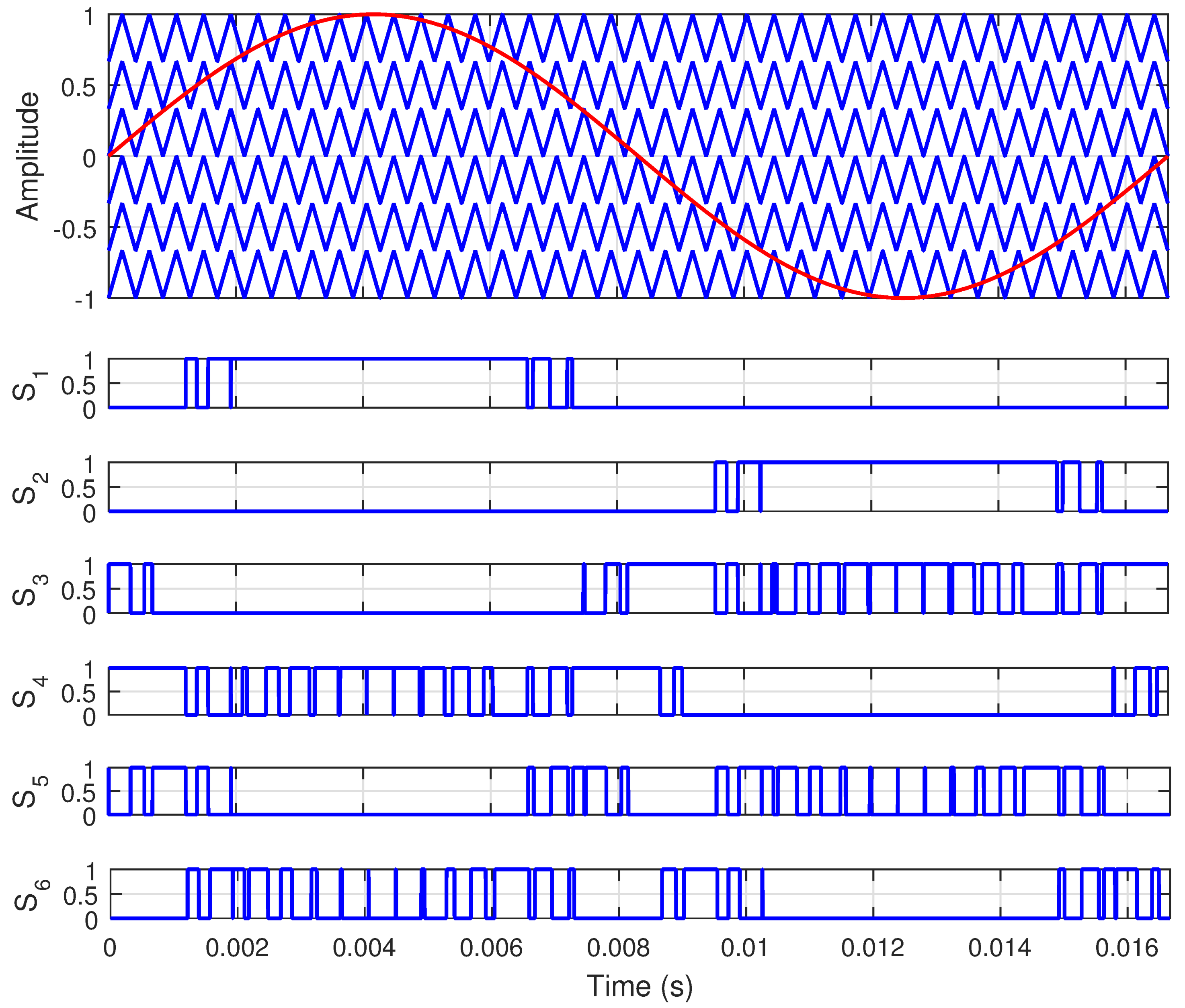
The generation of the multi-level voltage output is based on the switching states given in Table 1. For example, to produce a seven-level output (), at least one null state (i.e., States red or 9) and all the active states (i.e., red and red 8) are fired in-sequence. For uniform power dissipation among the six switches, two null states (i.e., red 1 and 9) are utilized, where Statered1 is ON during the positive half-cycle, whereas State 9 is used during the negative half-cycle. Although any PWM method may be used to control the semiconductor switches, we selected phase disposition PWM (PD-PWM) because of its superior performance [27]. The PD PWM is illustrated in Figure 3. The desired modulating signal is compared with high frequency triangular carrier signals to generate the gate signals.
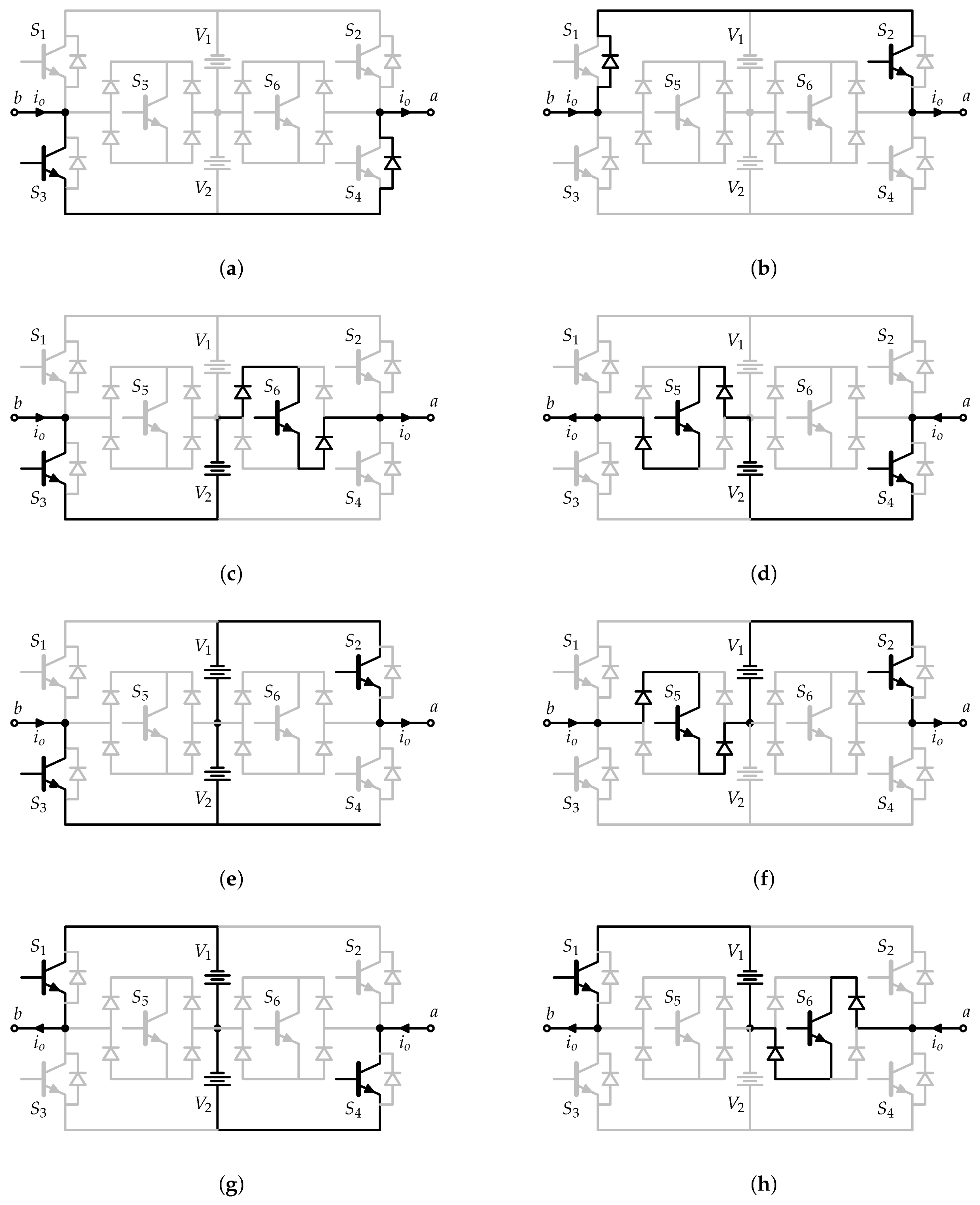
Figure 4 shows the current commutation for each switching state. For example, to produce in the positive half-cycle, switches and must be simultaneously turned ON (i.e., State in Table 1). Figure 4 shows the current path for the aforementioned scenario. Figure 4 shows the current commutations for all seven voltage levels. It should be noted that when , a maximum of five levels is achievable.
3. Comparison with Similar Topologies
In this section, the proposed topology is compared to the topologies presented in [25,26] and the conventional cascaded H-bridge topology discussed in [26]. Comparisons are made in terms of: (i) the total number of semiconductor devices; (ii) the number of active components in the current path (conduction losses); and (iii) the voltage stress that can be sustained by each switch.
3.1. Number of Semiconductor Devices
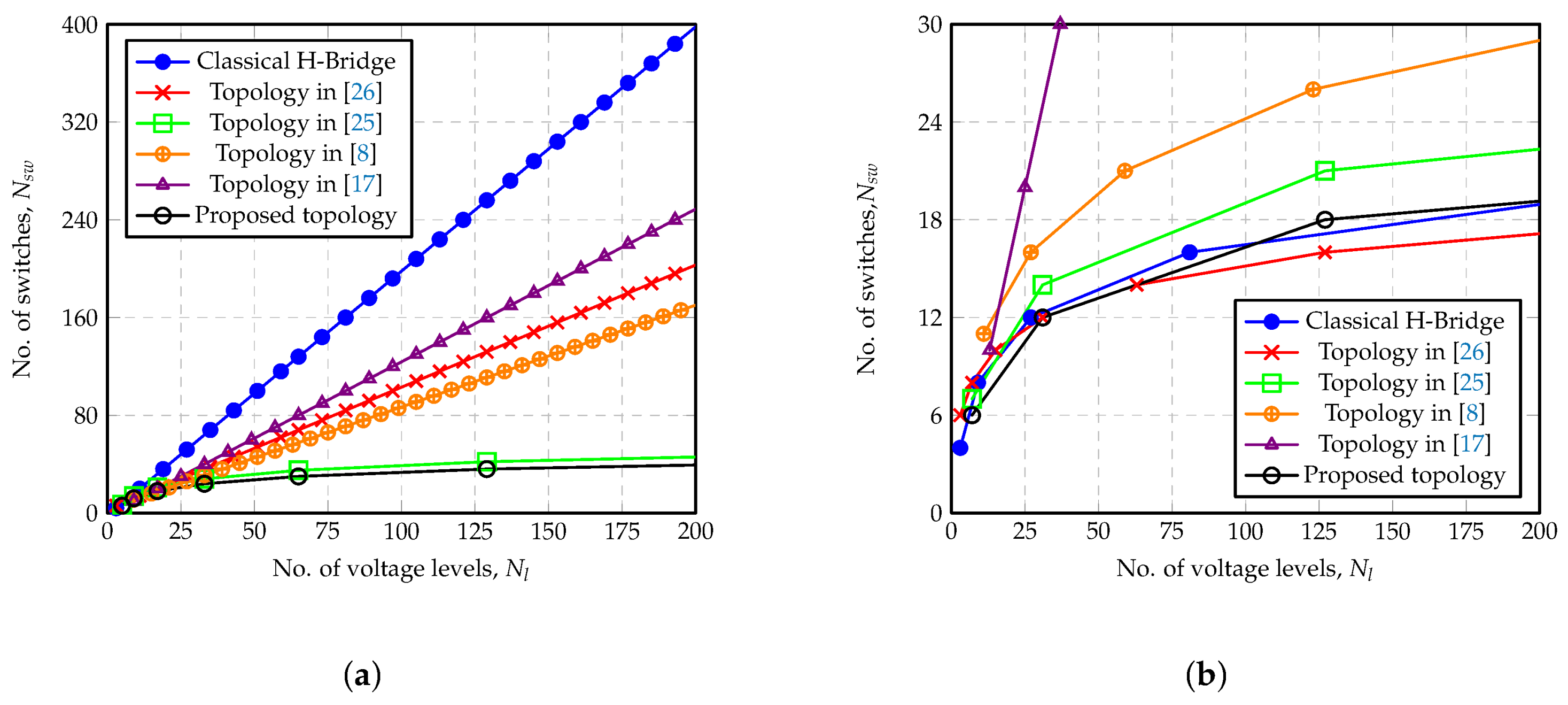
The number of semiconductor devices has an impact on the cost and size/weight of an MLI unit because the ability to generate the same number of voltage output levels by using less switches will both lower a unit’s cost and physical size. Figure 5a,b shows the number of switches () needed to generate the same number of voltage output levels () for different topologies in symmetric or asymmetric mode, respectively. In symmetric mode (Figure 5a), it is clear that the proposed topology outperforms the other three topologies with the lowest switch count for the same voltage level. In asymmetric mode (i.e., Figure 5b), however, the proposed topology fares better at lower voltage levels (), but this advantage diminishes at higher voltage levels.
3.2. Number of Semiconductors in the Current Path
Unlike in deal cases when we assume a switch or diode can turn on or turn off instantaneously without any power loss, real semiconductor switches have a finite switching transition time. This finite transition period is accompanied by power loss transients [28]. Hence, a smaller number of required switches to produce a voltage level implies reduced power losses. Figure 6a,b shows the number of switches in the current path for the same voltage levels for the different topologies in symmetric and asymmetric mode, respectively. The proposed topology performs better than in both operating modes and results in higher efficiency at any output voltage level.
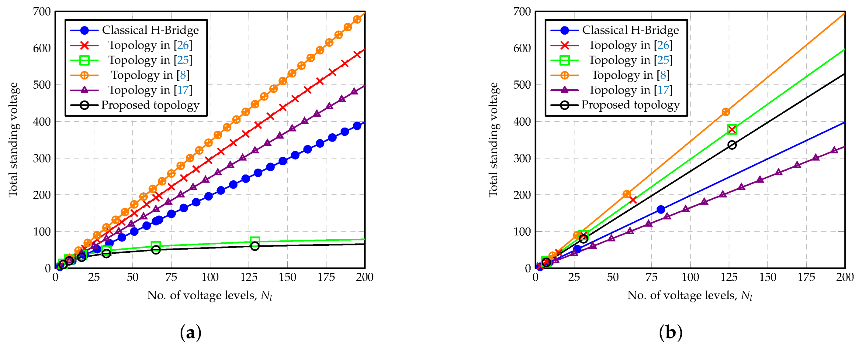
3.3. Total Standing Voltage
The minimum voltage rating of switches is another important factor that should be taken into consideration when comparing topologies. This minimum voltage rating, which has a direct influence on the price and size of the switches, is related to the voltage stress that the devices need to handle in blocking state. This phenomenon is also referred to as standing voltage. The total standing voltage is obtained by adding the blocking voltage requirement of each switch in a topology.
For the sake of comparison, we assumed that V. Figure 7a,b shows respectively the total standing voltage in symmetric and asymmetric modes for all the topologies. In both symmetric and asymmetric modes, it can be readily shown that the proposed topology outperforms all others topologies that have been evaluated.
4. Simulation and Experimental Results
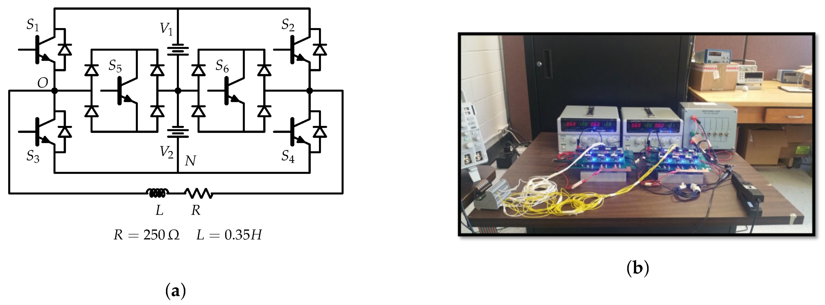
Figure 8a shows the schematic of the system under study, and the corresponding laboratory prototype is shown Figure 8b. Simulations were carried out using MATLAB/Simulink (R2015a, The MathWorks Inc., Natick, MA, USA). The semiconductor switches are IGBT IXGN120N60A3D1 with voltage and current ratings of 600 V, 120 A, respectively. The gate control signals were implemented using OPAL-RT OP5700 RCP/HIL FPGA-based Real-time Simulator. Two low-power DC sources were engaged in supplying the required voltages. Table 2 list the specifications of the inverter used for both the simulations and hardware experiment.
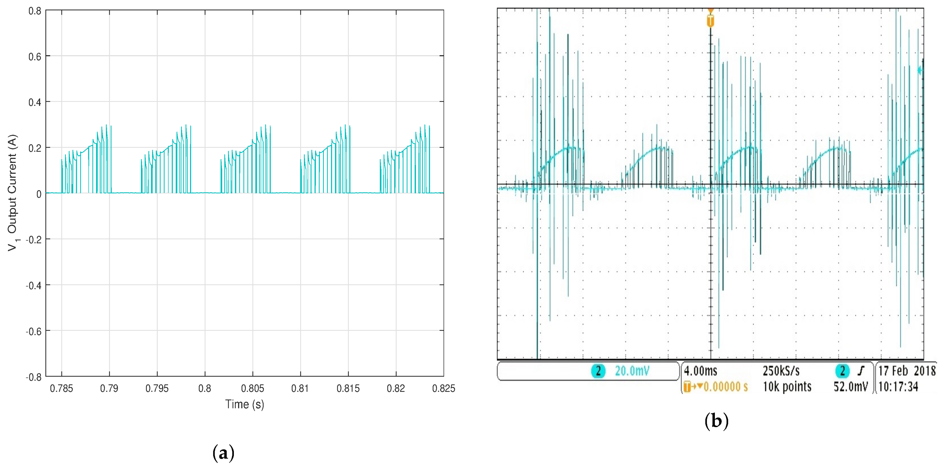
Figure 9a shows the simulation results of the converter output voltage and load current waveforms for five-level (symmetrical) operation. The THD of the voltage and current waveforms is and , respectively. The corresponding experimental waveforms for the symmetrical operations are shown in Figure 9b. The experimental waveforms confirm accurate five-level output voltage with an associated current waveform exhibiting small THD. Simulation and experimental results are also shown for the voltage across switch (i.e., ) and the current through the source . These are depicted in Figure 10 and Figure 11.
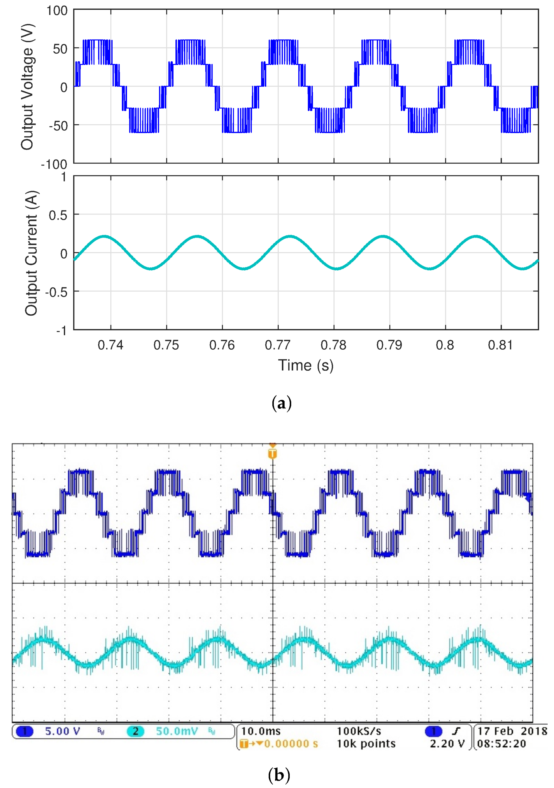
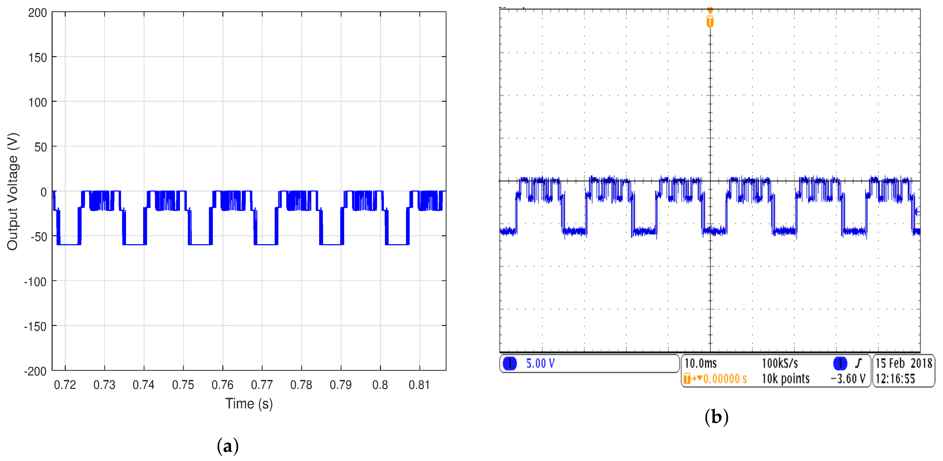
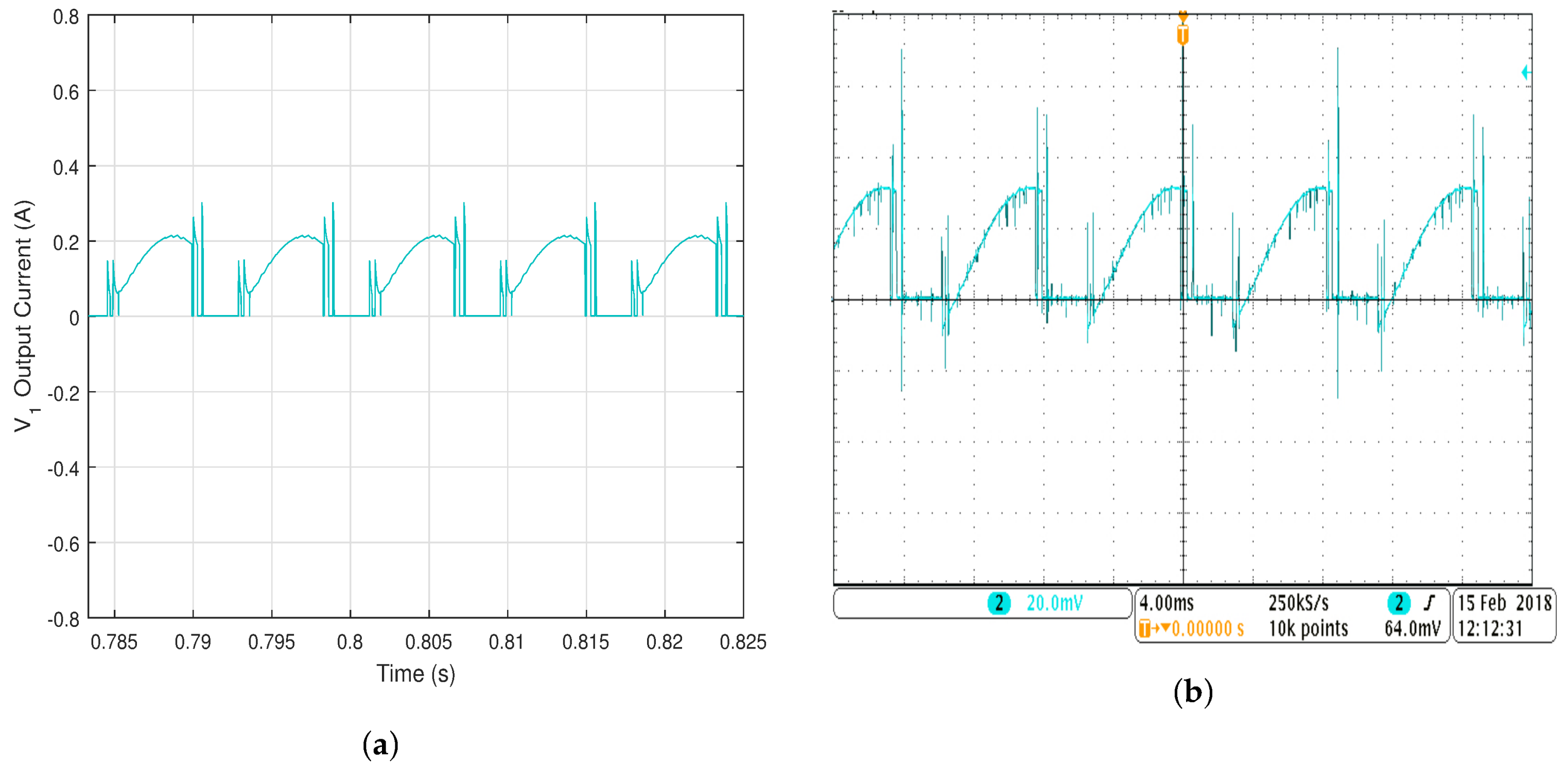
The results of the seven-level (asymmetrical) operation are presented in Figure 12, Figure 13 and Figure 14. Figure 12a shows simulated voltage and current waveforms, whilst Figure 12b presents the corresponding experimental waveforms. The THD of the voltage and current waveforms for the seven-level operation are and , respectively. As in the case of the symmetrical operation, the experimental waveforms confirm accurate seven-level output voltage, with an almost sinusoidal current waveform. Simulation and experimental waveforms for The switch voltage, , and the current through for the seven-level inverter are shown in Figure 13 and Figure 14, respectively. The presented results clearly verify the feasibility of the proposed inverter topology.
5. Conclusions
In this paper, we proposed a new topology for a switched-source multilevel inverter. The structure and operating principles of the design are discussed and validated using both theoretical simulations and hardware experiments. The basic unit can be operated in both symmetric and asymmetric modes. The new SS MLI topology is compared to four similar SS MLI topologies in terms of the number of switches required to generate a voltage level, the number of switches in the current path (power losses) and the total standing voltage that can be handled by the switches. From these comparisons, the proposed topology performs better than the other topologies for symmetrical operation for all the parameters being compared. However, for asymmetrical mode, the proposed topology shows better performance only on the number of switches in the current path (less losses). The proposed topology can be effectively employed for applications where series- and/or parallel-connected DC sources are available (e.g., in solar-PV/battery systems). The proposed topology produces both positive and negative voltage levels without the need for the classical H-bridge circuit and thus reduces the semiconductor device count. A limitation of the proposed inverter is the fact that it requires at least two voltage sources to operate. MATLAB/Simulink simulations and experiments using a laboratory prototype are presented for five- and seven-level (i.e., symmetric and asymmetric) operations, respectively.
Acknowledgments
This work was supported primarily by the ERC Program of the National Science Foundation and DOE under NSF Award Number EEC-1041877 and the CURENT Industry Partnership Program. The authors also want to express gratitude to Will Mefford who helped to produced the PCB for the inverter prototype.
Author Contributions
Cristopher Luciano and Kennedy Aganah conceived of and designed the experiments. Cristopher Luciano performed the experiments. Cristopher Luciano, Kennedy Aganah and Mandoye Ndoye wrote the paper. Gregory Murphy contributed supplies/simulation tools.
Conflicts of Interest
The authors declare no conflict of interest.
References
- Krug, D.; Busse, S.; Beuermann, M. Complete performance test of MV drive with modular multilevel topology for high power oil & gas applications. In Proceedings of the Petroleum and Chemical Industry Technical Conference (PCIC), Philadelphia, PA, USA, 19–22 September 2016; pp. 1–6. [Google Scholar]
- Ma, K.; Blaabjerg, F. Modulation methods for neutral-point-clamped wind power converter achieving loss and thermal redistribution under low-voltage ride-through. IEEE Trans. Ind. Electron. 2014, 61, 835–845. [Google Scholar] [CrossRef]
- Wang, J.; Gao, Y.; Weidong, J. A Carrier-Based Implementation of Virtual Space Vector Modulation for Neutral Point Clamped Three-Level Inverter. IEEE Trans. Ind. Electron. 2017, 64, 9580–9586. [Google Scholar] [CrossRef]
- Shimmyo, S.; Mochikawa, H.; Morishima, Y. Development of high power density converter using flying capacitor multilevel circuits for PV systems. In Proceedings of the 2016 19th IEEE International Conference on Electrical Machines and Systems (ICEMS), Chiba, Japan, 13–16 November 2016; pp. 1–6. [Google Scholar]
- Lei, Y.; Barth, C.; Qin, S.; Liu, W.C.; Moon, I.; Stillwell, A.; Chou, D.; Foulkes, T.; Ye, Z.; Liao, Z.; et al. A 2 kW, Single-Phase, 7-Level Flying Capacitor Multilevel Inverter with an Active Energy Buffer. IEEE Trans. Power Electron. 2017, 32, 8570–8581. [Google Scholar] [CrossRef]
- Babaei, E.; Laali, S.; Alilu, S. Cascaded multilevel inverter with series connection of novel H-bridge basic units. IEEE Trans. Ind. Electron. 2014, 61, 6664–6671. [Google Scholar] [CrossRef]
- Babaei, E.; Laali, S.; Bayat, Z. A single-phase cascaded multilevel inverter based on a new basic unit with reduced number of power switches. IEEE Trans. Ind. Electron. 2015, 62, 922–929. [Google Scholar] [CrossRef]
- Babaei, E.; Alilu, S.; Laali, S. A New General Topology for Cascaded Multilevel Inverters With Reduced Number of Components Based on Developed H-Bridge. IEEE Trans. Ind. Electron. 2014, 61, 3932–3939. [Google Scholar] [CrossRef]
- Mesquita, S.; Antunes, F.; Daher, S. A new bidirectional hybrid multilevel inverter with 49-level output voltage using a single dc voltage source and reduced number of on components. Electr. Power Syst. Res. 2017, 143, 703–714. [Google Scholar] [CrossRef]
- Fazel, S.S.; Bernet, S.; Krug, D.; Jalili, K. Design and comparison of 4-kV neutral-point-clamped, flying-capacitor, and series-connected H-bridge multilevel converters. IEEE Trans. Ind. Appl. 2007, 43, 1032–1040. [Google Scholar] [CrossRef]
- Naderi, R.; Smedley, K. A new hybrid active neutral point clamped flying capacitor multilevel inverter. In Proceedings of the 2015 IEEE Applied Power Electronics Conference and Exposition (APEC), Charlotte, NC, USA, 15–19 March 2015; pp. 794–798. [Google Scholar]
- Naderi, R.; Rahmati, A. Phase-Shifted Carrier PWM Technique for General Cascaded Inverters. IEEE Trans. Power Electron. 2008, 23, 1257–1269. [Google Scholar] [CrossRef]
- Mohan, D.; Kurub, S.B. A comparative analysis of multi carrier SPWM control strategies using fifteen level cascaded H-bridge multilevel inverter. Int. J. Comput. Appl. 2012, 41, 7–11. [Google Scholar]
- Du Toit Mouton, H. Natural balancing of three-level neutral-point-clamped PWM inverters. IEEE Trans. Ind. Electron. 2002, 49, 1017–1025. [Google Scholar] [CrossRef]
- Choi, H.; Zhao, W.; Ciobotaru, M.; Agelidis, V.G. Large-scale PV system based on the multiphase isolated dc/dc converter. In Proceedings of the 2012 3rd IEEE International Symposium on Power Electronics for Distributed Generation Systems (PEDG), Aalborg, Denmark, 25–28 June 2012; pp. 801–807. [Google Scholar]
- Villanueva, E.; Correa, P.; Rodríguez, J.; Pacas, M. Control of a single-phase cascaded H-bridge multilevel inverter for grid-connected photovoltaic systems. IEEE Trans. Ind. Electron. 2009, 56, 4399–4406. [Google Scholar] [CrossRef]
- Samadaei, E.; Gholamian, S.A.; Sheikholeslami, A.; Adabi, J. An envelope type (E-Type) module: asymmetric multilevel inverters with reduced components. IEEE Trans. Ind. Electron. 2016, 63, 7148–7156. [Google Scholar] [CrossRef]
- Taghvaie, A.; Adabi, J.; Rezanejad, M. A Self-balanced Step-up Multilevel Inverter based on Switched-Capacitor Structure. IEEE Trans. Power Electron. 2017, 33, 199–209. [Google Scholar] [CrossRef]
- Barzegarkhoo, R.; Kojabadi, H.M.; Zamiry, E.; Vosoughi, N.; Chang, L. Generalized structure for a single phase switched-capacitor multilevel inverter using a new multiple dc link producer with reduced number of switches. IEEE Trans. Power Electron. 2016, 31, 5604–5617. [Google Scholar] [CrossRef]
- Alishah, R.S.; Hosseini, S.H.; Babaei, E.; Sabahi, M. Optimal design of new cascaded switch-ladder multilevel inverter structure. IEEE Trans. Ind. Electron. 2017, 64, 2072–2080. [Google Scholar] [CrossRef]
- Prayag, A.; Bodkhe, S. Novel Basic Block of Multilevel Inverter Using Reduced Number of On-State Switches and Cascaded Circuit Topology. Adv. Electr. Eng. 2017, 2017, 1–16. [Google Scholar] [CrossRef]
- Chinnaiyan, V.K.; Shanmugam, P.K. A Multilevel Inverter topology using Single Source and Double Source Module with reduced Power Electronic Components. J. Eng. 2017, 2017, 139–148. [Google Scholar]
- Gupta, K.K.; Jain, S. A novel multilevel inverter based on switched DC sources. IEEE Trans. Ind. Electron. 2014, 61, 3269–3278. [Google Scholar] [CrossRef]
- Banaei, M.; Salary, E. Asymmetric Cascaded Multi-level Inverter: A Solution to Obtain High Number of Voltage Levels. J. Electr. Eng. Technol. 2013, 8, 316–325. [Google Scholar] [CrossRef]
- Ahmed, B.; Aganah, K.A.; Ndoye, M.; Arif, M.A.; Luciano, C.; Murphy, G.V. Single-phase cascaded multilevel inverter topology for distributed DC sources. In Proceedings of the 2017 IEEE 8th Annual Ubiquitous Computing, Electronics and Mobile Communication Conference (UEMCON), New York, NY, USA, 19–21 October 2017; pp. 514–519. [Google Scholar]
- Babaei, E.; Hosseini, S.H. New cascaded multilevel inverter topology with minimum number of switches. Energy Convers. Manag. 2009, 50, 2761–2767. [Google Scholar] [CrossRef]
- Xiao, M.; Xu, Q.; Ouyang, H. An Improved Modulation Strategy Combining Phase Shifted PWM and Phase Disposition PWM for Cascaded H-Bridge Inverters. Energies 2017, 10, 1327. [Google Scholar] [CrossRef]
- Lakkas, G. MOSFET power losses and how they affect power-supply efficiency. Analog Appl. 2016, 10, 22–26. [Google Scholar]
Figure 1.
Structure of the proposed topology as a standalone.
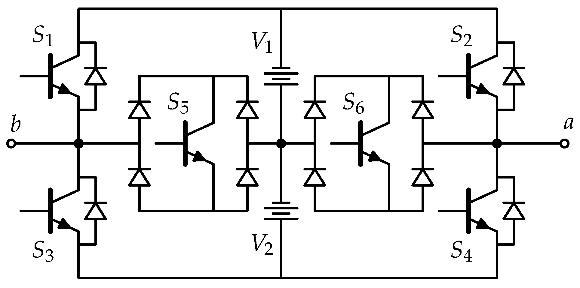
Figure 2.
m cascaded units to generate more voltage levels.

Figure 3.
Phase disposition (PD) modulation strategy and gate signals for seven-level inverter.

Figure 4.
Schematics of switching states for generating different levels in the output voltages (see Table 1): (a) state 1 for ; , (b) state 9 for ; , (c) state 2 for ; , (d) state 3 for ; , (e) state 5 for ; , (f) state 6 for ; , (g) state 7 for ; , and (h) state 8 for ; .
Figure 4.
Schematics of switching states for generating different levels in the output voltages (see Table 1): (a) state 1 for ; , (b) state 9 for ; , (c) state 2 for ; , (d) state 3 for ; , (e) state 5 for ; , (f) state 6 for ; , (g) state 7 for ; , and (h) state 8 for ; .

Figure 5.
Number of switches vs. output voltage levels of the proposed inverter compared to the three other topologies in (a) symmetric mode and (b) asymmetric mode.
Figure 5.
Number of switches vs. output voltage levels of the proposed inverter compared to the three other topologies in (a) symmetric mode and (b) asymmetric mode.

Figure 6.
Number of switches in the current path vs. the output voltage level of proposed inverter compared to the other three topologies in (a) symmetric mode and (b) asymmetric mode.
Figure 6.
Number of switches in the current path vs. the output voltage level of proposed inverter compared to the other three topologies in (a) symmetric mode and (b) asymmetric mode.
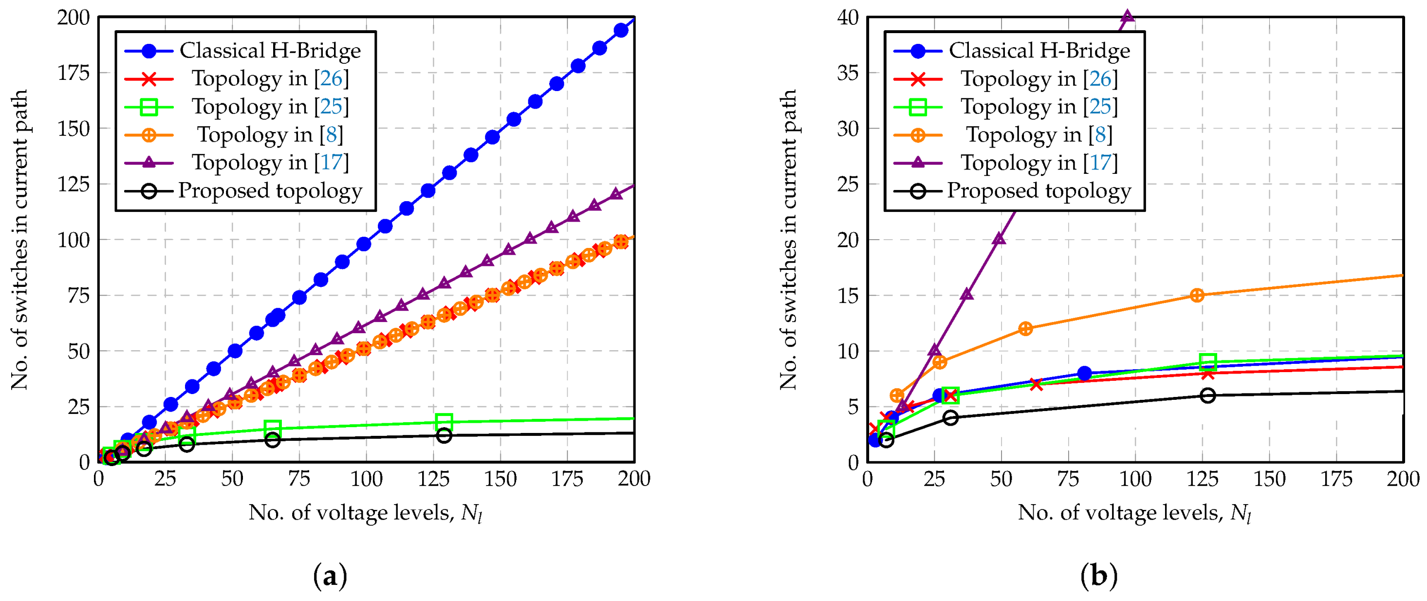
Figure 7.
Total standing voltage vs. output voltage levels of the proposed inverter compared to the other three topologies in (a) symmetric mode and (b) asymmetric mode.
Figure 7.
Total standing voltage vs. output voltage levels of the proposed inverter compared to the other three topologies in (a) symmetric mode and (b) asymmetric mode.

Figure 8.
Experimental test setup: (a) circuit and (b) picture of the laboratory test setup.

Figure 9.
Results of five-level switched-source multilevel inverter (SS MLI): (a) simulated output voltage (top) and load current; (b) experimental output voltage (top, 25 V/div) and current (bottom, 0.25 A/div).
Figure 9.
Results of five-level switched-source multilevel inverter (SS MLI): (a) simulated output voltage (top) and load current; (b) experimental output voltage (top, 25 V/div) and current (bottom, 0.25 A/div).

Figure 10.
Results of five-level SS MLI: (a) simulated voltage; (b) experimental voltage.
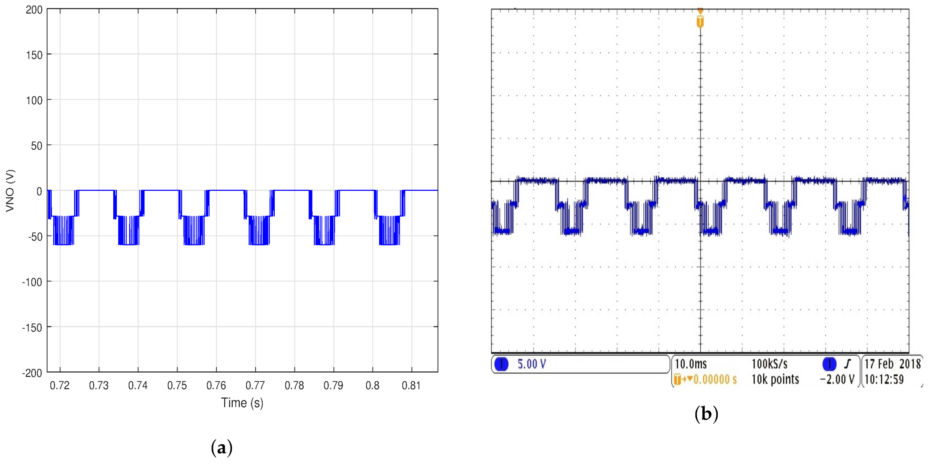
Figure 11.
Results of five-level SS MLI: (a) simulated source, , DC current; (b) experimental source, DC current.
Figure 11.
Results of five-level SS MLI: (a) simulated source, , DC current; (b) experimental source, DC current.

Figure 12.
Results of seven-level SS MLI: (a) simulated output voltage (top) and load current; (b) experimental output voltage (top, 25 V/div) and load current (bottom, 0.25 A/div).
Figure 12.
Results of seven-level SS MLI: (a) simulated output voltage (top) and load current; (b) experimental output voltage (top, 25 V/div) and load current (bottom, 0.25 A/div).
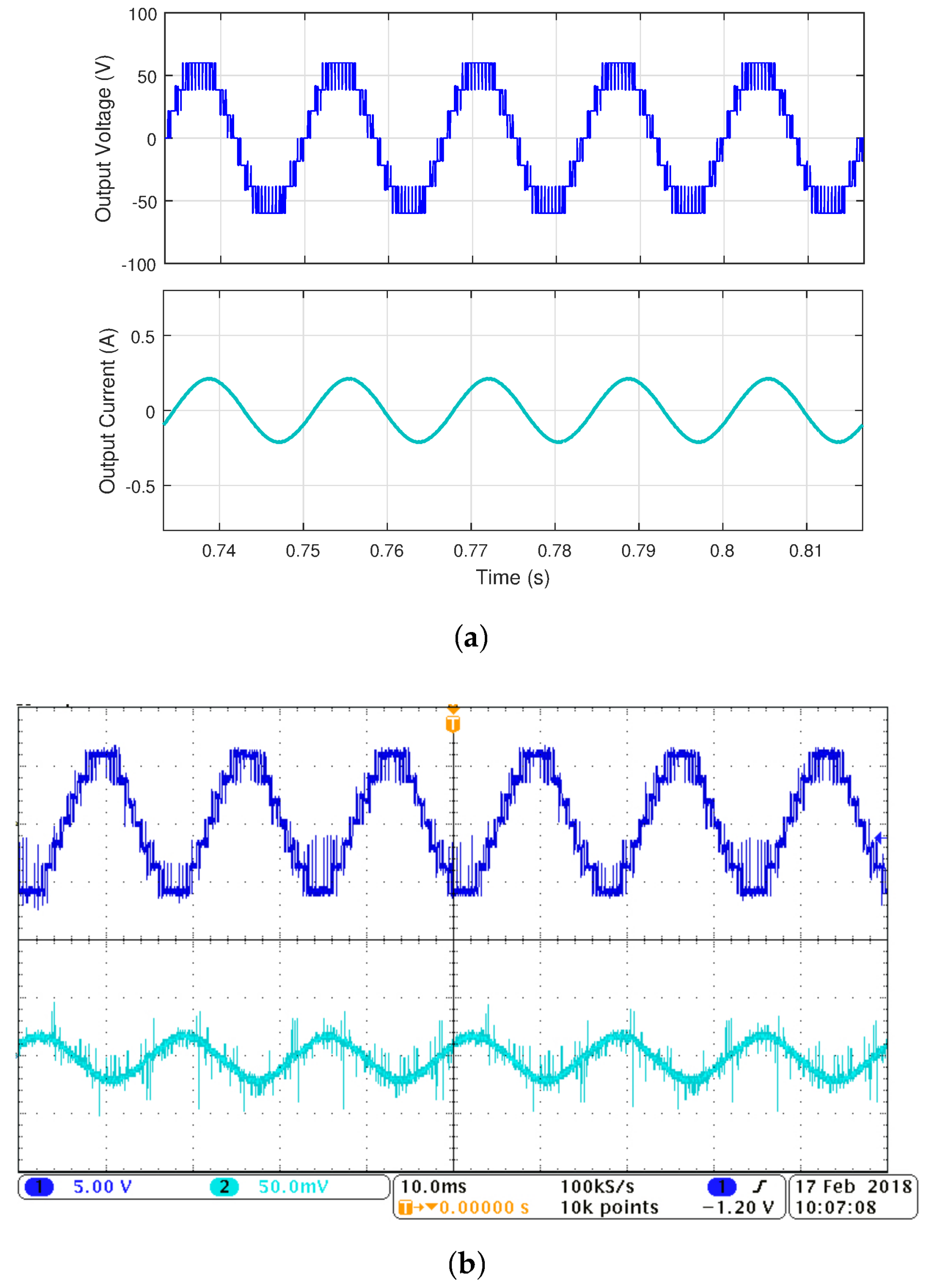
Figure 13.
Results of seven-level SS MLI: (a) simulated voltage; (b) experimental voltage.

Figure 14.
Results of seven-level SS MLI: (a) simulated source, , DC current; (b) experimental source, , DC current.
Figure 14.
Results of seven-level SS MLI: (a) simulated source, , DC current; (b) experimental source, , DC current.


Table 1.
Switching states for the basic unit. The states in light gray are used in this paper.
| States | |||||||
|---|---|---|---|---|---|---|---|
| 1 | 0 | 0 | 1 | 1 | 0 | 0 | 0 |
| 2 | 0 | 0 | 1 | 0 | 0 | 1 | |
| 3 | 0 | 0 | 0 | 1 | 1 | 0 | |
| 4 | 0 | 0 | 0 | 0 | 1 | 1 | 0 |
| 5 | 0 | 1 | 1 | 0 | 0 | 0 | |
| 6 | 0 | 1 | 0 | 0 | 1 | 0 | |
| 7 | 1 | 0 | 0 | 1 | 0 | 0 | |
| 8 | 1 | 0 | 0 | 0 | 0 | 1 | |
| 9 | 1 | 1 | 0 | 0 | 0 | 0 | 0 |
Table 2.
Parameters for 7-level and 31-level simulations.
| Parameter | Value |
|---|---|
| Frequency f | 60 Hz |
| Switching frequency | 2340 Hz |
| Modulation index | |
| DC power sources (5-level) | V V |
| DC power sources (7-level) | V V |
| Load | mH |
© 2018 by the authors. Licensee MDPI, Basel, Switzerland. This article is an open access article distributed under the terms and conditions of the Creative Commons Attribution (CC BY) license (http://creativecommons.org/licenses/by/4.0/).
Share and Cite
MDPI and ACS Style
Aganah, K.A.; Luciano, C.; Ndoye, M.; Murphy, G. New Switched-Dual-Source Multilevel Inverter for Symmetrical and Asymmetrical Operation. Energies 2018, 11, 984. https://doi.org/10.3390/en11040984
AMA Style
Aganah KA, Luciano C, Ndoye M, Murphy G. New Switched-Dual-Source Multilevel Inverter for Symmetrical and Asymmetrical Operation. Energies. 2018; 11(4):984. https://doi.org/10.3390/en11040984
Chicago/Turabian StyleAganah, Kennedy Adinbo, Cristopher Luciano, Mandoye Ndoye, and Gregory Murphy. 2018. "New Switched-Dual-Source Multilevel Inverter for Symmetrical and Asymmetrical Operation" Energies 11, no. 4: 984. https://doi.org/10.3390/en11040984
Note that from the first issue of 2016, this journal uses article numbers instead of page numbers. See further details here.