1. Introduction
As the fields of power semiconductor technology and power converter technology have advanced and interest in environmental pollution has increased, a distributed power source utilizing new and renewable energy has been attracting attention, and DC distribution has been actively studied for this purpose. DC distribution can be effectively connected to renewable energy sources and it can form an efficient power grid [
1,
2,
3]. Therefore, it is being applied in many applications, such as smart grids, internet data center (IDC), commercial buildings, and etc. [
4,
5,
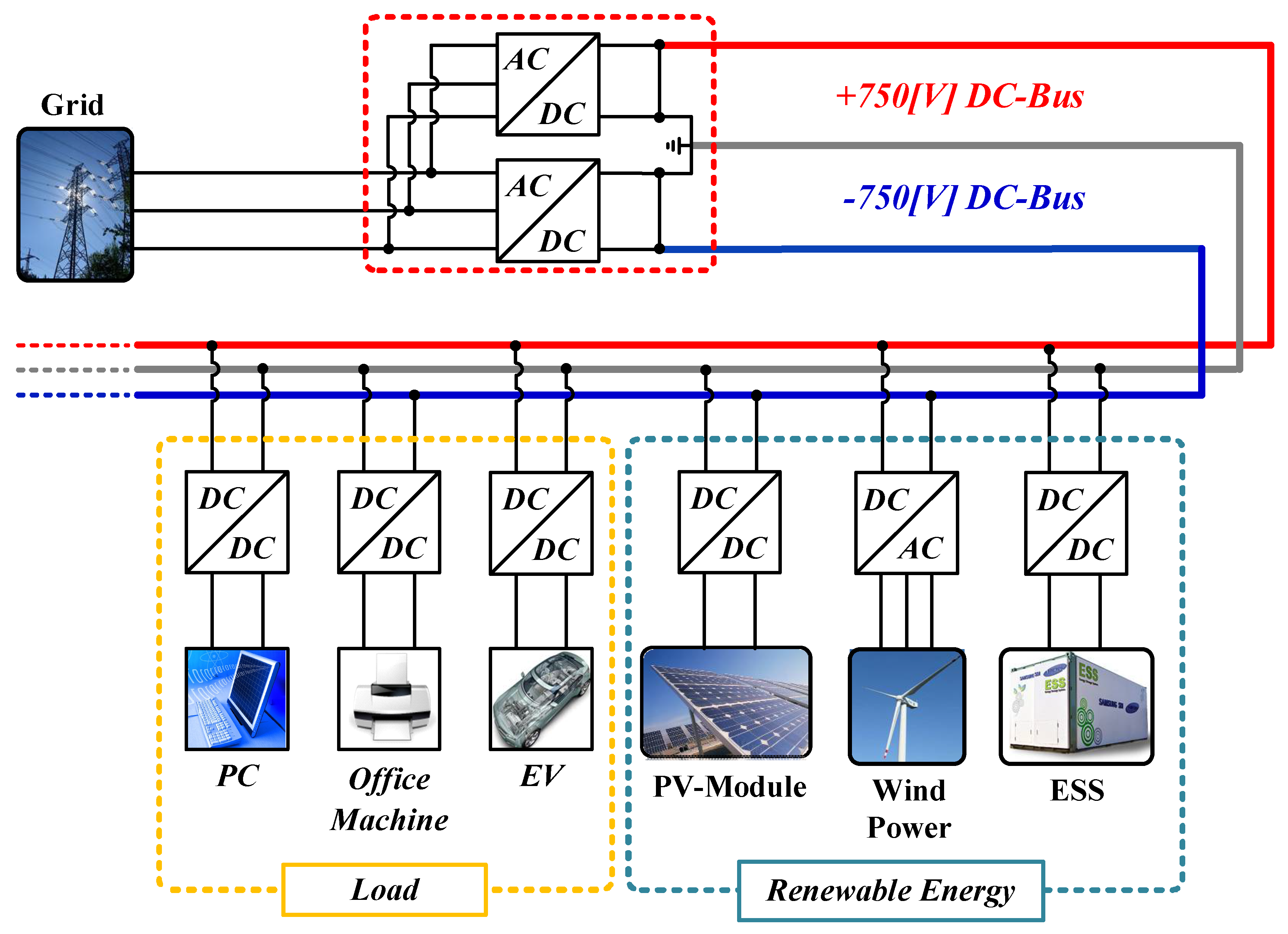
6]. The DC distribution is configured as shown in
Figure 1. Loads connected to the DC distribution are mostly nonlinear electronic loads such as lighting, computers, energy storage systems (ESS), and variable speed driving inverters for air conditioners, and these loads are sensitive to voltage fluctuations in the DC distribution [
7,
8,
9].
Because AC/DC power conversion system (PCS) are essential in maintaining the existing AC system and constructing a separate DC distribution, research into how to apply various topologies in various fields has already been conducted [
10,
11]. The three-phase AC/DC PCS is particularly advantageous in that the power factor is controllable and that the power flow is bidirectional when compared to a diode rectifier. Therefore, AC/DC PCS is adopted in applications where less distortion is required in the AC current waveform in order to meet the stringent regulations for the electrical harmonic quality of the AC system. Since the AC/DC PCS can control not only the magnitude of the current, but also the phase, the power factor can be controlled through the phase information of the AC system. Moreover, the DC link voltage can be controlled by controlling the input power [
12,
13].
Generally, space vector pulse width modulation (SVPWM) is applied to generate a switching signal in AC/DC PCS applying voltage oriented control (VOC) [
14,
15,
16]. In SVPWM, the maximum magnitude of the voltage that each vector can output varies in proportion to the voltage of the DC link (DC distribution voltage in this case). Therefore, if the DC link voltage fluctuates, the magnitude of the output voltage fluctuates as well. This is particularly true in a DC distribution system that is constructed using AC/DC PCS where the load is centralized, and power is generated/stopped from various renewable energy sources or nonlinear load is frequently connected/disconnected. This also causes a transient state of the DC distribution voltage, which refers to a fluctuation of the DC link voltage of the AC/DC converter. Also, DC-link voltage can be changed by AC voltage and current dips [
17,
18,
19,
20,
21]. A robust DC voltage control characteristic of AC/DC PCS is required to supply power to the sensitive load (to voltage fluctuation) that is connected to the DC distribution in a stable manner.
There have been several studies regarding the robust DC voltage control characteristics [
22,
23,
24]. In regards to robust DC distribution voltage, the method of applying Droop Control to all power converters connected to a DC distribution was studied in [
25,
26,
27,
28]. However, voltage ripple according to the droop curve always appears in voltage control of a DC distribution using droop control, and strict regulation is necessary for applying the droop curve for every device that is connected to the DC distribution. Therefore, a study was conducted to improve the robustness of droop control using model predictive control in [
29]. However, a complex control loop must be constructed to improve the control performance in order to implement the control method proposed in [
29]. It is also impossible to predict and model all of the loads connected to the DC grid in terms of maintaining power and the supply of power.
Therefore, the most reliable way to increase the robustness and dynamics characteristic of DC distribution is to improve the performance of AC/DC PCS and feedforward compensated to the output through the value that was obtained through modeling of the AC/DC PCS system [
30].
Meanwhile, a control method for voltage stabilization of the DC link voltage is studied in [
19,
20,
21] when voltage dips occur on the AC side voltage. The control method of improving control performance by adding a feedforward compensation term to the
d-
q axis current controller was applied in [
20,
21]. In this method, however, AC that was connected to PCS cannot control the Power Factor of the AC side clearly.
In this paper, a feed forward compensation method is proposed for robust DC voltage control characteristic of AC/DC PCS configuring the DC distribution network. The system applying the proposed compensation method improved control performance not only in the transient state occurring in the DC grid, but also in the AC voltage dip. The configuration of the DC distribution is reviewed and SVPWM is analyzed to propose compensation method for improving the DC-link voltage control for applying the proposed method. The DC distribution system that is applied in the proposed compensation method is modeled and compared with the conventional DC distribution system model in terms of stability. Moreover, simulation and experimentation were carried out to verify the validity of the proposed method.
2. Feedforward Compensation Method for Transient State Output Voltage
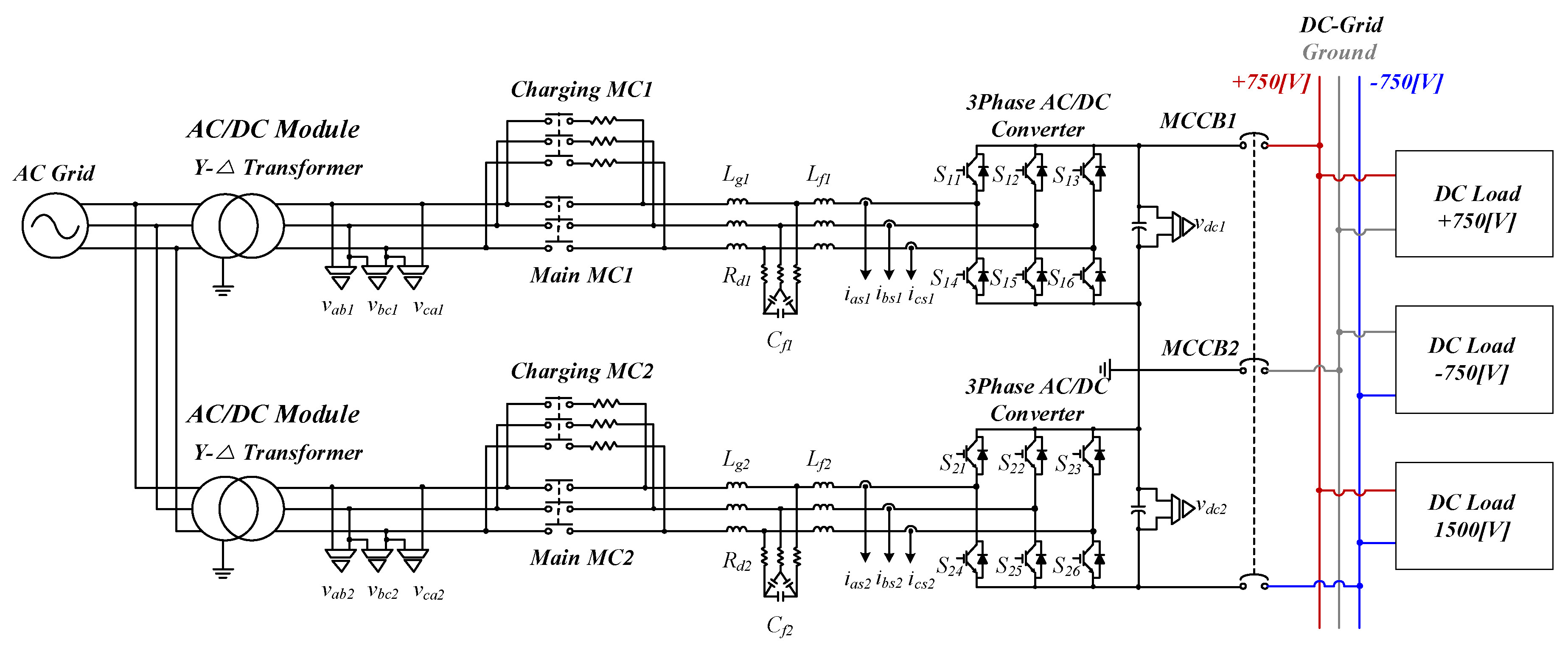
The circuit diagram of the DC distribution system that is used in this paper is shown in
Figure 2. The overall system consists of a bidirectional two-level AC/DC PCS module in series. Each module is configured with an initial charge circuit, LCL filter. The output voltage of each module is 750 V
dc and the total voltage is 1500 V
dc. The initial charging circuit of each module was applied to limit the inrush current, which can cause damages of the IGBT and the output capacitor due to the low impedance of the DC link capacitor at startup. The resistance (
Rpre) that is applied to the initial charging circuit was designed by the RC time constant with the DC link capacitor. The LCL filter has a smaller volume and inductance value than the L filter and the LC filter, also having a large harmonic attenuation effect. It is designed according to the considerations of system capacity, impedance, switching frequency, filter cut-off frequency, etc. As a tertiary passive filter, resonance may occur between the elements of the filter at specific frequencies on the LCL filter. In order to minimize this resonance, many studies have been conducted, but the passive damping method is applied in this paper [
31,
32].
The top power conversion module and the bottom power conversion module control the output voltage +750 Vdc as separate power converters, respectively. The voltage Vdc1 of the upper capacitor and the voltage Vdc2 of the lower capacitor do not affect each other because the closed circuit is not formed, even if the bipolar load power is unbalanced. Therefore, the simplicity of the control and the reliability of the system can be improved since the balancing control using a neutral point is no longer necessary. Due to various voltages, it can be used according to the purpose and the capacity of the load.
AC distribution systems, allow up to a voltage variation of ±10% from the reference voltage as a steady voltage, thus AC loads have robust characteristics against voltage fluctuations. However, the loads that are in the next-generation DC distribution systems are mostly composed of electronic loads sensitive to voltage fluctuations. Therefore, a new compensation technique is proposed for transient conditions in DC distribution systems to satisfy high power quality and stable voltage regulation for sensitive loads when considering the distribution systems that are connected with irregular renewable energy generation.
2.1. Relation to Transient State and Voltage Vector
In the AC/DC PCS, a PI voltage controller for DC link voltage control and a PI current controller for AC current control are used in series. The voltage of the DC link is indirectly controlled by controlling the 3-phase AC current and the power factor. The AC/DC PCS has an output dc link consisting of a capacitor, which causes an instantaneous undershoot due to dv/dt of the dc link capacitor when the load is connected or the power generation of the distributed power supply suddenly decreases. On the contrary, an overshoot occurs on the DC distribution voltage instantaneously when the connection of a load using a constant power is suddenly disconnected or when the distributed power has to regenerate the generated power to the system due to an instantaneous increase of power generation.
As a method of minimizing the overshoot and undershoot, the transient response of the converter can be improved through the power feedforward control by receiving information of load and renewable energy generation power in real time. However, it is practically impossible to collect the information of the power input/output status of all the loads that are connected to the power distribution through such communication. Therefore, compensation for this transient condition must be made in an AC/DC PCS that forms a DC distribution.
The voltage vector of AC/DC PCS using SVPWM is affected by fluctuations in the DC distribution voltage (i.e., DC link voltage of the AC/DC PCS) in this transient state when the converter controls the AC side pulse width modulation (PWM) output. Therefore, voltage vectors of SVPWM should be analyzed in both the steady state and transient state.
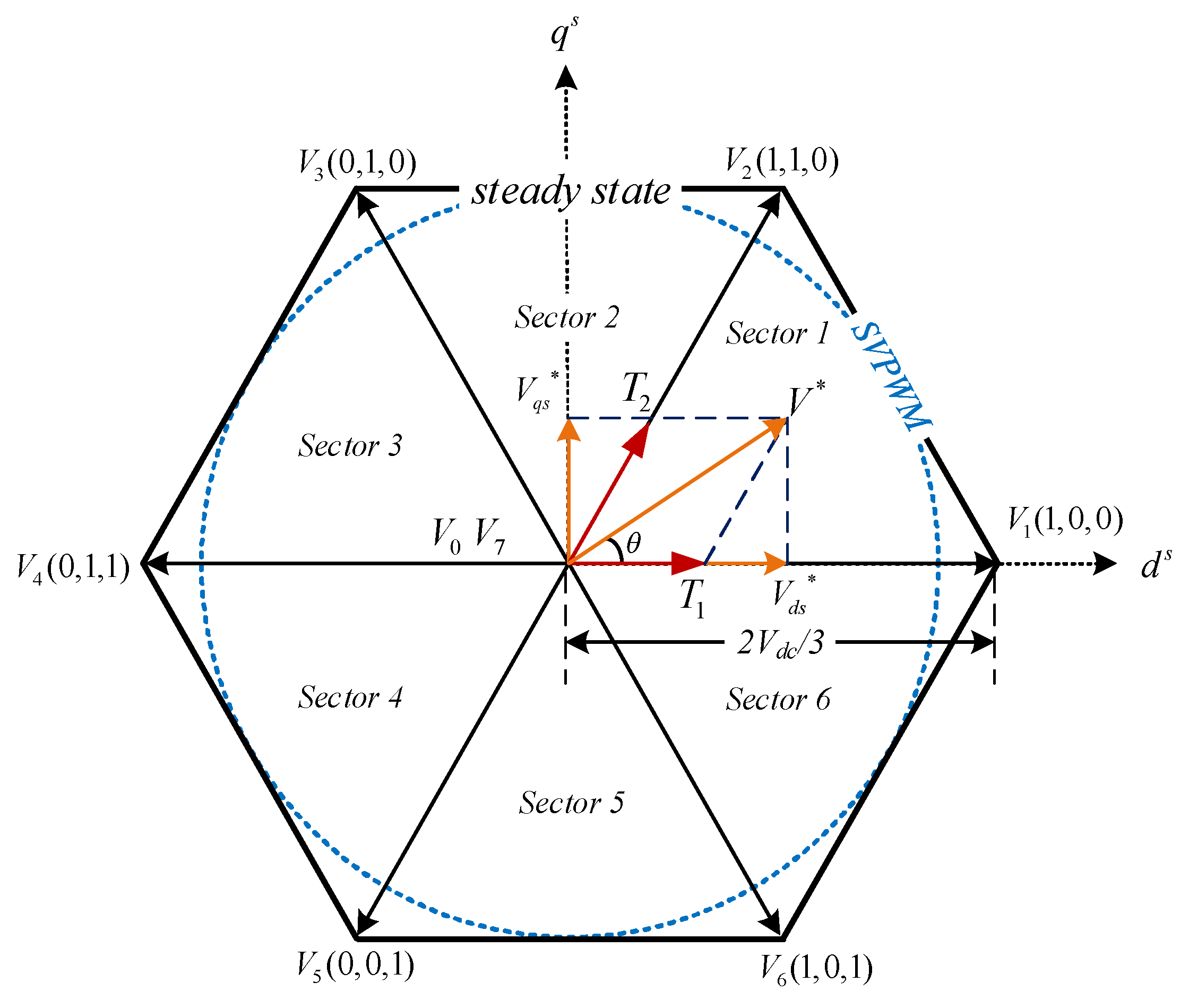
2.2. Space Vector Pulse Width Modulation (SVPWM) in Steady State
The vector diagram of SVPWM in steady state is represented, as shown in
Figure 3. The V
1 to V
6 are output voltage vectors from AC/DC PCS. These vectors are each phase-shifted by 60° and their magnitude is proportional to the DC link voltage of the converter to 2
Vdc/3.
The V
0 and V
7 vectors are referred to as zero voltage vectors because no actual voltage is output to the AC side load. The maximum output voltage of an inverter that can be linearly output in the SVPWM is equal to the radius of the circle that is inscribed in hexagon of
Figure 3 [
18,
19,
20,
21].
The SVPWM selects two adjacent valid vectors on the space vector in order to generate the command voltage and calculates the time each vector is applied. The applying time of two valid vectors are calculated, as shown in Equations (1)–(3) using the switching period.
The time when two vectors adjacent to the command voltage vector are applied by the Equations (1)–(3) is proportional to the maximum voltage (=2Vdc/3) that each vector can output. However, when T1, T2, and T0 are calculated to follow the reference voltage, according to Equations (1)–(3), if the voltage of the DC link changes, then T1, T2, and T0 also change. T1, T2, and T0 are changed when transient voltage occurs in the DC link of the AC/DC PCS (i.e., the DC distribution voltage). If the voltage of the DC link increases, T1, T2, and T0 must be calculated as smaller than the steady state in order to reach the reference voltage again for a fast response. When the voltage of the DC link decreases, T1, T2, T0 must be increased when compared to the steady state. Therefore, the time to apply the adjacent vector in the currently used SVPWM should be changed according to the voltage change in the DC-link.
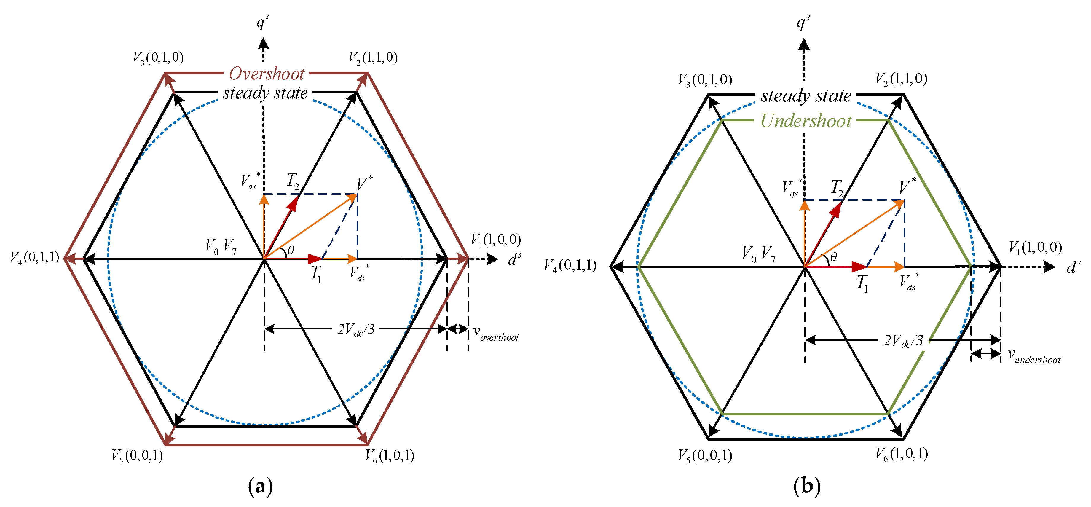
2.3. SVPWM Analysis in Transient State
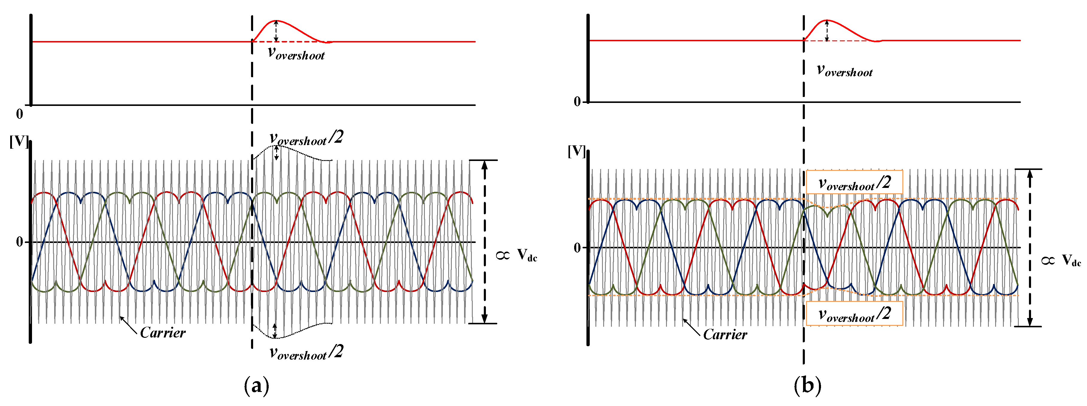
In the steady state, the maximum value of V
1–V
6 is fixed at 2
Vdc/3. However, when an overshoot or undershoot occurs in the output voltage, as shown in
Figure 4, the maximum voltage that can be output by the six vectors changes. When an overshoot occurs, the maximum output voltage of each vector increases by
and decreases by
when an undershoot occurs. This relationship is shown in the following equations.
According to Equations (4)–(6), the maximum value of two adjacent vectors changes when an overshoot or undershoot occurs. Therefore, the switching time for generating the reference voltage should be changed as shown in Equations (7)–(9).
Therefore, the switching time calculated from Equations (1)–(3) and (7)–(9) has an error. The error in Sector 1 is shown in Equations (10) and (11).
When the switching time is calculated as in the conventional method in Equations (1)–(3), the response characteristic due to the error is worsened when the transient state occurs. Therefore, it is desired to minimize this error by improving the transient response characteristics.
2.4. Feedforward Compensation Method of Output Voltage
The output of SVPWM is compared with the carrier wave in order to determine the switching pattern. The y-axis of the carrier wave refers to the voltage of the output capacitor (=). Therefore, when an overshoot or undershoot occurs, the maximum output value of each vector changes in the space voltage vector diagram, so that an error occurs in the output voltage of the three-phase inverter, according to Equations (1)–(11).
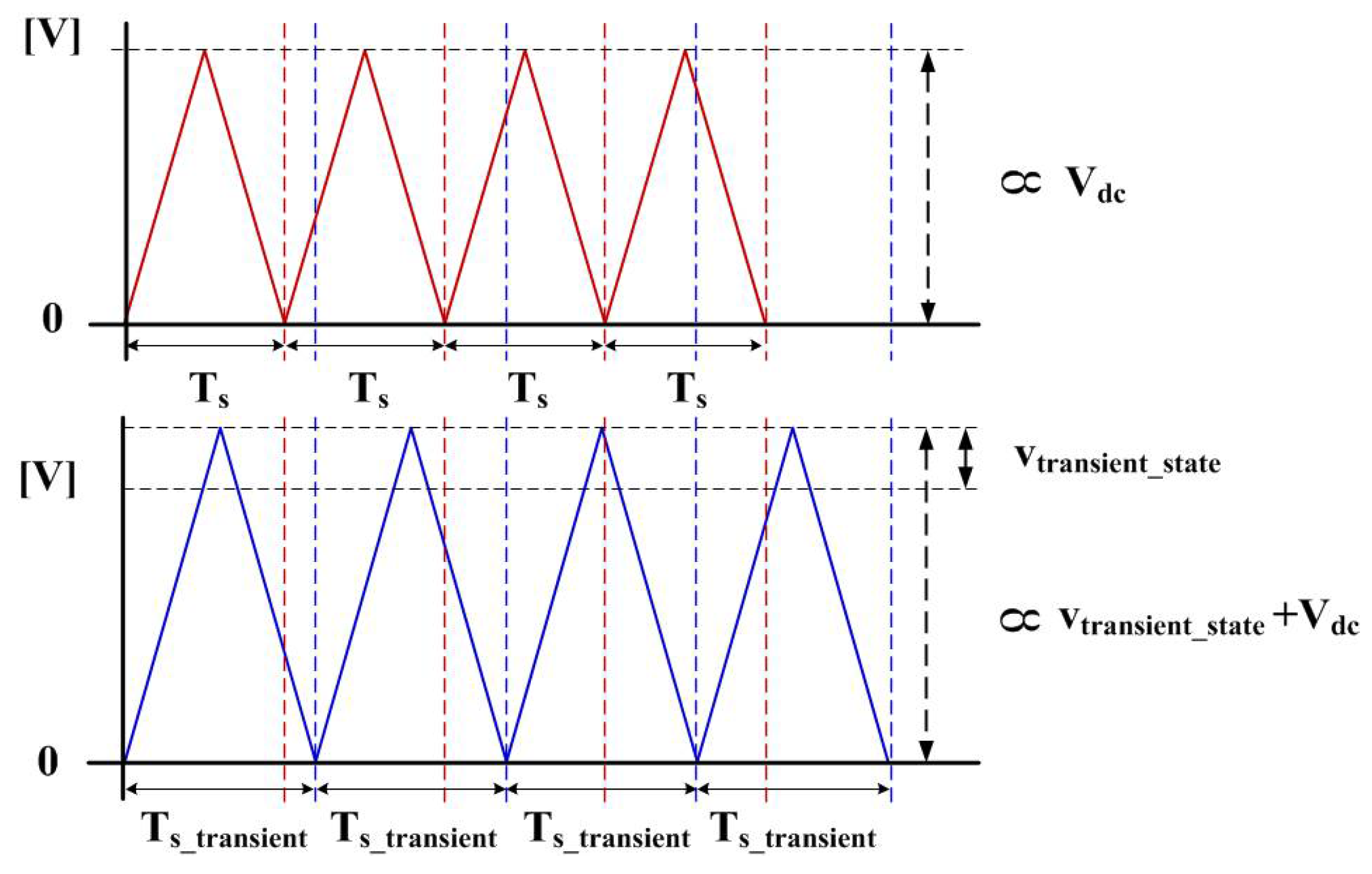
The relation between switching frequency and carrier waveform in a micro controller unit (MCU) is shown in
Figure 5. Generally, a method of changing the value (
y-axis) of the carrier waveform is used to compensate for the error. However, when generating the carrier waveform in the MCU, the slope of the carrier waveform is fixed according to the dividing ratio of the MCU. Therefore, if the maximum size (
y-axis) of the carrier waveform changes, the switching period changes as well. According to Equations (1)–(3) and (7)–(9), the switching time is affected by one period (=
) of the carrier frequency, so compensation using the carrier waveform cannot be accomplished at the same switching frequency. The switching frequency is changed if the conventional compensation method is used when an overshoot or undershoot occurs, which aggravates the total harmonic distortion (THD) characteristic of the ac side current.
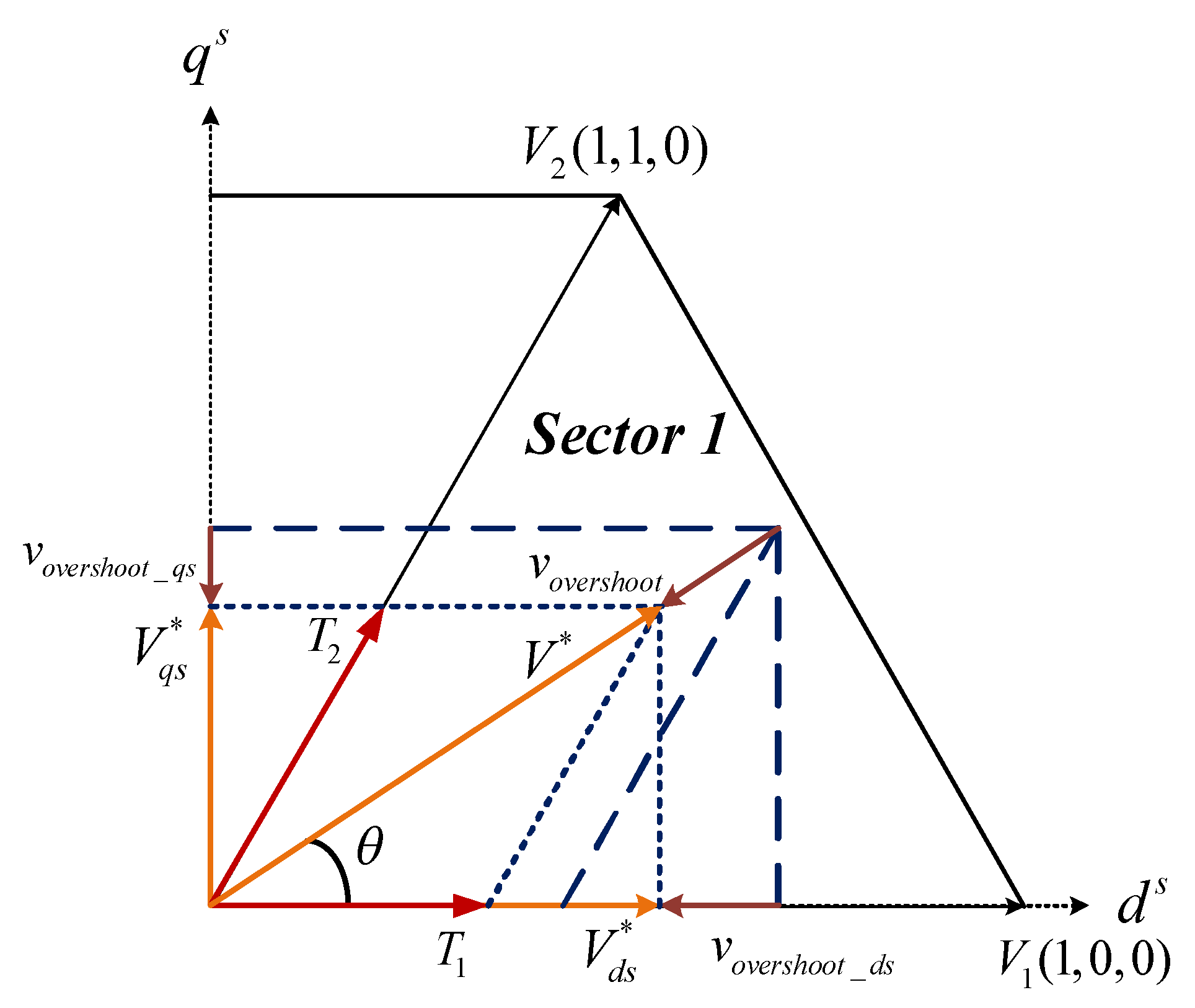
Therefore, a feedforward compensation method for changing the reference voltage is proposed, as shown in
Figure 6, without changing the carrier wave (i.e., a fixed switching frequency). The space voltage vector diagram of the proposed output voltage compensation method in
Figure 6b is illustrated, as shown in
Figure 7. It shows the case in Sector 1 (In that time,
=
). The value of
T1,
T2,
T0 is changed because the value of the reference voltage is changed by the feed forward compensation.
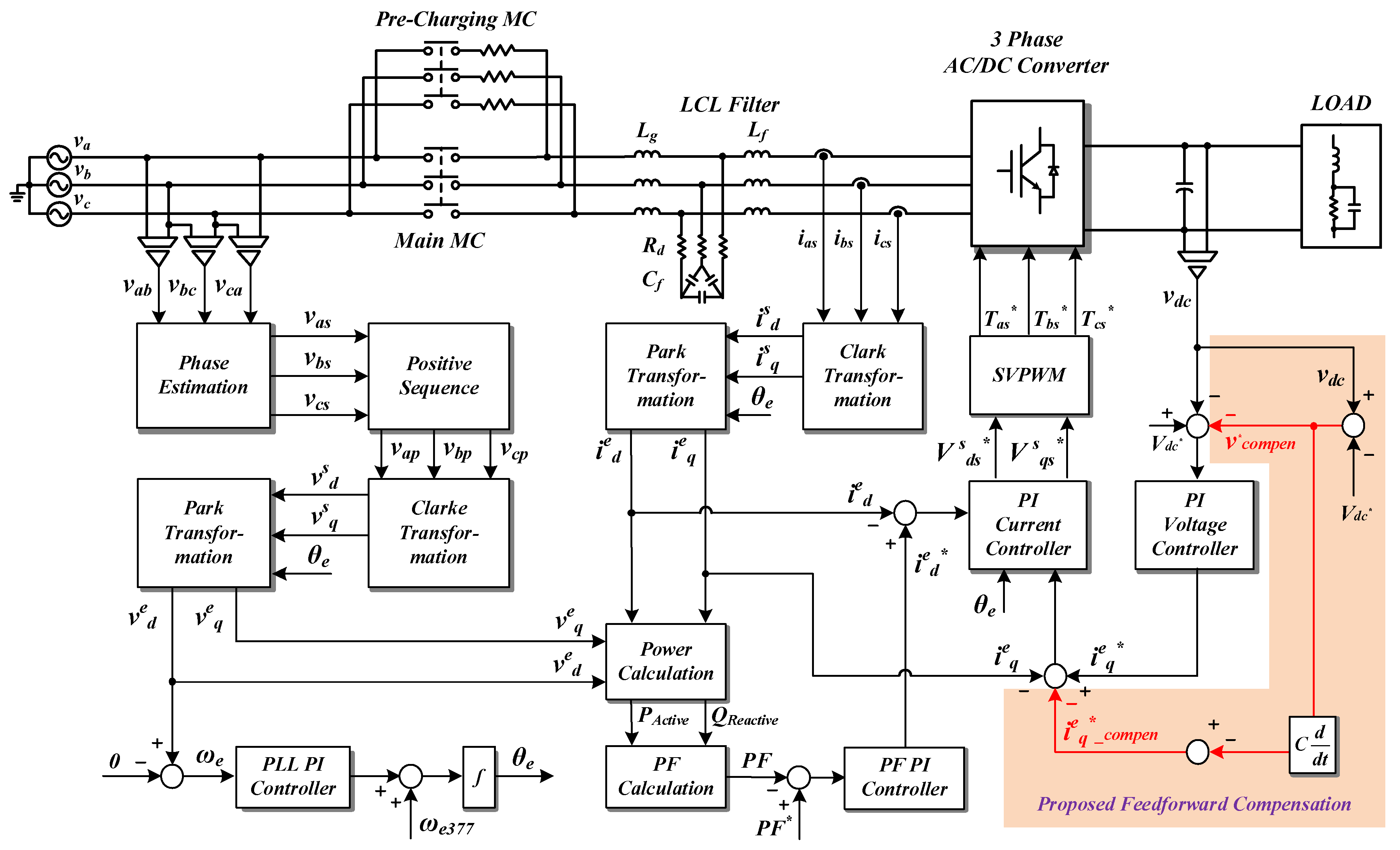
Generally, control of a three-phase inverter (or converter) generates a switching pattern using the output of the current controller. However, the proposed control method measures variations in the output voltage that it is used to compensate for the reference voltage. The compensated value is then used in the voltage controller. However, the control period of the current controller is 10 times faster than the voltage controller because of the control frequency bandwidth, and the actual switching pattern is generated using the output of the current controller. Therefore, the current controller also must perform the same compensation in order to quickly respond in the frequent transient state. The current compensation value of the current controller is obtained by the voltage variation and the capacitance of the DC-link.
Figure 8 shows the overall control block diagram of the proposed system. The voltage and the current compensation values for transient state were applied to each controller. In
Figure 8,
is voltage angular speed of AC side for VOC and phase locked loop (PLL).
is fixed value of AC grid (60 Hz).
means active current and
means reactive current.
,
are the values synchronous
d-
q transformed of input voltage.
is DC-link voltage,
is DC-link current.
and
are resistor and inductance of converter side, respectively.
4. Experimental Result
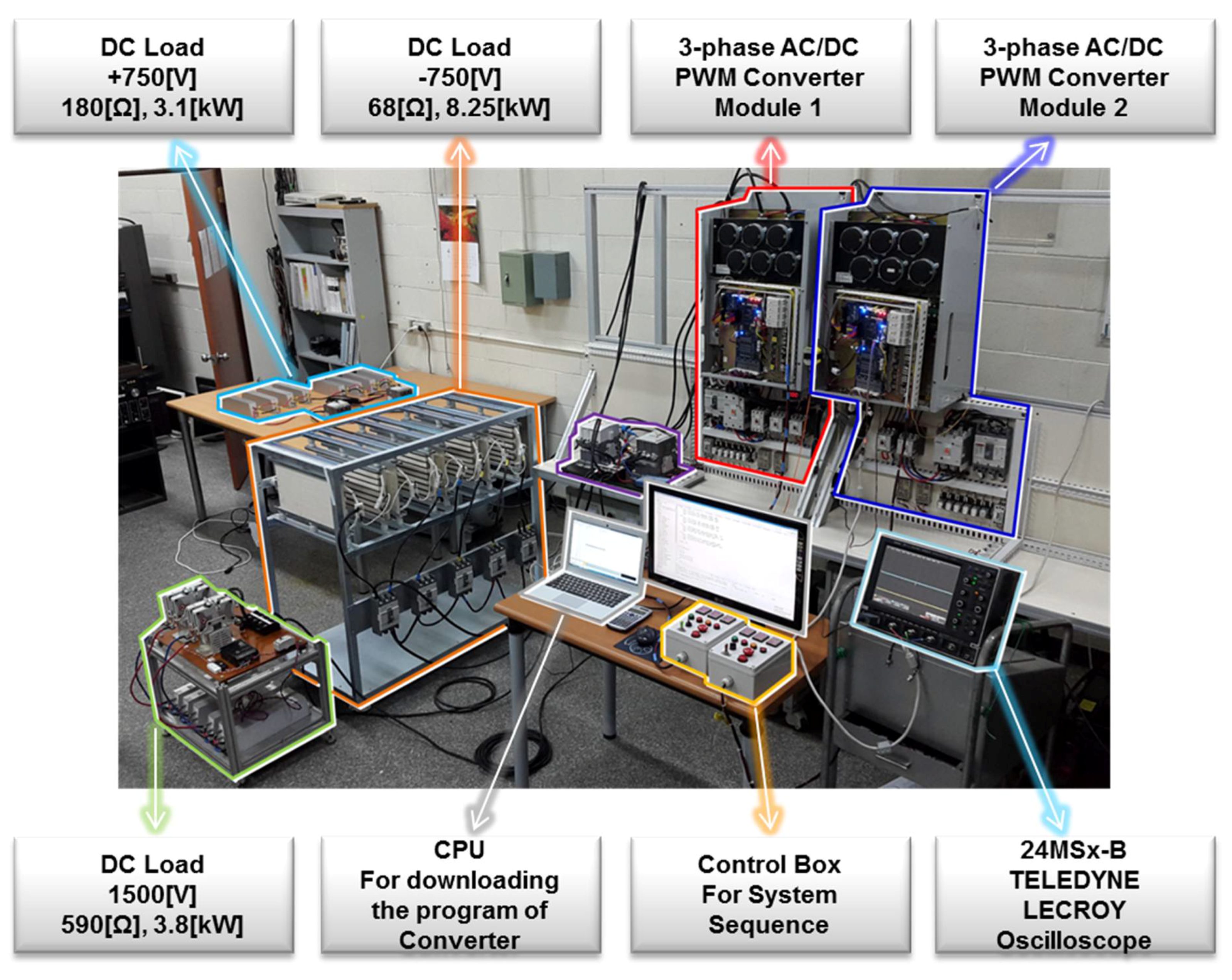
The hardware configuration for applying the proposed compensation method is as shown in
Figure 12. In this paper, two AC/DC modules are applied. The capacity of each module is 50 kW and the switching frequency is set to 5 kHz. Each module controls the output voltage to 750 V
dc. The output of each module is configured in series. Therefore, the final distribution voltage is ±750 V
dc. The loads that are connected to the proposed system can use various voltages.
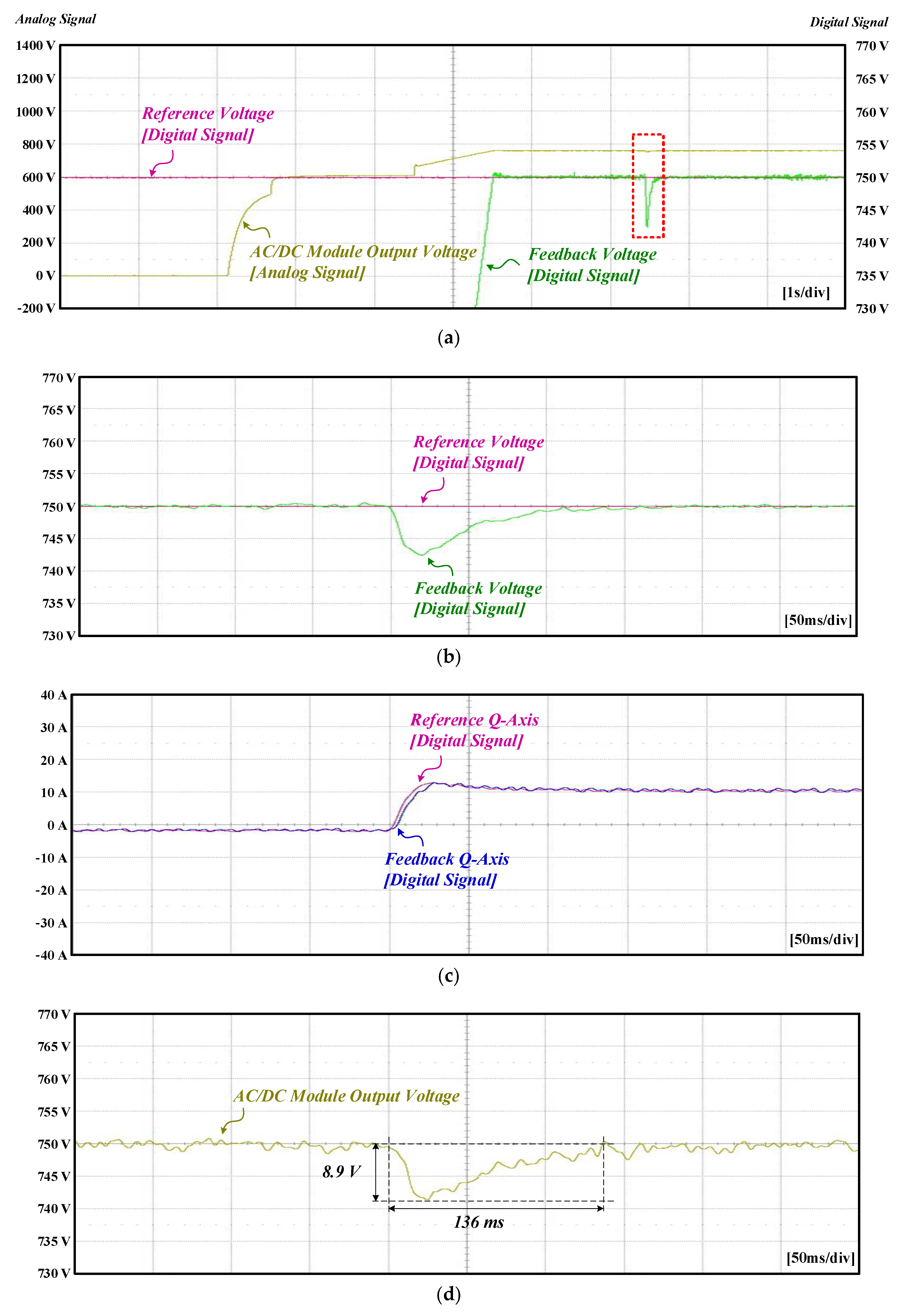
Figure 13 shows the experimental waveforms that are not applied to the proposed compensation method of 3-phase AC/DC PCS. A soft start is applied for minimizing exceed current inflow to capacitor during initial operation. 7 kW load is connected after output voltage is stable as 750 V
dc (in ±1% during 2 s).
Figure 13b shows the expanded waveform of the reference and feedback voltage of the voltage controller when the load is applied, as in
Figure 13a. The reference voltage of the voltage controller is 750 V
dc and it can be confirmed that the output voltage instantaneously decreases when the load is applied.
Figure 13c shows the waveform of the
q-axis reference and feedback of the current controller when the load is applied. At the moment of undershoot, the reference value of the current controller changes, but the output (=feedback) of the controller shows a slower response than the reference. Since the current controller and the voltage controller are operated separately and the actual switching waveform is generated using the output of the current controller, the two controllers must each be compensated for, respectively.
Figure 13d shows the expanded waveform of the output voltage of the 3-phase AC/DC PCS in
Figure 13a. When the load is applied, it can be confirmed that an undershoot of about 8.9 V occurs for 136 ms.
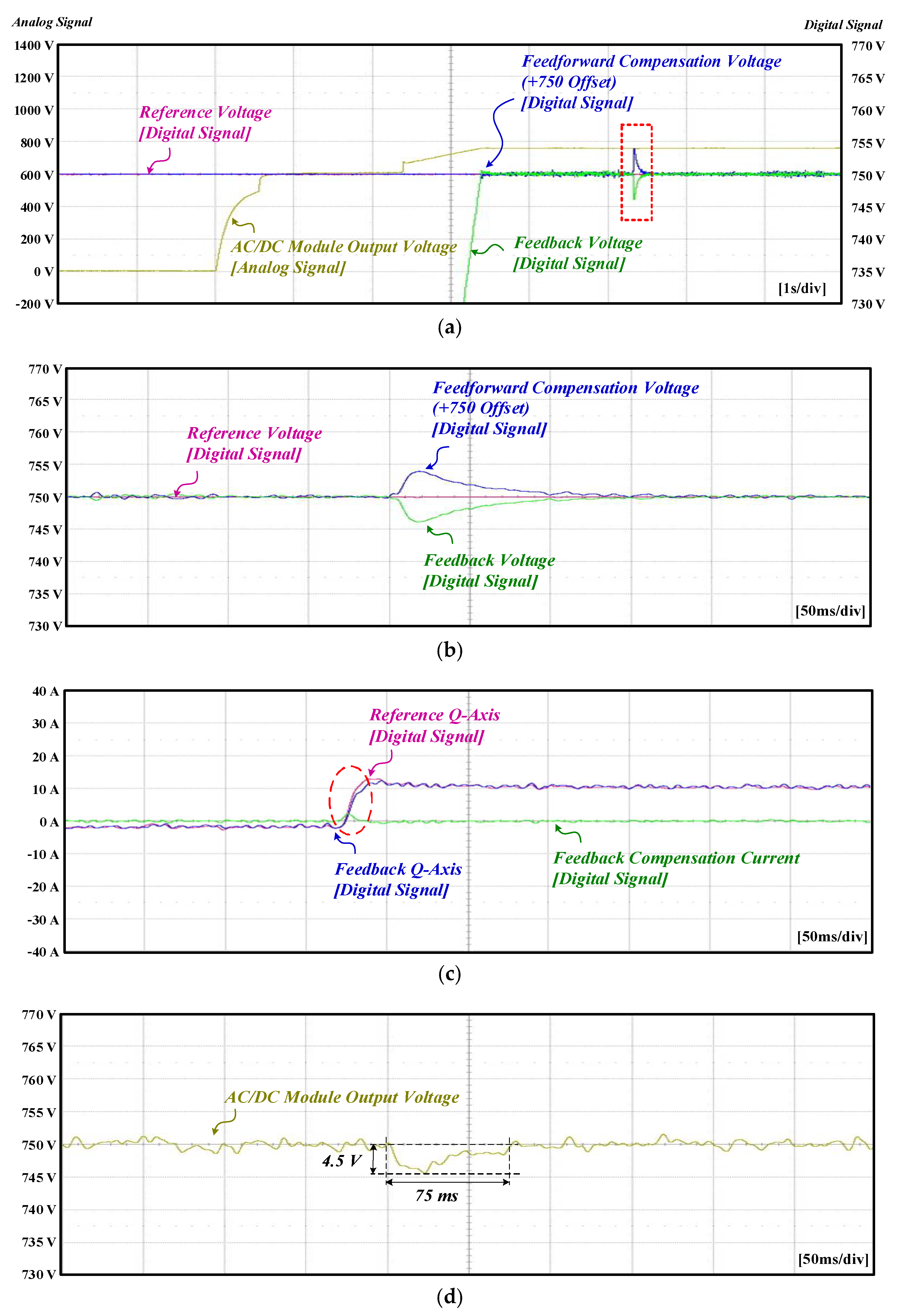
Figure 14 shows the experimental waveform of a 3-phase AC/DC PCS using the proposed output voltage feed forward compensation method. Experiments were carried out under the same conditions, as in
Figure 13.
Figure 14b shows the output of the voltage controller using the proposed compensation method when the load is applied. The undershoot is reduced when compared to that shown in
Figure 13, because the reference voltage of the voltage controller is 750 V
dc and the forward compensation value is applied when the load is applied.
Figure 14c shows the output of the current controller using the compensation method. The response characteristic is improved in the section where the voltage variation occurs by the compensation to current controller based on
Figure 8 when overshoot (or undershoot) occurs as compared to the results in
Figure 13c.
Figure 14d shows the output voltage of a three-phase AC/DC PWM converter. When the load was applied, about a 4.5 V undershoot occurred for 75 ms. When the proposed feed forward compensation method is applied, the magnitude of undershoot is reduced by 50% and the response is improved by 45%.


