A Four-Level T-Type Neutral Point Piloted Inverter for Solar Energy Applications


1
Power Electronics and Renewable Energy Research Laboratory (PEARL), Department of Electrical Engineering, University of Malaya, Kuala Lumpur 50603, Malaysia
2
Department of Electrical Engineering, Faculty of Engineering, University of Malaya, Kuala Lumpur 50603, Malaysia
*
Author to whom correspondence should be addressed.
Energies 2018, 11(6), 1546; https://doi.org/10.3390/en11061546
Submission received: 9 April 2018
/
Revised: 25 May 2018
/
Accepted: 28 May 2018
/
Published: 13 June 2018
(This article belongs to the Special Issue Power Electronics 2018)
Abstract
:Multilevel inverters provide an output signal with low harmonic distortion and superior output voltages. This work proposes a new four-level T-type neutral point piloted (T-NPP) topology with higher efficiency and low total harmonic distortion (THD) and with the ability to withstand high voltage stresses, especially for high-power applications. The proposed topology is designed in such manner that the direct current (DC)-voltage stresses split over the components with strong possibilities to increase the load current and switching frequency. However, the operation of the proposed topology is based on two essential principles. The first principle is that each upper and lower switch of each leg consists of two insulated gate bipolar transistors (IGBTs) connected in series in order to withstand high voltage stresses and make it split over the two IGBTs in each switch. The second principle is using the DC-link circuit (T1 & T2) to generate 2Vdc and 1Vdc by connecting the bidirectional switches of each leg to the DC-link’s mid-point. Furthermore, the proposed four-level T-NPP inverter outperforms other converters by the high number of output voltage level, low number of components, simple structure and higher efficiency. Finally, the proposed T-NPP topology concept was validated via simulation, experiments and theoretical analysis.
1. Introduction
Multi-level inverters are the most commonly used inverters in industrial applications and other renewable energy applications because they provide pure output voltage’s waveforms. For low power applications such as photovoltaic systems [1,2,3,4,5,6], multilevel inverters are capable to produce semi-pure output waveforms with power semiconductor s devices. The neutral-pointed converter (NPC) [7,8], flying capacitor (FC) [9,10] and cascaded H-bridge (CHB) [11] are the most common inverters and are illustrated in [12,13,14]. The issues of neutral-point voltage in NPC such as voltage deviation, the unbalanced voltage across the capacitors of the FC topologies [15], and a large number of separate direct current (DC) supplies in CHB are the main drawbacks to be considered in these topologies [16,17,18,19,20]. In addition, these topologies are not suitable for low-voltage applications since the switching and conduction losses are getting increased due to the two-series connected switches especially in two-level inverter [21]. Contrary to the NPC topology, the T-type inverter is very efficient for low switching frequencies due to its low conduction losses and the fact it needs only three additional isolated gate derives.
The T-type inverter is showing a good performance during the operations and could be an alternative choice in industrial applications since it combines the main merits of both the two-level converter, and the three-level converter, such as low power losses and high-quality waveforms for the output voltages [22].
Furthermore, T-type converters can be used for medium-voltage applications [23,24] by adding devices connected in series with the upper and lower switches in every single leg, in which special gate-derived units are needed for the voltage balancing and transient [25,26]. For medium-voltage applications, T-type inverters are known to be neutral point piloted (NPP). The bidirectional switches of such inverters replace the clamping diodes that connect the points between the capacitors and the switches. The NPP structure is aimed at a medium voltage (3.3, 6.6, and 9.9 kV) and high power of up to 48 MW [27]. Furthermore, the series connection of the upper and lower switches allows this topology to operate under high frequencies and variable high-speed applications, and this topology is known as TCC [24]. In addition, the bidirectional switches in NPP topology are used to control the current path and to generate the zero-voltage level. However, this topology can only produce three-level output voltages using the capacitors which are connected to the input DC-link voltage.
T-type converters can be used for low-voltage applications with better advantages compared to the other types of three-level topologies [28,29]. Instead of a three-level NPC topology, an active bidirectional switch is employed to the DC-link voltage midpoint, thus serving as an alternative to increasingly complex three-level topologies [30,31,32,33,34]. Although a T-type converter comprises two switches connected in series, it exhibits very low switching losses and acceptable conduction losses because the bidirectional switches block only half of the DC-link voltage.
In this paper, a T-NPP topology with less number of power components and zero-passive components such as capacitors to generate four levels of output voltages with low harmonic distortion and high efficiency is presented. The T-NPP topology is an extended version of the proposed four-level T-type topology presented in [35] which is originally proposed for low-voltage application. However, the T-NPP is proposed for high and medium voltage application and designed in such manner that the DC-voltage stresses split over the components with strong possibilities to increase the load current and switching frequency. In addition, the concept of T-NPP topology is based on the combination of the four-level T-type topology presented in [35] and separated DC-link which is designed to increase the output voltage level. In fact, the proposed topology can be used for high-power applications with less switching and conduction losses compared to the other topologies as presented in the following sections.
2. The Proposed Topology and Its Operations
The proposed T-type neutral point piloted (T-NPP) topology is designed for medium-and high-power applications based on the NPP topology which is designed to produce an output voltage with levels either 0 or ±Vdc. NPP topology is designed in such manner to be capable of bearing high-voltage stress and provide a controllable path for the current through the clamping devices. However, the proposed topology is designed to overcome the drawbacks of the NPP topology and NPC in terms of the total harmonic distortion (THD), voltage stress, and limitation in operating in high-frequency and that can be done by an appropriate design and by increasing the output voltage levels.
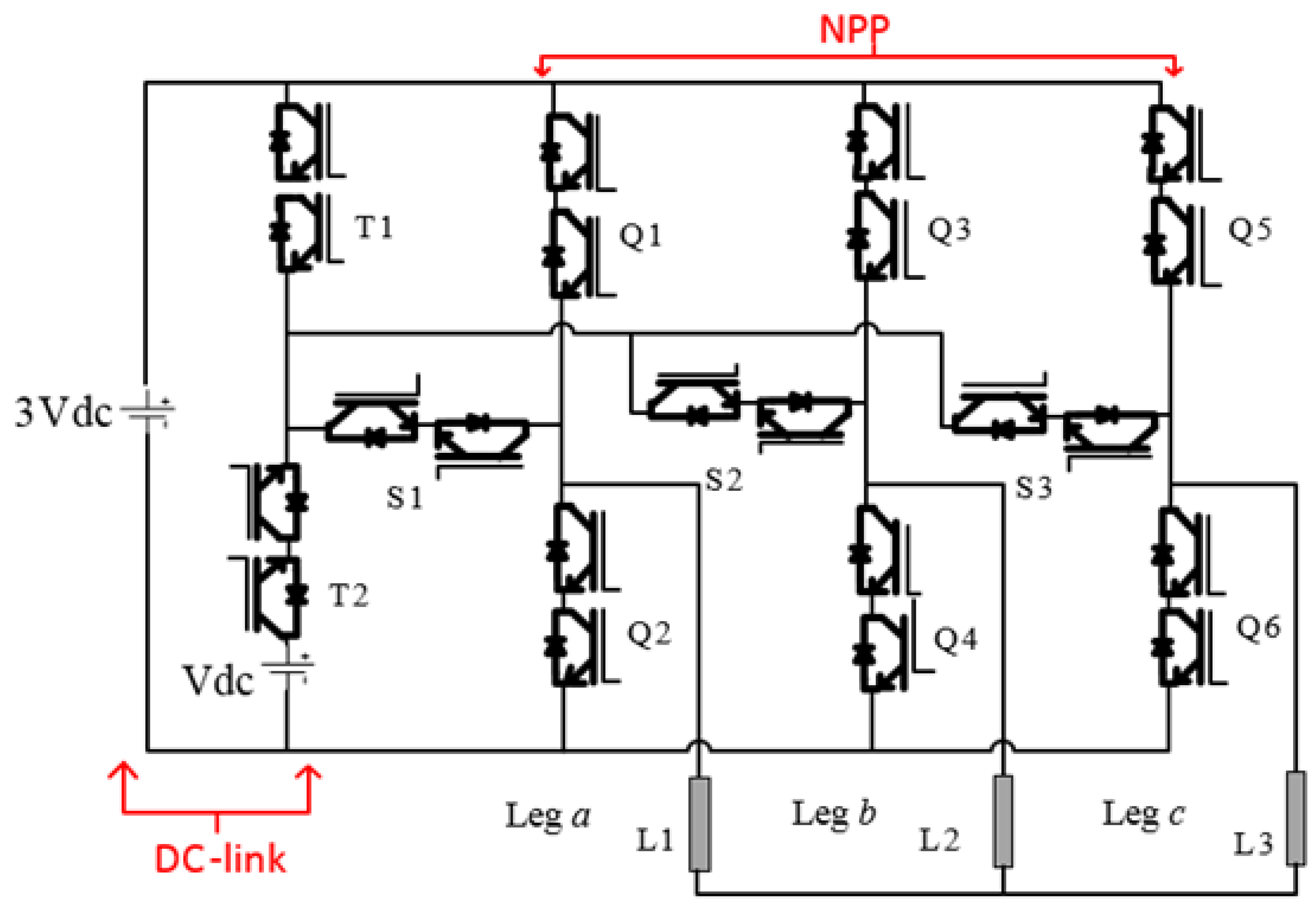
Figure 1 shows the proposed topology which consists of two parts. The first part is the NPP topology with no clamping capacitors. The second part is the DC-link circuit connected to the bidirectional switches of each leg. Furthermore, DC-link circuit consists of four switches in which every two switches are connected in series in order to reach the medium voltage and be capable of bearing high-voltage stress.
Instead of using the bidirectional switches of each leg for generating 0Vdc such as NPP or NPC, those bidirectional switches are connected directly to the mid-point of the DC-link in T-NPP in order to generate 1Vdc and 2Vdc as shown in Figure 2b,c respectively. However, the 0Vdc can be generated by the lower switches in each leg of T-NPP. Also, the 3Vdc is generated in each leg by upper switches which are connected directly to 3Vdc as it is shown in Figure 1. The switching state of the proposed topology (T-NPP) is provided in Table 1.
The bidirectional switches (T2 and T3) of the three-level T-type inverter is connected to the mid-point (0) to produce 0Vdc in each leg. In order to extend the output-voltage to N levels, we eliminate the mid-point (0) and connect the bidirectional switches of each leg to an external DC-link circuit and the voltage stress across the upper and lower switches of each leg can be reduced by replacing them with double-IGBT connected in series as it is presented in Figure 1. During the switching transitions from one voltage level to another, the current will commutate to the right path without any occurrence of a short circuit or voltage deviation and this is one of the positive aspects of the proposed topology. Figure 2 shows the current commutation during the switching transitions and switching states of the output voltage levels shown in Figure 3.
The series switches (T1 and T2) of the DC-link operate at the same time only during generating 2Vdc without any short circuit occurrence or voltage deviation and this principle was validated successfully via analytical comparison with the presented topology shown in Figure 4, and building the prototype shown in Figure 5 to obtain the simulation and experimental results in which can be clearly noticed from the waveforms of the output voltages shown in Figures 6–9.
In Figure 2b, T1 and T2 are initially set to be closed to generate 2Vdc and minimize the switching losses during the transition between voltage levels. In this case, the DC-voltages (3Vdc and Vdc) are connected in one loop circuit (−3Vdc + Vdrop-T1 + Vdrop-T2 + Vdc). By ignoring the voltage drop across the two-insulated gate bipolar transistors (IGBTs) connected in series, the difference voltage in any point (inside the dc-link circuit) between 3Vdc and Vdc will be 2Vdc (3Vdc − 1Vdc = 2Vdc).
In this case, the loop of dc-link circuit plays as dc-voltage source and inject 2Vdc to the bidirectional switches of each leg. In Figure 2a, S1 is opened so that only 3Vdc will be connected to the upper switch Q1 and generate 3Vdc. Also, In Figure 2a, the status of T1 will not be considered since the bidirectional switch (S1) is off.
Because the modularity has become one of the pillars of modern manufacturing as it speeds up assembly, repair, and manufacturing process, all the switches of the T-NPP have been adjusted to the same voltage rating which is can be either 3Vdc or more. However, the value of the voltage stresses across the switches are different from each other and that is according to the point that every switch is connected to. In other words, some of the switches are faced with high voltage stresses compared to the rest especially those are connected directly to the main voltage source (3Vdc). However, the voltage stresses split over the series connection of each switch in each leg of the proposed topology.
3. Modulation Technique
The modulation technique is one of the most feature for implementing T-NPP topology. Because of the synchronization of the switching transition of two legs, staircase and modified space-vector modulation could be used for the proposed topology. In other words, the DC-link circuit of the proposed T-NPP topology is incapable to produce 1Vdc and 2Vdc at the same time and this is one of the drawbacks of using DC-link inside T-NPP topology.
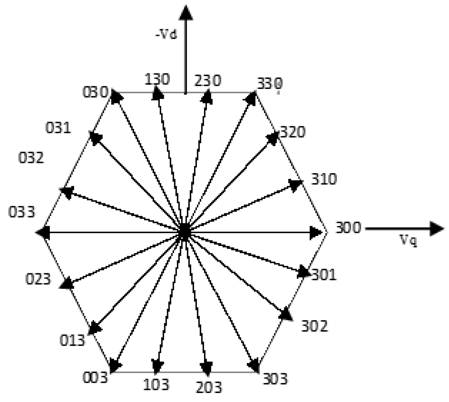
Figure 3 shows the space vector references in the d-q frame and its components, which can be found and represented by the equations below [16]:
where Vq, and Vd are the voltage components in d-q frame. Also, Sa, Sb, and Sc are the switching states of leg a, b, and c, respectively.
In addition, the switching state of the proposed topology is arranged in such manner to reduce the switching losses by decreasing the number of switching during the transitions between voltage levels according to the switching state vectors shown in Figure 3.
Table 2 shows the voltage sequences and switching states of all the switches in one period during the operation among the three legs. Based on Table 2 and Figure 3, the T1 and T2 are only changed into another switching state once generating out 1Vdc and 2Vdc. However, the output voltages (3Vdc and 0Vdc only) from each leg are independent on the switching state of T1 and T2. This modulation technique is called the modified staircase technique.
4. Losses Analysis and Comparisons
Efficiency is one of the significant features to ensure the feasibility of the proposed topology compared to the other topologies. Apparently, T-NPP topology requires less number of components compared to the other topologies such as FC, and NPC. In fact, minimizing the number of the power components used and switching devices results in the higher efficiency and less power losses.
However, T-NPP topology operates with good performance and higher efficiency and one of such a reason for that is the absence of the passive components such as clamping diodes, and FCs as well as the minimum number of DC-link supplies. Furthermore, the efficiency analysis for the T-NPP topology can be done by the following methods.
4.1. First Method
In this method, the conduction and switching losses analysis can be done by taking into account the rating of the components from the input side of the circuit up to the load side. Practically, three phase series resistive–inductive load (142 Ω–15.3 mH) in start connection is used as a load. Also, the IGBTs selected are HGTG20N60B3D, in which the maximum value of the forward current is 19 A and the direct voltage is 600 V. The data sheet provides all the curves of the energy losses, collector-emitter current, saturation voltage, and forward voltage of the diodes. Those curves are approximated by an exponential equation using the curve-fitting tool of MATLAB [36] as follow:
where the Vce is the collector-emitter voltage, Eon is the energy dissipated during the on-state, and Eoff is the energy dissipated during the off-state.
The conduction and switching losses can be calculated using the below equations:
in which i(t) is the maximum load current.
PT = PSW + Pcond
However, PLECS software (Version 4.1, Plexim , Cambridge, MA, USA) is capable to calculate the switching losses based on the recording of the semiconductor’s operating condition (forward current, blocking voltage, and junction temperature) before and after the switching operation. The data tables and equations of the switches can be inserted manually via PLECS’ integrated visual editor.
4.2. Second Method
In this method, the power losses of the proposed topology were calculated via PLECS software and presented in details in this section. The comparison of power losses between the proposed topology and four-level nested multilevel topology [18] which is shown in Figure 4 for illustration and more convenience. Furthermore, the conduction and switching losses for both proposed T-NPP topology and four-level nested configuration are validated via simulation in PLECS software and tested via experiments [18] in various types of loads and DC-link voltages.
Different values of loads were applied for the comparison of losses purpose are the same conditions that had been used and studied in [18]:
- (1)
- Case 1: 150 V, R = 65 Ω, L = 7 mH, fS = 720 Hz.
- (2)
- Case 2: 300 V, R = 142 Ω, L = 15.3 mH, fS = 720 Hz.
- (3)
- Case 3: 600 V, R = 142 Ω, L = 15.3 mH, fS = 720 Hz.
As seen from Table 3, for each case, the proposed four-level T-NPP topology has less power losses compared with the four-level nested configuration. Based on those results, the efficiency of the proposed topology is much higher because of less number of components that had been used, no extra diodes and no FCs. Furthermore, minimizing the switching time and number of turning on–off devices during the transition is one of the strategies made to reduce losses. In fact, the lack of modularity is one of the drawbacks of the proposed topology T-NPP due to the different voltage stresses across the components. However, this issue is no longer existing if all the switches used have the same voltage rating.
Additionally, 3Vdc is the maximum value of voltage stress across the components, so that in order to prevent any short circuit occurrence or voltage deviation inside the circuit, the voltage rating of the switches must be equal to 3Vdc or more.
5. Simulated and Experimental Results
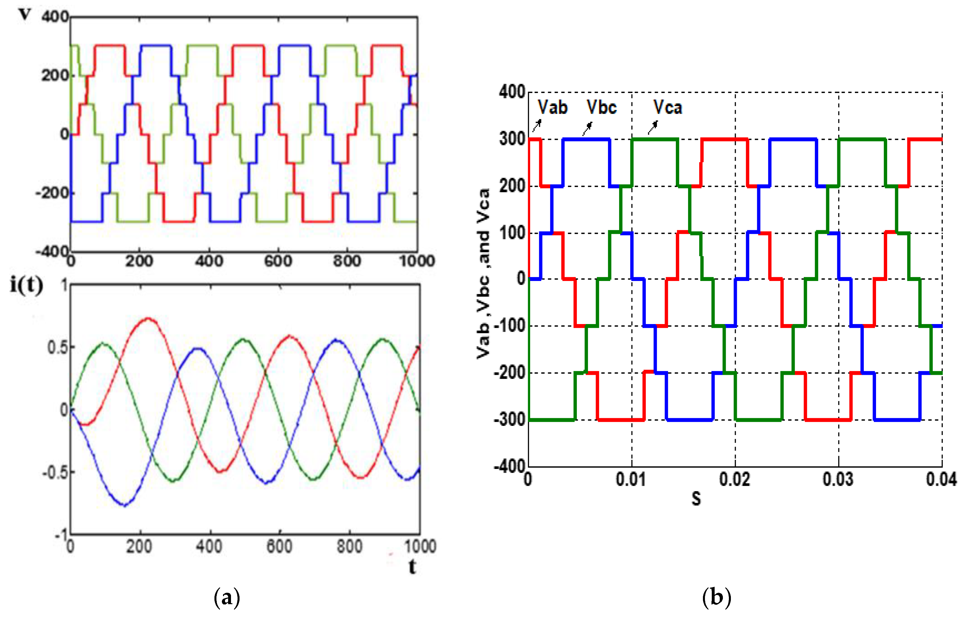
The proposed four-level topology (T-NPP) for high- and medium-power applications depicted in Figure 1 was implemented and its prototype was built as shown in Figure 5. The validity of the T-NPP was proven successfully via simulation and experiments. Furthermore, the simulation was run by MATLAB Simulink and PLECS software and the obtained results are shown clearly in Figure 6 and Figure 7. Such a result shown in Figure 6 and Figure 7 proves that the output waveforms of the T-NPP are purely generated according to the adjusted DC-link voltages and desired output voltage level.
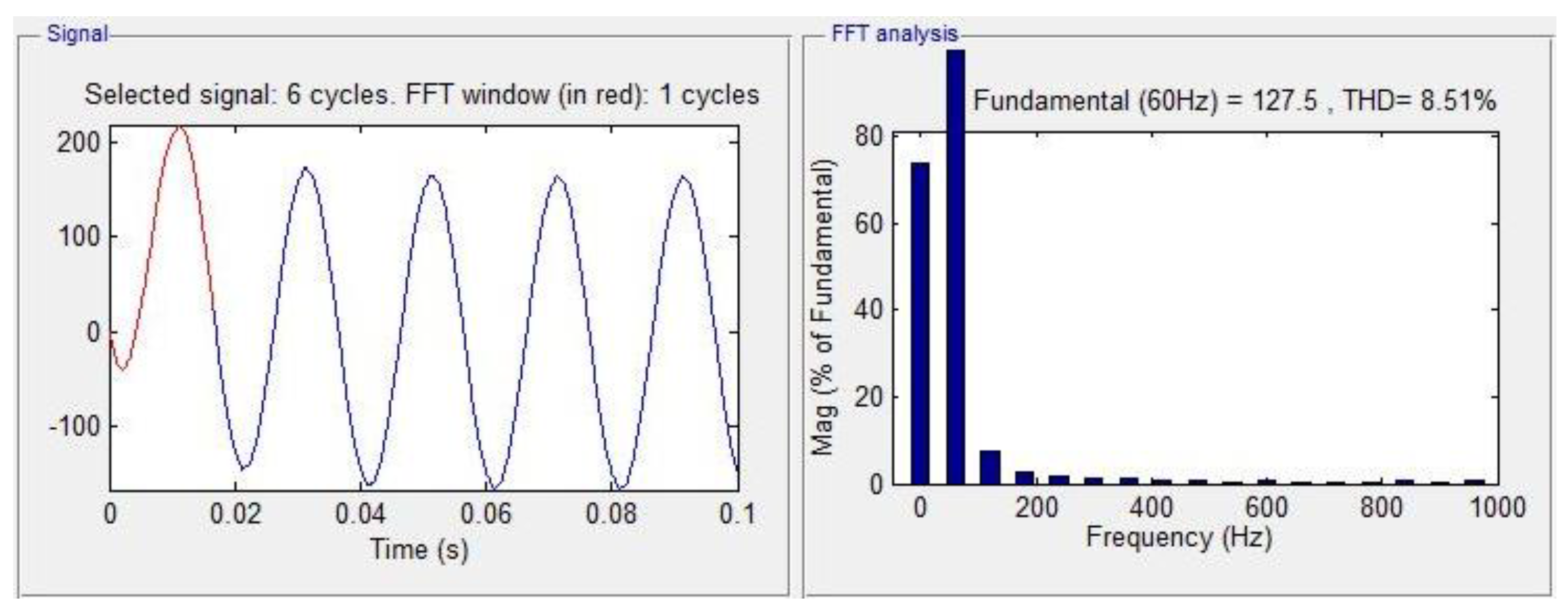
The staircase modulation technique and modified space vector modulation technique are the applicable control methods for the T-NPP for generating pure output waveforms with less switching losses. Furthermore, the THD one of the most features to measure the validity and performance of such a topology. Figure 8 depicts THD% of the current load for the proposed topology and the measured value of the THD% is 8.51% for modulation index Ma = 1.
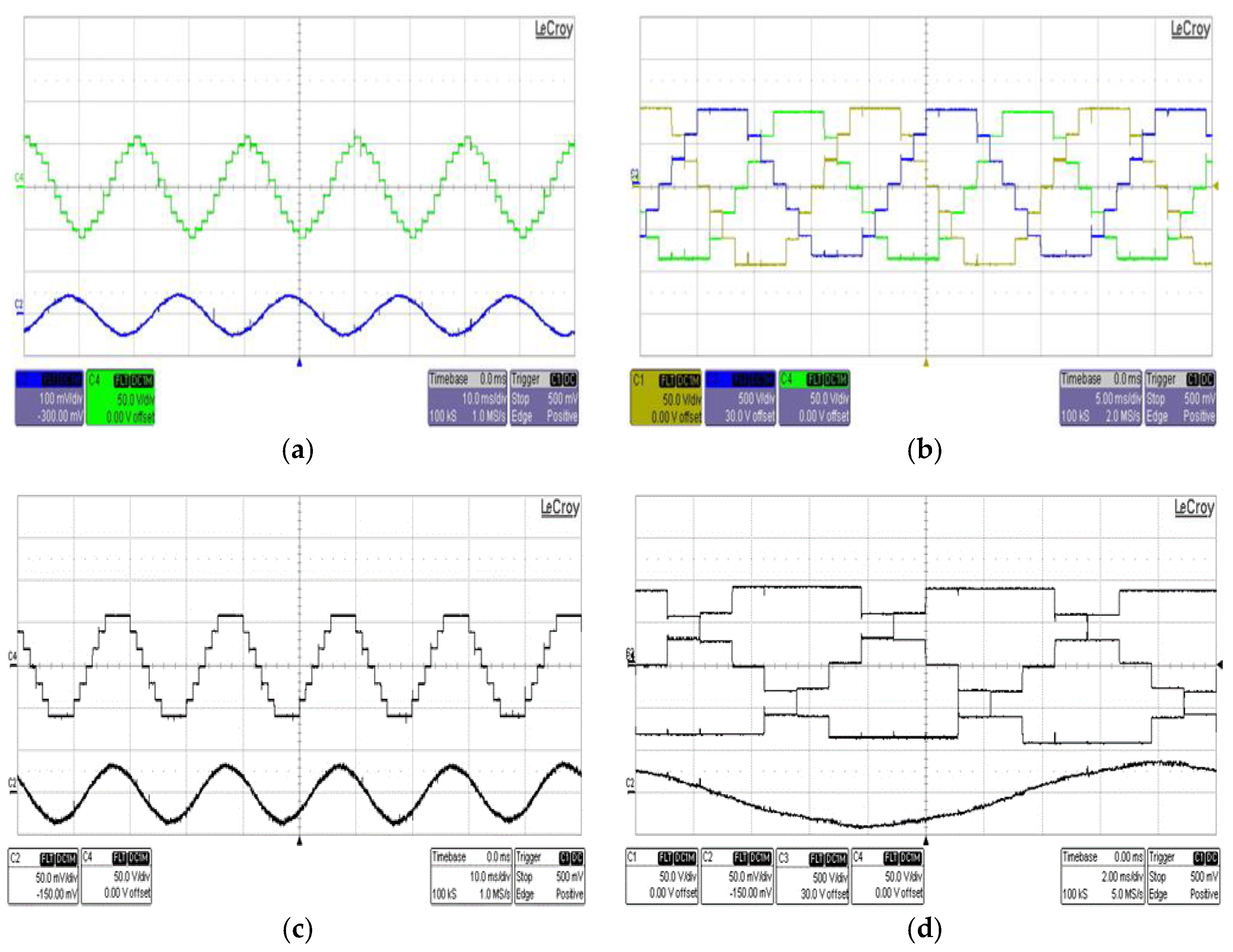
The experimental setup consists of dSPACE, gate drivers, two DC-supplies, IGBT switches, and induction motor acting as a load. Furthermore, the ratings of the components and equipment used in the experiments are shown below in Table 4. Due to the limitation of the equipment provided and for an easy implementation, the experiments were not run in low-power and low-voltage ratings. However, the feasibility of T-NPP was validated successfully via the experiments and the obtained results as shown in Figure 9.
As a result, the proposed topology combines the positive aspects of the two-level inverters such as fewer power components and advantages of the multilevel inverter such as superior output voltage and THD%. In other words, the concept of the proposed topology T-NPP is absolutely correct since it was investigated under different types of loads and conditions and all the obtained results reveal its ability to generate superior output waveforms and withstand high voltage stresses.
Table 5 shows the comparison between T-NPP and other proposed and existing topologies in terms of number of passive components such as capacitors, and the DC-link voltages. Based on Table 5, we could notice that the T-NPP has the lower number of components in which the installation area and cost, conduction and switching losses could be reduced. Furthermore, the proposed topology can be used for low-voltage power application without using two IGBTs connected in series in each upper or lower switch.
Table 6 shows the comparison between NPC, CHB, FC and T-NPP in terms of rating requirement per N-level. However, Table 7 shows the T-NPP rating requirement per level. Based on the comparison carried out, we simply notice that T-NPP outranks other topologies in terms of simplicity, performance, and cost.
The proposed topology is designed mainly for high- and medium-power applications which is presented in detail in this paper. We cannot deny that NPC is sufficient for the medium-voltage application, but T-NPP topology is constructed with two IGBTs of series connection for upper and lower switches to reduce the voltage stress across each switch.
However, the main contribution of this paper is proposing a new multilevel topology with a reduced number of components, no clamping diodes, no FCs, and higher efficiency with a sufficient control strategy to reduce the switching and conduction losses.
As it appears from the simulation and experimental results, we could conclude that the proposed topology’s concept can be a good alternative for high and medium power applications due to its good performance, simple construction and withstand higher voltages.
Based on the simulation and experimental results, we could conclude that the concept of the T-NPP is valid since the outcomes results are the same in terms of voltage-steps and current waveforms. Table 8 eshows the direct comparison between the simulation and experimental values of the parameters such as line-to-line voltages (Vab, Vbc, Vca), line-to-neutral voltage, motor load’s current and THD.
Table 8 shows the direct comparison between the outcome values of the parameters in the simulation and experiment. The output waveforms of simulation results for the line-to-line voltages (Vab, Vbc, and Vca) as shown in Figure 6 and Figure 7, are similar as the obtained experimental results one shown in Figure 9. The first three rows in Table 8 illustrate the parameters of the waveform of the line-to-line voltages such as the amplitude and voltage division in each waveform. Furthermore, the THD% of the load’s current is measured in 6 cycles in sequence and it is up to 8.51% in which the fundamental frequency for all waveforms is 60 Hz. In conclusion, we could say that the simulation results are the same as the experimental one which validates the concept of the proposed topology.
6. Conclusions
A proposed four-level T-NPP topology for low and medium-power applications has been presented. Since the proposed T-NPP topology is able to withstand high voltage ratings and the voltage stresses are split over the components of the T-NPP due to the appropriate structure and design, it could be a good alternative for high-power applications too. The proposed topology produces four-level output voltages with possibilities to increase the output load current and that resulting in decreasing the THD and bringing an advantage over the existing topologies such as NPC and NPP inverters. Based on the simulation and experimental results, we could say that the concept of the proposed topology is validated accordingly with superior output waveforms and low harmonic distortion THD% = 8.51. In contrast with the T-type inverter or NPC, the mid-point in T-NPP is connected directly to the DC-link circuit to produce 1Vdc and 2Vdc. The absence of the passive-components such as capacitors and clamping diodes, is considered one of the advantages of T-NPP since the balancing issues caused by capacitor and voltage deviation caused by clamping diodes are overcome completely. The simplicity of the proposed topology is also considered one of the merits because it enables the extension to N-level to be reached with fewer components and low cost which might be the future work. Furthermore, the modified staircase modulation technique is applied to the proposed topology to generate superior output waveforms by minimizing the number of switching times over one 1cycle with modulation index Ma = 1.
Author Contributions
S.S.A. has contributed to the theoretical approaches, simulation, experimental tests, and preparing the article; S.M. has contributed to the theoretical approaches, simulations, experimental tests, and preparing the article; H.B.M. has contributed to the theoretical approaches and preparing the article.
Acknowledgments
The authors would like to acknowledge the financial support received from the University of Malaya, Malaysia, through Frontier Research Grant No. FG007-17AFR and Innovative Technology Grant No. RP043B-17AET.
Conflicts of Interest
The authors declare no conflicts of interest.
References
- Buticchi, G.; Barater, D.; Lorenzani, E.; Concari, C.; Franceschini, G. A nine-level grid-connected converter topology for single-phase transformerless PV systems. IEEE Trans. Ind. Electron. 2014, 61, 3951–3960. [Google Scholar] [CrossRef]
- Mei, J.; Xiao, B.; Shen, K.; Tolbert, L.M.; Zheng, J.Y. Modular multilevel inverter with new modulation method and its application to photovoltaic grid-connected generator. IEEE Trans. Power Electron. 2013, 28, 5063–5073. [Google Scholar] [CrossRef]
- Krithiga, S.; Gounden, N.G.A. Power electronic configuration for the operation of PV system in combined grid-connected and stand-alone modes. IET Power Electron. 2014, 7, 640–647. [Google Scholar] [CrossRef]
- Kadir, M.N.A.; Mekhilef, S.; Ping, H.W. Dual vector control strategy for a three-stage hybrid cascaded multilevel inverter. J. Power Electron. 2010, 10, 155–164. [Google Scholar] [CrossRef]
- Mekhilef, S.; Masaoud, A. Xilinx FPGA based multilevel PWM single phase inverter. In Proceedings of the 2006 IEEE International Conference on Industrial Technology, Mumbai, India, 15–17 December 2006; pp. 259–264. [Google Scholar]
- Ahmed, M.E.; Mekhilef, S. Design and implementation of a multi level three-phase inverter with less switches and low qutput voltage distortion. J. Power Electron. 2009, 9, 593–603. [Google Scholar]
- Nabae, A.; Takahashi, I.; Akagi, H. A new neutral-point-clamped PWM inverter. IEEE Trans. Ind. Appl. 1981, IA-17, 518–523. [Google Scholar] [CrossRef]
- Boora, A.A.; Nami, A.; Zare, F.; Ghosh, A.; Blaabjerg, F. Voltage-sharing converter to supply single-phase asymmetrical four-level diode-clamped inverter with high power factor loads. IEEE Trans. Power Electron. 2010, 25, 2507–2520. [Google Scholar] [CrossRef]
- Ghias, A.M.; Pou, J.; Agelidis, V.G.; Ciobotaru, M. Initial capacitor charging in grid-connected flying capacitor multilevel converters. IEEE Trans. Power Electron. 2014, 29, 3245–3249. [Google Scholar] [CrossRef]
- Salinas, F.; González, M.A.; Escalante, M.F. Voltage balancing scheme for flying capacitor multilevel converters. IET Power Electron. 2013, 6, 835–842. [Google Scholar] [CrossRef]
- Roberge, V.; Tarbouchi, M.; Okou, F. Strategies to accelerate harmonic minimization in multilevel inverters using a parallel genetic algorithm on graphical processing unit. IEEE Trans. Power Electron. 2014, 29, 5087–5090. [Google Scholar] [CrossRef]
- Chan, P.K.; Chung, H.S.-H.; Hui, S. A generalized theory of boundary control for a single-phase multilevel inverter using second-order switching surface. IEEE Trans. Power Electron. 2009, 24, 2298–2313. [Google Scholar] [CrossRef]
- Merlin, M.M.C.; Green, T.C.; Mitcheson, P.D.; Trainer, D.R.; Critchley, R.; Crookes, W.; Hassan, F. The alternate arm converter: A new hybrid multilevel converter with dc-fault blocking capability. IEEE Trans. Power Deliv. 2014, 29, 310–317. [Google Scholar] [CrossRef] [Green Version]
- Gao, C.; Jiang, X.; Li, Y.; Chen, Z.; Liu, J. A DC-link voltage self-balance method for a diode-clamped modular multilevel converter with minimum number of voltage sensors. IEEE Trans. Power Electron. 2013, 28, 2125–2139. [Google Scholar] [CrossRef]
- Masaoud, A.; Ping, H.W.; Mekhilef, S.; Taallah, A. Novel configuration for multilevel DC-link three-phase five-level inverter. IET Power Electron. 2014, 7, 3052–3061. [Google Scholar] [CrossRef]
- Masaoud, A.; Ping, H.W.; Mekhilef, S.; Taallah, A.; Belkamel, H. Design and Implementation of a new multilevel DC-Link three-phase inverter. J. Power Electron. 2014, 14, 292–301. [Google Scholar] [CrossRef]
- De Cacau, R.G.; Torrico-Bascopé, R.P.; Neto, J.A.F.; Torrico-Bascopé, G.V. Five-Level T-Type Inverter Based on Multistate Switching Cell. IEEE Trans. Ind. Appl. 2014, 50, 3857–3866. [Google Scholar] [CrossRef]
- De Santos, E.C.; Muniz, J.H.G.; da Silva, E.R.C.; Jacobina, C.B. Nested multilevel topologies. IEEE Trans. Power Electron. 2015, 30, 4058–4068. [Google Scholar] [CrossRef]
- Menshawi, M.K.; Kadir, M.N.A.; Mekhilef, S. Voltage vector approximation control of multistage—Multilevel inverter using simplified logic implementation. IEEE Trans. Ind. Inform. 2013, 9, 2052–2062. [Google Scholar] [CrossRef]
- Masaoud, A.; Ping, H.W.; Mekhilef, S.; Taallah, A.S. New three-phase multilevel inverter with reduced number of power electronic components. IEEE Trans. Power Electron. 2014, 29, 6018–6029. [Google Scholar] [CrossRef]
- Shin, S.-M.; Ahn, J.-H.; Lee, B.-K. Maximum Efficiency Operation of Three-Level T-type Inverter for Low-Voltage and Low-Power Home Appliances. J. Electr. Eng. Technol. 2015, 10, 586–594. [Google Scholar] [CrossRef] [Green Version]
- Schweizer, M.; Kolar, J.W. Design and implementation of a highly efficient three-level T-type converter for low-voltage applications. IEEE Trans. Power Electron. 2013, 28, 899–907. [Google Scholar] [CrossRef]
- Peron-Guennegues, V.; Conilh, C.; Leclere, L. A converter topology for high current density drive applications. In Proceedings of the 14th European Conference on Power Electronics and Applications, Birmingham, UK, 30 August–1 September 2011; pp. 1–8. [Google Scholar]
- Kouro, S.; Malinowski, M.; Gopakumar, K.; Pou, J.; Franquelo, L.G.; Wu, B.; Rodriguez, J.; Perez, M.A.; Leon, J.I. Recent advances and industrial applications of multilevel converters. IEEE Trans. Ind. Electron. 2010, 57, 2553–2580. [Google Scholar] [CrossRef]
- Baraia, I.; Barrena, J.A.; Abad, G.; Segade, J.M.C.; Iraola, U. An experimentally verified active gate control method for the series connection of IGBT/diodes. IEEE Trans. Power Electron. 2012, 27, 1025–1038. [Google Scholar] [CrossRef]
- Withanage, R.; Shammas, N. Series connection of insulated gate bipolar transistors (IGBTs). IEEE Trans. Power Electron. 2012, 27, 2204–2212. [Google Scholar] [CrossRef]
- Umashankar, S.; Reddy, R. NPP Inverter Topology for Renewable Energy Applications. J. Electr. Comput. Eng. 2013, 1, 31–38. [Google Scholar]
- Joetten, R.; Gekeler, M.; Eibel, J. AC drive with three-level voltage source inverter and high dynamic performance microprocessor control. In Proceedings of the 1st European Conference on Power Electronics and Applications, Brussels, Belgium, October 1985; Volume 85. [Google Scholar]
- Takeshita, T.; Matsui, N. PWM control and input characteristics of three-phase multi-level AC/DC converter. In Proceedings of the 23rd Annual IEEE Power Electronics Specialists Conference, Toledo, Spain, 29 June–3 July 1992; pp. 175–180. [Google Scholar]
- Brückner, T.; Bernet, S.; Güldner, H. The active NPC converter and its loss-balancing control. IEEE Trans. Ind. Electron. 2005, 52, 855–868. [Google Scholar] [CrossRef]
- Leredde, A.; Gateau, G.; Floricau, D. New three level topology with shared components: Properties, losses, and control strategy. In Proceedings of the 35th Annual Conference of IEEE Industrial Electronics, Porto, Portugal, 3–5 November 2009; pp. 676–681. [Google Scholar]
- Li, J.; Liu, J.; Boroyevich, D.; Mattavelli, P.; Xue, Y. Three-level active neutral-point-clamped zero-current-transition converter for sustainable energy systems. IEEE Trans. Power Electron. 2011, 26, 3680–3693. [Google Scholar] [CrossRef]
- Ewanchuk, J.; Salmon, J.; Knight, A.M. Performance of a high-speed motor drive system using a novel multilevel inverter topology. IEEE Trans. Ind. Appl. 2009, 45, 1706–1714. [Google Scholar] [CrossRef]
- Xiao, H.; Xie, S. Transformerless split-inductor neutral point clamped three-level PV grid-connected inverter. IEEE Trans. Power Electron. 2012, 27, 1799–1808. [Google Scholar] [CrossRef]
- Alnamer, S.S.; Mekhilef, S.; Mokhlis, H. Proposed new N-multilevel family of topologies for T-type inverter. IEICE Electron. Express 2017, 14, 20170342. [Google Scholar] [CrossRef]
- Govindaraju, C.; Baskaran, K. Efficient sequential switching hybrid-modulation techniques for cascaded multilevel inverters. IEEE Trans. Power Electron. 2011, 26, 1639–1648. [Google Scholar] [CrossRef]
- Peng, F.Z. A generalized multilevel inverter topology with self voltage balancing. IEEE Trans. Ind. Appl. 2001, 37, 611–618. [Google Scholar] [CrossRef]
Figure 1.
The proposed four-level T-type neutral point piloted (T-NPP) topology.

Figure 2.
Current commutation during switching transition for positive output current to generate: (a) 3Vdc; (b) 2Vdc; (c) 1Vdc; and (d) 0Vdc.
Figure 2.
Current commutation during switching transition for positive output current to generate: (a) 3Vdc; (b) 2Vdc; (c) 1Vdc; and (d) 0Vdc.
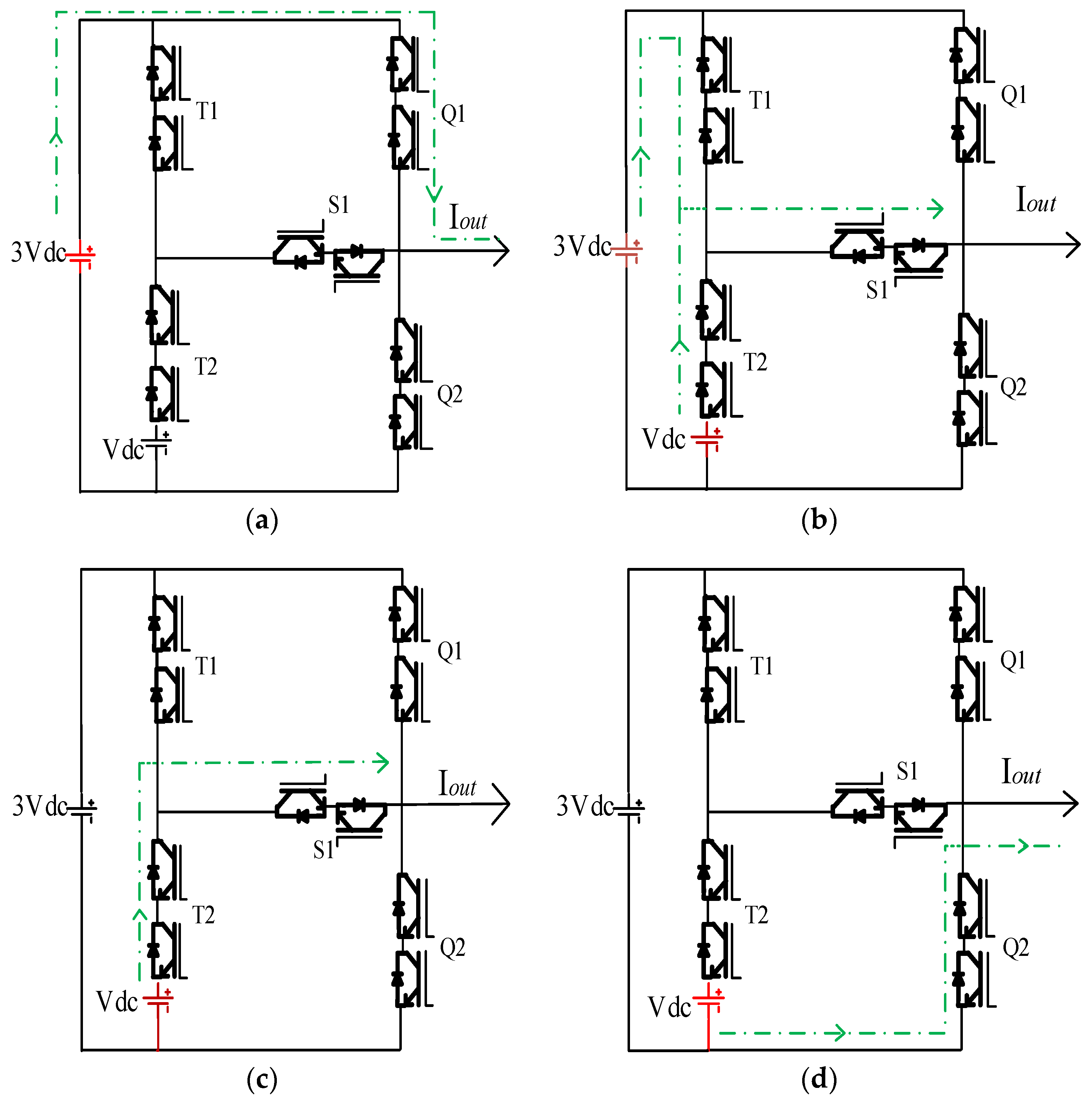

Figure 4.
Nested multilevel configuration with four level [18].
Figure 4.
Nested multilevel configuration with four level [18].
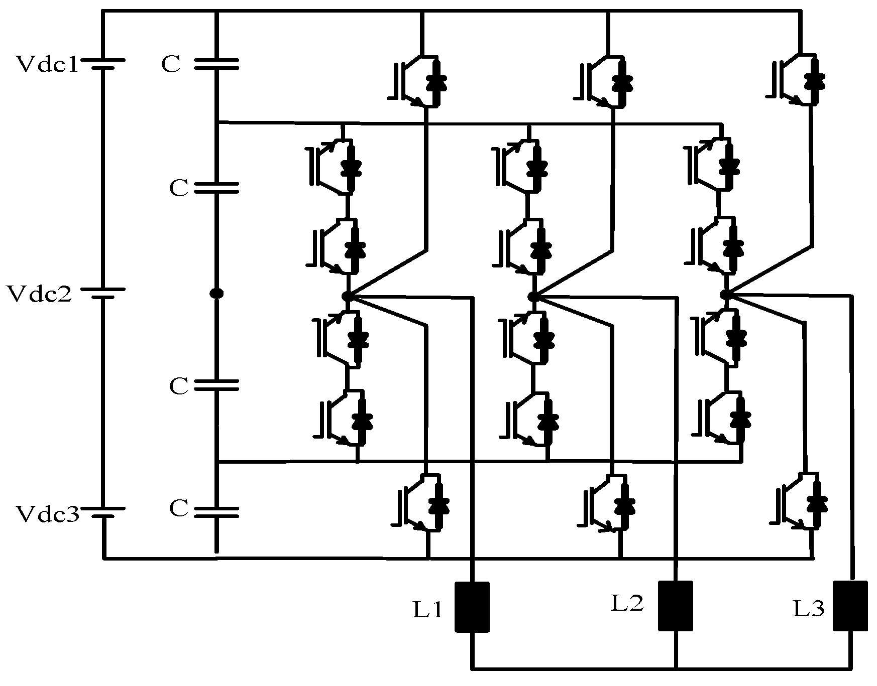
Figure 5.
The experimental setup photo.
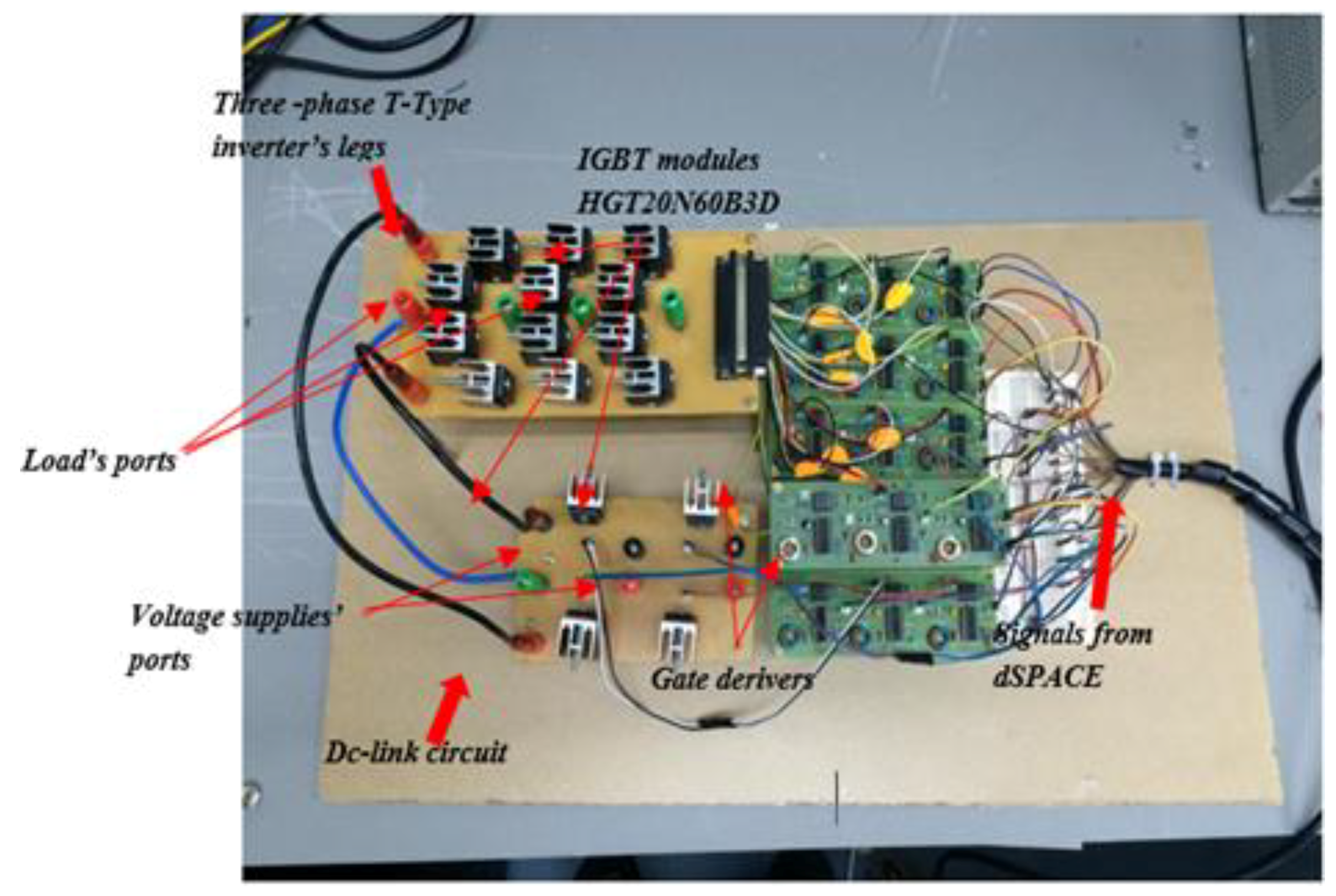
Figure 6.
Simulated results for T-NPP. (a) From top to bottom: line-to-line voltages and current of the three-phase load. (b) Staircase waveforms for the inverter line to line voltages Vab, Vbc, and Vca.
Figure 6.
Simulated results for T-NPP. (a) From top to bottom: line-to-line voltages and current of the three-phase load. (b) Staircase waveforms for the inverter line to line voltages Vab, Vbc, and Vca.

Figure 7.
Simulated results for T-NPP. From top to bottom: output line voltage, the line to neutral voltage, and line to ground voltage.
Figure 7.
Simulated results for T-NPP. From top to bottom: output line voltage, the line to neutral voltage, and line to ground voltage.

Figure 8.
The total harmonic distortion (THD) of the load’s current.

Figure 9.
Experimental results for T-NPP. (a) Line to neutral voltage and current of the induction motor load. (b) Line-to-line voltages of the induction motor load. (c) Line-to-line voltage of leg a and load’s current. (d) Line-to-line voltages and induction motor load’s current.
Figure 9.
Experimental results for T-NPP. (a) Line to neutral voltage and current of the induction motor load. (b) Line-to-line voltages of the induction motor load. (c) Line-to-line voltage of leg a and load’s current. (d) Line-to-line voltages and induction motor load’s current.


Table 1.
Switching state for the proposed topology for leg a.
| Sa | Q1 | S1 | Q2 | T1 | T2 | Van |
|---|---|---|---|---|---|---|
| 3 | 1 | 0 | 0 | 1 | 1 | +3Vdc |
| 2 | 0 | 1 | 0 | 1 | 1 | +2Vdc |
| 1 | 0 | 1 | 0 | 0 | 1 | +1Vdc |
| 0 | 0 | 0 | 1 | 0 | 0 | 0 |
Table 2.
Switching sequences for all switches of T-NPP inverter.
| Sa Sb Sc | Q1 | S1 | Q2 | Q3 | S2 | Q4 | Q5 | S3 | Q6 | T1 | T2 |
|---|---|---|---|---|---|---|---|---|---|---|---|
| 300 | 1 | 0 | 0 | 0 | 0 | 1 | 0 | 0 | 1 | 1 | 1 |
| 310 | 1 | 0 | 0 | 0 | 1 | 0 | 0 | 0 | 1 | 0 | 1 |
| 320 | 1 | 0 | 0 | 0 | 1 | 0 | 0 | 0 | 1 | 1 | 1 |
| 330 | 1 | 0 | 0 | 1 | 0 | 0 | 0 | 0 | 1 | 1 | 1 |
| 230 | 0 | 1 | 0 | 1 | 0 | 0 | 0 | 0 | 1 | 1 | 1 |
| 130 | 0 | 1 | 0 | 1 | 0 | 0 | 0 | 0 | 1 | 0 | 1 |
| 030 | 0 | 0 | 1 | 1 | 0 | 0 | 0 | 0 | 1 | 0 | 1 |
| 031 | 0 | 0 | 1 | 1 | 0 | 0 | 0 | 1 | 0 | 0 | 1 |
| 032 | 0 | 0 | 1 | 1 | 0 | 0 | 0 | 1 | 0 | 1 | 1 |
| 033 | 0 | 0 | 1 | 1 | 0 | 0 | 1 | 0 | 0 | 1 | 1 |
| 023 | 0 | 0 | 1 | 0 | 1 | 0 | 1 | 0 | 0 | 1 | 1 |
| 013 | 0 | 0 | 1 | 0 | 1 | 0 | 1 | 0 | 0 | 0 | 1 |
| 003 | 0 | 0 | 1 | 0 | 0 | 1 | 1 | 0 | 0 | 0 | 1 |
| 103 | 0 | 1 | 0 | 0 | 0 | 1 | 1 | 0 | 0 | 0 | 1 |
| 203 | 0 | 1 | 0 | 0 | 0 | 1 | 1 | 0 | 0 | 1 | 1 |
| 303 | 1 | 0 | 0 | 0 | 0 | 1 | 1 | 0 | 0 | 1 | 1 |
| 302 | 1 | 0 | 0 | 0 | 0 | 1 | 0 | 1 | 0 | 1 | 1 |
| 301 | 1 | 0 | 0 | 0 | 0 | 1 | 0 | 1 | 0 | 0 | 1 |
Table 3.
Comparison of losses for newly proposed topology and nested topology for the four-level configuration.
Table 3.
Comparison of losses for newly proposed topology and nested topology for the four-level configuration.
| Proposed Four-Level Configuration | Four-Level Nested Topology [18] Figure 4 | |||||
|---|---|---|---|---|---|---|
| Case | SW | Cond | Total (W) | SW | Cond | Total (W) |
| 1 | 0.078 | 0.75 | 0.828 | 0.26 | 2.58 | 2.84 |
| 2 | 0.067 | 1.37 | 1.437 | 0.56 | 2.41 | 2.91 |
| 3 | 0.265 | 1.88 | 2.145 | 1.07 | 2.5 | 3.57 |
Table 4.
Rating of the setup experiment components and equipment.
| Item | Rating |
|---|---|
| dSPACE | CP1104 |
| Gate driver | 5 V input–15 V output |
| DC-supply | Max 1200 V |
| IGBT | HGT20N60B3D, 19 A, max 600 V |
| Motor (load) | 400 V, 0.81 A, 0.3 kW, 50 Hz, 2800 min−1 |
Table 5.
Comparison between the proposed T-NPP and other topologies.
| Converter Type | [16] NPC | [16] | [37] | [18] | TNPP |
|---|---|---|---|---|---|
| Switches | 18 | 16 | 36 | 18 | 22 |
| Extra Diodes | 18 | 16 | 12 | 6 | 0 |
| Clamping diodes | 12 | 0 | 0 | 0 | 0 |
| DC-Supplies | 3 | 2 | 9 | 3 | 2 |
| Capacitors | No | No | Yes | Yes | No |
| No.of Levels | 4 | 4 | 4 | 4 | 4 |
| Switches voltage rating | Vdc | 3Vdc | Vdc | (0.75–)Vdc | (N − 1)Vdc |
Table 6.
Comparison between NPC, CHB, FC and T-NPP in terms of rating requirement per level n.
| Converter Type | NPC | FC | CHB | T-NPP |
|---|---|---|---|---|
| Switches voltage rating | Vdc | Vdc | Vdc | (N − 1) Vdc |
| Clamping dioeds voltage rating | Vdc | 0 | 0 | 0 |
| Clamping capacitor voltage rating | 0 | Vdc | 0 | 0 |
Table 7.
T-NPP rating requirement per level N.
| T-NPP | Main Bridge Switches | Bidirectional Switches | DC Link Switches |
|---|---|---|---|
| Switches | Q1Q6 | S1–S3 | T1T2 |
| Voltage ratings | (N − 1)Vdc | (N − 2)Vdc | (N − 1)Vdc |
Table 8.
Direct comparison between the outcome values of parameters in simulation and experiment.
| Parameters | Simulation Results | Experimental Results |
|---|---|---|
| Vab | ±300 Vp max, 100 V-step. Figure 6b | 50 V/div, 0.00 offset. Figure 9b |
| Vbc | ±300 Vp max, 100 V-step. Figure 6 and Figure 7 | 500 V/div, 30.00 offset. Figure 9 |
| Vca | ±300 Vp max, 100 V-step. Figure 6 | 50 V/div, 0.00 offset Figure 9 |
| THD% | Frequency (60) = 127.5, THD = 8.51% | Freq (60) = 127.5, THD = 8.51% |
| Line to neutral-voltage | ±200 Vp max, 100 V-step, Figure 7 | 50 V/div, 0.00 offset, Figure 9a |
| Load current | ±0.5-amp max, 0.04 s/cycle, Figure 6 | 100 V/div, −300.00 mV, 10.0 ms/div, Chanel 2, Figure 9a |
© 2018 by the authors. Licensee MDPI, Basel, Switzerland. This article is an open access article distributed under the terms and conditions of the Creative Commons Attribution (CC BY) license (http://creativecommons.org/licenses/by/4.0/).
Share and Cite
MDPI and ACS Style
Shueai Alnamer, S.; Mekhilef, S.; Bin Mokhlis, H. A Four-Level T-Type Neutral Point Piloted Inverter for Solar Energy Applications. Energies 2018, 11, 1546. https://doi.org/10.3390/en11061546
AMA Style
Shueai Alnamer S, Mekhilef S, Bin Mokhlis H. A Four-Level T-Type Neutral Point Piloted Inverter for Solar Energy Applications. Energies. 2018; 11(6):1546. https://doi.org/10.3390/en11061546
Chicago/Turabian StyleShueai Alnamer, Saddam, Saad Mekhilef, and Hazlie Bin Mokhlis. 2018. "A Four-Level T-Type Neutral Point Piloted Inverter for Solar Energy Applications" Energies 11, no. 6: 1546. https://doi.org/10.3390/en11061546
Note that from the first issue of 2016, this journal uses article numbers instead of page numbers. See further details here.