An Improved Centralized Control Structure for Compensation of Voltage Distortions in Inverter-Based Microgrids

Department of Electrical Engineering, Lorestan University, Khoramabad P. O. Box 465, Iran
*
Author to whom correspondence should be addressed.
Energies 2018, 11(7), 1862; https://doi.org/10.3390/en11071862
Submission received: 13 June 2018
/
Revised: 10 July 2018
/
Accepted: 12 July 2018
/
Published: 17 July 2018
(This article belongs to the Section F: Electrical Engineering)
Abstract
:Recently, increased use of non-linear loads has intensified the harmonic distortion and voltage unbalance in distribution systems. Inverter Based Distributed Generators (IBDGs) can be employed as distributed compensators to improve the power quality, as well as to supply distribution systems. In this paper, an enhanced hierarchical control scheme for the compensation of voltage disturbance in an AC Micro Grid (MG) that includes of two control levels is proposed. The secondary control level is performed by a centralized controller. Data of voltage harmonics and voltage unbalance at the MG Sensitive Load Bus (SLB) is sent to the centralized controller by a measurement unit. A general case with a combined voltage harmonic and unbalance distortion is considered. The compensation coefficients for IBDG units are computed by the centralized controller, and reference commands are sent to the local controllers of the IBDG units that act as a primary level of control. In the secondary control level, harmonic analysis is performed for the MG in order to provide a guide for properly assigning the harmonics and unbalance compensation priorities to IBDGs at different locations in the distribution system. Some buses have more participation in exciting the MG resonance modes; therefore, larger harmonic compensation factors are considered for the IBDGs that are near to these buses. For other IBDGs, the voltage unbalance compensation factor is selected bigger. The control system of the IBDGs mainly includes a current controller, a virtual damping resistor loop, and a load compensation block. Effectiveness of the proposed control scheme is demonstrated through simulation studies.
1. Introduction
The proliferation of nonlinear loads and power electronic equipment has caused high penetration of harmonic pollution and voltage unbalance in electrical systems [1]. This might result in malfunction or overheating in devices and motors. Identifying and damping these distortions in the network help to improve voltage and power quality. On the other hand, Distributed Generators (DGs) units are increasingly being implemented in the network; they usually connect via an interface inverter. The inverter in the output stage of the DG is able to control output power, voltage, or current. However, recently some control approaches are proposed to control the inverter to compensate for power quality problems [2,3,4,5,6,7]. Most of these methods use the extra capacity of the inverters. For example in [2], each DG unit of MG is controlled as a negative sequence conductance to compensate for voltage unbalance. In this approach, which is implemented in the synchronous dq reference frame, compensation is done by generating a reference for negative-sequence conductance based on the negative-sequence reactive power. Then, this conductance is applied to produce the compensation reference current. An autonomous voltage unbalance compensation scheme which works based on the local measurements is proposed in [3] for DGs of an islanded MG. By applying this method, DGs voltages become balanced despite the presence of unbalanced loads. However, under severely unbalanced conditions, a large amount of the interface converter capacity is used for compensation, and it may interfere with the active and reactive power supply by the DG. In [4,5,6,7], the inverters emulate a resistance at harmonic frequencies to compensate for voltage harmonic distortion. This approach is applicable to both grid-connected and islanded operating MG modes. The idea of resistance emulation is originally used for active power filters. The methods discussed in [2,3,4,5,6,7] are designed for compensation of voltage unbalance or harmonics at each DG terminal, while the power quality at the SLB is the main concern due to the sensitive loads [8]. In addition, if the DGs try to compensate for local voltage harmonics, because of the “whack-a-mole” phenomenon, the harmonic distortion may be amplified in some of the buses of the electrical system [9]. Thus, good power quality can be guaranteed for sensitive loads connected to SLB by compensation of SLB voltage harmonics and unbalance.
The concept of MG hierarchical control was applied for cooperative compensation of voltage unbalance [10,11] and harmonics [12,13] at the network SLB. In this regard, a two-level hierarchical control approach for IBDGs in MG applications was proposed in [14]. In this strategy, the control structure comprises a virtual impedance loop that is set by the central controller to mitigate the voltage distortion at SLB. However, the unbalanced voltage drop across the virtual impedance is not considered, which leads to limited unbalance compensation performance of the output voltage. On the other hand, in [15], an enhanced control structure was proposed for a MG in which the DGs are properly controlled to compensate for voltage unbalance and harmonics to achieve a high voltage quality at the SLB. In most of the previous compensation methods, the IBDGs contribute to compensation with the same priorities, while the location of DGs has a significant effect on the compensation of voltage distortion. In a practical system, DGs can be connected anywhere in the distribution system. With compensation priorities defined, DGs at different locations can be assigned with associate priorities for harmonic compensation. To achieve improved harmonic compensation results in such a practical scenario, finding an effective way to determine harmonic compensation priorities of each DG and at each harmonic is an important topic that can help to improve network power quality.
In this paper, a hierarchical control strategy is applied to compensate for the voltage harmonics and unbalance at SLB in a MG. Indeed, a selective harmonic compensation scheme is developed to assign compensation priorities on DGs operating at different distribution system nodes and at different harmonic frequencies for improved compensation performance. This is implemented using assignment compensation priority for DGs operating at different nodes and at different harmonic frequencies. The proposed hierarchical control scheme consists of two levels. The primary control comprises local controllers in order to provide proper sharing of fundamental (main component power) and non-fundamental powers (distortion power) among the IBDGs. In the secondary control, the first resonance analysis is carried out for the MG using the modal impedance analysis, and harmonics compensation priorities at different nodes are identified. Then, a selective compensation scheme is used to assign the calculated harmonic and unbalance compensation priorities on IBDGs at different positions for improved compensation performance. Then, an effective virtual impedance method [16] is used in IBDGs control systems for the damping of distortions.
The rest of the paper is organized as follows. In Section 2, the network modal impedance analysis is discussed. In Section 3, compensation of voltage distortion by the proposed control system is investigated. In Section 4, the MG admittance model is obtained. The compensation priority coefficients are identified in Section 5. A simulation of case study is carried out in Section 6, and finally, conclusions are presented in Section 7.
2. Concept of Resonance Modes
The frequency scan method was implemented in [17] to detect the system resonances. But this method cannot identify the component and bus that excites the resonance. To solve this problem, the modal impedance analysis was used to identify system resonances [18]. In this method, first, the system admittance matrix is acquired. Then, the modal impedance matrix , is calculated by using Equations (1)–(3). According to these equations, if input current vector is always set to 1 p.u. (per unit), the high voltage vector values are associated with the singularity of the admittance matrix [Y]. This singularity of [Y] matrix can be found when one of its eigenvalues is close to zero.
where , and are matrices that were constructed from right eigenvectors, left eigenvectors, and the diagonal matrix composed of eigenvalues of the MG admittance matrix, respectively. Clearly, if the eigenvalues of matrix tend towards smaller amounts, the modal impedances of the [Zm] matrix move towards the big values and cause the propagation of parallel resonances. The critical modal impedance (highest modal impedance) is much higher than other modal impedances [6]. In the presence of the critical mode (for example mode number 1), the matrix [Zm] can be estimated as follows, and the Participation Factor (PF) matrix may also be obtained afterwards:
By replacing the approximation of relation (4) in the Equation (2) and simplification:
The diagonal elements of the PF-matrix in Equation (6) characterize the excitability of the critical mode 1 at different buses. They are called participation factors of the buses to critical mode 1. The definition is , where b is the bus number, and here, 1 is the number of the first mode.
In general and without approximation, the PF-matrix represents the impact of each bus on the critical modes. In this matrix, the number of rows matches the node number; the number of columns represents the number of impedance modes.
3. MG Hierarchical Control Scheme
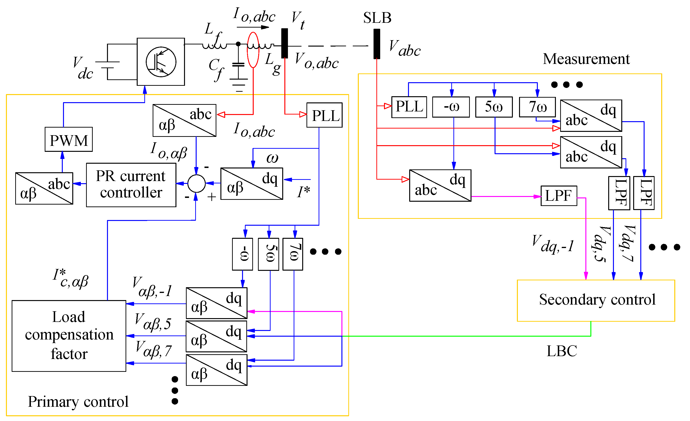
Figure 1 presents the proposed hierarchical plan for compensating for harmonics and voltage unbalance at SLB in a MG. The MG includes many current control IBDGs which are connected to the SLB by distribution lines. The inverters have LCL output filter, in which , and are inverter side inductance, network side inductance, and capacitor of the filter, respectively. The hierarchical control plan consists of two levels: primary and secondary. As shown in the figure, at first, the SLB voltage data are extracted by the measurement block and sent to the secondary control. This data includes the fundamental negative sequence component and positive components of selected harmonics.
Then, the secondary control should collect the required data from the measurement block and produce an appropriate reference control signal for IBDGs. The secondary controller can be far from the DGs and SLB. Thus, as shown in Figure 1, SLB voltage and frequency information are sent to this controller by means of Low Bandwidth Communication (LBC). In order to ensure that LBC is sufficient, the transmitted data should consist of approximately DC signals. Hence, the SLB voltage harmonic components are in dq (synchronous) reference frame. In local controllers, these signals are returned to the (stationary) reference frame for compensation. Details of the primary and secondary control plans is presented in the following section.
3.1. Secondary Control Level
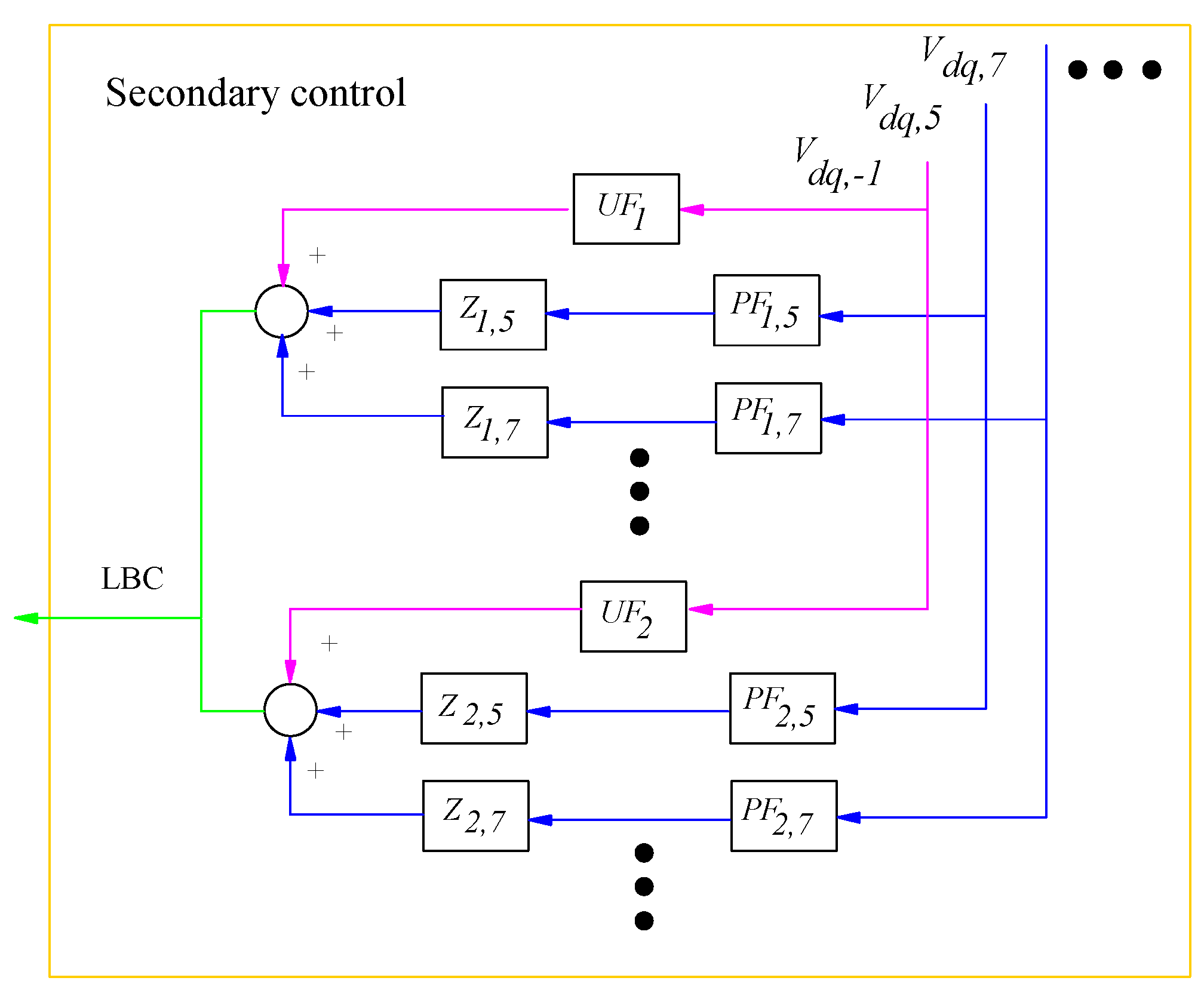
As shown in Figure 1, for extraction of the SLB voltage negative sequence component and main harmonics, the measured SLB voltage () is transformed to dq reference frames at −ω and other harmonic orders. ω is the system angular frequency estimated by a Phase Locked Loop (PLL). Afterwards, the second order Low Pass Filters (LPF) with cut-off frequencies of 2 Hz are used to extract , which are the dq components at negative sequence and harmonic frequencies. The block diagram of the central secondary controller is shown in Figure 2.
The generated signals in the measurement block should be modified according to the compensation priority indexes to improve compensation results. For this reason, the extracted harmonic is multiplied by the participation factor index and weighting factor , in which i represents bus number, and j denotes harmonic order [6]. The negative sequence component is also multiplied by the voltage unbalance factor () to determine the IBDGs contribution to the voltage unbalance compensation. The amount of UFi should be considered more in the buses that participate less in exciting critical modes, in order that these buses have a greater share in the unbalance compensation and vice versa. Hence, the compensation capacities of buses with a high participation factor in the critical modes are used more for the damping of corresponding harmonics.
3.2. Primary Control Level
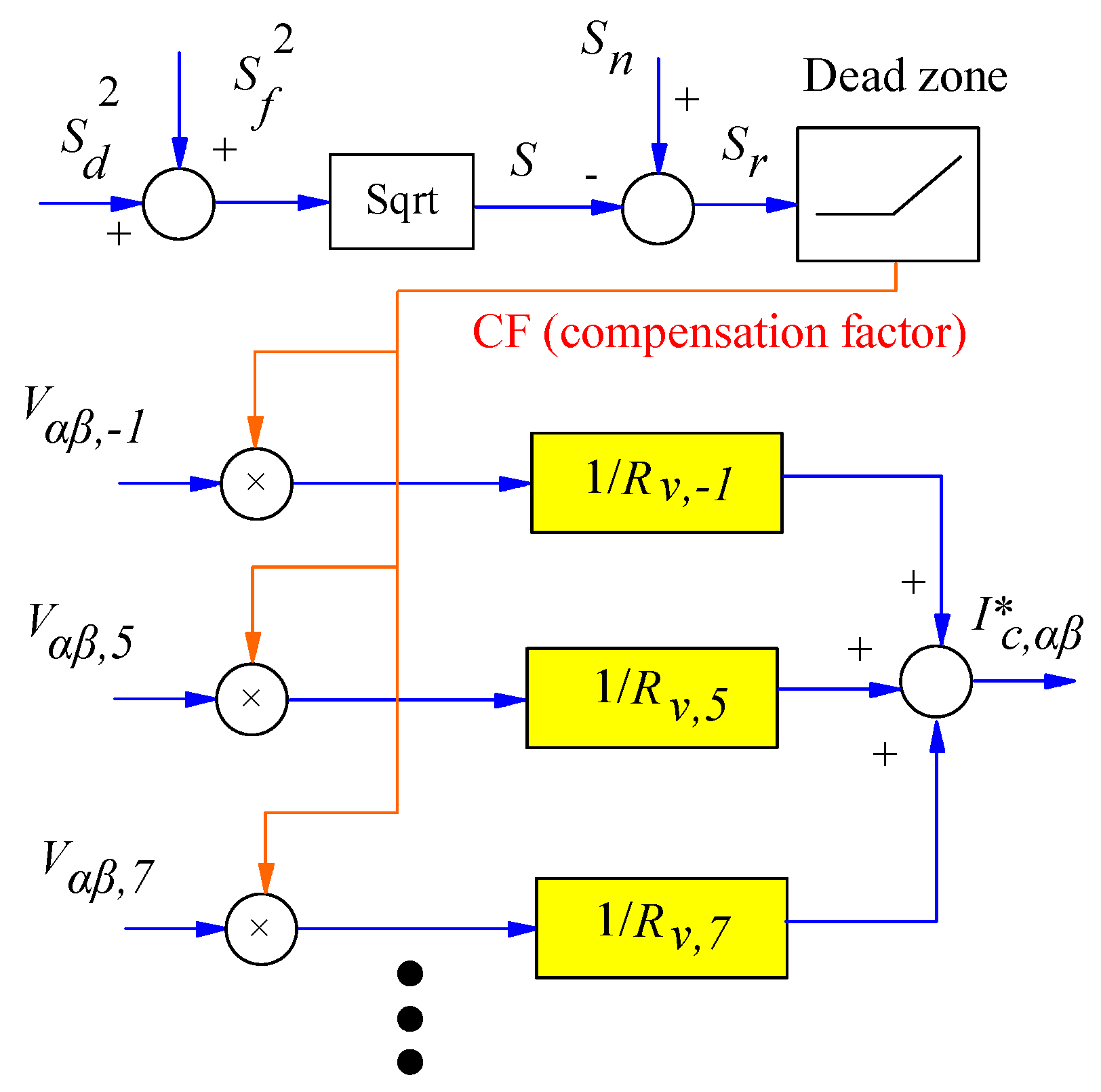
The detail of the primary control level of an IBDG is presented in Figure 3. The received signals from the secondary control level, after returning to stationary frame, are sent to the DG load compensation block. This block configures the compensation share of each IBDG according to its extra capacity.
As shown in this block Sn, Sf, Sd, S and Sr are nominal power of IBDG, positive sequence output power, distortion output power, total output power, and free capacity of IBDG, respectively. According to standards [19], the produced distortion power of each inverter can be calculated as follows:
where THDI and THDV are current and voltage total harmonic distortions. Afterwards, Sr can be calculated as shown in the figure, according to nominal power Sn and total output power S. The output signal of the dead zone block of this figure can be presented as follows [13]:
where j represents harmonic order. According to the Equation (8), if Sr > 0, with increasing in the total output power S, Sr reduces which represents reduction of IBDG load. In other words, there is inherited negative feedback in this equation which divides the compensation load between the IBDGs appropriately. Also, if Sr is less than zero, the dead zone block prevents any attempt of the compensation to avoid a DGs overload. The produced negative sequence component and voltage harmonic signals are sent to the virtual damping resistor block to multiply signals by . Afterwards, the compensation reference of each harmonic is generated separately, and then all of the compensation references are added together. Finally, total compensation reference is inserted as a current reference in the control system, as shown in Figure 1.
4. The MG Admittance Model
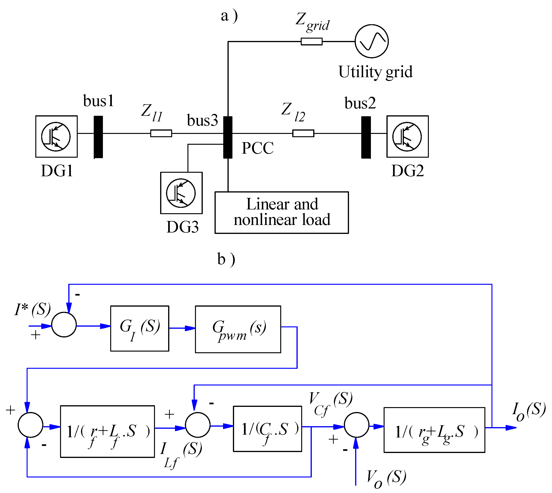
Figure 4a represents the single line diagram of a three-phase balanced MG. The implemented inverters are current control type and are used for supplying the pre-defined powers to the MG in connected operation mode. Also, and are the impedance of lines and grid impedance, respectively. Furthermore, many linear and nonlinear loads are also considered in this bus. The details of IBGD control system are shown in Figure 1. The inverter current control loop includes a Proportional Resonant (PR) controller that is designed in the stationary reference frame [20]. A PLL is used to synchronize the current control inverter with the MG.
The Pulse Width Modulation (PWM) converter is linearized around its operation point, and the relation between the inverter output current, reference current, and output voltage can be obtained as follows:
Equation (9) represents the Norton equivalent circuit of the current control inverter in which Gcc(S), Yoc(S) and are a closed loop transfer current function, output admittance, and reference current of the inverter, respectively. By using Figure 4b and employing Masson’s formula, Gcc(S) can be computed as:
Also, Yoc(S) can be calculated as:
where and are the internal resistances of the filter inductances. Also, GI(S) is the transfer function of the PR controller and is the transfer function of the PWM converter, that are written as:
where , , k, , and are resonance coefficient, proportional coefficient, harmonic order, fundamental frequency, and the converter switching period, respectively. In the following, the admittance matrix is constructed for the MG. In order to more precisely identify system resonances, the output impedance of IBDGs is considered in the MG admittance matrix.
where and are line and load admittances.
5. Identification of the Priority Factors
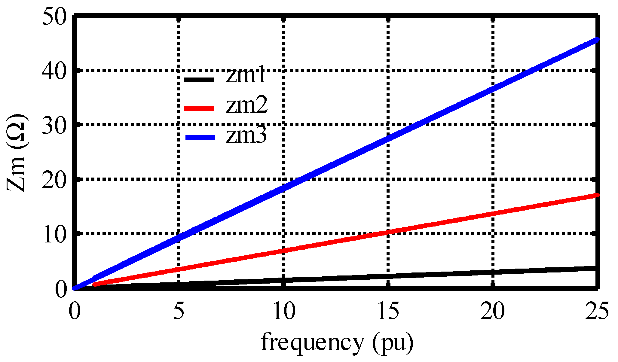
The resonance mode concepts presented in Section 2 are illustrated with a simple system shown in Figure 4a. There are three buses in the system in which harmonic resonance could be excited or observed. By considering the parameters of the control system and power circuit listed in Table 3, a modal impedance analysis is carried out for the MG to identify the participation factors of the buses. At first, in order to investigate the effect of inverter output impedance in the network resonances, a MG modal impedance analysis is carried out without considering the output impedance of the inverters. This is accomplished by replacing Equation (16) in Equations (1)–(6) and using the frequency scan of the obtained relationship. Regardless of the inverter output impedance, the MG behavior is the same as that of the inductance network; therefore, no resonance is observed in the system (Figure 5). The per-unit frequency is based on the fundamental frequency, and is equal to harmonic number.
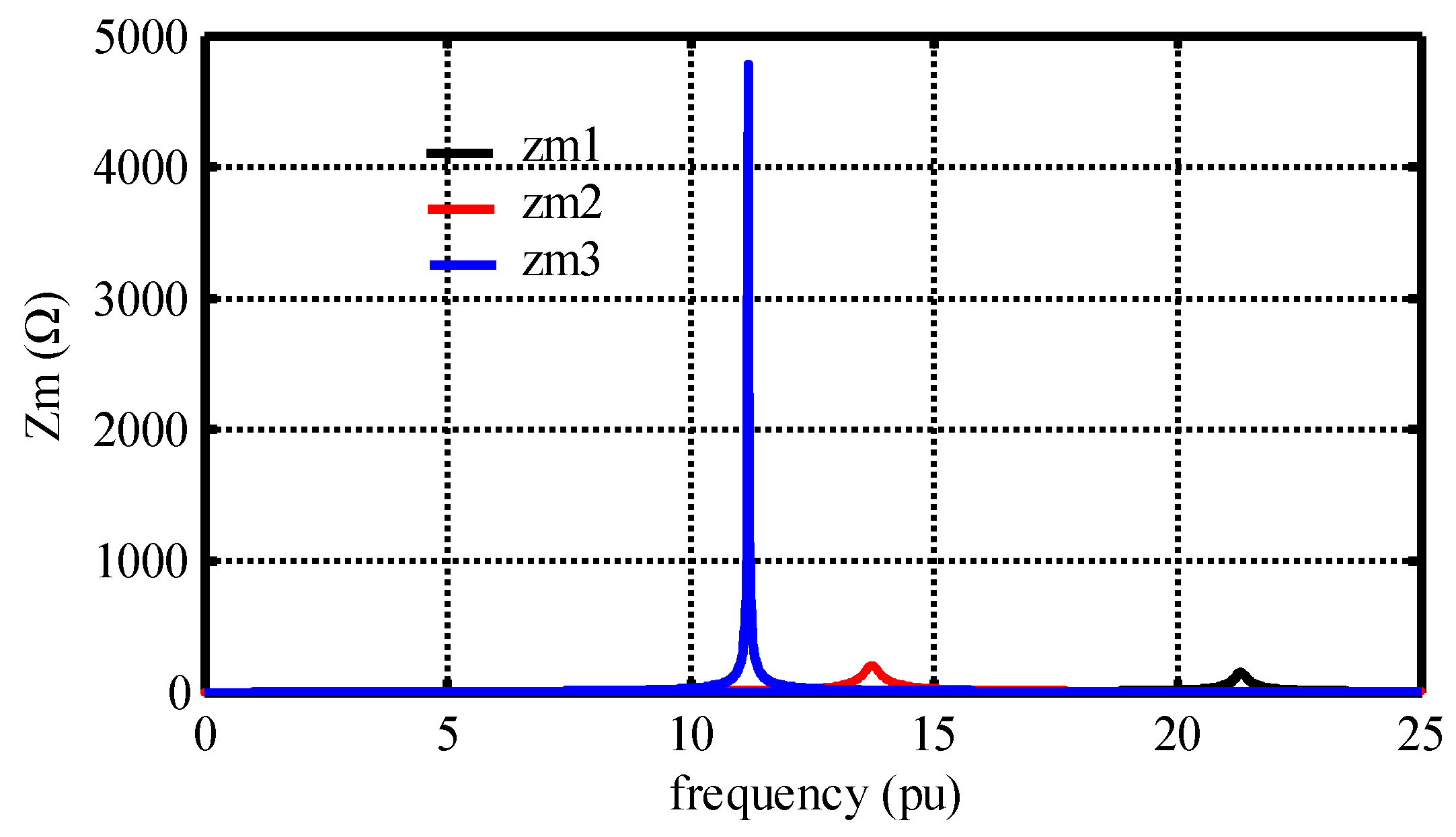
Considering the effect of inverter output impedance, due to the presence of capacitors in the inverter output filter, as shown in Figure 6, the magnitude of modal impedances have critical values in the low order frequencies. According to Table 1 and Figure 6, the maximum points in low order frequencies are related to the third and second modes which occur at harmonic orders 11.2 and 13.7, respectively. Bus 2 and 1 have the highest participation factor in creating these resonance modes. Therefore, the 11th harmonic at bus 2 and the 13th harmonic at bus 1 need to do more attenuation, and the compensation share of these two buses should be more than those of other IBDGs for these harmonics.
The MG resonances can be excited by the main grid. The resonance frequencies are also affected by the number of parallel inverters. Further considering that the main grid voltage often contains some low order steady state harmonics, significant steady state harmonic currents can be produced due to the effects of resonances. For example, when five parallel inverters with the same specifications are included in the MG, one of the resonance frequencies is around 350 Hz, which may excite the seventh steady state resonance in a 50 Hz system (Figure 7 and Table 2).
Due to the impacts of the aforementioned resonances, it can be concluded that neglecting the inverters output impedance in the modal impedance analysis, creates inaccuracy in the identification of bus participation factors, and the lines current quality can be severely distorted.
6. Simulation Results
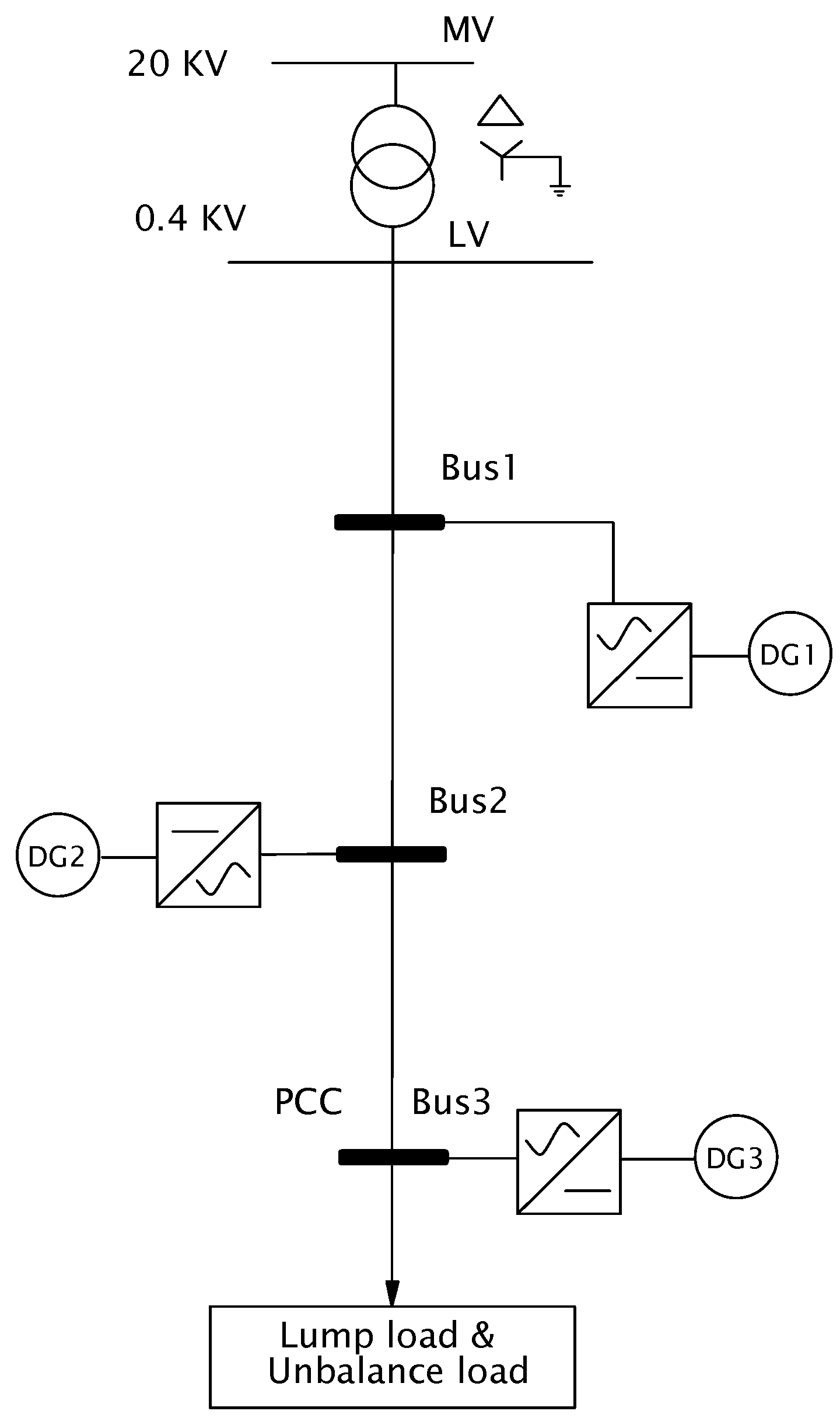
To test the effectiveness of the proposed approach, a test MG was built based on a system defined by NTUA, with slight changes used to test proposed control scheme. The electrical system comprises a MG and utility grid. Complete details of the test system and its power system parameters can be found in [21]. The MG single-line diagram is shown in Figure 8. All inverters operated in PQ control mode to supply a given active and reactive power set-point.
The control system parameters of DGs and loads are presented in Table 3. All the inverters have the similar parameters. A single-phase load is connected between phase A and phase B at PCC to create voltage unbalance. Also, in order to excite the MG resonances by the main grid, it is assumed that the grid voltage contains 7% seventh and 5% eleventh steady-state harmonics. The simulation is carried out in three steps:
- Step 1 (): DGs operate with only a fundamental controller, and harmonic compensation is not used.
- Step 2 (): harmonic compensation is added.
- Step 3 (): non-uniform harmonic compensation is activated.
6.1. Simulation Step 1
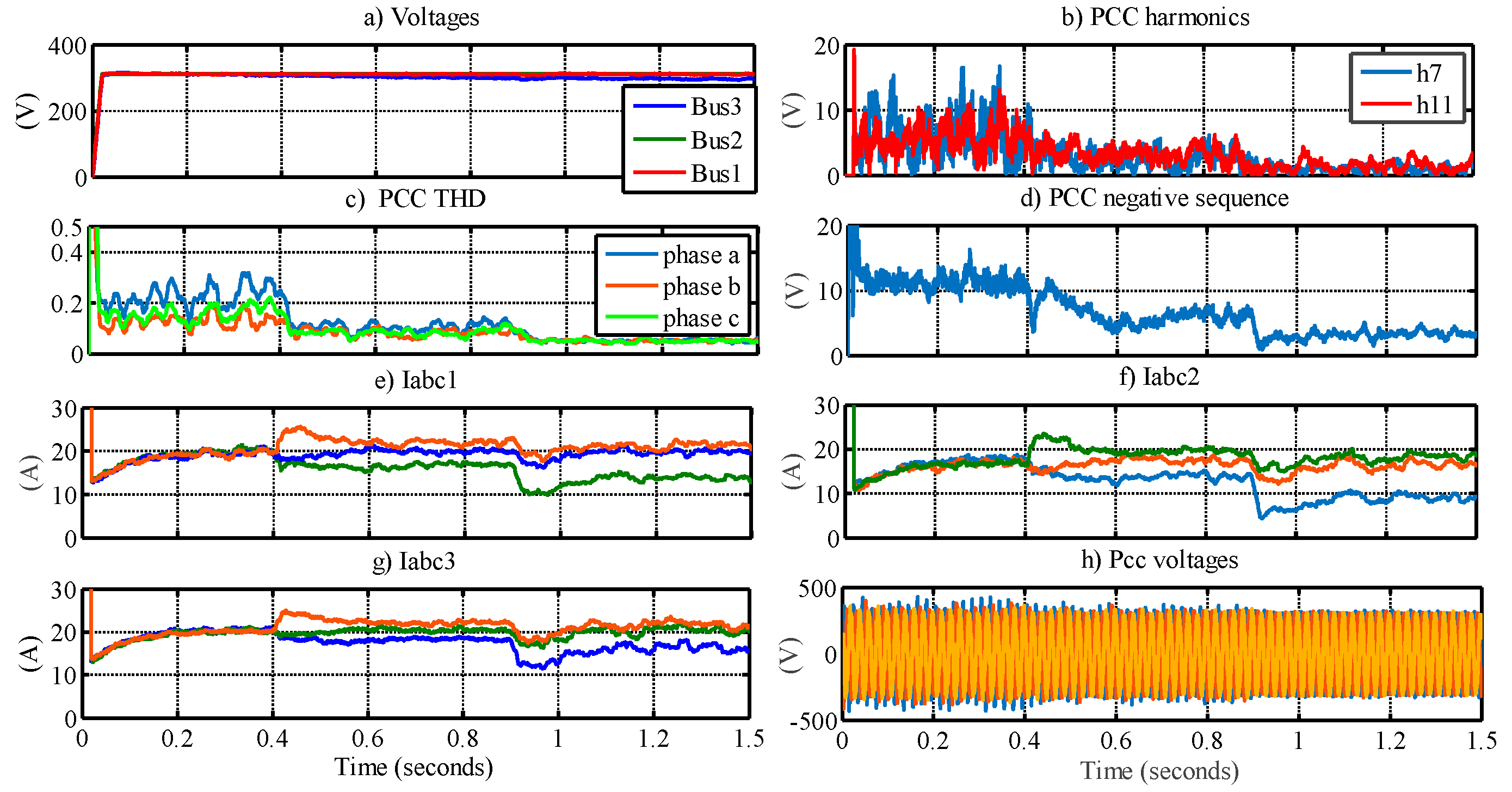
In this step, no compensation is carried out, and linear and unbalanced load are connected to the PCC. The simulation starts with zero initial values, and after the initial transient state, it goes to a stable state. As seen in Figure 9, before activating harmonic compensation, PCC voltage is distorted noticeably due to harmonics in the utility grid voltage and unbalanced load. This fact can be seen in Figure 9b–d as very high 7th and 11th harmonics, total harmonic distortions, and voltage unbalance (H7 and H11, THD and voltage negative sequence respectively) of PCC bus. The magnitude of voltage THD and the voltage negative sequence at bus 3 in an uncompensated state are almost 19% and 12 V. The output currents of inverters can be observed in Figure 9e–g. Also, the network voltages are shown in Figure 9a,h.
6.2. Simulation Step 2
At this stage, uniform compensation starts acting from t = 0.4 s. Regardless of the inverter output impedance, the DGs participate equally in harmonic and voltage unbalance compensation. The participation factors of IBDGs are the considered unit in the compensation, and all the DGs participate in the harmonics compensation with the same priority. This leads to a slight reduction of PCC voltage THD and voltage unbalance, according to the figures. Improvement of PCC voltage quality can also be observed in these figures. The amount of voltage THD and the voltage negative sequence at PCC bus in this state are reduced to 9% and 10 V, according to the figures.
6.3. Simulation Step 3
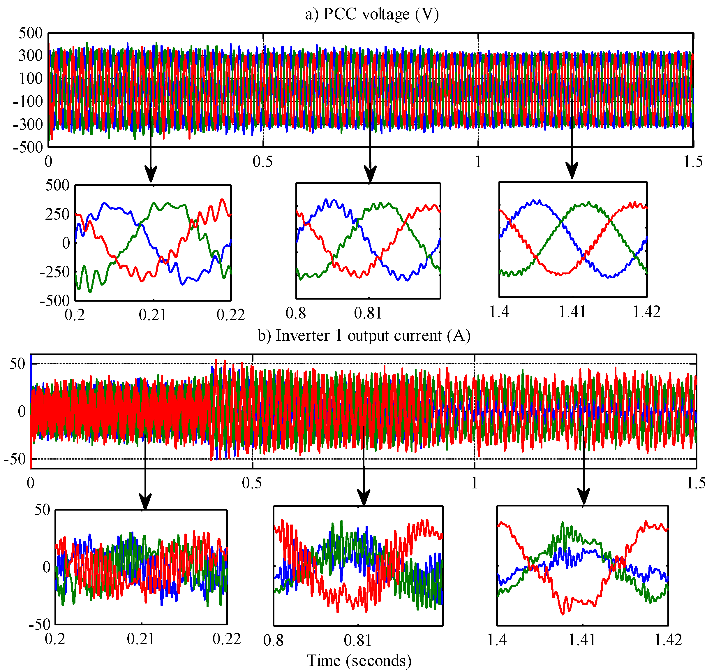
Finally, non-uniform compensation is activated at t = 0.9 s. In this case, the influence of IBDG output impedance and the coefficients of participation matrix are considered in the compensation. The normalized values of the system PF-matrix are used to assign DGs participation factors. This results in a significant reduction of PCC voltage THD and voltage unbalance compared to the previous section. Non-uniform compensation provides approximately sinusoidal voltage at PCC. In this method, voltage THD is reduced to 4%. The instantaneous waveforms of PCC voltage and inverter 1 output currents are shown in Figure 10 (with magnification).
According to these results, it is evident that, in the non-uniform compensation method, results are improved comparing to the traditional harmonic compensation method.
7. Conclusions
In this paper, a hierarchical compensation method for improving the voltage quality of SLB in a MG is presented. The compensation method is non-uniform, and compensation priorities for different DGs location and harmonic frequencies are identified for improved compensation performance compared to traditional compensation methods. The priority factors for compensation are identified by modal impedance analyses of the MG. The control method consists of two primary and secondary control levels. In the secondary control level, the values of compensation signals for the fundamental negative sequence component and positive components of selected harmonics are determined by the central secondary controller, according to the obtained priority coefficients, and then sent to the DGs local controllers. Assigning such compensation priorities to different IBDGs in the MG improves compensation performance, and harmonic distortion and voltage unbalance are divided between DGs appropriately. In the primary level, the load compensation factor of each DG is identified considering its extra capacity. The system is applicable to the tracking of reference currents and compensation for voltage harmonics and voltage unbalance at SLB. Simulation results prove the efficiency of the proposed method in different situations.
Author Contributions
All the authors have contributed to this article.
Funding
This research received no external funding.
Conflicts of Interest
The authors declare no conflict of interest.
References
- Arrillaga, J.; Watson, N.R. Power System Harmonics; Wiley: Hoboken, NJ, USA, 2003. [Google Scholar]
- Cheng, P.; Chen, C.; Lee, T.; Kuo, S. A cooperative imbalance compensation method for distributed-generation interface converters. IEEE Trans. Ind. Appl. 2009, 45, 805–815. [Google Scholar] [CrossRef]
- Savaghebi, M.; Jalilian, A.; Vasquez, J.C.; Guerrero, J.M. Autonomous voltage unbalance compensation in an islanded droop-controlled microgrid. IEEE Trans. Ind. Electron. 2013, 60, 1390–1402. [Google Scholar] [CrossRef]
- Lee, T.L.; Cheng, P.T. Design of a new cooperative harmonic filtering strategy for distributed generation interface converters in an islanding network. IEEE Trans. Power Electron. 2007, 22, 1919–1927. [Google Scholar] [CrossRef]
- He, J.; Li, Y.W.; Munir, M.S. A flexible harmonic control approach through voltage-controlled DG-grid interfacing converters. IEEE Trans. Ind. Electron. 2012, 59, 444–455. [Google Scholar] [CrossRef]
- Munir, M.S.; Li, Y.W.; Tian, H. Improved residential distribution system harmonic compensation scheme using power electronics interfaced DGs. IEEE Trans. Smart Grid 2016, 7, 1191–1203. [Google Scholar] [CrossRef]
- Munir, M.S.; Li, Y.W. Residential distribution system harmonic compensation using PV interfacing inverter. IEEE Trans. Smart Grid 2013, 4, 816–827. [Google Scholar] [CrossRef]
- Savaghebi, M.; Jalilian, A.; Vasquez, J.C.; Guerrero, J.M. Secondary control for voltage quality enhancement in microgrids. IEEE Trans. Smart Grid 2012, 3, 1893–1902. [Google Scholar] [CrossRef]
- Wada, K.; Fujita, H.; Akagi, H. Considerations of a shunt active filter based on voltage detection for installation on a long distribution feeder. IEEE Trans. Ind. Appl. 2002, 38, 1123–1130. [Google Scholar] [CrossRef]
- Swathi, K.; Bhavana, K. A hierarchical control approach for voltage unbalance compensation in a droop—Controlled micro-grid. IJCTA Int. Sci. Press 2016, 9, 213–223. [Google Scholar]
- Wu, L.; Yang, X.; Hao, X.; Lei, Y.; Li, Y.W. Network hierarchical control scheme for voltage unbalance compensation in an islanded microgrid with multiple inverters. ICIC Int. J. Innov. Comput. Inf. Control 2015, 11, 2089–2102. [Google Scholar]
- Hashempour, M.; Savaghebi, M.; Vasquez, J.C. Hierarchical control for voltage harmonics compensation in multi-area microgrids. In Diagnostics for Electrical Machines, Power Electronics and Drives (SDEMPED); IEEE: Guarda, Portugal, 2015; pp. 415–420. [Google Scholar] [Green Version]
- Savaghebi, M.; Jalilian, A.; Vasquez, J.C.; Guerrero, J.M.; Lee, T.L. Selective compensation of voltage harmonics in grid-connected microgrids. Math. Comput. Simul. 2013, 91, 211–228. [Google Scholar] [CrossRef] [Green Version]
- Savaghebi, M.; Shafiee, Q.; Vasquez, J.C.; Guerrero, J.M. Adaptive virtual impedance scheme for selective compensation of voltage unbalance and harmonics in microgrids. In Power and Energy Society General Meeting; IEEE: Denver, CO, USA, 2015; pp. 1–5. [Google Scholar] [Green Version]
- Han, Y.; Shen, P.; Zhao, X.; Guerrero, J.M. An enhanced power sharing scheme for voltage unbalance and harmonics compensation in an islanded AC microgrid. IEEE Trans. Energy Convers. 2016, 31, 1037–1050. [Google Scholar] [CrossRef]
- He, J.; Li, Y.W.; Bosnjak, D.; Harris, B. Investigation and active damping of multiple resonances in a parallel-inverter-based microgrid. IEEE Trans. Power Electron. 2013, 28, 234–246. [Google Scholar] [CrossRef]
- Bradt, M.; Badrzadeh, B.; Camm, E. Harmonics and resonance issues in wind power plants. In Transmission and Distribution Conference and Exposition (T&D); IEEE: Orlando, FL, USA, 2012; pp. 1–8. [Google Scholar]
- Xu, W.; Huang, Z.; Cui, Y.; Wang, H. Harmonic resonance mode analysis. IEEE Trans. Power Deliv. 2005, 20, 1182–1190. [Google Scholar] [CrossRef]
- IEEE Standard 1459–2010. Definitions for the measurement of electric power quantities under sinusoidal, nonsinusoidal, balanced or unbalanced conditions. In IEEE Transaction on Industry Applications; IEEE: Greenfield, WI, USA, 2010. [Google Scholar]
- Wang, X.; Blaabjerg, F.; Liserre, M.; Chen, Z.; He, J.; Li, Y. An active damper for stabilizing power-electronics-based ac systems. IEEE Trans. Power Electron. 2014, 29, 3318–3329. [Google Scholar] [CrossRef]
- Papathanassiou, S. Study-Case LV Network. Available online: http://microgrids.power.ece.ntua.gr/documents/Study-Case%20LVNetwork.pdf (accessed on 17 October 2014).
Figure 1.
Control structure and power section of the hierarchical control plan.

Figure 2.
Schematic control of the secondary level.

Figure 3.
The primary control level.

Figure 4.
(a) Single line diagram of the MG; (b) Block diagram of the inverter control system.

Figure 5.
Magnitude of network impedance modes.

Figure 6.
Impedance modes by considering the effect of IBDGs output impedance.

Figure 7.
MG impedance modes with five inverters.

Figure 8.
Single line of MG architecture, comprising DGs and loads.

Figure 9.
(a) The peak magnitude of phase voltage. (b) The magnitude of 7th and 11th voltage harmonics. (c) Voltage THD at PCC. (d) Negative sequence voltage at PCC. (e) The output currents of inverter 1. (f) The output currents of inverter 2. (g) The output currents of inverter 3. (h) Instantaneous voltages at PCC.

Figure 10.
(a) PCC voltages; (b) Output currents of inverter 1.


Table 1.
Critical impedances and participation factors.
| Harmonic Order | Critical Impedance | Participation Factor of | ||
|---|---|---|---|---|
| Bus 1 | Bus 2 | Bus 3 | ||
| 11.21 | 478.0 | 0.25 | 0.59 | 0.14 |
| 13.74 | 21.13 | 0.57 | 0.37 | 0.05 |
| 21.32 | 15.13 | 0.16 | 0.02 | 0.80 |
Table 2.
MG participation factors with five inverters.
| Harmonic Order | Critical Impedance | Participation Factor of | ||
|---|---|---|---|---|
| Bus 1 | Bus 2 | Bus 3 | ||
| 7.18 | 87.8 | 0.29 | 0.51 | 0.62 |
| 9.07 | 206.82 | 0.45 | 0.49 | 0.25 |
| 17.13 | 658.85 | 0.33 | 0.04 | 0.86 |
Table 3.
Parameters of load and control system.
| Symbol | Parameter | Value | Unit |
|---|---|---|---|
| Voltage of DC link | 650 | V | |
| Balanced load | 5 + j6 | Ω | |
| Unbalanced load | 20 + j6.5 | Ω | |
| Filter inductances | 0.2, 1.8 | mH | |
| Switching frequency | 10 | kHZ | |
| ,,, | Virtual resistances | 9 | Ω |
| Filter capacitor | 25 | μF | |
| Controller coefficients | 1, 100 | - | |
| Unbalance factors | 0.5, 0.5, 1 | - |
© 2018 by the authors. Licensee MDPI, Basel, Switzerland. This article is an open access article distributed under the terms and conditions of the Creative Commons Attribution (CC BY) license (http://creativecommons.org/licenses/by/4.0/).
Share and Cite
MDPI and ACS Style
Afrasiabi, M.; Rokrok, E. An Improved Centralized Control Structure for Compensation of Voltage Distortions in Inverter-Based Microgrids. Energies 2018, 11, 1862. https://doi.org/10.3390/en11071862
AMA Style
Afrasiabi M, Rokrok E. An Improved Centralized Control Structure for Compensation of Voltage Distortions in Inverter-Based Microgrids. Energies. 2018; 11(7):1862. https://doi.org/10.3390/en11071862
Chicago/Turabian StyleAfrasiabi, Morteza, and Esmaeel Rokrok. 2018. "An Improved Centralized Control Structure for Compensation of Voltage Distortions in Inverter-Based Microgrids" Energies 11, no. 7: 1862. https://doi.org/10.3390/en11071862
Note that from the first issue of 2016, this journal uses article numbers instead of page numbers. See further details here.