Review

Complex Nanostructures: Synthesis and Energetic Applications

Department of Chemistry, Merkert Chemistry Center, Boston College, 2609 Beacon St., Chestnut Hill, MA 02467, USA
*
Author to whom correspondence should be addressed.
Energies 2010, 3(3), 285-300; https://doi.org/10.3390/en3030285
Submission received: 28 December 2009 / Accepted: 3 February 2010 / Published: 26 February 2010
(This article belongs to the Special Issue Solar Cells)

Abstract

:
Connected through single crystalline junctions, low dimensional materials such as nanowires and nanorods form complex nanostructures. These new materials exhibit mechanical strengths and electrical conductivities superior to their constituents while maintaining comparable surface areas, an attribute ideal for energetic applications. More efficient solar cells, higher capacity batteries and better performing photoelectrochemical cells have been built using these materials. This article reviews this exciting new class of materials and covers topics from controlled syntheses to applications in photovoltaics, chemical energy conversion and electrical charge storage. Mechanisms responsible for the improved performance are discussed. The prospect of their applications in a broader energy-related field is analyzed.

1. Introduction

The interconversion of different forms of energy is dictated by thermodynamics, the detail of which has been worked out a few decades ago. Under one sun conditions and where a single p/n junction is involved, the efficiency that solar energy can be converted into electrical energy falls below the Shockley-Queisser limit, ~31% at room temperature [1]. A similar efficiency limit is present for the conversion of solar energy into chemical energy where a solid-liquid junction is involved [2]. As Earth is blessed with abundant sunlight, these efficiency limits are reasonable. In fact, devices performing with efficiencies near the theoretical limit have been created [3]. More broadly, being able to convert the sunlight into electricity or chemicals at efficiencies only half of these limits would provide ample usable energy that suffices our needs without devastating the environment [4,5]. However, this prospect has been plagued by the cost-efficiency dilemma—efficient devices are prohibitively costly while inexpensive devices fail to deliver practical efficiencies. Despite decades of research, limited progress has been made. To date, only a small fraction of our energy usage comes from the sunlight directly. Such a situation creates a host of challenges that we must face now. Because the theoretical aspects of the energy interconversion have been worked out, the key to meeting these challenges lies in material innovations, so as to break the cost-efficiency dilemma.
By example, we next use the photo-to-electricity conversion consideration to illustrate the root of the cost-efficiency dilemma. In a simplistic form, the material of choice for efficient photo-to-electricity conversion must meet the following requirements: good light absorption, effective charge separation, efficient charge collection and outstanding charge transport [1,6]. It is extremely difficult to balance these needs for optimized performance because these requirements often compete with each other. Complete light absorption, for instance, favors thick materials whereas charge collection and charge transport is more effective when the material is thinner. There exist material candidates with intrinsic properties that satisfy these needs, and these materials are mainly exotic compounds such as II-VI and III-V semiconductors. They are nevertheless scarce hence highly expensive. Alternatively, one can labor to perfect devices made of earth abundant materials, which exhibit less optimum properties, by balancing various factors as discussed above. The optimization itself, however, is extraordinarily complex and therefore leads to high cost, as well [7]. The difficulty is exacerbated when photo-to-chemical conversion is considered where chemical stability further limits the choice of materials. In efforts to lower the cost, approaches have also been developed based on radically new ideas. Easy-to-process organic compounds such as conducting polymer or dye sensitizers, for instance, have been studied [8,9,10]. These devices still perform at efficiencies far below the theoretical limit, making the approach uncompetitive at the present stage.
With the development of nanoscale materials in the past decade, a great deal of attention has been attracted to exploring this new class of materials for efficient energy conversion [11]. The interest stems from the relevant length scale of these materials to that of charge behaviors in solids [12]. For example, the characteristic dimension of charge separation and charge diffusion, which are dependent on the depletion region width and the typical minor carrier diffusion length, respectively, usually falls in the nanoscale. Materials of similar length scale are therefore expected to offer unprecedented opportunities in controlling charge behaviors for highly efficient energy conversion. In addition, different from bulk crystals, nanomaterials are easy to synthesize and are often produced at high quantity and high quality under mild conditions, promising low-cost production. Taken as a whole, nanomaterials hold great potential in breaking the cost-efficiency dilemma.
One of the most studied attributes of nanomaterials for energy related applications is the high surface area. The high surface roughening factor (>1,000) that TiO2 nanoparticles exhibit, for example, plays a critical role in enhancing the performance of TiO2-based dye sensitized solar cells [10]. However, when similar approaches are extended to other semiconductor nanoparticles, researchers encounter a great hurdle – the poor charge transport through discrete nanoparticles due to the following reasons. First, charges travel between adjacent nanoparticles mainly through hopping, a process neither efficient nor fast. Second, the high density of defects on the surface of nanoparticles, both crystallographic and electronic, acts as traps to hinder charge transport. To circumvent this problem, Alivisatos and others have devised to use anisotropic nanostructures such as nanorods as charge collection and transport components in hybrid solar cells [13]. In this application nanostructures do not participate in light absorption—they only act to scavenge and transport charges to the external electrodes. One-dimensional nanostructures such as nanotubes and nanowires have been recently studied intensively based on similar considerations of better charge collection and transport [14,15,16,17,18]. While improving the electronic properties, one-dimensional nanostructures fail to provide comparable surface areas as that of nanoparticles. Additionally, phase segregation often occurs when nanorods are used, leading to further surface area reduction.
To achieve both high surface area and superior charge transport capabilities, researchers have turned to complex nanostructures, which are formed by an ensemble of anisotropic nanostructures such as nanorods or nanowires connected through single crystalline junctions [19,20,21,22,23,24,25]. These new materials offer the following chief advantages: (i) the single crystalline nature of each constituent beam and the junctions renders the entire structure to perform superiorly in collecting and transporting charges; (ii) the complex nature of the structure offers surface areas comparable to that found in structures formed by nanoparticles; (iii) the mechanical strength offered by the crystalline junctions helps separate the individual beams of a complex structure, preventing the structure from collapsing that will lead to surface area reduction. Nevertheless, we note that despite these advantages the design principle of complex nanostructures still leaves one challenge outstanding when solar energy conversion is concerned, namely the intrinsic material properties of photoactivity. Heteronanostructures consisting of more than one component hold answers to this challenge, because each component may be optimized separately to achieve desired overall properties in a concerted manner. The advantages of this aspect will be discussed in this article as well.
In addition to solar energy conversion, the high surface area, superior electrical conductivity and excellent mechanical strength of complex nanostructures are also found beneficial to electrical charge storage applications. When combined with high capacity materials, complex nanostructures serve as the scaffold to produce high performance anode materials for Li ion batteries [26].
This article reviews the exciting new material of complex nanostructures. We discuss various aspects of the material, ranging from controlled syntheses to applications in photovoltaics, chemical energy conversions and electrical charge storage. This goal is achieved by using TiSi2 nanonets that are produced in our lab by chemical vapor deposition (CVD) and nanostructures with similar complexities created by others as examples.

2. Synthesis and Structure of Complex Nanostructures

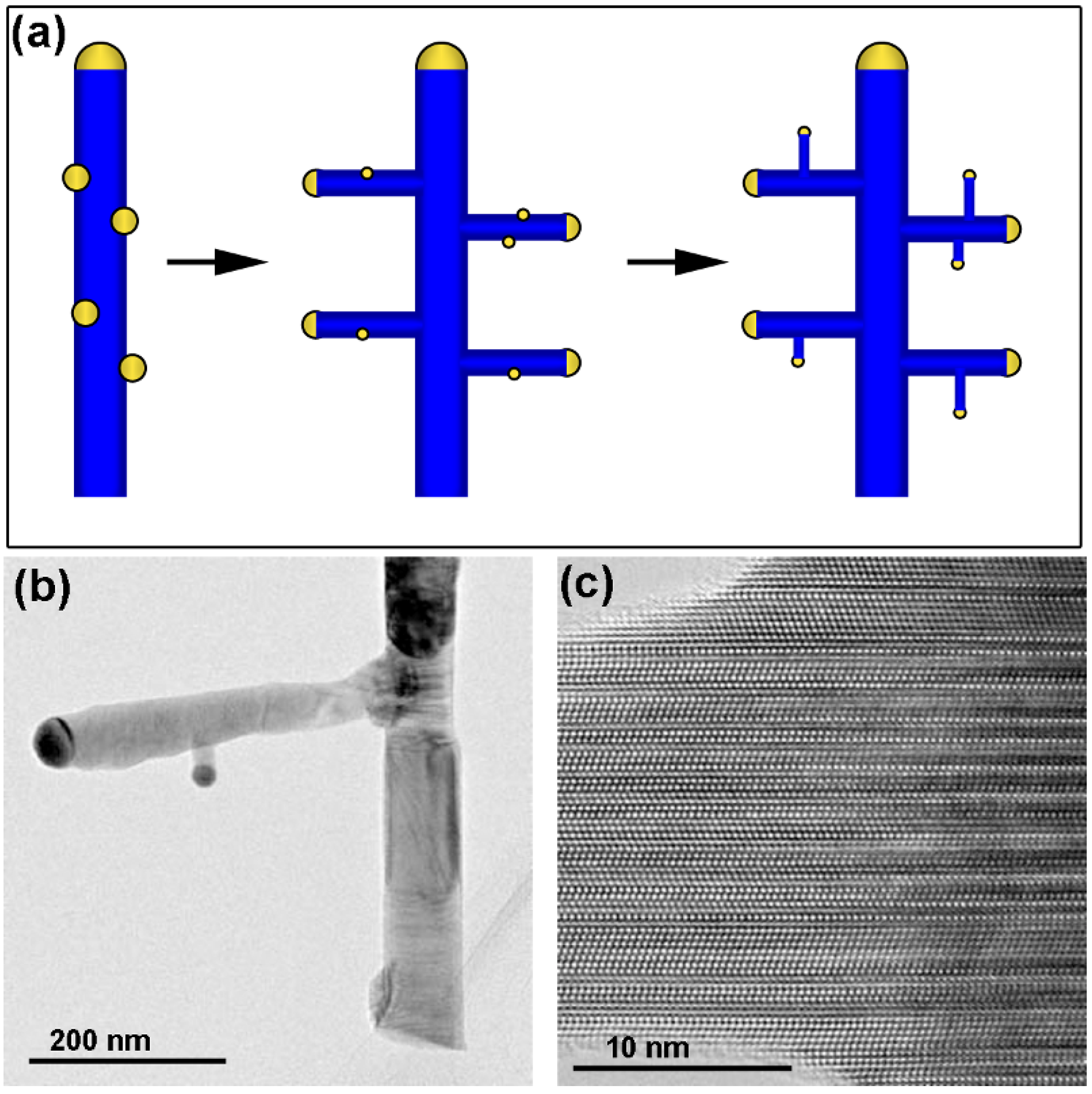
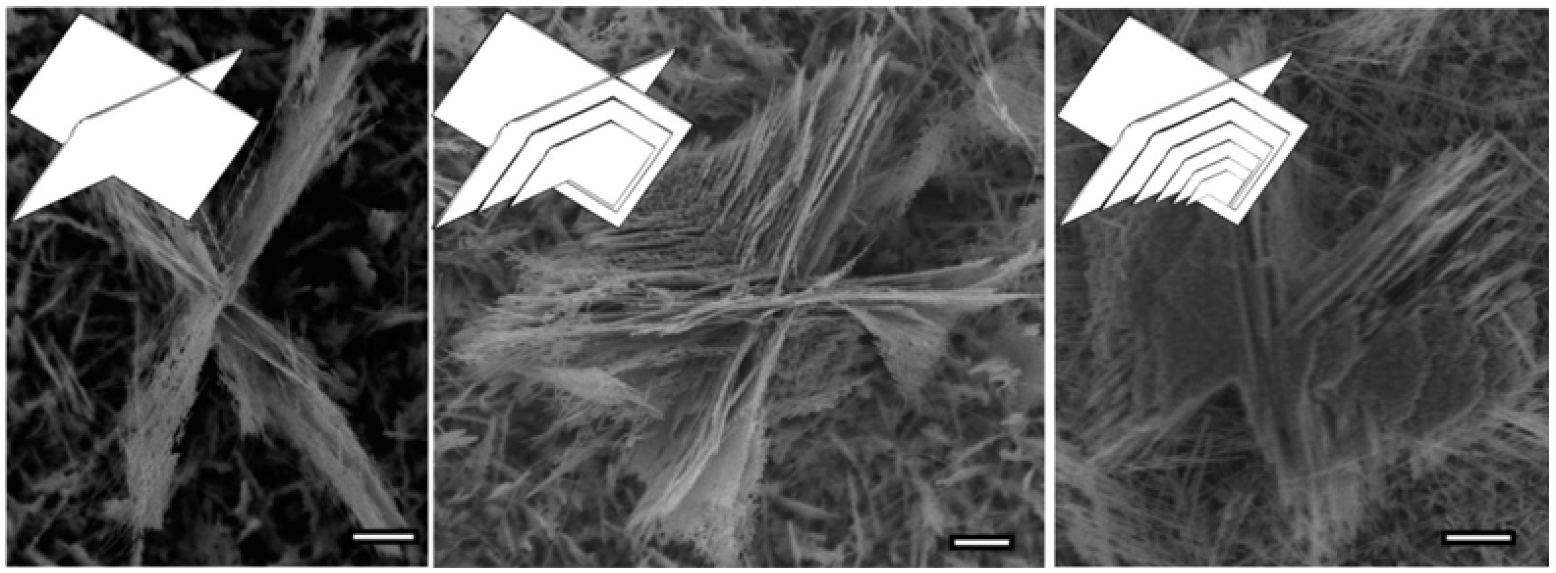
2.1. Controlled branching through sequential seeding

Built upon the widely studied vapor-liquid-solid (VLS) mechanism [27], the sequential seeding method represents a rational approach toward complex nanostructures [22]. In essence, this approach involves several steps of VLS nanowire growth, each stage producing one generation of branches (Figure 1). The first growth creates the main trunk of the final structure; this step is followed by a seeding process that produces nanowires coated with newly dispersed growth seeds, ready for the second growth. The second growth produces nanowires rooted on the main trunk obtained previously. These newly grown nanowires can be regarded as the first generation of branches. They are joined to the main trunk by high quality crystalline junctions. Another seeding process follows this growth and readies the already branched nanostructures for yet a third growth, producing the second generation of branches. When the seeding and growth processes are carried out in a sequential manner, a hierarchical complex nanostructure is produced. The strength of this approach lies in the rational control of the branching and the utilization of the well-established VLS growth mechanism. The exact locations where the seeds are dispersed, however, are difficult to control. The resulting nanostructures therefore tend to vary in morphologies. This approach has been applied to Si [22], GaP [28], PdSe [29], InAs [30] and indium tin oxide [31] nanostructures. In a slight variation, this strategy has also been applied to solution phase synthesis such as the solution-liquid-solid (SLS) growth [32]. Importantly, the branches of complex nanostructures created by this approach can be of different composition from that of the trunk, as has been demonstrated in examples of ZnO/In2O3 [33], ZnO/SnO2 [32], CdS/ZnS [34], In2O3/ITO [35] and carbon nanotube/SiC [36].
Figure 1. Branched nanowires synthesized through sequential seeding following the VLS growth processes. (a) A schematic illustration of the process. (b) Transmission electron micrograph showing the main trunk (vertical) and two generations of branches. (c) High resolution imaging reveals the single-crystalline nature of the junctions that connect the trunk and branch nanowires (reproduced with permission from Nature Publishing Group [28]).
Energies 03 00285 g001

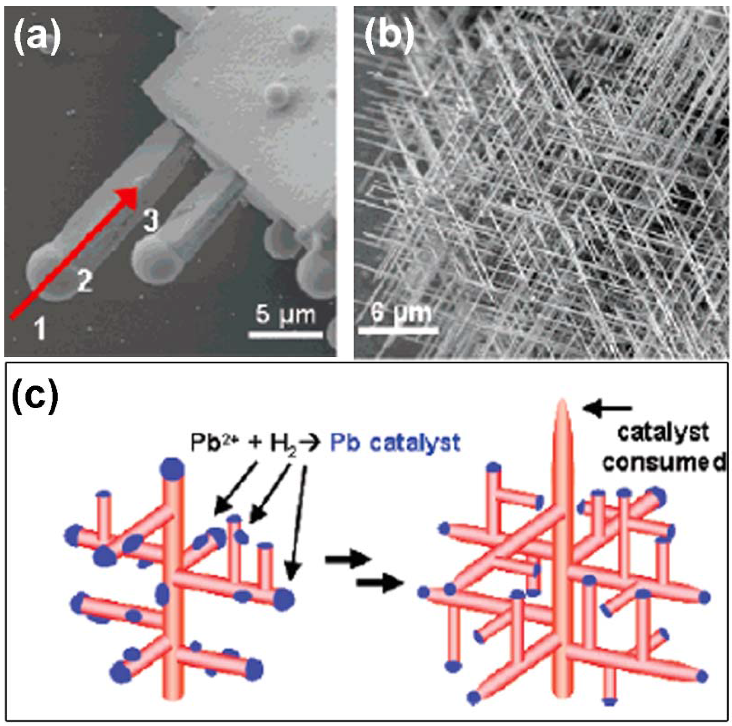
2.2. In situ seeding introduced branching

Crystals with high symmetries such as the cubic structure tends to grow in an isotropic fashion. PbS and PbSe fall in this category. During the synthesis of PbS and PbSe, catalysts in the form of Pb nanoparticles can be formed in situ in the reaction system. The formation of the catalyst helps break the crystal growth isotropy and creates hyperbranched three-dimensional (3D) structures [37]. Compared with the sequential seeding approach, the in situ seeding process is easy to implement as a continuous growth can be maintained. However, because the nanowire growth and catalyst generation take place simultaneously, the “generations” of the branches are not well defined. Experimentally, success requires the delicate control of gas precursors, proper selection of catalyst, and is so far only limited to a handful of chalcogenide systems [38]. Intriguingly, when the branching events occur simultaneously with the crystal twist as induced by nucleation from screw dislocations, novel pine-tree structures can be obtained [39,40].
Figure 2. Hyperbranched PdSe nanowire network catalyzed by in situ generated Pb seeds. (a) An SEM image showing PbSe microrods with residual Pb catalyst caps. Chemical analysis along the red arrow confirmed the Pb/PbSe cap/nanowire composition. (b) An SEM image showing the 3D PdSe nanowire network. (c) A schematic illustration showing the in situ generation and consumption of the Pb catalysts during the growth. (Left) Pb2+ was reduced to Pd catalysts that deposited on an existing network; (Right) New branches were grown from the catalysts, while an old branch (marked by the arrow) stopped to grow when the catalyst was completely consumed (reproduced with permission from American Chemical Society [41]).
Energies 03 00285 g002

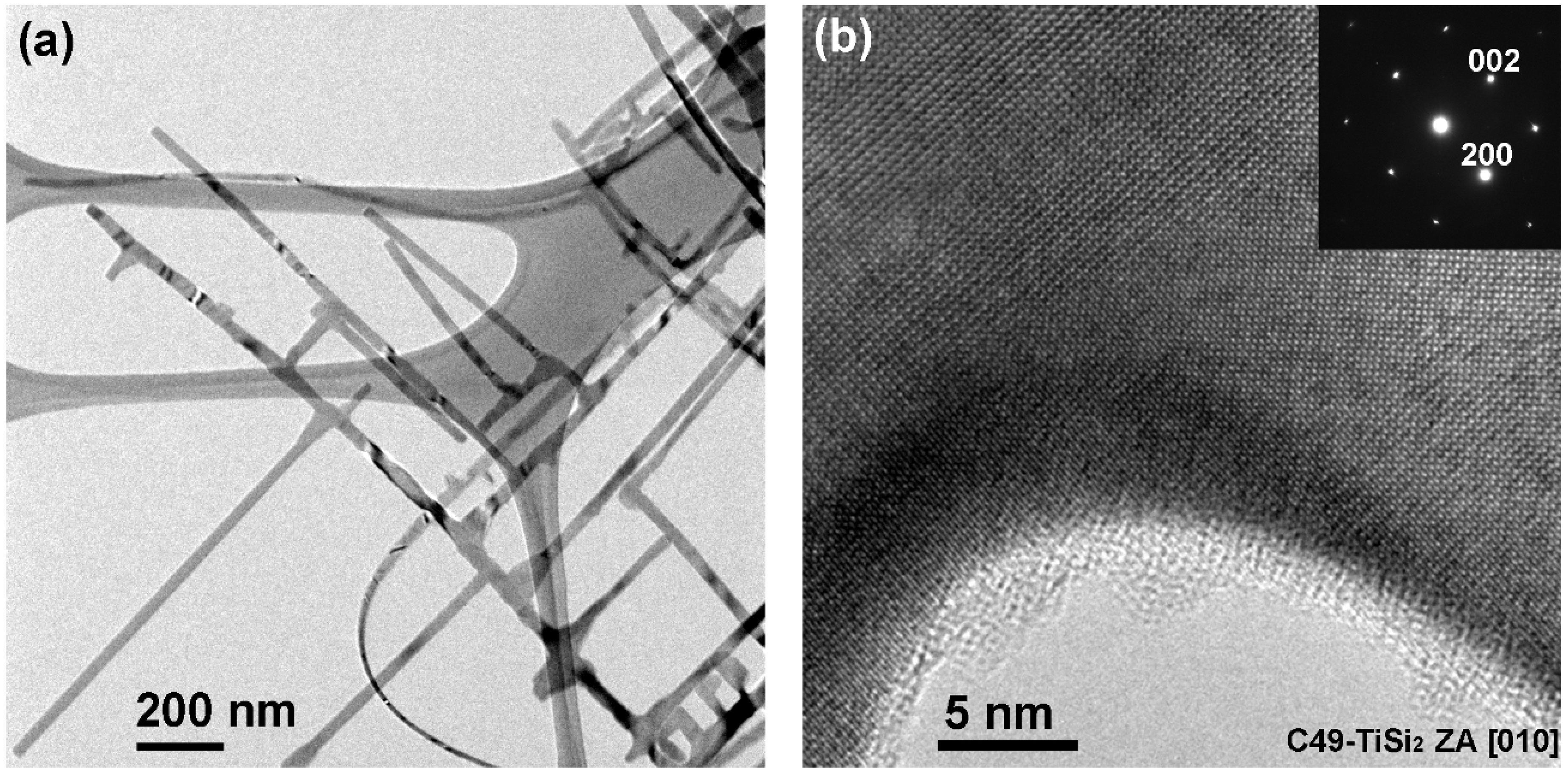
2.3. Phase transition introduced branching

Branched nanostructures can also be obtained without the use of catalyst if a phase transition occurs during crystal growth. CdTe tetrapods synthesized by Alivisatos et al. represents a good example of this phenomenon [42,43]. In a homogeneous solution where catalyst is absent, the initial CdTe colloids are of the cubic zinc-blende (ZB) structure. When the crystal size exceeds a critical size (approximately 3 nm in the case of CdTe), introduction of stable stacking faults in the ZB structure leads to the formation of a hexagonal segment. Further growth adopts the hexagonal stacking sequence to produce wurtzite (WZ) pods. Homogeneous junctions are produced between the core and the four pods (Figure 3). The branching due to the ZB-WZ phase transition is related to the size-dependent phase stability of the material. Similar ZnO tetrapods, albeit much larger, were also observed, which also have a ZB core but WZ branches [44].
Figure 3. Phase transition introduced branching. (a) The mechanism is schematically shown, where the WZ branches grow from a ZB core [19]. (b) Similar branch formation has been observed on ZnO structure as well [44]. (c) The atomic structure of the junction is resolved by HRTEM imaging for the CdTe tetrapods [43]. Reproduced with permission from American Institute of Physics and Nature Publishing Group.
Energies 03 00285 g003

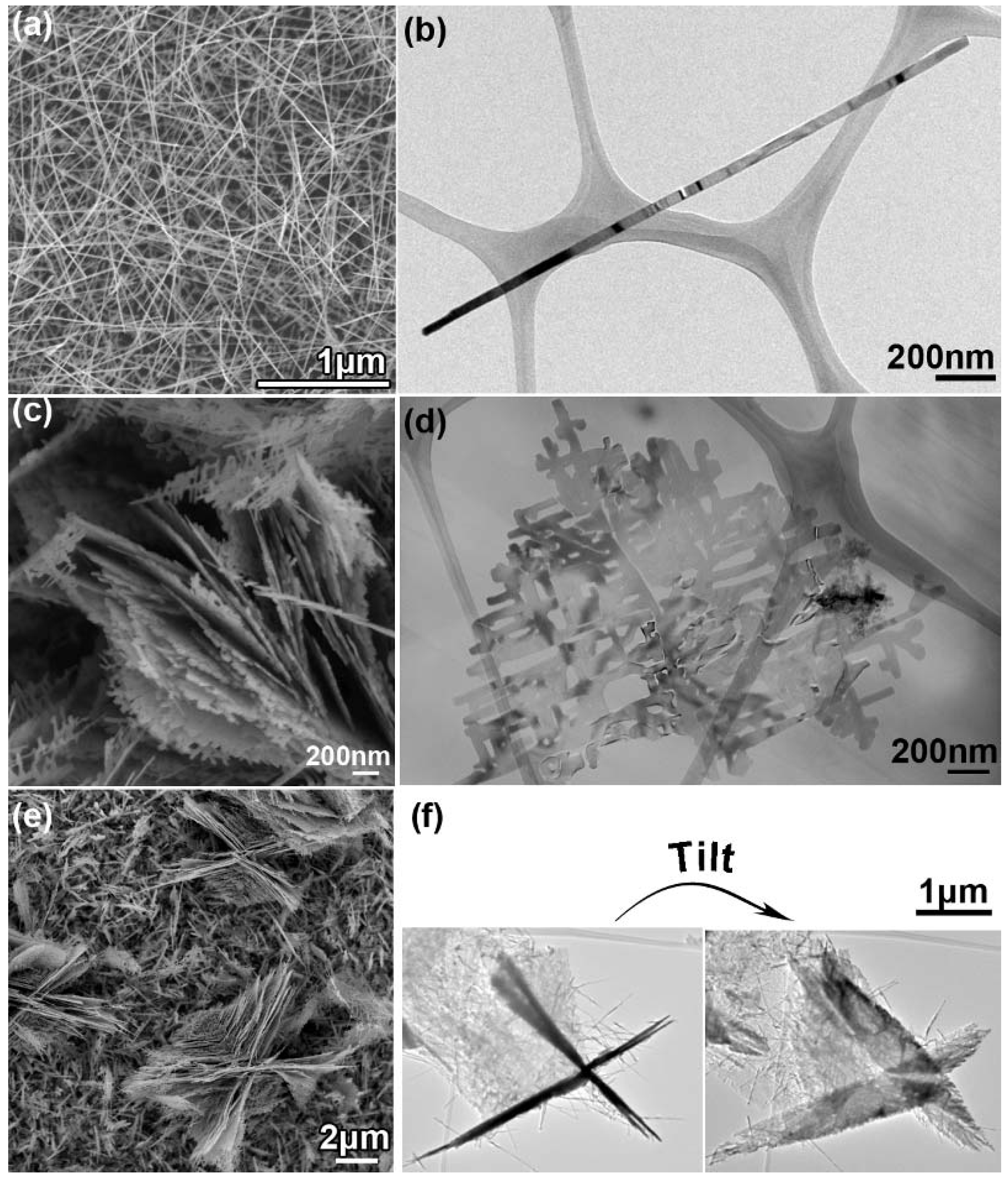
2.4. Surface energy difference introduced branching

For growths where the crystal structure is uniform and heterogeneous catalyst is absent, the surface energy differences of different crystal planes can be exploited to achieve anisotropic growth and to produce complex nanostructures. Based on this consideration, we have successfully synthesized a unique two-dimensional (2D) TiSi2 nanonet structure [23,25]. The 2D morphology originated from the crystal anisotropy of C49 TiSi2 and selective passivation of crystal planes during the synthesis. Specifically, the (010) plane of C49 TiSi2 is terminated by Si layers that can be passivated by H and Cl atoms. This passivation hinders further addition of Ti and Si species hence the growth along this direction. Under conditions that favor such passivation, the growth takes place exclusively along the <100> and <001> directions, yielding nanonets with single crystalline right-angled junctions (Figure 4).
Figure 4. 2D TiSi2 nanonets were obtained by adjusting growth conditions to achieve desired surface energy differences between various TiSi2 crystal planes. (a) The morphology is clearly revealed in this low magnification TEM [23]. (b) Atomic lattice resolved high resolution imaging confirms the single-crystalline nature of a junction. The inset electron diffraction pattern was taken along the [010] zone axis (ZA) of the C49 TiSi2 phase. Reproduced with permission from Angewandte Chemie.
Energies 03 00285 g004
The passivation of the (010) plane can be disrupted by change of growth conditions. The increase of Ti-containing species, for instance, induces the breaking of the Si layer passivation, leading to more complex nanostructure formation. Taking advantage of this property, we have studied how the growth conditions influences the growth and synthesized TiSi2 nanostructures of different complexities, ranging from 1D nanowires, to 2D nanonets and to 3D nanostructures (Figure 5) [25]. Intriguingly, the 1D TiSi2 nanowires are of the C54 phase while the 3D structure is a special assembly of 2D nanonets. Careful TEM studies show that the C54 nanowires are grown along the <010> direction, while the 3D structures are grown from a distorted C54 base [23]. Sequential adding of the 2D flaps leads to growth of the 3D ordered structure (Figure 6). Despite the sensitivity to the growth conditions, we were able to obtain high yield and high purity products with desired morphologies through controlling the growth conditions.
Figure 5. TiSi2 nanostructures of varying complexities [25]. (a,b) 1D C54-TiSi2 nanowires. (c,d) 2D C49-TiSi2 nanonets. (e,f) 3D C49-TiSi2 structure. The left and right panels are SEM and TEM images, respectively. Reproduced with permissions from American Chemical Society.
Energies 03 00285 g005
Figure 6. The progression of the TiSi2 complex nanostructures during a growth is revealed in this SEM image series. Scale bars: 1 μm [25]. Reproduced with permissions from American Chemical Society.
Energies 03 00285 g006
One surprising finding of the TiSi2 nanonets is the high conductivity as measured using the STM-TEM method (Figure 7). The measured conductivity of ρ ~10 μΩ-cm is comparable to that of bulk C54 TiSi2 and is approximately 10-times better than bulk C49 TiSi2. We attributed this high conductivity to the lack of defects in the nanoscale C49 TiSi2 structures; the high density of such defects in bulk C49 TiSi2 was found responsible for its low conductivity [45,46,47]. The conductive TiSi2 nanonets can be readily collected on various substrates for efficient charge transport functionalities. In the next section, we will show that the complex nanostructures of TiSi2 are excellent choice for electron transport, opening up the opportunity to use them as scaffold for various energy related applications.
Figure 7. The electrical conductivity of TiSi2 nanonet was measured using a unique STM-TEM setup [23]. The tip that was used to contact the nanonet is shown in (a) & (b). Note that the nanonet rolls up when pushed by the mobile STM probe. It exhibits excellent mechanical strength and flexibility since the large deformation can be recovered completely without damage of the structure. (c) A current-voltage curve is recorded and used to calculated the nanonets’ electrical conductivity. Reproduced with permissions from Angewandte Chemie.
Energies 03 00285 g007

3. Applications of Complex Nanostructures

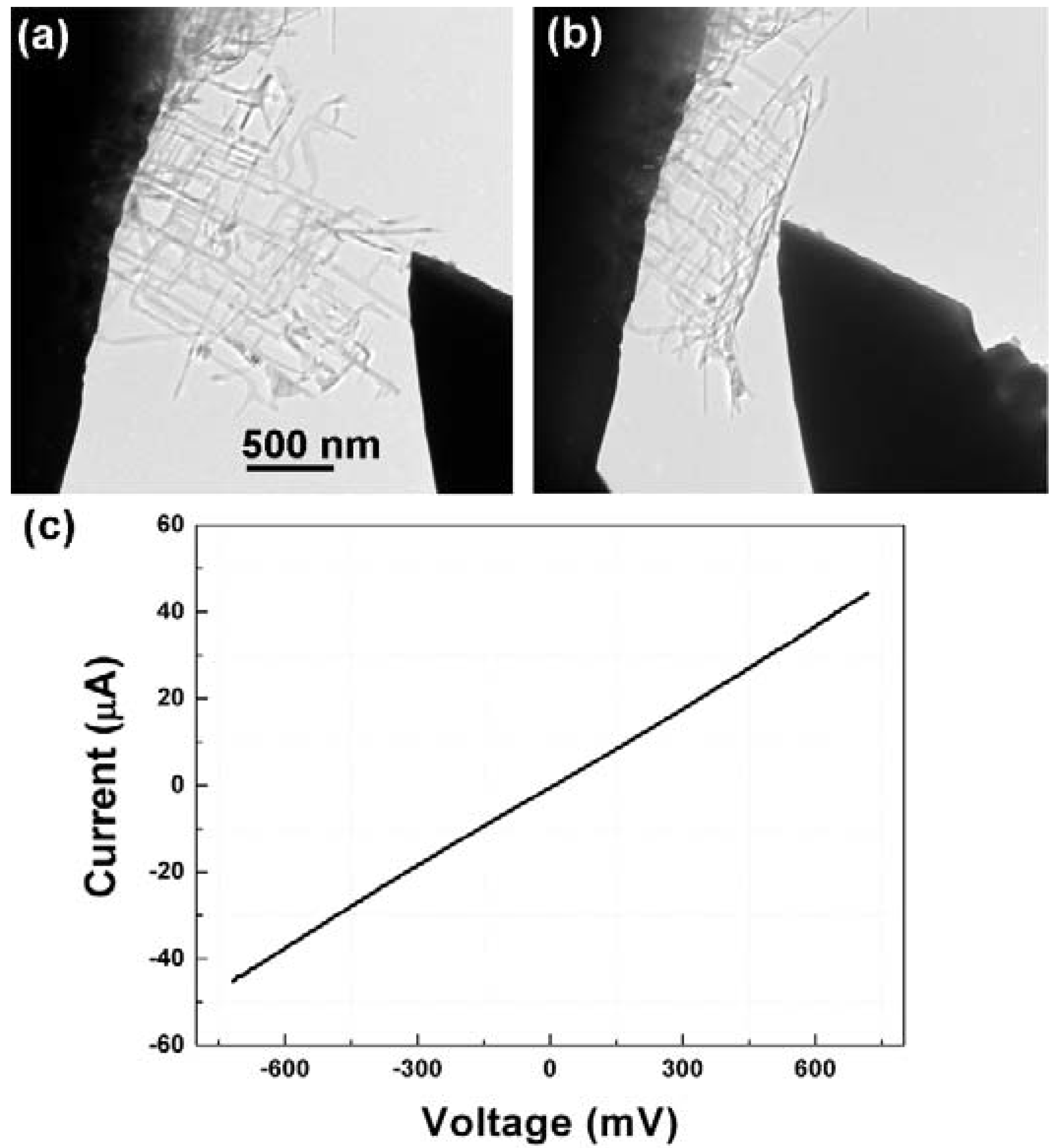
3.1. Hyperbranched nanostructures for hybrid solar cells

One of the chief advantages complex nanostructures exhibit lies in the mechanical strength, which helps maintain the structural integrity when interfaced with other materials such as organic semiconductors. Alivisatos et al. have exploited this aspect by mixing polythiophene (P3HT) and CdSe hyperbranched nanostructures and measured 2.2% efficiencies under AM 1.5 illumination conditions [21]. Although comparable efficiencies have been reported by the same group using CdSe nanostructures with simpler morphologies, such as nanoparticles and nanorods [13], the authors argued that phase segregation during device fabrication is significantly suppressed when hyperbranched nanostructures are used.

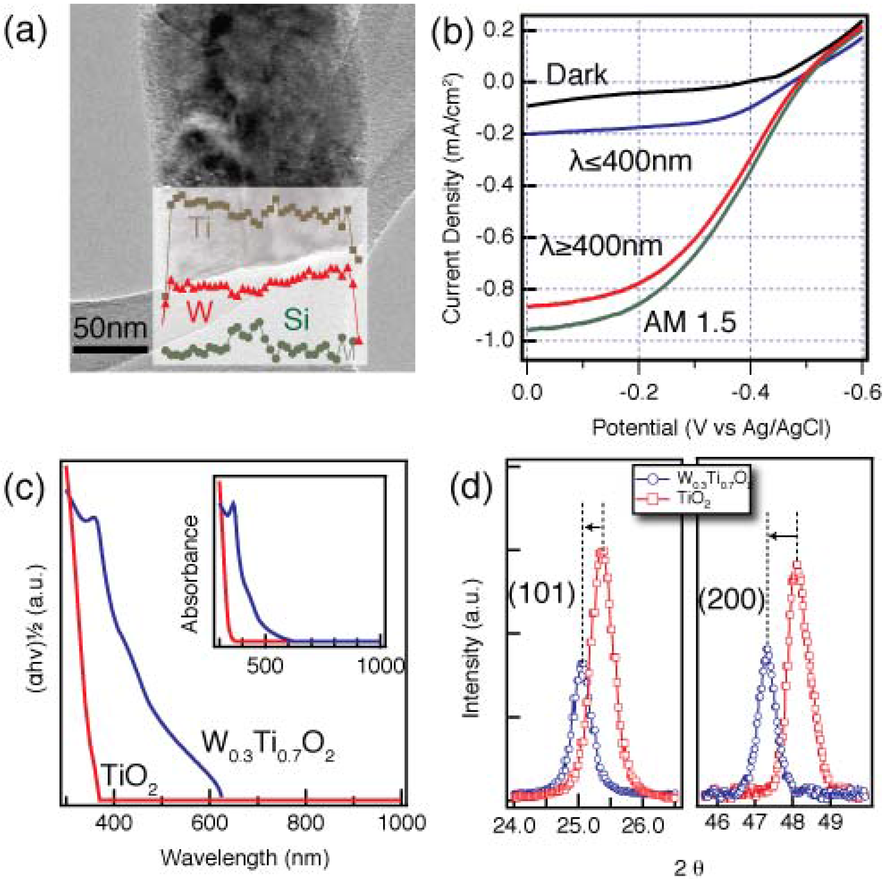
3.2. Complex heterostructures for photoelectrochemical H2O splitting

Similar to the hybrid solar cell applications, the mechanical strength of complex nanostructures may be utilized for photo-to-chemical energy conversion, as well. For this application, high conductivity is another important positive attribute that will help scavenge charges. We exploited this aspect by interfacing highly conductive TiSi2 nanonets with anatase TiO2 and performed water photoelectrolysis experiments [24]. Despite the outstanding chemical stability and excellent catalytic activity, as a photocatalyst TiO2 suffers two major disadvantages: poor conductivity and large bandgap. To improve charge transport while maintaining high surface area, Grimes et al. have used TiO2 nanotubes for water splitting and showed promising results [14,48]. Building upon these results, we took one step further by introducing a component that is solely designed to facilitate charge transport—the highly conductive TiSi2 nanonets.
Figure 8 illustrates this design. In order to achieve high quality TiO2 coating around TiSi2 nanonets, we employed the atomic layer deposition (ALD) method [49]. When immersed in the electrolyte solution, band bending occurs in TiO2 as the equilibrium is established between the solid and the solution. This bending creates a build-in field that serves to separate charges upon photon incidence. Photogenerated electrons are collected by the TiSi2 core while holes go to the solution to oxidize water into O2. Two distinct advantages are offered by our design—the TiO2/electrolyte junction area is maximized, and the charge transport is improved by going through highly conductive TiSi2.
Figure 8. TiO2/TiSi2 heterostructure can be used for water splitting [24]. The structure is schematically shown in (a), which is confirmed by TEM imaging. Reproduced with permissions from American Chemical Society.
Energies 03 00285 g008
Because the photoactive materials are coated onto the TiSi2 scaffold in a separate step, more flexibility can be obtained on tuning the composition or thickness of the active layer. We have doped W into TiO2 and successfully expanded the absorption spectrum to the visible range. Chemical and structural analyses show uniform W0.3Ti0.7O2 coating of the anatase phase was obtained with distorted lattice (Figure 9). The optical bandgap was calculated to be reduced to ~2.0 eV. As a result, improved photocurrent in the visible range was confirmed by the PEC measurements with a peak efficiency of 0.83%. Systematic studies on the composition and structure may optimize the system for a better efficiency of splitting water into clean hydrogen fuel.
Figure 9. One chief advantage of the heterostructure design lies in the flexibility of the shell materials, which is explored here to enhance visible light absorption by doping TiO2 with W [24]. (a) A TEM image of the W0.3Ti0.7O2/TiSi2 heterostructure. Chemical analysis shows uniform doping of tungsten into TiO2 shell. (b) Current-potential plots under different illumination conditions proving photoactivity of the W-doped TiO2 in the visible spectrum. (c) Absorption spectrum showing a reduced band gap of ~2.0 eV from 3.2 eV of pure TiO2. (d) Peak shifts observed in the x-ray diffraction pattern indicate lattice distortion induced by W dopant though the anatase structure is preserved. Reproduced with permissions from American Chemical Society.
Energies 03 00285 g009

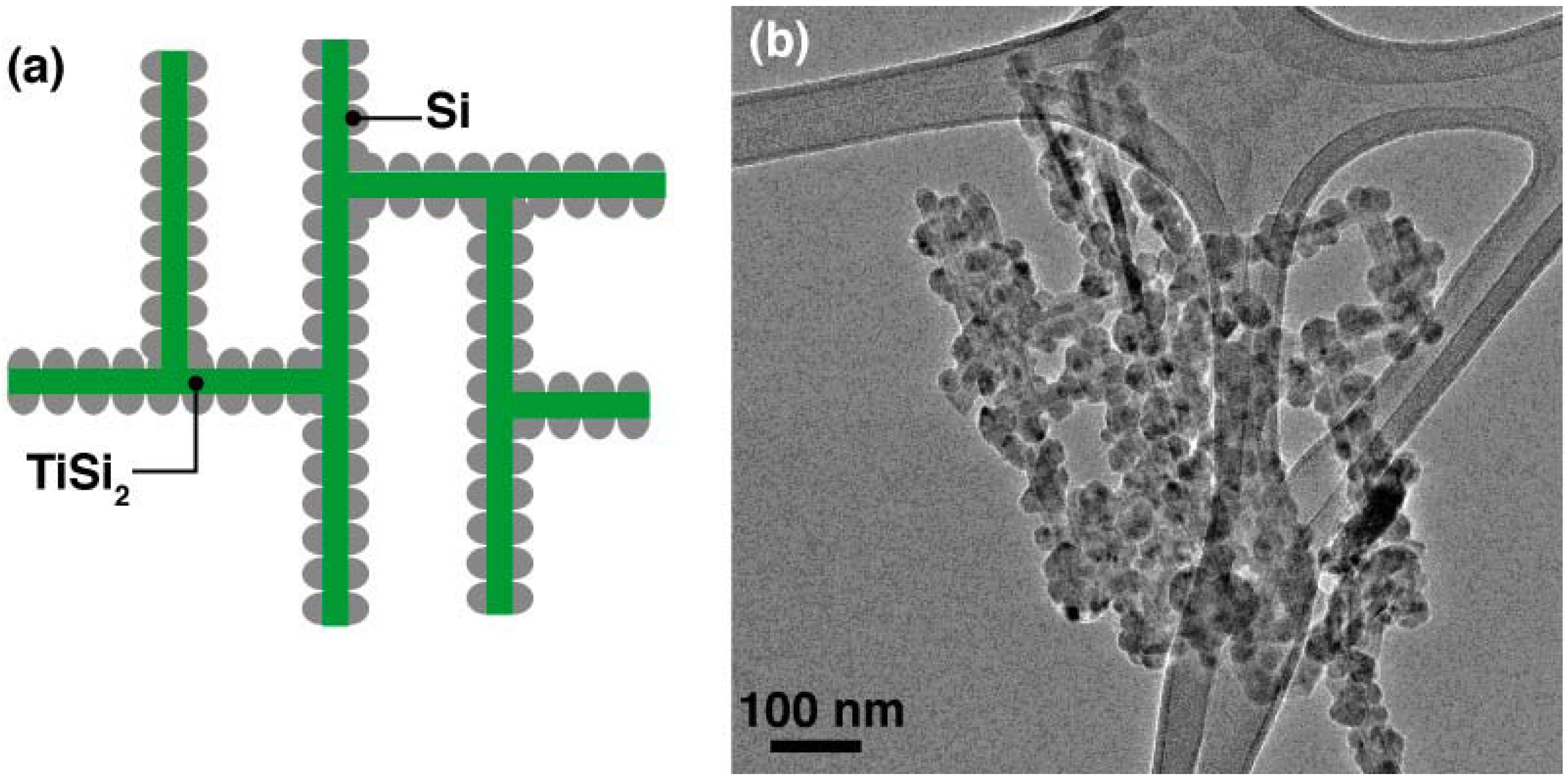
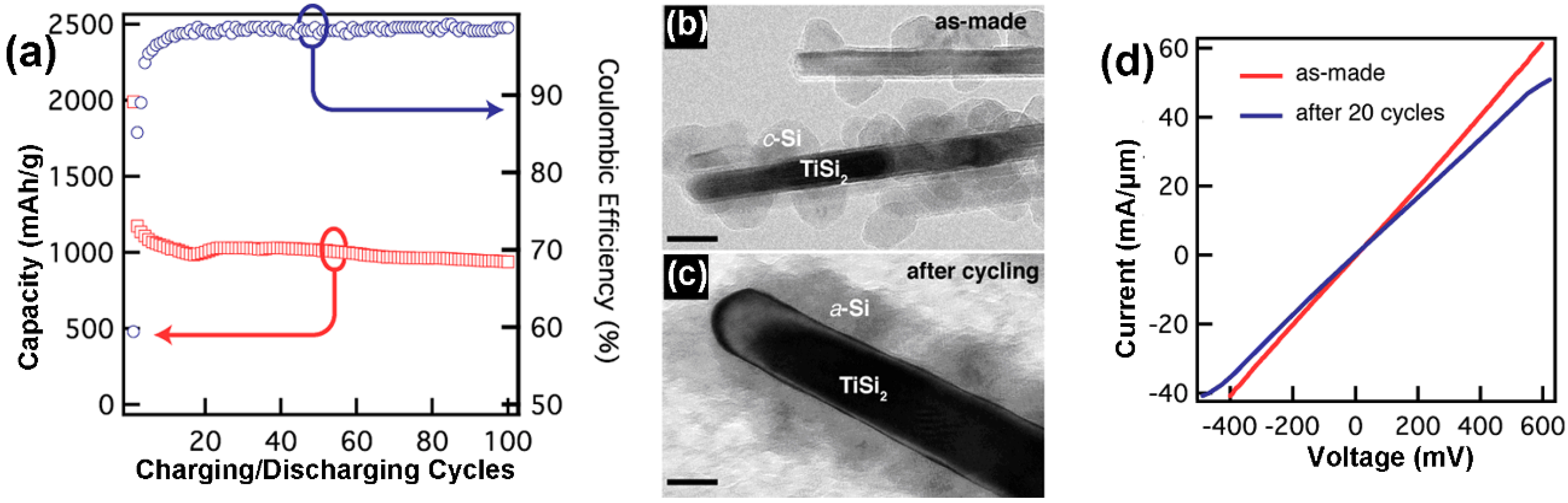
3.3. Si/TiSi2 heterostructures as high-capacity electrode material for rechargeable batteries

The high surface area, good conductivity and strong mechanical strength that complex nanostructures exhibit may also be exploited for electrochemical charge storage. To this end, we have studied combining Si, an appealing high capacity anode material for Li ion batteries, and TiSi2. For this purpose, we coated particulate Si as the active materials on the surface of the TiSi2 nanonets, which serve as the mechanical and electrical support (Figure 10). When proper operation potentials are chosen, Li+ ions are selectively inserted into or extracted from the Si coatings only while the TiSi2 core remains intact. The particulate morphology of the Si coatings provides adequate space to adapt the volume change [26].
Figure 10. Si/TiSi2 heterostructure as anode of a lithium ion battery [26]. (a) A schematic illustration of the design. (b) A TEM image showing particulate Si coated on single-crystalline TiSi2 nanonets. Reproduced with permissions from American Chemical Society.
Energies 03 00285 g010
As shown in Figure 11a, this design produced promising results. The first charging capacity of 1,990 mAh/g was obtained with a charging rate of 8,400 mA/g. During this step, c-Si was converted to a-Si (Figure 11b,c), and the phase transformation resulted in a large drop in the capacity upon discharge to 1,182 mAh/g. Important to the idea, the TiSi2 core remained highly conductive and the morphology was preserved (Figure 11d). The heterostructure showed excellent performance even at high charging/discharging rate. At a fast charging/discharging of 8,400 mA/g, superior capacity retention of >99% per cycle at the level of 1,000 mAh/g over 100 cycles were obtained (Figure 11d).
Figure 11. Performance of Si/TiSi2 heterostructure as anode for Li ion battery [26]. (a) Charge capacity and Coulombic efficiency of the Si/TiSi2 hetero-nanostructure with 8,400 mA/g charge/discharge rate tested between 0.150 and 3.00 V. (b-c) The TiSi2 core remained intact during the test, while the as-made crystalline Si coatings became amorphous after cycling. Scale bars: 20 nm. (d) The electrical conductivity remained high after cycling, further indicating the property of the TiSi2 core was preserved. Reproduced with permissions from American Chemical Society.
Energies 03 00285 g011

4. Conclusions and Prospects

Thanks to their high surface area, strong mechanical strength and superior electronic properties, complex nanostructures are highly desirable for energy applications. When interfaced with another medium, e.g., organic semiconductor or liquid, the fine structures of the complex nanomaterial offer extended interface area, ideal for charge exchange. Once collected, electrons and charges move easily within the complex nanostructure, from one branch to the trunk or to another branch as the components are joined together by high quality crystalline junctions. The crystalline nature of the entire structure also prevents the branches from collapsing, thus helps maintain the high surface area. The ability to efficiently scavenge or deliver electrons and charge are extremely important to applications including solar cells, photoelectrochemical cells and electrochemical storage.
Despite the potentials, complex nanostructures are difficult to synthesize. The anisotropic branches require growth conditions that favor suppressed growth while the complexity of the entire structure demands promoted growth. How to selectively grow branches and join them together represents the main hurdle in producing complex nanostructures. Several approaches utilizing sequential seeding, in situ seeding, phase transition and surface energy differences have been reported and reviewed in this article. Given the promise the complex nanostructures hold, significant efforts to expand these methods or to develop new ones are needed for the synthesis of complex nanostructures with better controls over the morphology and crystal structures.
Although still in its early stage, the science of complex nanostructures has been advanced significantly in the past few years. They have been used to build more efficient solar cells and high-performance photoelectrochemical cells, which converts solar energy directly into electricity and chemicals, respectively. Complex nanostructures have also been shown to work as high capacity electrodes for electrochemical charge storage. The true merit of the reported designs lies in the versatility that different components with distinct functionalities can be readily combined. A new door is opened up to the extended usage of these designs for related energetic applications.

Acknowledgements

The authors thank financial support from Boston College.

References and Notes

  1. Shockley, W.; Queisser, H.J. Detailed balance limit of efficiency of p-n junction solar cells. J. Appl. Phys. 1961, 32, 510–519. [Google Scholar] [CrossRef]
  2. Bolton, J.R. Solar photoproduction of hydrogen: A review. Solar Energy 1996, 57, 37–50. [Google Scholar] [CrossRef]
  3. King, R.R.; Law, D.C.; Edmondson, K.M.; Fetzer, C.M.; Kinsey, G.S.; Yoon, H.; Sherif, R.A.; Karam, N.H. 40% efficient metamorphic GaInP/GaInAs/Ge multijunction solar cells. Appl. Phys. Lett. 2007, 90, 183516. [Google Scholar] [CrossRef]
  4. Lewis, N.S. Powering the planet. Mater. Res. Bull. 2007, 32, 808–820. [Google Scholar] [CrossRef]
  5. Lewis, N.S. Toward cost-effective solar energy use. Science 2007, 315, 798–801. [Google Scholar] [CrossRef] [PubMed]
  6. Nelson, J. The Physics of Solar Cells; Imperial College Press: Longdon, UK, 2003. [Google Scholar]
  7. Miles, R.W.; Zoppi, G.; Forbes, I. Inorganic photovoltaic cells. Mater. Today 2007, 10, 20–27. [Google Scholar] [CrossRef]
  8. Mayer, A.C.; Scully, S.R.; Hardin, B.E.; Rowell, M.W.; McGehee, M.D. Polymer-based solar cells. Mater. Today 2007, 10, 28–33. [Google Scholar] [CrossRef]
  9. Oregan, B.; Gratzel, M. A low-cost, high-efficiency solar-cell based on dye-sensitized colloidal TiO2 films. Nature 1991, 353, 737–740. [Google Scholar] [CrossRef]
  10. Gratzel, M. Dye-sensitized solar cells. J. Photochem. Photobiol., C 2003, 4, 145–153. [Google Scholar] [CrossRef]
  11. Alivisatos, A.P.; Cummings, P.; De Yoreo, J.; Fichthorn, K.; Gates, B.; Hwang, R.; Lowndes, D.; Majumdar, A.; Makowski, L.; Michalske, T.; Misewich, J.; Murray, C.; Sibener, S.; Teague, C.; Williams, E. Nanoscience research for energy needs. In Proceedings of the National Nanotechnology Initiative Grand Challenge Workshop, Alexandria, VA, USA, March 2004.
  12. Greenham, N.C.; Gratzel, M. Nanostructured solar cells. Nanotechnology 2008, 19, 420201. [Google Scholar] [CrossRef]
  13. Huynh, W.U.; Dittmer, J.J.; Alivisatos, A.P. Hybrid nanorod-polymer solar cells. Science 2002, 295, 2425–2427. [Google Scholar] [CrossRef] [PubMed]
  14. Mor, G.K.; Varghese, O.K.; Paulose, M.; Shankar, K.; Grimes, C.A. A review on highly ordered, vertically oriented TiO2 nanotube arrays: Fabrication, material properties, and solar energy applications. Sol. Energy Mater. Sol. Cells 2006, 90, 2011–2075. [Google Scholar] [CrossRef]
  15. Tian, B.; Zheng, X.; Kempa, T.J.; Fang, Y.; Yu, N.; Yu, G.; Huang, J.; Lieber, C.M. Coaxial silicon nanowires as solar cells and nanoelectronic power sources. Nature 2007, 449, 885–889. [Google Scholar] [CrossRef] [PubMed]
  16. Maiolo, J.R.; Kayes, B.M.; Filler, M.A.; Putnam, M.C.; Kelzenberg, M.D.; Atwater, H.A.; Lewis, N.S. High aspect ratio silicon wire array photoelectrochemical cells. J. Am. Chem. Soc. 2007, 129, 12346–12347. [Google Scholar] [CrossRef] [PubMed]
  17. Goodey, A.P.; Eichfeld, S.M.; Lew, K.K.; Redwing, J.M.; Mallouk, T.E. Silicon nanowire array photelectrochemical cells. J. Am. Chem. Soc. 2007, 129, 12344–12345. [Google Scholar] [CrossRef] [PubMed]
  18. Yuhas, B.D.; Yang, P. Nanowire-based all-oxide solar cells. J. Am. Chem. Soc. 2009, 131, 3756–3761. [Google Scholar] [CrossRef] [PubMed]
  19. Manna, L.; Milliron, D.J.; Meisel, A.; Scher, E.C.; Alivisatos, A.P. Controlled growth of tetrapod-branched inorganic nanocrystals. Nat. Mater 2003, 2, 382–385. [Google Scholar] [CrossRef] [PubMed]
  20. Kanaras, A.G.; Sonnichsen, C.; Liu, H.T.; Alivisatos, A.P. Controlled synthesis of hyperbranched inorganic nanocrystals with rich three-dimensional structures. Nano Lett. 2005, 5, 2164–2167. [Google Scholar] [CrossRef] [PubMed]
  21. Gur, I.; Fromer, N.A.; Chen, C.P.; Kanaras, A.G.; Alivisatos, A.P. Hybrid solar cells with prescribed nanoscale morphologies based on hyperbranched semiconductor nanocrystals. Nano Lett. 2007, 7, 409–414. [Google Scholar] [CrossRef] [PubMed]
  22. Wang, D.; Qian, F.; Yang, C.; Zhong, Z.H.; Lieber, C.M. Rational growth of branched and hyperbranched nanowire structures. Nano Lett. 2004, 4, 871–874. [Google Scholar] [CrossRef]
  23. Zhou, S.; Liu, X.H.; Lin, Y.J.; Wang, D.W. Spontaneous growth of highly conductive two-dimensional TiSi2 nanonets. Angew. Chem. Int. Ed. 2008, 47, 7681–7684. [Google Scholar] [CrossRef]
  24. Lin, Y.; Zhou, S.; Liu, X.; Sheehan, S.; Wang, D. TiO2/TiSi2 heterostructures for high-efficiency photoelectrochemical H2O splitting. J. Am. Chem. Soc. 2009, 131, 2772–2773. [Google Scholar] [CrossRef] [PubMed]
  25. Zhou, S.; Liu, X.; Lin, Y.; Wang, D. Rational synthesis and structural characterizations of complex TiSi2 nanostructures. Chem. Mater. 2009, 21, 1023–1027. [Google Scholar] [CrossRef]
  26. Zhou, S.; Liu, X.H.; Wang, D.W. Si/TiSi2 Hetero-nanostructures as anode material for Li ion batteries. Nano Lett. 2010. [Google Scholar] [CrossRef]
  27. Wagner, R.S.; Ellis, W.C. Vapor-liquid-solid mechanism of single crystal growth. Appl. Phys. Lett. 1964, 4, 89–90. [Google Scholar] [CrossRef]
  28. Dick, K.A.; Deppert, K.; Larsson, M.W.; Martensson, T.; Seifert, W.; Wallenberg, L.R.; Samuelson, L. Synthesis of branched 'nanotrees' by controlled seeding of multiple branching events. Nat. Mater. 2004, 3, 380–384. [Google Scholar] [CrossRef] [PubMed]
  29. Zhu, J.; Peng, H.L.; Chan, C.K.; Jarausch, K.; Zhang, X.F.; Cui, Y. Hyperbranched lead selenide nanowire networks. Nano Lett. 2007, 7, 1095–1099. [Google Scholar] [CrossRef] [PubMed]
  30. Dick, K.A.; Deppert, K.; Karlsson, L.S.; Seifert, W.; Wallenberg, L.R.; Samuelson, L. Position-controlled interconnected InAs nanowire networks. Nano Lett. 2006, 6, 2842–2847. [Google Scholar] [CrossRef] [PubMed]
  31. Wan, Q.; Wei, M.; Zhi, D.; MacManus-Driscoll, J.L.; Blamire, M.G. Epitaxial growth of vertically aligned and branched single-crystalline Tin-doped indium oxide nanowire arrays. Adv. Mater. 2006, 18, 234–238. [Google Scholar] [CrossRef]
  32. Cheng, C.; Liu, B.; Yang, H.; Zhou, W.; Sun, L.; Chen, R.; Yu, S.F.; Zhang, J.; Gong, H.; Sun, H.; Fan, H.J. Hierarchical assembly of ZnO nanostructures on SnO2 backbone nanowires: Low-temperature hydrothermal preparation and optical properties. ACS Nano 2009, 3, 3069–3076. [Google Scholar] [CrossRef] [PubMed]
  33. Lao, J.Y.; Wen, J.G.; Ren, Z.F. Hierarchical ZnO nanostructures. Nano Lett. 2002, 2, 1287–1291. [Google Scholar] [CrossRef]
  34. Jung, Y.; Ko, D.K.; Agarwal, R. Synthesis and structural characterization of single-crystalline branched nanowire heterostructures. Nano Lett. 2007, 7, 264–268. [Google Scholar] [CrossRef] [PubMed]
  35. Wan, Q.; Dattoli, E.N.; Fung, W.Y.; Guo, W.; Chen, Y.; Pan, X.; Lu, W. High-performance transparent conducting oxide nanowires. Nano Lett. 2006, 6, 2909–2915. [Google Scholar] [CrossRef] [PubMed]
  36. Cao, A.Y.; Veedu, V.P.; Li, X.S.; Yao, Z.L.; Ghasemi-Nejhad, M.N.; Ajayan, P.M. Multifunctional brushes made from carbon nanotubes. Nat. Mater. 2005, 4, 540–545. [Google Scholar] [CrossRef] [PubMed]
  37. Bierman, M.J.; Lau, Y.K.A.; Jin, S. Hyperbranched PbS and PbSe nanowires and the effect of hydrogen gas on their synthesis. Nano Lett. 2007, 7, 2907–2912. [Google Scholar] [CrossRef] [PubMed]
  38. Lao, J.Y.; Huang, J.Y.; Wang, D.Z.; Ren, Z.F. ZnO nanobridges and nanonails. Nano Lett. 2003, 3, 235–238. [Google Scholar] [CrossRef]
  39. Bierman, M.J.; Lau, Y.K.A.; Kvit, A.V.; Schmitt, A.L.; Jin, S. Dislocation-driven nanowire growth and eshelby twist. Science 2008, 320, 1060–1063. [Google Scholar] [CrossRef] [PubMed]
  40. Lau, Y.K.A.; Chernak, D.J.; Bierman, M.J.; Jin, S. Formation of PbS nanowire pine trees driven by screw dislocations. J. Am. Chem. Soc. 2009, 131, 16461–16471. [Google Scholar] [CrossRef] [PubMed]
  41. Bierman, M.J.; Lau, Y.K.A.; Jin, S. Hyperbranched PbS and PbSe nanowires and the effect of hydrogen gas on their synthesis. Nano Lett. 2007, 7, 2907–2912. [Google Scholar] [CrossRef] [PubMed]
  42. Wang, D.L.; Lieber, C.M. Inorganic materials: Nanocrystals branch out. Nat. Mater. 2003, 2, 355–356. [Google Scholar] [CrossRef] [PubMed]
  43. Milliron, D.J.; Hughes, S.M.; Cui, Y.; Manna, L.; Li, J.B.; Wang, L.W.; Alivisatos, A.P. Colloidal nanocrystal heterostructures with linear and branched topology. Nature 2004, 430, 190–195. [Google Scholar] [CrossRef] [PubMed]
  44. Ding, Y.; Wang, Z.L.; Sun, T.J.; Qiu, J.S. Zinc-blende ZnO and its role in nucleating wurtzite tetrapods and twinned nanowires. Appl. Phys. Lett. 2007, 90, 153510. [Google Scholar] [CrossRef]
  45. Beyers, R.; Sinclair, R. Metastable phase formation in titanium-silicon thin films. J. Appl. Phys. 1985, 57, 5240–5245. [Google Scholar] [CrossRef]
  46. Murarka, S.P.; Fraser, D.B.; Sinha, A.K.; Levinstein, H.J. Refractory silicides of titanium and tantalum for low-resistivity gates and interconnects. IEEE Trans. Electron. Devices 1980, 27, 1409–1417. [Google Scholar] [CrossRef]
  47. Ekman, M.; Ozolins, V. Electronic structure and bonding properties of titanium silicides. Phys. Rev. B: Condens. Matter 1998, 57, 4419. [Google Scholar] [CrossRef]
  48. Mor, G.K.; Shankar, K.; Paulose, M.; Varghese, O.K.; Grimes, C.A. Enhanced photocleavage of water using titania nanotube arrays. Nano Lett. 2005, 5, 191–195. [Google Scholar] [CrossRef] [PubMed]
  49. Pore, V.; Rahtu, A.; Leskela, M.; Ritala, M.; Sajavaara, D.; Keinonen, J. Atomic layer deposition of photocatalytic TiO2 thin films from titanium tetramethoxide and water. Chem. Vapor Deposition 2004, 10, 143–148. [Google Scholar] [CrossRef]

