Analysis of a Single-Phase Z-Source Inverter for Battery Discharging in Vehicle to Grid Applications

Abstract
:1. Introduction

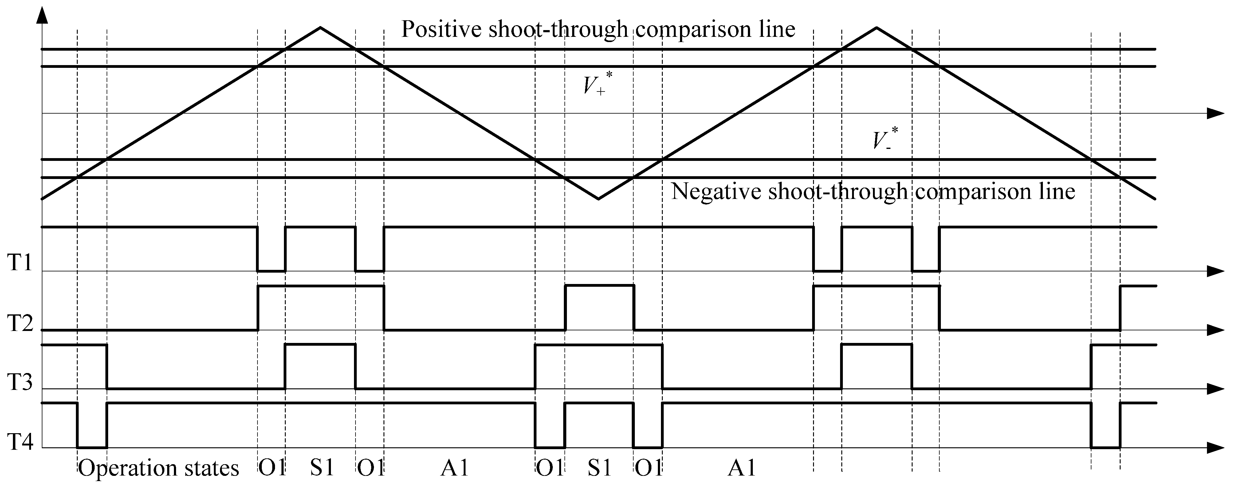
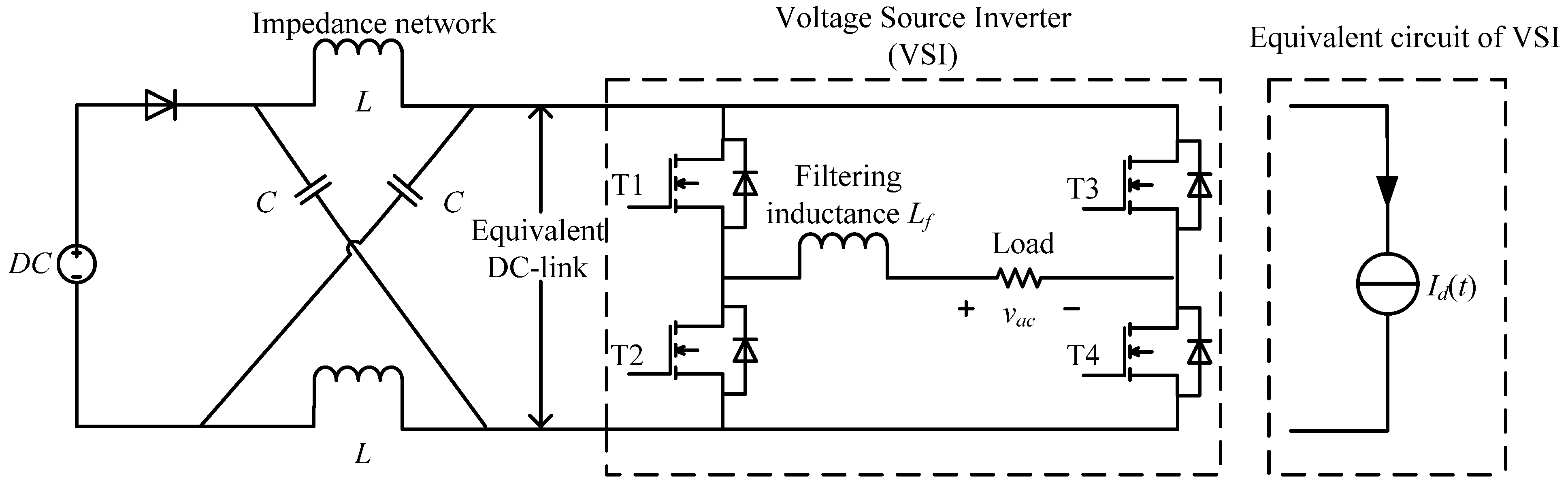
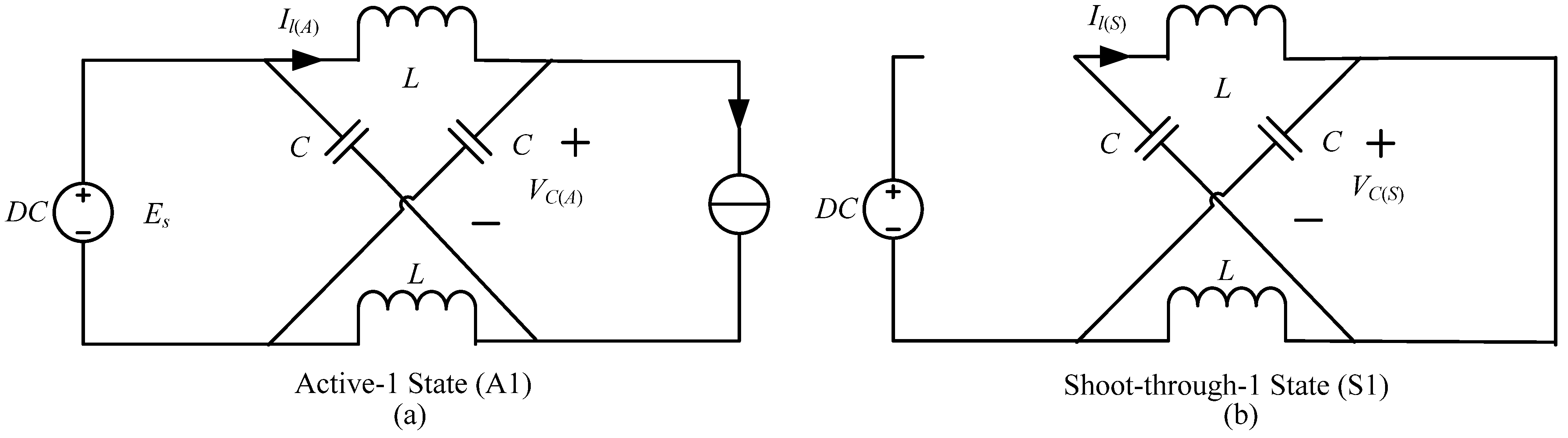
2. DC Side Current of Single-Phase ZSI


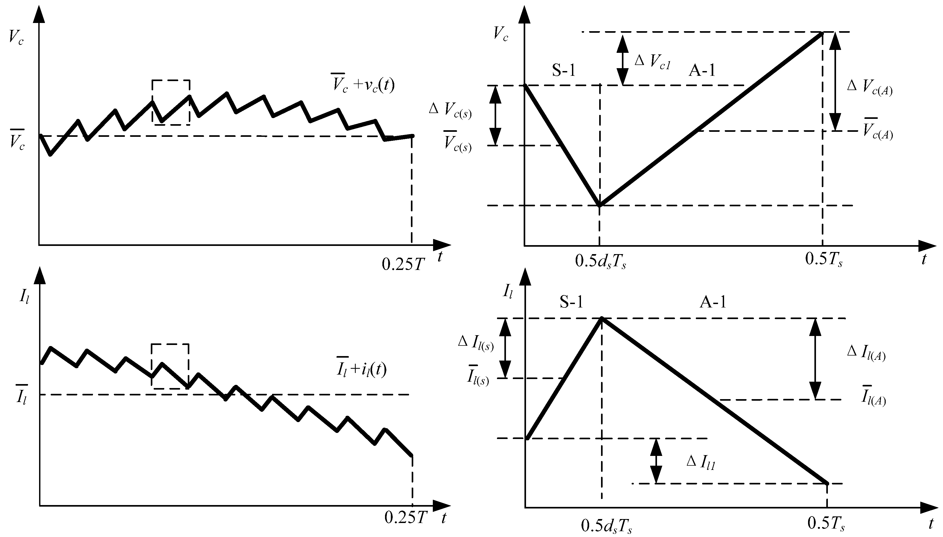
3. High-Frequency Ripple Analysis of Single-Phase ZSI


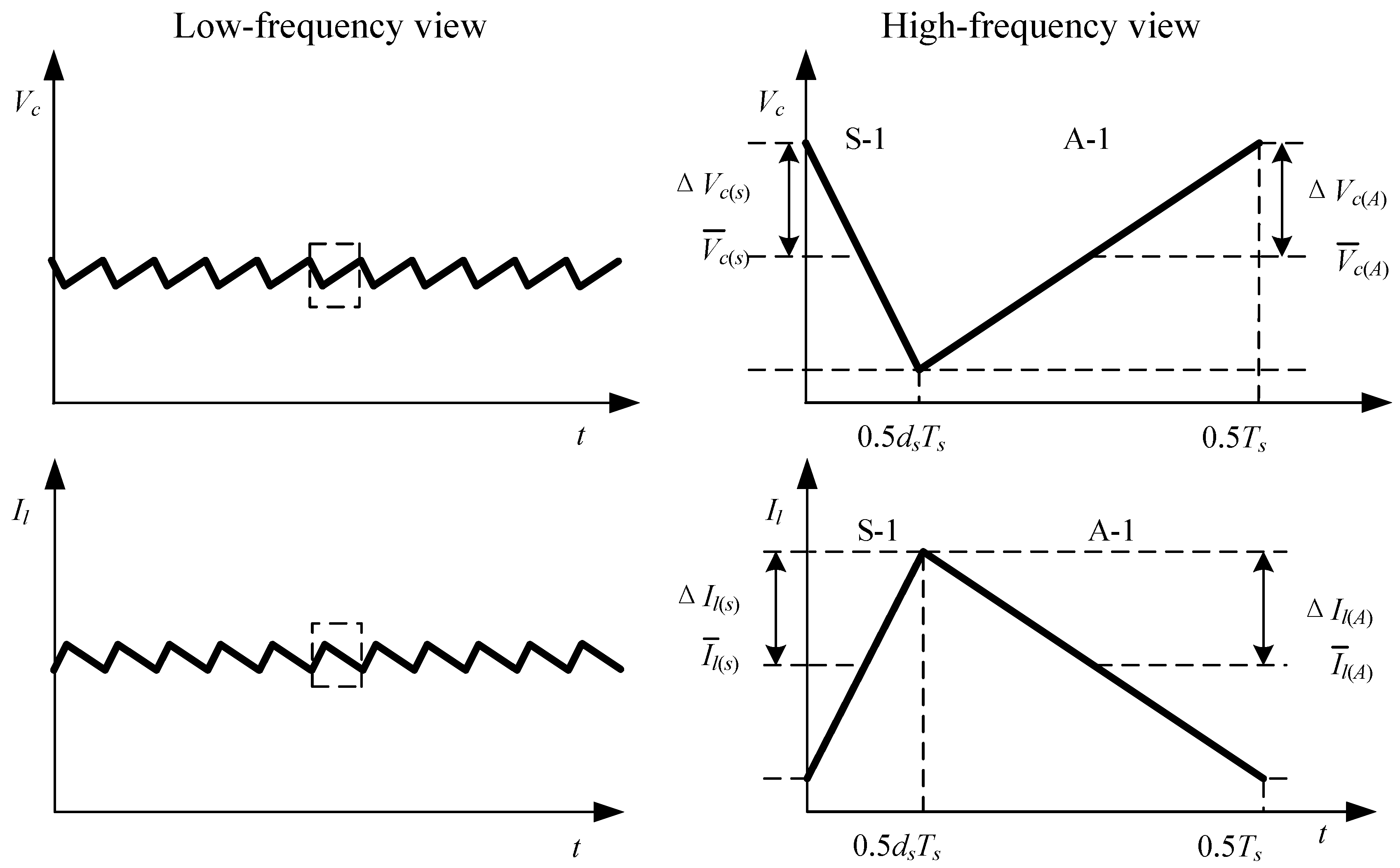


 (refer to Figure 3a). Therefore, high-frequency ripple factor of DC-link voltage:

4. Low-Frequency Ripple Analysis of Single-Phase ZSI


 and
and  yields:


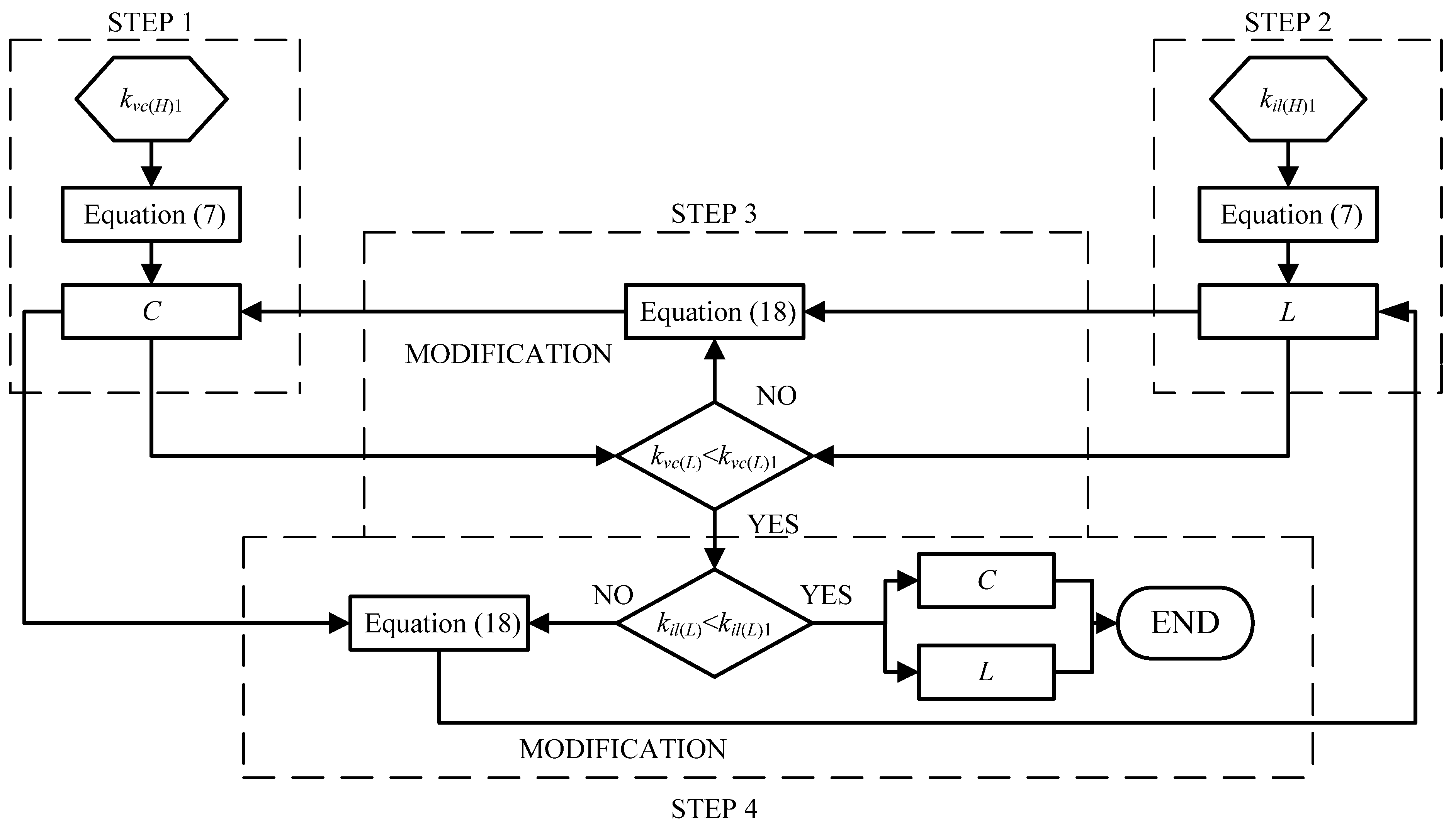
5. Z-Source Network Design Approach
- ■
- targeted high-frequency capacitor voltage ripple factor kvc(H)1
- ■
- targeted high-frequency inductor current ripple factor kil(H)1
- ■
- targeted low-frequency capacitor voltage ripple factor kvc(L)1
- ■
- targeted low-frequency inductor current ripple factor kil(L)1
- (1)
- calculating C based on kvc(H)1 constraint
- (2)
- calculating L based on kil(H)1 constraint
- (3)
- checking whether kvc(L)1 constraint is met, modifying C if not
- (5)
- checking whether kil(L)1 constraint is met, modifying L if not


| Output Voltage/Frequency | DC Source (Es) | Load Resistance/Inductance | Carrier Frequency (fs) | Shoot-through Duty Ratio (ds) | Modulation Index (M) |
|---|---|---|---|---|---|
| 55 V/50 Hz | 70 V | 10 Ω/2 mH | 10 kHz | 0.1 | 0.8889 |
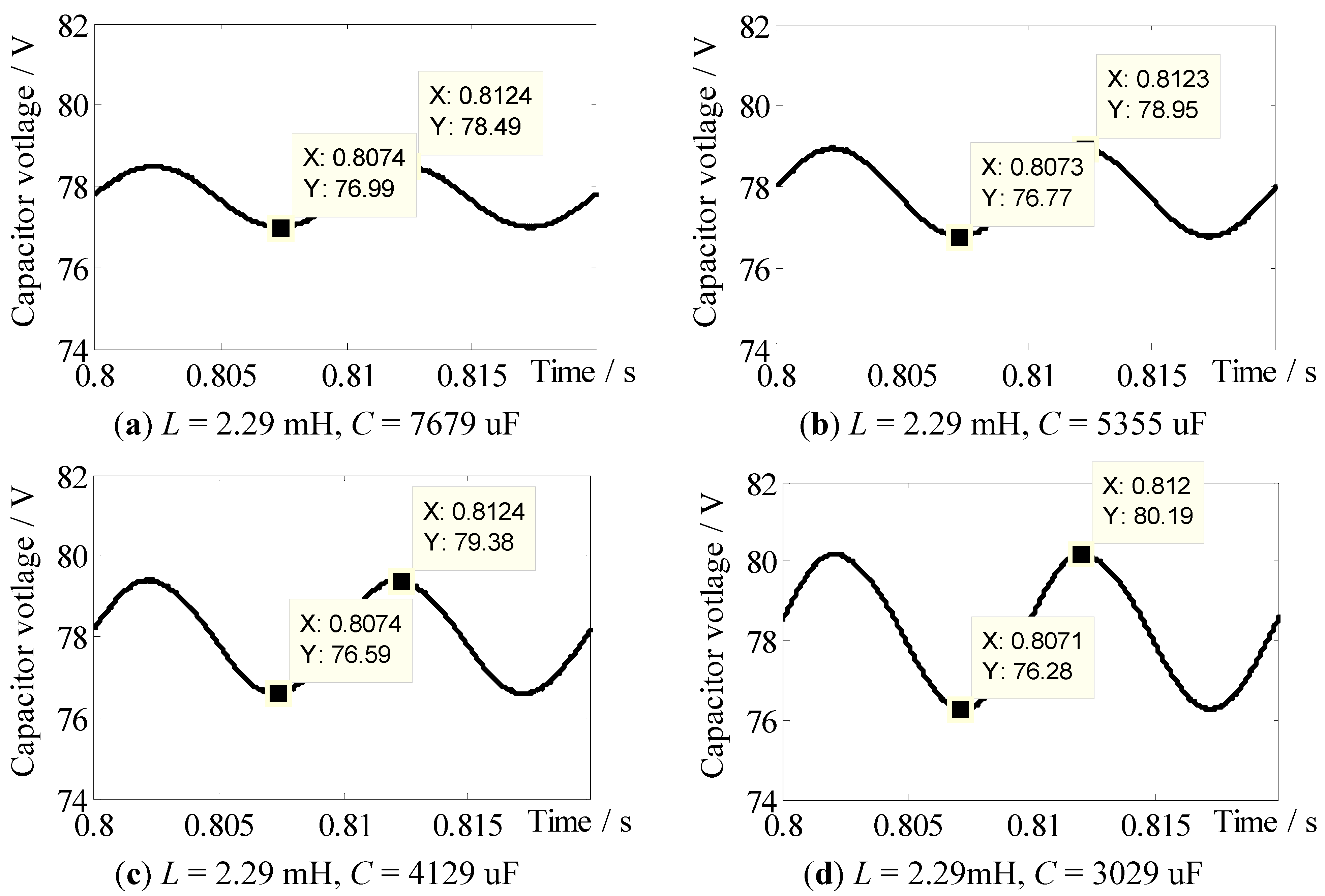
| Design Input | Design Output | Simulation Comparison | |||||
|---|---|---|---|---|---|---|---|
| kvc(H)1 | kil(H)1 | kil(L)1 | kvc(L)1 | (kv(L)) | L/mH | C/uF | kvc(L) |
| 2% | 2% | 10% | 1.00% | (1.80%) | 2.29 | 7679 | 0.96% |
| 1.50% | (2.70%) | 2.29 | 5355 | 1.40% | |||
| 2.00% | (3.60%) | 2.29 | 4192 | 1.79% | |||
| 3.00% | (5.40%) | 2.29 | 3029 | 2.50% | |||
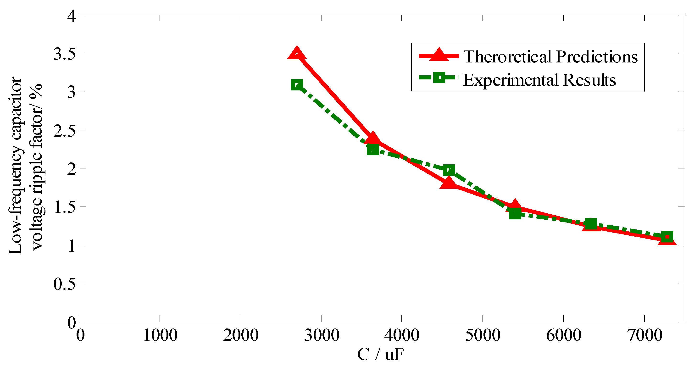
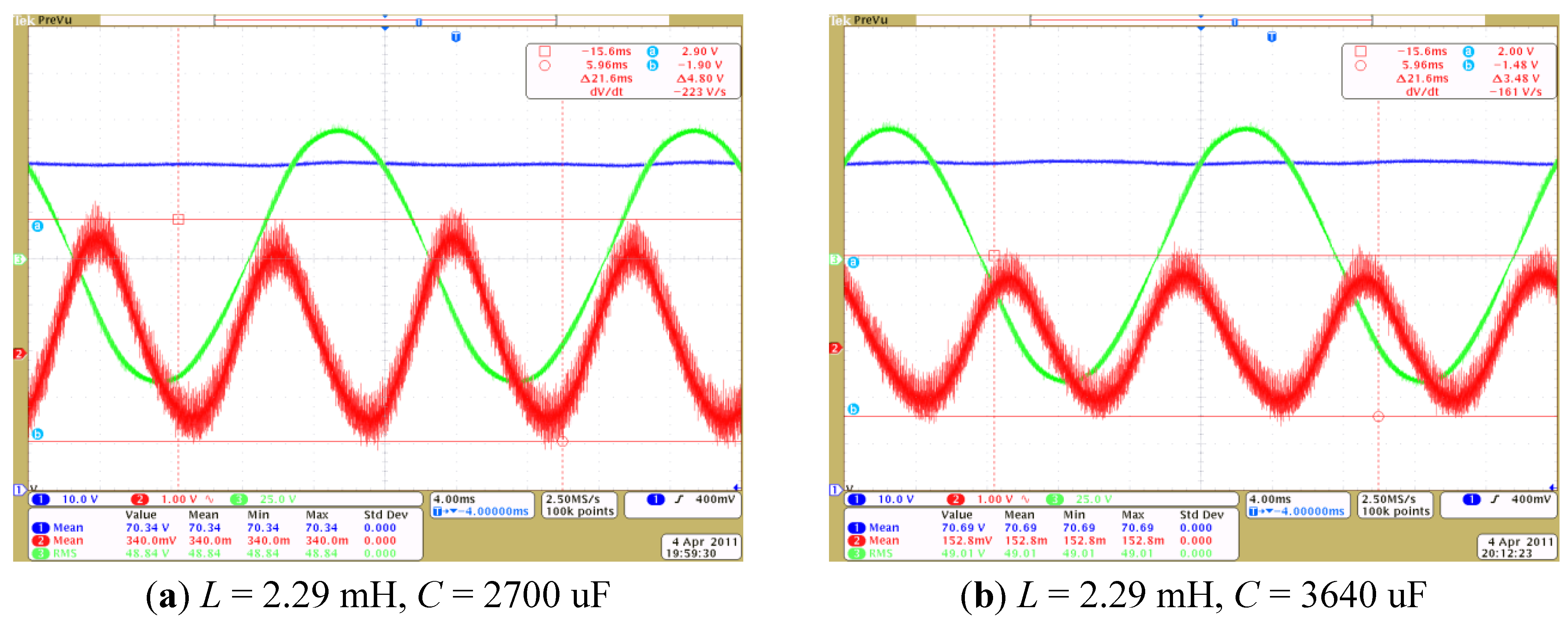
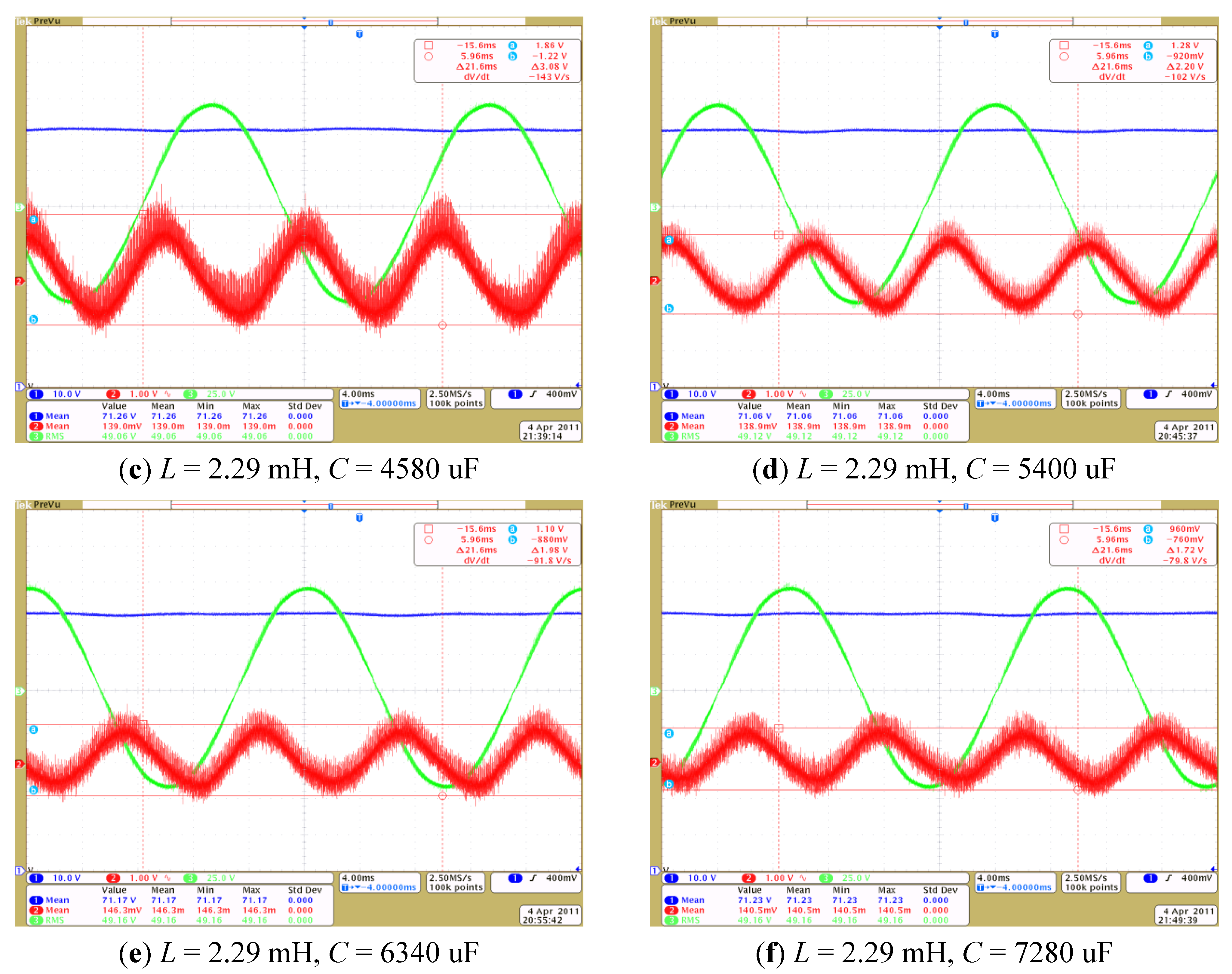
6. Experimental Verification

| Z-Source Network Parameters | Low-Frequency Capacitor Voltage Ripple Factor kvc(L) | ||
|---|---|---|---|
| L/mH | C/uF | Theoretical Predictions | Experimental Results |
| 2.29 | 2700 | 3.49% | 3.09% |
| 2.29 | 3640 | 2.38% | 2.24% |
| 2.29 | 4580 | 1.80% | 1.97% |
| 2.29 | 5400 | 1.49% | 1.41% |
| 2.29 | 6340 | 1.24% | 1.27% |
| 2.29 | 7280 | 1.06% | 1.10% |


7. Conclusions
Acknowledgments
References
- Madawala, U.K.; Thrimawithana, D.J. A bidirectional inductive power interface for electric vehicles in V2G systems. IEEE Trans. Ind. Electron. 2011, 58, 4789–4796. [Google Scholar] [CrossRef]
- Peng, F.Z. Z-Source Inverter. IEEE Trans. Ind. Appl. 2003, 39, 504–510. [Google Scholar] [CrossRef]
- Peng, F.Z.; Shen, M.; Qian, Z. Maximum boost control of the Z-Source inverter. IEEE Trans. Power Electron. 2005, 20, 833–838. [Google Scholar] [CrossRef]
- Shen, M.; Wang, J.; Joseph, A.; Peng, F.Z.; Tolbert, L.M.; Adams, D.J. Constant boost control of the Z-Source inverter to minimize current ripple and voltage stress. IEEE Trans. Ind. Appl. 2006, 42, 770–778. [Google Scholar] [CrossRef]
- Yang, S.; Ding, X.; Peng, F.Z.; Qian, Z. Unified Control Technique for Z-Source Inverter. In Proceedings of the 39th IEEE Annual Power Electronics Specialists Conference, Rhodes, Greece, 15–19 June 2008; pp. 3236–3242.
- Liu, J.; Hu, J.; Xu, L. Dynamic modeling and analysis of Z source converter: Derivation of AC small signal model and design-oriented analysis. IEEE Trans. Power Electron. 2007, 22, 1786–1796. [Google Scholar] [CrossRef]
- Tang, Y.; Xie, S.; Zhang, C.; Xu, Z. Improved Z-Source inverter with reduced Z-source capacitor voltage stress and soft-start capability. IEEE Trans. Power Electron. 2009, 24, 409–415. [Google Scholar] [CrossRef]
- Anderson, J.; Peng, F.Z. Four Quasi-Z-Source Inverters. In Proceedings of the 39th IEEE Annual Power Electronics Specialists Conference, Rhodes, Greece, 15–19 June 2008; pp. 2743–2749.
- Li, Y.; Anderson, J.; Peng, F.Z.; Liu, D. Quasi-Z-Source Inverter for Photovoltaic Power Generation Systems. In Proceedings of the 25th Annual IEEE Applied Power Electronics Conference and Exposition, Palm Springs, CA, USA, 21–25 February 2009; pp. 918–924.
- Ding, X.; Qian, Z.; Yang, S.; Cui, B.; Peng, F.Z. A New Adjustable-Speed Drives (ASD) System Based on High-Performance Z-Source Inverter. In Proceedings of the 42th IEEE Annual Industrial Application Society Meeting, New Orleans, LA, USA, 23–27 September 2007; pp. 2327–2332.
- Zhou, Z.J.; Zhang, X.; Xu, P.; Shen, W.X. Single-phase uninterruptible power supply based on Z-source inverter. IEEE Trans. Ind. Electron. 2008, 55, 2997–3004. [Google Scholar] [CrossRef]
- Rajakaruna, S.; Jayawickrama, L. Steady-state analysis and designing impedance network of Z-source inverters. IEEE Trans. Ind. Electron. 2010, 57, 2483–2491. [Google Scholar] [CrossRef]
© 2011 by the authors; licensee MDPI, Basel, Switzerland. This article is an open access article distributed under the terms and conditions of the Creative Commons Attribution license (http://creativecommons.org/licenses/by/3.0/).
Share and Cite
Yu, Y.; Zhang, Q.; Liang, B.; Liu, X.; Cui, S. Analysis of a Single-Phase Z-Source Inverter for Battery Discharging in Vehicle to Grid Applications. Energies 2011, 4, 2224-2235. https://doi.org/10.3390/en4122224
Yu Y, Zhang Q, Liang B, Liu X, Cui S. Analysis of a Single-Phase Z-Source Inverter for Battery Discharging in Vehicle to Grid Applications. Energies. 2011; 4(12):2224-2235. https://doi.org/10.3390/en4122224
Chicago/Turabian StyleYu, Yifan, Qianfan Zhang, Bin Liang, Xiaofei Liu, and Shumei Cui. 2011. "Analysis of a Single-Phase Z-Source Inverter for Battery Discharging in Vehicle to Grid Applications" Energies 4, no. 12: 2224-2235. https://doi.org/10.3390/en4122224