1. Introduction
The liberalization of the electricity market and the environmental concerns associated with greenhouse gas emissions, have given significant momentum to the diffusion of distributed generation units (DGUs) [
1]. The growing number of DGUs has changed the traditional operations of distribution grids from passive networks to microgrids.
Typical microsources, e.g., microturbines, photovoltaic panels, and fuel cells, have small power (<100 kW) with power electronics interfaces and are placed at customers’ sites. Power electronics provide microgrids with the flexibility of operation required by the customers. This flexibility is exploited by a suitable control of the power flows in the different sections of the microgrids. The controller regulates the power flow at the connection point to the level prescribed by the energy manager of the utility grid. As loads downstream change, local microsources increase or decrease their power output to hold the power flow constant. Renewable energy sources (RES) are usually equipped with maximum power point tracking controllers and, hence, the generation of electricity is dependent on weather conditions rather than on customers’ needs. Electric storage devices can compensate for the mismatch between the power generated and that consumed by the loads, keeping the desired value of the power flow at the connection point [
2].
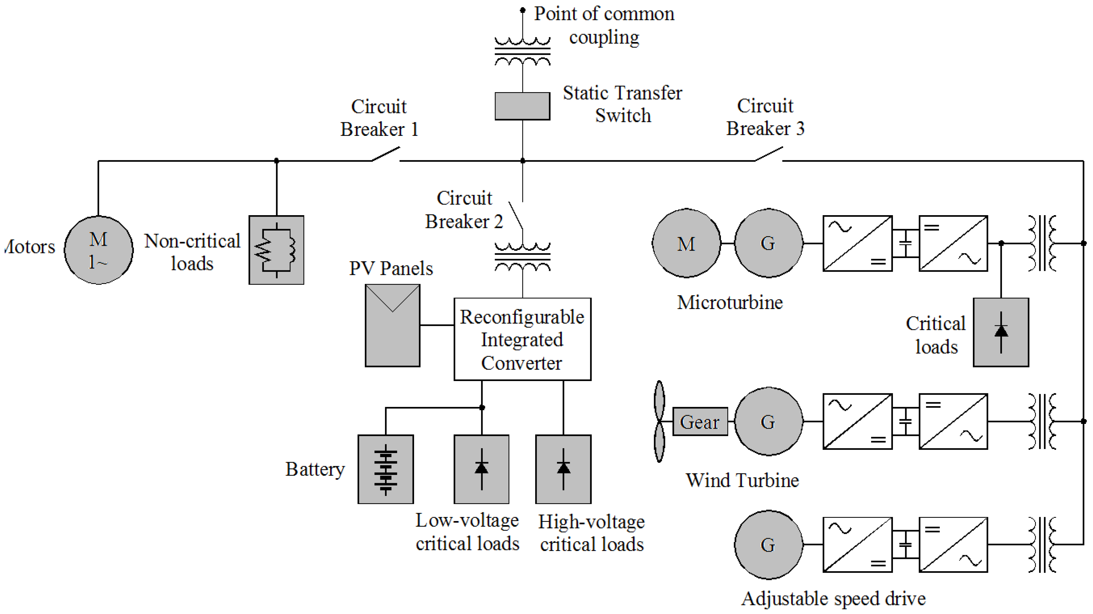
The typical configuration of a grid interactive Alternating Current AC microgrid is illustrated in
Figure 1 [
3]. On the basis of the connection to the microgrid, DGUs are distinguished between conventional rotary units and electronically coupled units.
Figure 1.
Configuration of a typical AC microgrid.
Figure 1.
Configuration of a typical AC microgrid.
Conventional rotary units, which include fixed speed wind turbines, gas microturbines, internal combustion engines and small hydro turbines, are interfaced directly through the rotating generators [
4]. Electronically coupled DGUs,
i.e., variable speed wind turbines, photovoltaic arrays and fuel cells, are connected to the microgrid by means of power electronics converters that play a central role then fault-tolerant characteristics are requested [
5]. Energy storage devices are also electronically coupled to the microgrid, due to the need of regulating their charge and discharge rates.
DGUs based on renewable energy sources need a conversion system to tie into the AC grid. Very often this power is reconverted again to DC for many end uses. In fact, all the electronic devices, such as computers, florescent lights, variable speed drives and many other household and business appliances and equipment, need DC supply, hence all of these DC devices require conversion of the building’s AC power into DC and this conversion is typically made by inefficient rectifiers. The power losses of these multiple conversions could be reduced using DC microgrids,
i.e., DC grids within the buildings or group of several buildings. In this type of microgrid, AC mains power is converted to DC using an efficient rectifier; the DC network then supplies power to DC equipment connected to the DC network itself. With reference to
Figure 1, the block “Reconfigurable integrated converter” is the interface between the AC power and the DC microgrid, which can have also different DC voltage levels. Potentially, a DC microgrid can reduce AC to DC conversion losses from an average of 32% to 10% [
6,
7]. In addition, rooftop photovoltaic and other distributed DC sources can supply power directly to DC equipment without the need of a double stage converter or a bulky transformer.
Power supplies currently on the market have a minimum efficiency of between 60% and 85%. This efficiency could be readily raised to 85%–90% in a DC microgrid by using high efficiency centralized DC-DC converters. This configuration, based on a bulk conversion, is likely to be also cheaper than that based on a converter at every point-of-use. These power converters should be the flexible interface between DC sources, DC loads, DC storage devices and AC mains, adapting on the different conditions of the grid and the customers’ requirements. Reconfigurable integrated converters (RIC) are the best candidates to meet the requirements of flexibility and capability of managing the power flows between multiple electrical circuits at different voltages and frequencies. This paper analyses a RIC used for a domestic microgrid with inputs from the AC mains and photovoltaic arrays, and two DC outputs at different voltage levels. RIC can change its configuration upon the needs of the microgrid using the same hardware, i.e., semiconductor switches, magnetics and capacitors, and different control strategies based on a hierarchic logic. The high-level logic defines the converter configuration and arranges the power circuit accordingly. The mid-level logic manages the control of the converter for the specific configuration selected on the basis of the references generated for the desired targets. The low-level logic achieves the switching of the components and the measurement of the field variables.
Starting from the traditional single-input single-output DC/DC converter topology, a RIC converter can be configured in a single-input dual-output mode, using a different number of components in comparison with two traditional choppers. Some multi-output solution use one controllable component for charging the input inductor and a number of switches correspondent to the number of outputs [
8,
9,
10]; this leads to three switches for dual-output configuration. Some other topologies are provided with even more components (switches and diode) [
11], and solutions with a multi-windings transformer have also been proposed [
12,
13]. This paper focuses on the analysis of the RIC as a dual-boost DC-DC converter. Compared with some other solutions, the structure proposed in this paper operates with reduced number of components and no multi-windings transformers are used. This contributes to the compactness and the simplicity of the converter, with benefits in terms of lost power. Simulations results give evidence on the controllability of this converter and the capability of achieving the desired voltage outputs with reduced ripple.
2. The Reconfigurable Integrated Converter (RIC)
According to the DC microgrid basics, the structure is based on a local distribution DC grid. Moreover an AC bus is also considered to supply power to traditional AC loads. A proposed high voltage DC bus (200 V)—is used to provide energy for heavy DC loads—for example household electrical appliances—while a low voltage DC bus (48 V)—provides energy to the consumer electronics. This architecture makes easier to distribute the DC power generated by the renewable energy sources and stored in the batteries.
The power electronics interface (PEI) is the interface between renewable electrical sources, the AC mains and the loads. Moreover, PEI adapts the power generated to the load demand in terms of supply type—AC or DC—and voltage level. PEI generally includes several converter modules, though not every module is always in operation. Therefore, the introduction of integrated topologies, capable of achieving different conversion functions, could lead to equipment cost significant cheaper without affecting the requirements of both users and the utility grid.
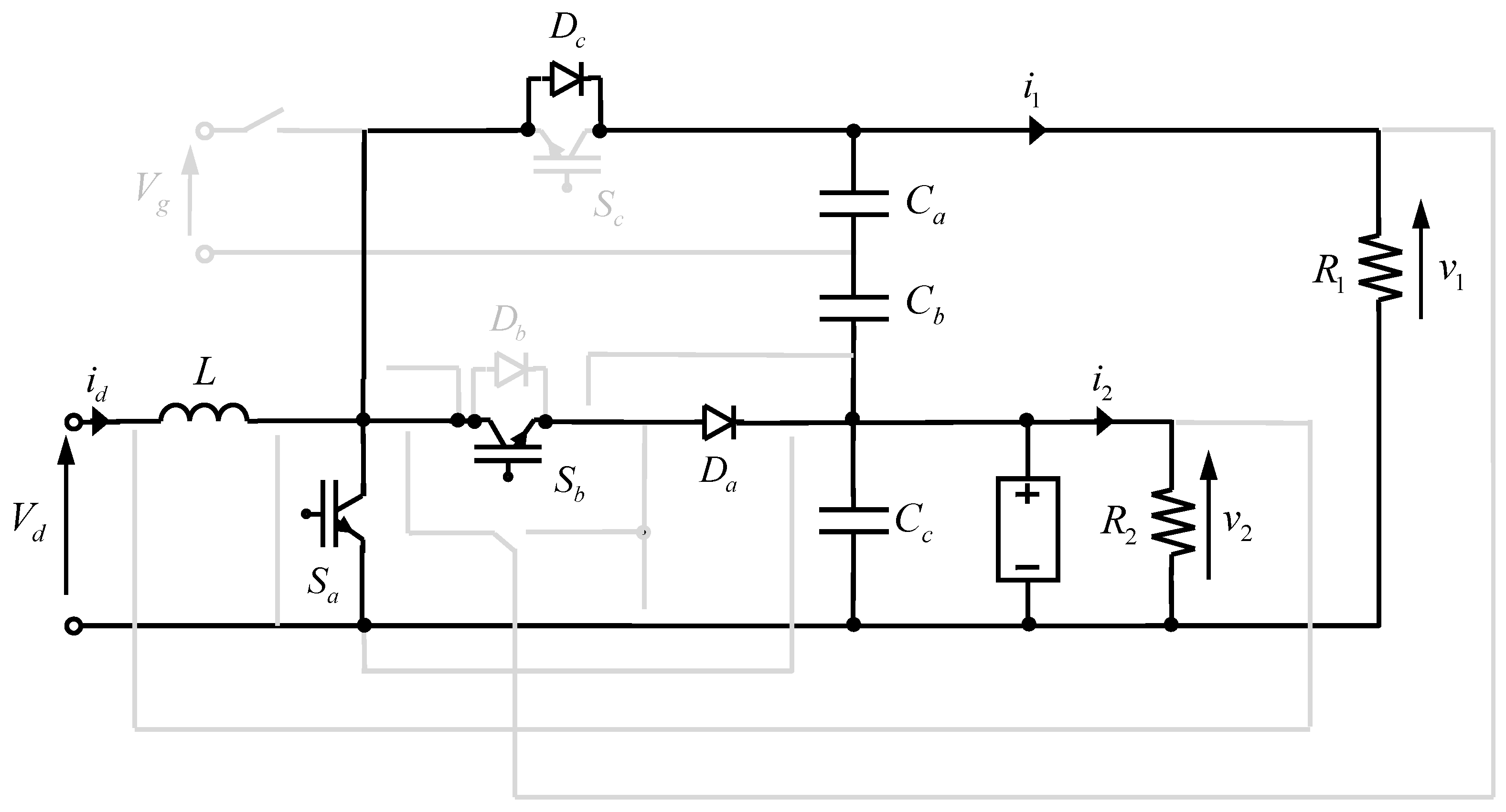
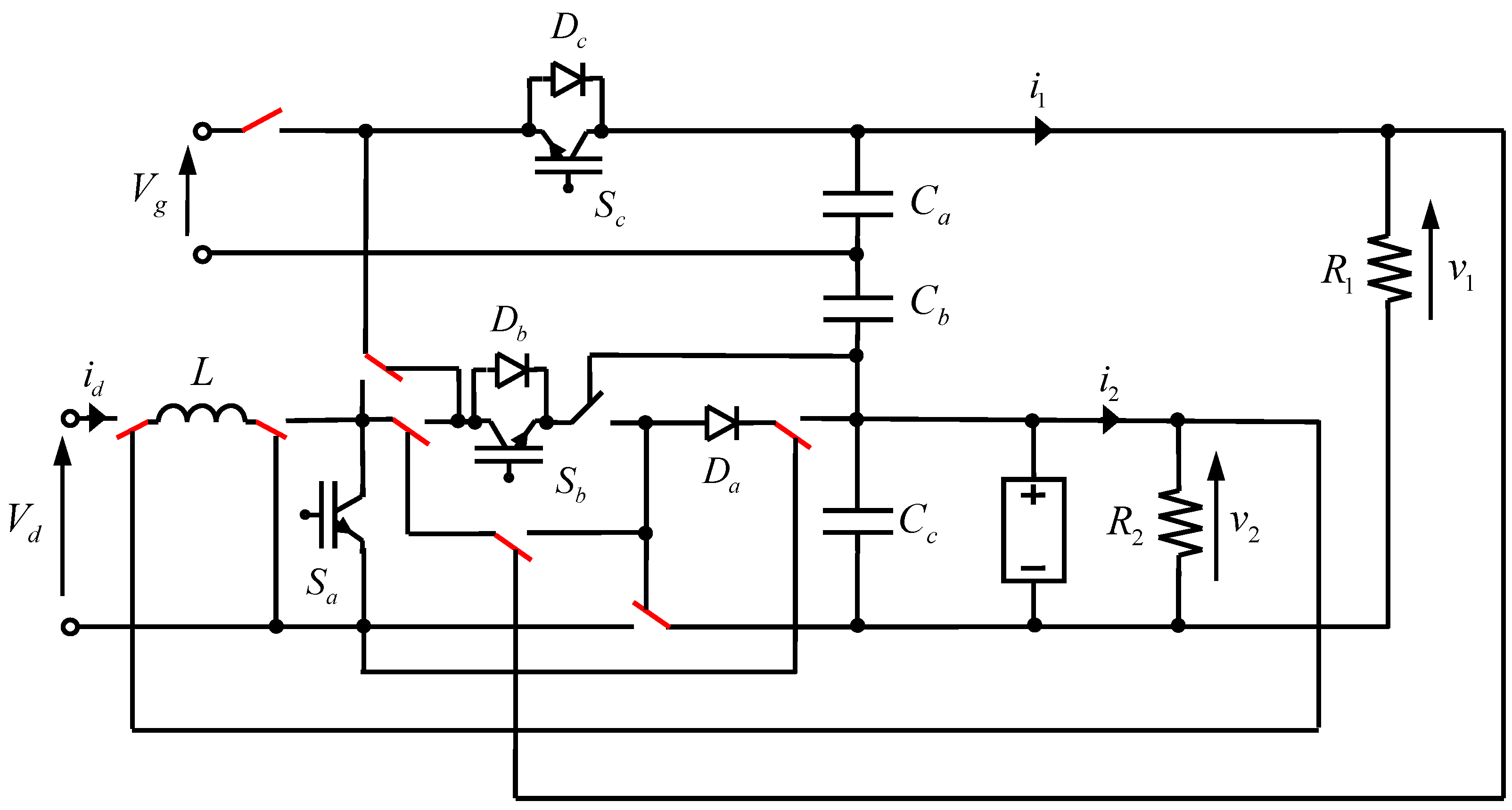
The proposed integrated converter has a reduced number of components,
i.e., switches, diodes, inductors, compared with traditional topologies. This conversion unit is designed to get as much power as possible from renewable generators, provide an alternative feeding source for loads in case of grid brownout and guarantee proper power quality to the load connected. For this purpose the RIC topology includes several static switches, as shown in the basic scheme of
Figure 2.
Figure 2.
Reconfigurable integrated converter.
Figure 2.
Reconfigurable integrated converter.
The two inputs of the RIC are the AC mains, represented by the AC voltage source Vg, and the renewable energy source, represented by the DC voltage source Vd. The two DC loads have voltages v1 and v2, and currents i1 and i2 respectively.
Referring to
Figure 2, the RIC can have different configuration using always the same components. In fact, depending on the status of the static switches, the RIC operates in three different configurations: Double-level Boost Mode; Boost-Rectifier Mode and Buck-Rectifier Mode. The backup battery on the 48 V side enables the function of uninterruptible power supply (UPS). The choice of the specific configuration used is dependent on the availability of the power generated by the renewable source, the battery state of charge (SOC) and the load power. The levels of the two DC voltages can be adjusted to the specific requirements of the grid and the renewable sources used.
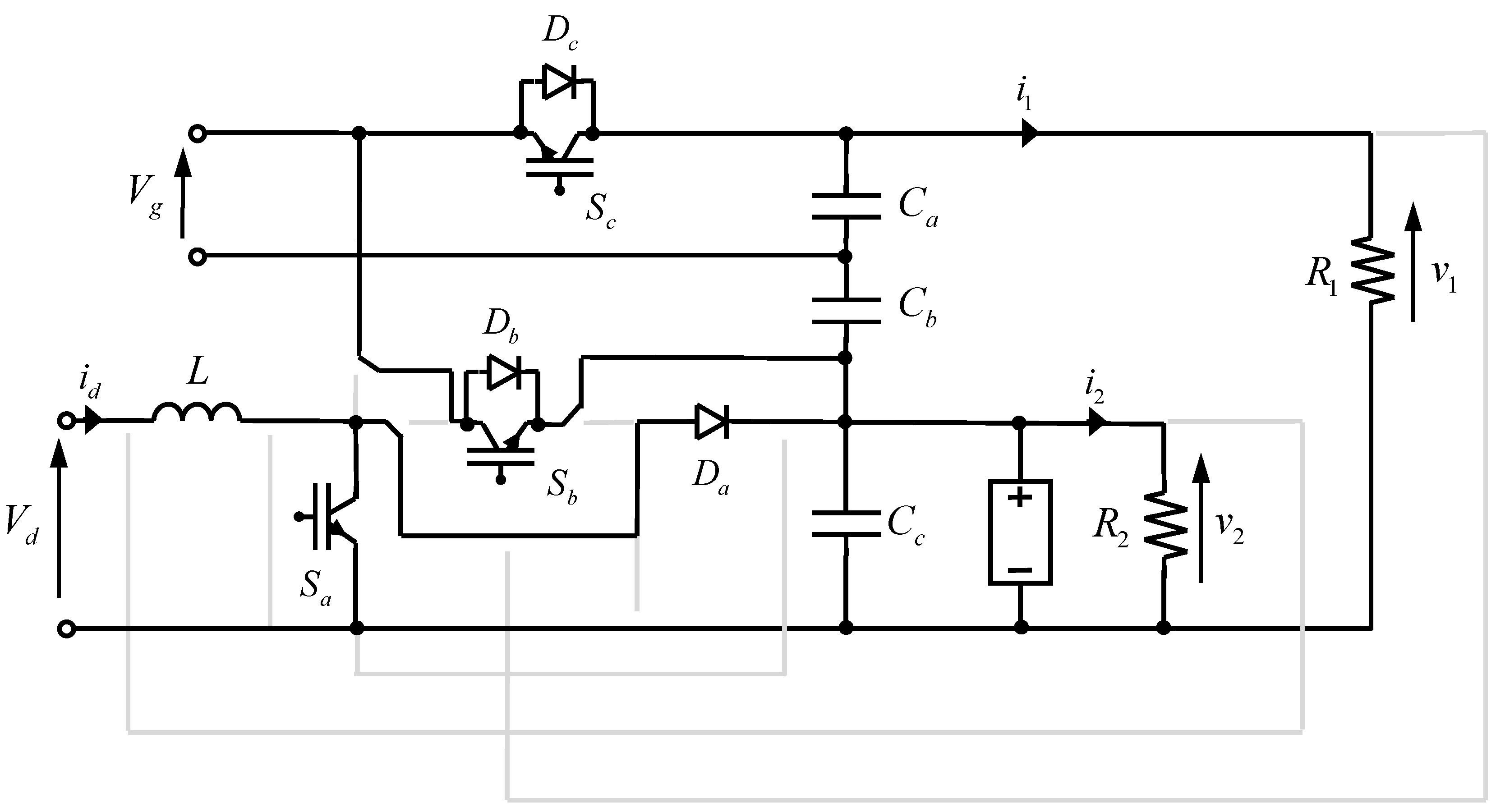
2.1. The Double-level Boost Mode
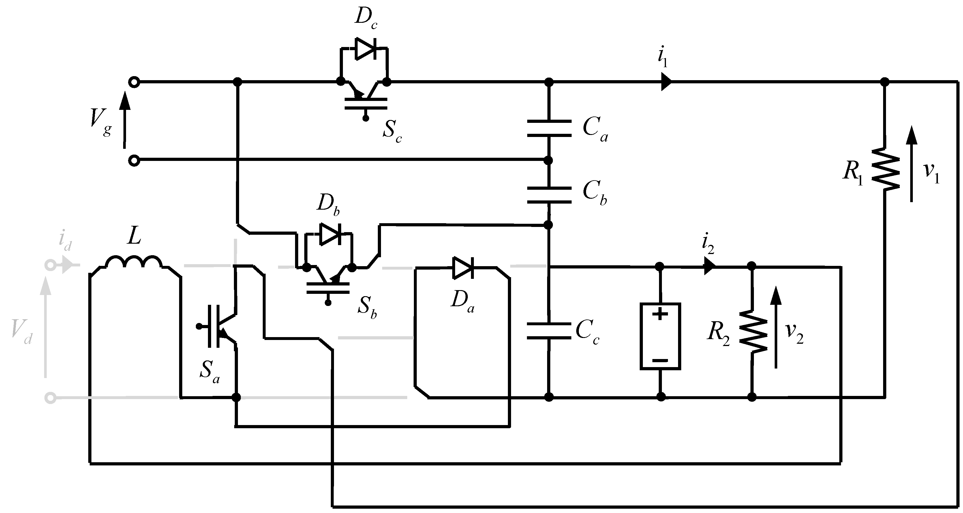
The configuration of the RIC working in Double-level Boost Mode is depicted in
Figure 3. This is the prior mode of operation of the converter and is selected when the RES has the capability of satisfying in full the loads requests. In this case, there is no need to get power from the grid and, since the aim of the RIC is to get as much power as possible from the renewable generator, the surplus power is stored into the battery.
As
Figure 3 shows, the grid is disconnected and all the power comes from the RES. The system operates with only two switches and two diodes, while the switch Sa is not operated and the diode Db is blocked by the diode Da. This configuration is a single inductor dual output topology (SIDO), being only one input inductor designed for all the converter power and two output voltage levels feeding the loads.
Figure 3.
Double-level Boost Mode.
Figure 3.
Double-level Boost Mode.
2.2. The Boost-Rectifier Mode
When RES production is not sufficient to match the load power demand, the AC mains are connected to compensate the unbalance. The grid feeds the larger loads connected to the higher voltage bus. The RIC is then configured to operate as a Boost-Rectifier Mode, with a position of the static switches shown in
Figure 4.
It can be noticed by
Figure 4 that the RES keeps feedings the lower voltage bus. The choice to connect the battery to the lower voltage bus is justified by the intention to get as much power as possible from the RES, eventually storing energy into the battery when no external load is applied. AC power is converted into DC power by means of the upper part of the converter, which is arranged as an active voltage doubler rectifier. Active rectification allows high conversion efficiencies and reduced impact on the AC grid in terms of harmonics generated. It is evident that in this mode the converter includes two independent subsystems: the upper part operates as an active front end, while the lower part operates as a single input single output DC/DC boost converter.
Figure 4.
Boost-Rectifier Mode.
Figure 4.
Boost-Rectifier Mode.
2.3. The Buck-Rectifier Mode
The RIC is also capable of supplying loads independently on RES availability, exploiting the grid as the sole energy source. In this case, the converter operates in Buck-Rectifier mode, whose circuit is represented in
Figure 5.
Figure 5.
Buck-Rectifier Mode.
Figure 5.
Buck-Rectifier Mode.
This mode of operation is selected when the RES is completely unavailable, e.g., during nighttimes, maintenance and/or failures. In the buck-rectifier mode, the converter operates as two cascade systems: a first part includes the component Sa, Da, Sb, Db, Ca, Cb, while the second part is made by the components Sc, Dc, Cc and the inductor L. The upper part is fed by the grid and is an active voltage doubler; the active rectifier feeds the load R1 and the input of the lower part. This section is a buck-boost DC/DC converter feeding the load R2. Thus, the control of the converter has to ensure a duty-cycle lower than 0.5 for the switch Sa.
3. Single Inductor Double Output DC/DC Converter
With reference to the Double-level Boost Mode, the system represented in
Figure 3 can be re-depicted as in
Figure 6 for better clarity. The converter is supplied by a DC voltage source
Vd, supposed perfectly constant.
In that figure, only the components used in this specific operation mode have been reported and the capacitances have been renamed:
Cl matches
Cc of
Figure 2 and
Ch matches the series of
Ca and
Cb. Compared to two traditional boost choppers, the structure is not provided with extra switches or diodes, and a single input inductor is used instead of two. Making reference to the topology depicted by
Figure 6, the possible combinations of the switches are:
- (1)
Sa is on, Sb is off and Dc is off: If Sb is off, Dc is off too because is reverse biased by the series of capacitors Ch and Cl. In this condition, the inductor L is charged by the RES, whereas the capacitors feed the loads R1 and R2. Input and outputs are decoupled in this situation.
- (2)
Sa is off, Sb is off and Dc is on: When Sa is switched off, Dc is directly biased by the voltage across the inductor. In this situation, the energy stored into the inductor is delivered to the loads and the capacitors are charged in series.
- (3)
Sa is off, Sb is on and Dc is off: When Sb is switched on, Dc is reversed biased again by the capacitor Ch. The inductor charges Cl only, whereas Ch feeds the load R1.
Figure 6.
Single inductor double output DC/DC converter.
Figure 6.
Single inductor double output DC/DC converter.
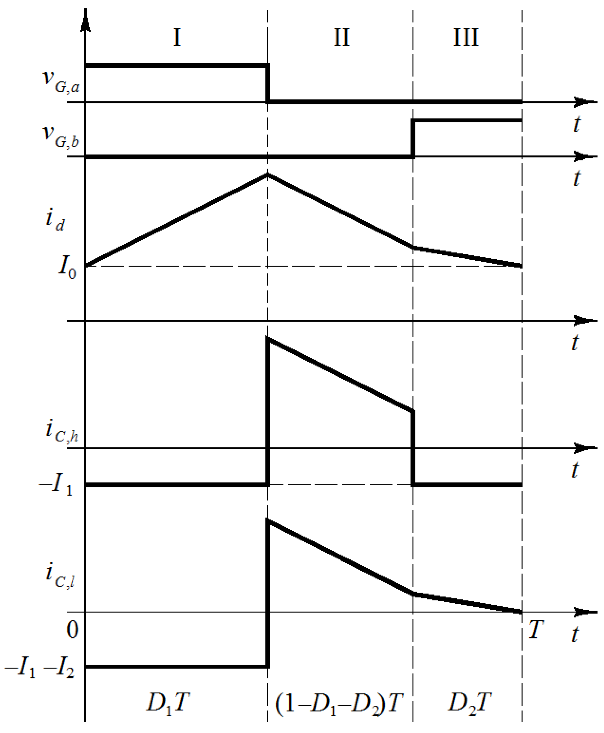
The key waveforms explaining the operating principle of the converter are shown in
Figure 7, where
vG,a and
vG,b are the gate voltages of the switches
Sa and
Sb respectively, and
iC,h and
iC,l are the currents in the capacitors
Ch and
Cl, respectively.
The time intervals when the converter is in the first, second and third state are indicated respectively by D1T, (1 − D1 − D2)T and D2T, where T is the inverse of the switching frequency. Thus, D1 and D2 are the duty-cycles of the switches Sa and Sb respectively, and their value can be easily calculated analysing large-signal steady-state characteristics. The analysis presumes an ideal converter, i.e., no parasitic elements such as the inductor series resistance (Rd) are included. Despite these limitations, the equations presented have adequate accuracy for practical design purposes.
Figure 7.
Key waveforms concerning the operation stages of the proposed converter.
Figure 7.
Key waveforms concerning the operation stages of the proposed converter.
At steady-state conditions, the Volt-second balance of the input inductor gives:
where
V1 and
V2 are the mean values of
v1(
t) and
v2(
t); Equation (1) gives a relation between
D1 and
D2. Moreover, the capacitor charge balance equations give:
where
I0 is the input current at the beginning of each period
T in steady-state conditions. From Equations (1) and (2), in case of large inductances and high switching frequencies, the duty-cycles necessary for obtaining the desired voltages can be easily calculated and their expression are the ones in Equation (3):
where
I1 and
P1 are respectively the average current and power of load 1 and
I2 and
P2 are respectively the average current and power of load 2.
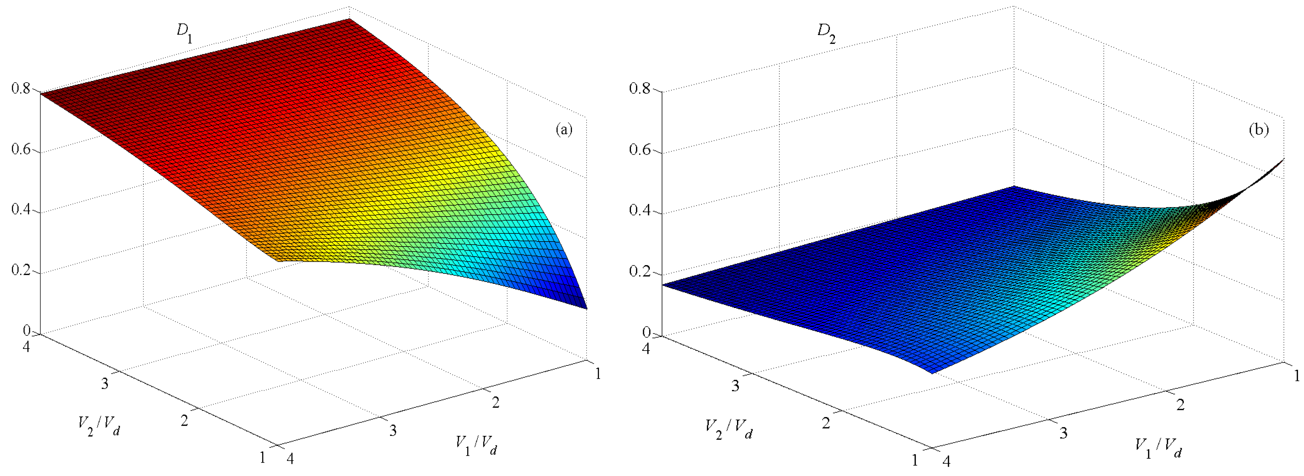
The duty-cycles given by Equation (3) are always both less than one and also their sum is less than one. This is confirmed by the plots of the duty-cycles as a function of the output voltages as shown in
Figure 8.
Figure 8.
Duty cycles of switches as a function of desired output voltage. (a) D1 and (b) D2.
Figure 8.
Duty cycles of switches as a function of desired output voltage. (a) D1 and (b) D2.
The limit of continuous conduction mode is obtained when the input current at steady-state starts from zero at the turn-on of switch
Sa,
i.e.,
I0 = 0. Solving Equation (2) with the additional condition
I0 = 0 and taking into account Equation (1), it is possible to derive analytically the boundary curve between continuous and discontinuous conduction mode in a Cartesian plane having axes
P1 and
P2. Higher inductances and switching frequencies reduce the area of discontinuous conduction mode, whereas the voltage
V2 has opposite effect. In order to avoid discontinuous conduction mode, the power of the load connected at low-voltage bus must be:
When closed-loop controlled, the system keeps the output voltage to the desired value, adjusting the duty-cycles according to the input voltage fluctuations that might occur; these are generally caused by the weather and the sunlight changing.
4. SIDO Converter Numerical Analysis
With reference to the SIDO converter of
Section 2.1, a numerical analysis is carried out in order to investigate about the behaviour of the structure when closed-loop controlled. The simulations are performed using Matlab-Simulink platform and with reference to the nominal value summarized in
Table 1.
The input voltage level can easily be obtained by three photovoltaic panels connected in series. The choice of the higher level for output voltage can be referred to the US electric system, where the grid AC voltage is 110 V rms, while the lower level is intended to supply consumer electronics, LED light bulbs and, perhaps, to recharge electric scooters. The value of inductor and capacitances have been designed using the traditional procedure of setting a maximum ripple for the inductor current and the capacitance voltages, and choosing the first higher value available in the market; in particular, using the numbers of
Table 1, the ripple of inductor current is lower than 2.5%, while the ripple of both capacitance voltage is lower than 0.1%.
The control is inspired by the traditional double-loop scheme used for SISO structures, in which the inner loop sets the current and the outer loop regulates the voltage;
Figure 9 shows the control scheme of the proposed SIDO converter.
Table 1.
Nominal setting value for numerical analysis.
Table 1.
Nominal setting value for numerical analysis.
| Symbol | Description | Value |
|---|
| Vd | Input voltage | 36 V |
| V1 | Higher output voltage | 200 V |
| V2 | Lower output voltage | 48 V |
| fs | Switching frequency | 20 kHz |
| L | Inductance | 1 mH |
| Ch | Top capacitance | 1 mF |
| Cl | Bottom capacitance | 1 mF |
Figure 9.
SIDO converter control scheme.
Figure 9.
SIDO converter control scheme.
In particular in the lower section the control presents a double loop with PI regulator, the outer working on output voltage (
V1) and the inner one working on input current (
id); this produces the reference inductor voltage
VL*. The mean voltage on the inductor is zero, as expressed by Equation (1), but this is true only if the duty-cycles
D1 and
D2 are kept constant, after the transient is completed and the steady-state conditions are reached. Indeed, during the continuous adjustments operated by the closed-loop control the mean value of the inductor voltage in a switching period can be expressed by Equation (5), where the superscript ‘cl’ indicates that the system operates in a closed-loop control condition:
The upper section of control contains another loop with a PI regulator which works on V2 voltage producing the duty cycles D2cl. The duty-cycle D1cl is then calculated by coupling Equation (4) and using the information of VL and D2cl produced by the two control loops.
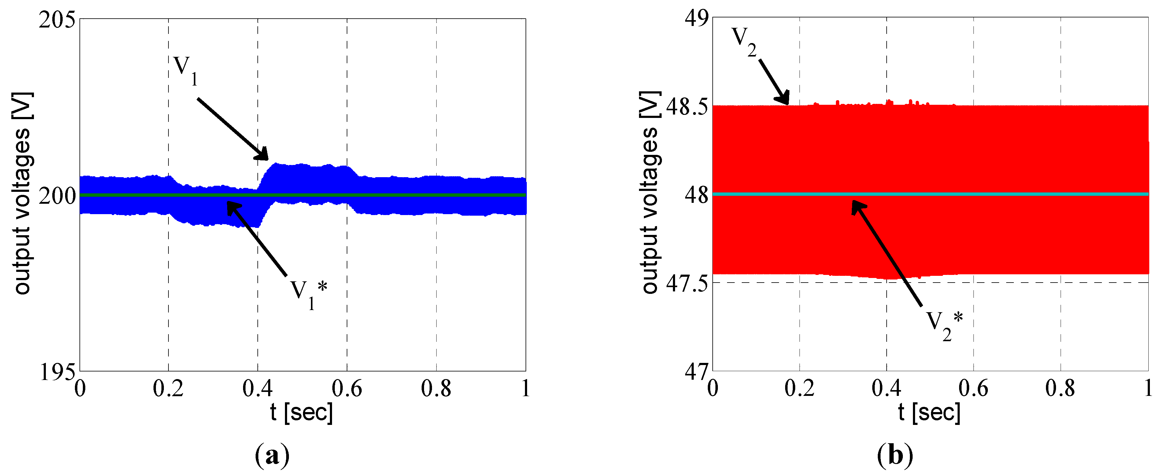
In order to test the converter’s performances and present the waveforms of the main electrical quantities, a first simulation has been made using the nominal values of input and output voltages and electrical loads of 1 kW and 0.5 kW respectively connected to the higher voltage and lower voltage buses. The reference and actual output voltages are shown in
Figure 10. The output voltages follow very well the desired values and this is confirmed by the small ripples visible from the close-up views of
Figure 10. The duty cycles, the inductor current and the instantaneous efficiency of the converter are reported in
Figure 11.
Figure 10.
Fixed voltage and load results: (a) higher output voltage; (b) lower output voltage.
Figure 10.
Fixed voltage and load results: (a) higher output voltage; (b) lower output voltage.
Figure 11.
Fixed voltage and load results: (a) duty cycles; (b) inductor current; (c) converter efficiency.
Figure 11.
Fixed voltage and load results: (a) duty cycles; (b) inductor current; (c) converter efficiency.
At a fixed point, the current and voltage references are accurately tracked and the converter’s efficiency if very high.
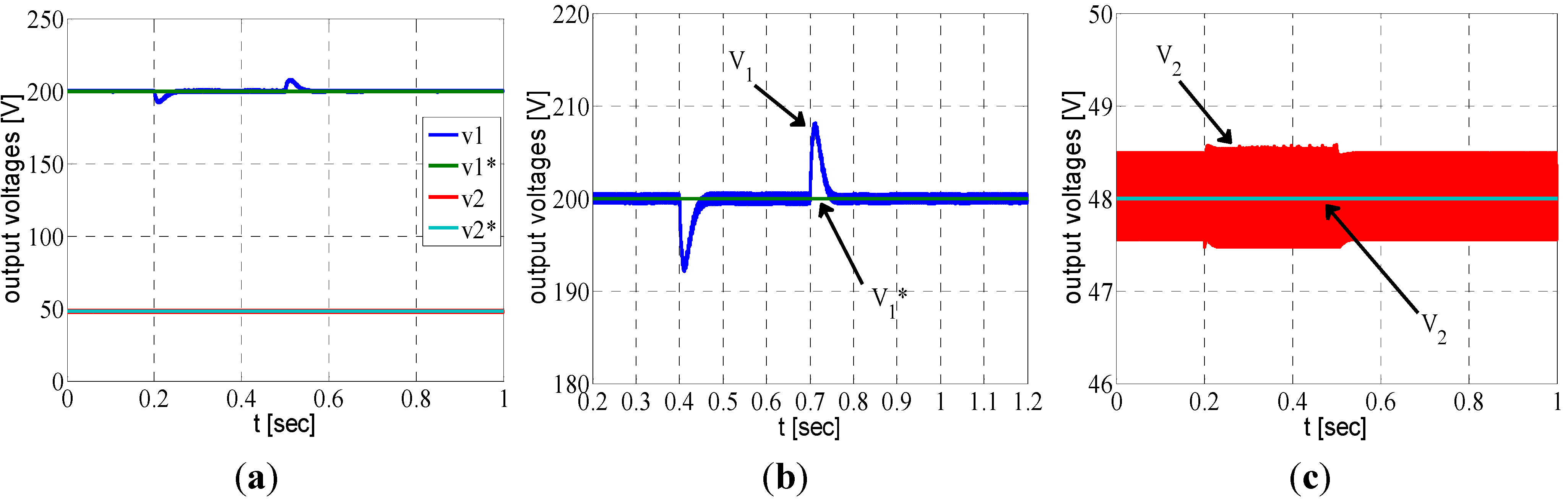
A second set of simulations investigates the response of the system to a variation of the input voltage. In
Figure 12 the RIC is perturbed by a rapid input voltage dip of about 5% of the nominal value, but the effect is barely visible on the output voltages of
Figure 13.
Looking at the close-up view of
Figure 13, it is clear how the variation of input voltage affects the output voltages (mostly the higher level
V1) and the inductor current (
Figure 12a).
Figure 12.
Input voltage variation results: (a) input voltage; (b) inductor current.
Figure 12.
Input voltage variation results: (a) input voltage; (b) inductor current.
Figure 13.
Input voltage variation results: (a) higher output voltage; (b) lower output voltage.
Figure 13.
Input voltage variation results: (a) higher output voltage; (b) lower output voltage.
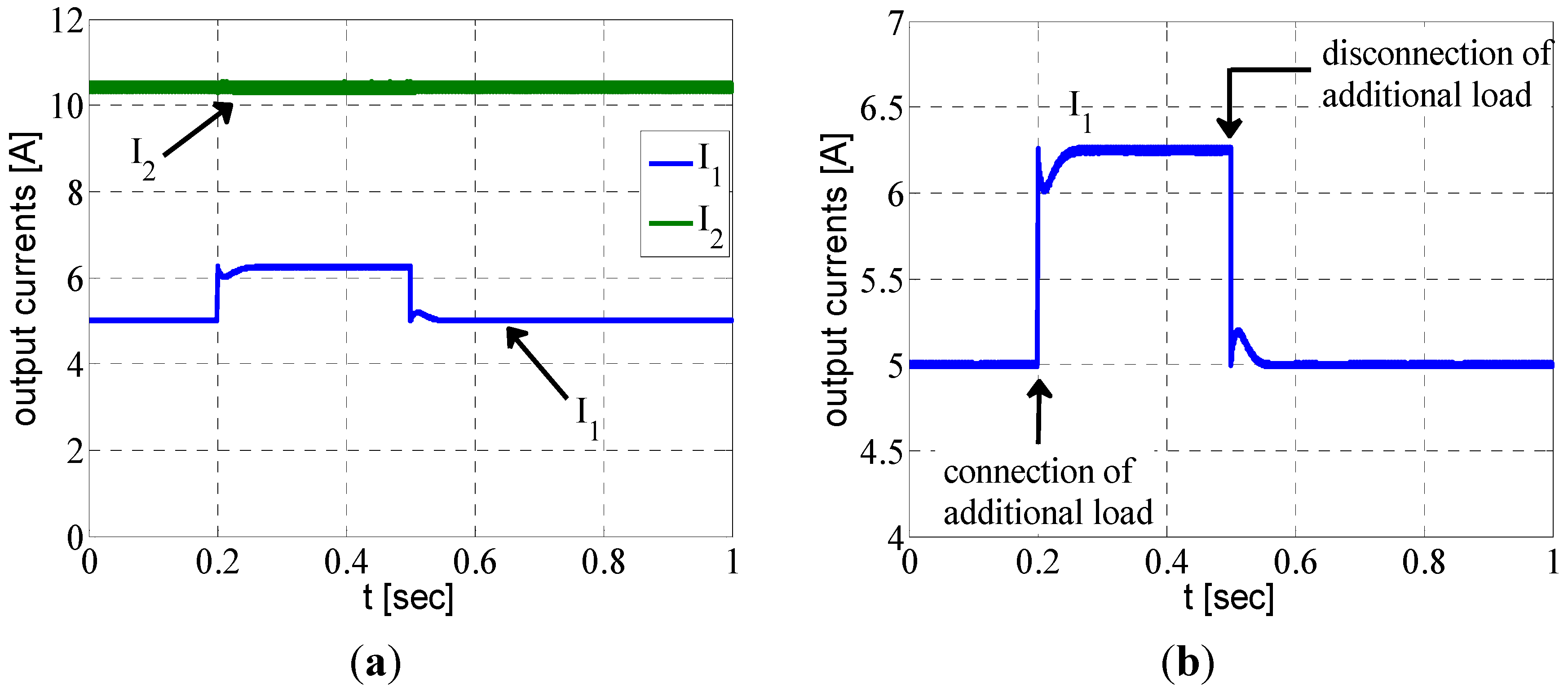
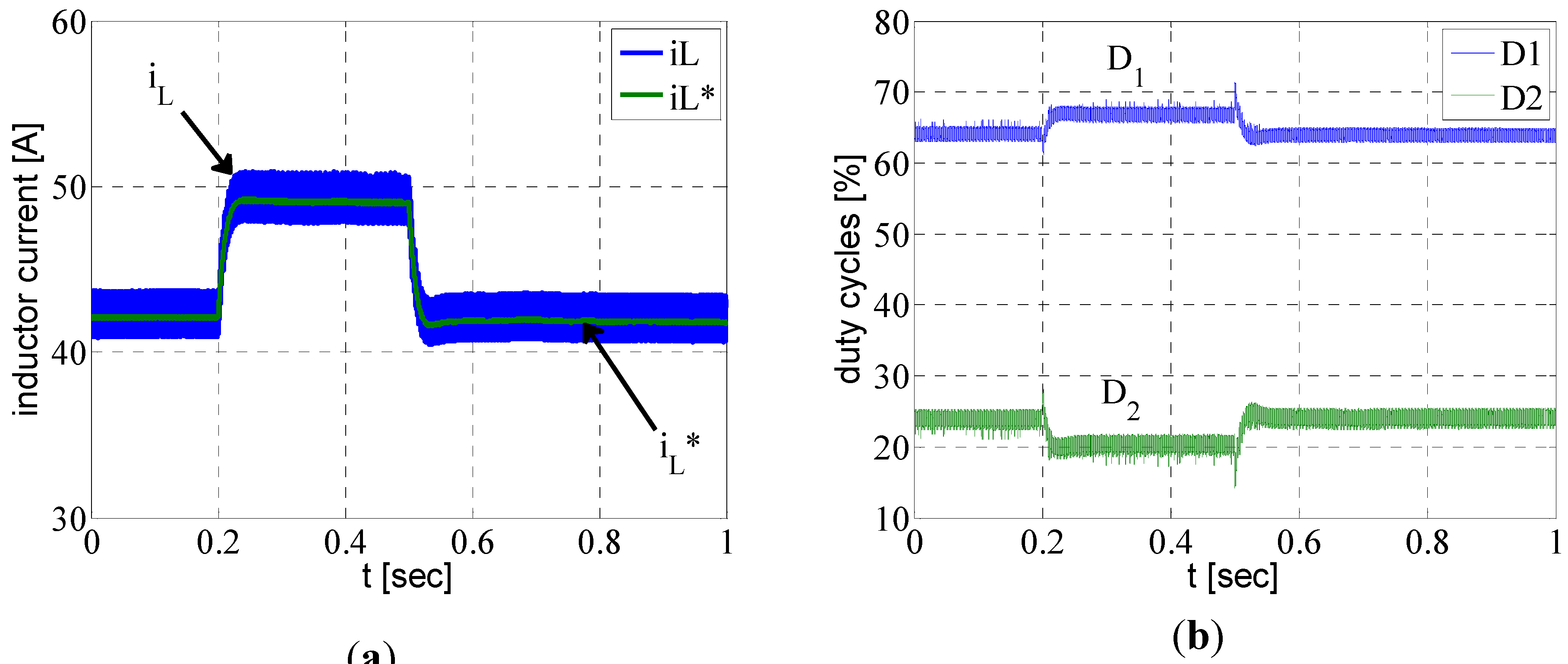
A third simulation analyses a rapid variation of the load. Starting from a load of 1 kW connected to the higher voltage bus and 0.5 kW at the lower voltage bus, at the time
t = 0.4 s, an additional resistive load of 250 W is instantaneously connected to the higher voltage bus, and at the time
t = 0.7 s the additional load is disconnected; during the entire time window, the input voltage of the converter is supposed to be constant. As shown in
Figure 14, the load step variation of 125% produces visible under and over-voltages on the higher output voltage bus, while does not significantly affect the lower voltage bus.
The rapid change in the
I1 output current is clear visible with reference to the right side of
Figure 15 that—in a different scale—can represent the
P1 output power as well; no variation are instead found in the current
I2, as shown in the left side of
Figure 15.
The increase of output power
P1 implies a step variation of the inductor reference current, as evident looking at the left side of
Figure 16.
Figure 14.
Load step variation results: (a) output voltages; (b) higher output voltage; (c) lower output voltage.
Figure 14.
Load step variation results: (a) output voltages; (b) higher output voltage; (c) lower output voltage.
Figure 15.
Double load step variation results: (a) output currents; (b) higher level output current.
Figure 15.
Double load step variation results: (a) output currents; (b) higher level output current.
Figure 16.
Load step variation results: (a) inductor current; (b) duty cycles.
Figure 16.
Load step variation results: (a) inductor current; (b) duty cycles.
The step load variation of 125% at the higher voltage bus produces a variation of the same voltage level, because the rapid change of power requested is initially compensated by the output capacitance. The deviation between reference and measured voltages rapidly modifies the reference of the inductor current, producing a rapid adjustment of the duty cycles (see
Figure 16). As a consequence, the inductor current follows the reference value and the output voltage gets back to the desired value after a deviation that, from the analysis of
Figure 14, is lower than 5%.
Similar results have been observed introducing a 125% load step variation on the lower voltage level; in this case the deviation of output voltages have shown a lower magnitude, since the power P2 is lower than P1.


