Voltage Support Provided by STATCOM in Unbalanced Power Systems

 , and
, and
Abstract
: The presence of an unbalanced voltage at the point of common coupling (PCC) results in the appearance of a negative sequence current component that deteriorates the control performance. Static synchronous compensators (STATCOMs) are well-known to be a power application capable of carrying out the regulation of the PCC voltage in distribution lines that can suffer from grid disturbances. This article proposes a novel PCC voltage controller in synchronous reference frame to compensate an unbalanced PCC voltage by means of a STATCOM, allowing an independent control of both positive and negative voltage sequences. Several works have been proposed in this line but they were not able to compensate an unbalance in the PCC voltage. Furthermore, this controller includes aspects as antiwindup and droop control to improve the control system performance.1. Introduction
The ongoing large-scale integration of wind energy into the power system demands the continuous revision of grid codes and power quality standards in order to fulfill restrictive constraints. Furthermore, most host utilities also require that wind farms must tolerate system disturbances [1]. These requirements become of paramount importance in remote locations where the feeders are long and operated at a medium voltage level, providing a weak grid connection. The main feature of this type of connection is the increased voltage regulation sensitivity to changes in load [2]. Thus, the system's ability to regulate voltage at the point of common coupling (PCC) to the electrical system is a key factor for the successful operation of the wind farm [3], even in the face of voltage flicker caused by wind gusts or post fault electromechanical swings in the power grid [1].
Nowadays, there are grid operators that allow providing unbalanced currents so that the power at the PCC remains constant. This is very useful in weak grids because it allows connecting all loads to a balanced PCC voltage, which is especially important for sensitive loads that could disconnect if the AC voltage does not meet restrictive voltage standards.
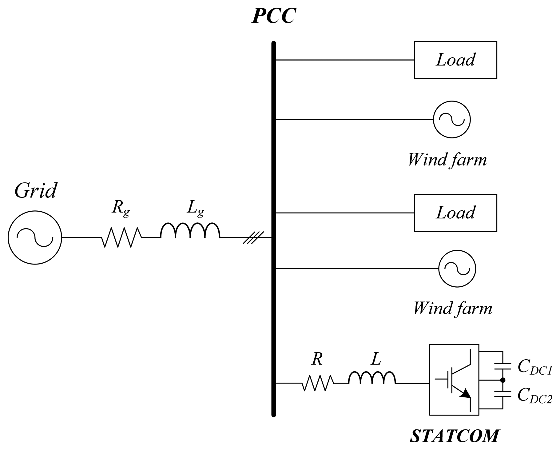
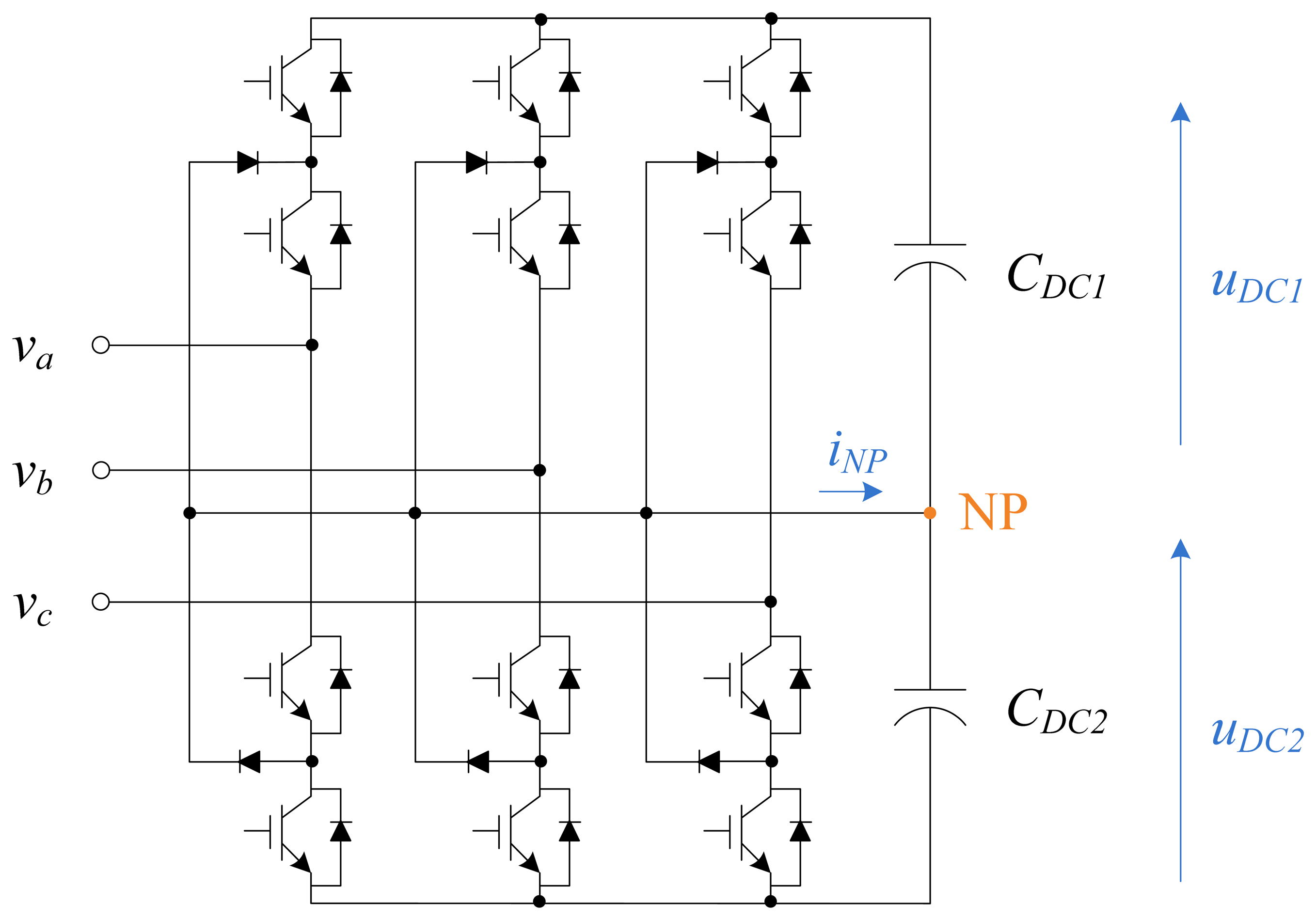
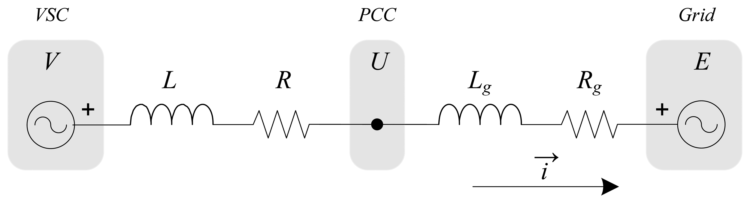
This task can be accomplished by means of a STATCOM, which is a Voltage-Source Converter (VSC) system whose prime function is to exchange reactive power with the host AC system [4] and control the power factor. In a distribution system, it is mainly used for voltage regulation [5]. This has a major application in weak grids, whose significant grid impedance may lead to large PCC voltage variations compared to that of strong grids. The general system under investigation is shown in Figure 1. Several loads and wind farms are connected to the same PCC along with a STATCOM, which is in charge of the PCC voltage regulation. In this figure, L and R are the grid filter parameters, Lg and Rg are the grid impedance parameters, CDC1 and CDC2 are the DC-link capacitors and the STATCOM is a three-level neutral point clamped (NPC) converter.
One of the most typical disturbances in power systems is an unbalance in the PCC voltage [6], which is a difference in the magnitude of the phase-to-neutral (or phase-to-phase) voltages of a three-phase system. There is no standardized mathematical expression to quantify the unbalance of a three-phase system. Three definitions of unbalance are reviewed in [7]; one was developed by the National Equipment Manufacturer's Association (NEMA), another was developed by the IEEE and the other is the most common definition used by engineering community (the so-called true definition). The latter expresses the voltage unbalance factor (VUF) in percent as:
It is well-known that any three-phase system can be split into the sum of three balanced systems, namely, positive, negative and zero sequences. A balanced three-phase system will be only composed of a positive sequence system. However, in real power systems several types of disturbances may affect the grid and give rise to the appearance of a negative sequence system in addition to the positive sequence one. Zero sequence systems only appear in three-phase four-wire power systems [8] and this case is not tackled in this article, since a three-phase three-wire power system is considered.
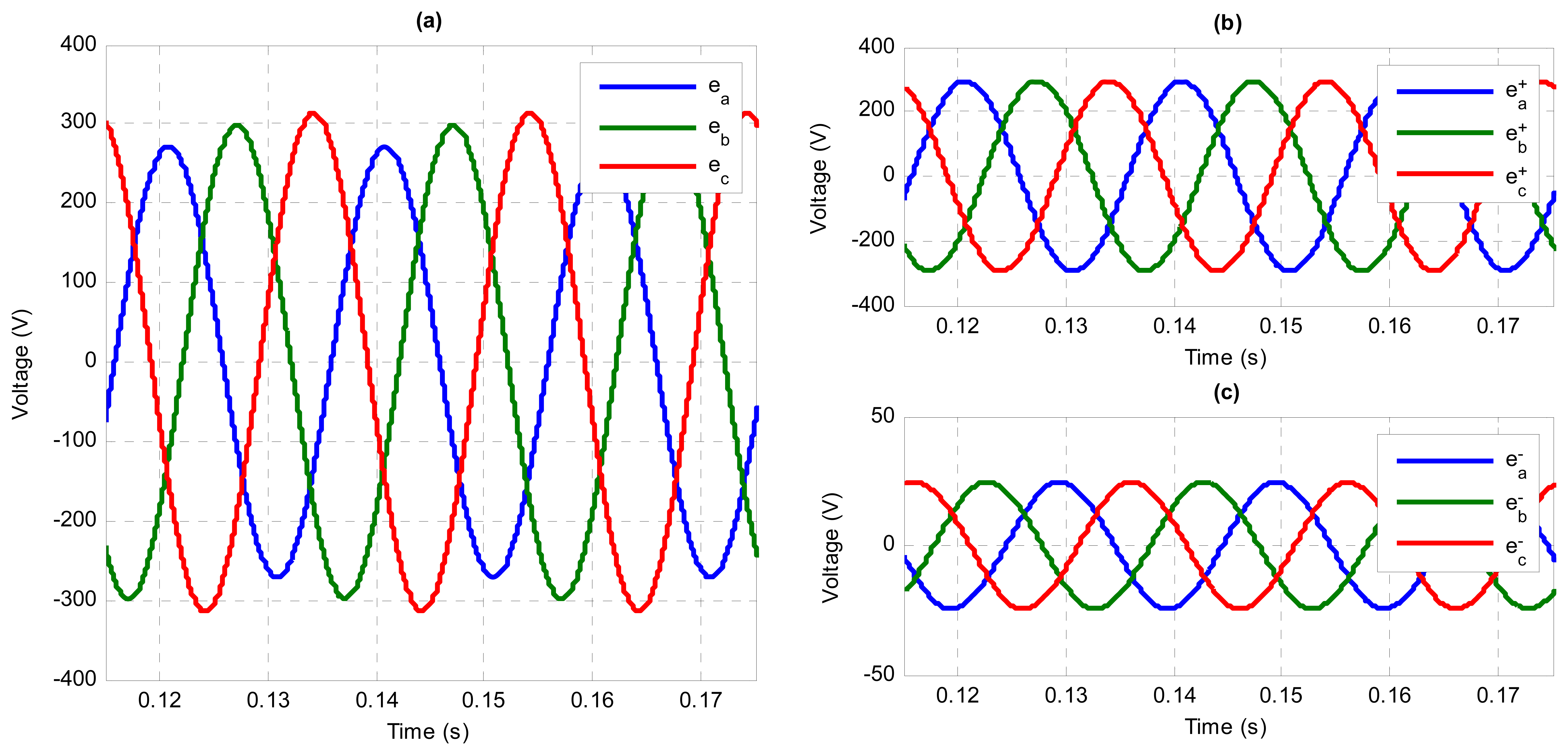
The unbalanced three-phase voltage shown in Figure 2a has a VUF equal to 8.3%, and it has been considered as the ideal grid voltage in the simulations results of Section 6.1. It is composed of the sum of a positive sequence three-phase system with (Figure 2b) and a negative sequence three-phase system with (Figure 2c). In accordance with IEC 61000-3-13, the maximum VUF during normal operation in transmission systems must not exceed 2%; therefore, the grid voltage of Figure 2a can be used to justify and test the proposed algorithm.
An unbalanced voltage has several negative effects. For instance, it reduces efficiency and can cause failure in induction machines [9]. It also produces negative effects on power electronic converters. The voltage unbalance can impair a Pulse-Width Modulation (PWM) converter system because the input active and reactive power ripples are generated by the cross products of line currents and unbalanced voltages [10]. The grid synchronization algorithm has to be sufficiently fast and accurate to extract the positive and negative voltage sequences precisely, in order to generate the output current references. A PCC voltage controller is needed to cancel these harmful effects while allowing an independent control of positive and negative sequence components.
The article is organized as follows: Section 2 analyzes the PCC voltage equations under unbalanced conditions and provides their corresponding plant models, which are focused in the grid model under a voltage unbalance. Section 3 details the control scheme that has been developed, as well as the design and tuning of the proposed PCC voltage controller. Section 4 addresses the possibility of performing an online adaptation of the DC-link reference voltage to always ensure an optimal modulation index. Section 5 investigates the sampling mode of the PCC voltage when working with an L-filter, which is of paramount importance for the correct operation of the control system in weak grids. Section 6 shows the effectiveness of the novel PCC voltage control through simulation results and, lastly, conclusions are presented in Section 7.
2. Grid Modeling Under Unbalanced Conditions
A VSC can be represented as an ideal AC voltage source (per phase). Therefore, its connection to the grid can be depicted according to the scheme of Figure 3, where L and R are the grid filter parameters, Lg and Rg are the grid impedance parameters, V is the VSC output voltage, U is the PCC voltage, E is the ideal grid voltage and ι⃗ is the current flowing from the VSC to the grid.
In order to obtain a general model of the grid, valid for both balanced and unbalanced conditions, the scheme of Figure 3 is considered. The grid model is calculated from the voltage equation between the points U (PCC) and E (ideal grid). The grid filter is not taken into account to obtain such model, since PCC voltage variations in an unbalanced system are imposed by the grid impedance and not by the grid filter.
The grid model can be expressed in time domain and in synchronous reference frame (dq-axes) as shown in Equation (2a) for positive sequence (superscript “+”) and Equation (2b) for negative sequence (superscript “−”). In these equations, ω1 is the fundamental angular frequency ω1 = 2π50 rad/s. Each PCC voltage component is formed by the voltage drop across the grid impedance, a cross-coupling term between axes and the ideal grid voltage:
Each of these voltages is separated into its d and q projections: positive sequence voltages and are shown in Equation (3a) and (3b), whereas negative sequence voltages and are shown in Equation (4a) and (4b). These four expressions are steady-state approximations. Grid resistance Rg is considered to be very small, so that its contribution to the PCC voltage can be neglected (compared to the voltage drop across the grid filter inductance). Furthermore, the derivative of a constant signal (such as ι⃗ in dq-axes) is zero. Note that is equal to zero Equation (3a) because a Phase-Locked Loop (PLL) is used to synchronize the positive sequence PCC voltage vector (u⃗+) with the q-axis, hence the projection of u⃗+ on this axis is equal to its amplitude :
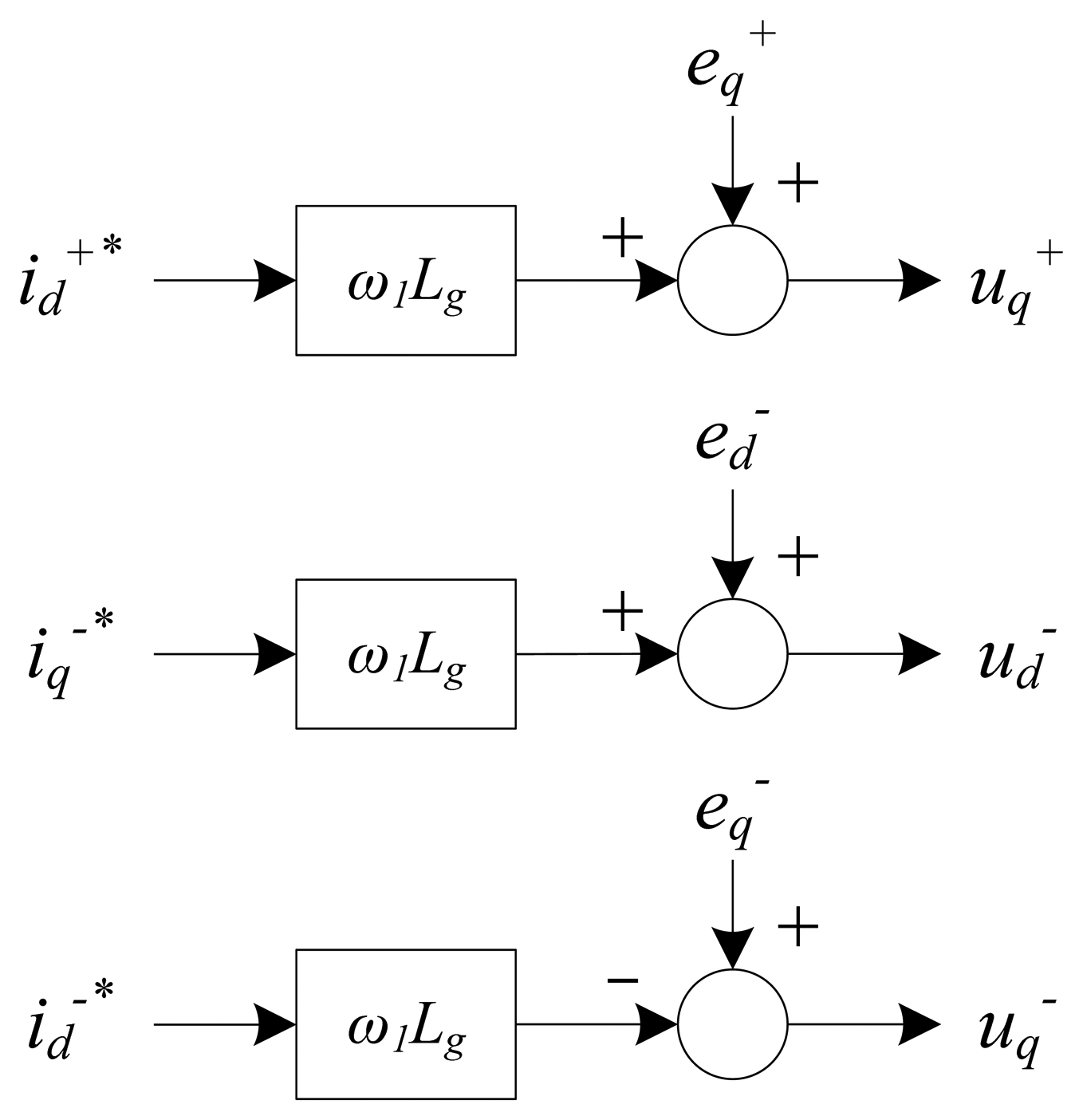
From the above equations it is straightforward to observe that each PCC voltage component is related to only one current component: and ; and ; and and . The current component is related to the control of the DC-link voltage and does not influence the PCC voltage level directly. Thus, three independent voltage controllers are needed for , and . Since they are constant voltages, a Proportional-Integral (PI) controller is enough to ensure zero steady-state error. The plant models needed for the design of these controllers are shown in Figure 4 for each component, based on Equation (3b) and (4).
3. Control Scheme
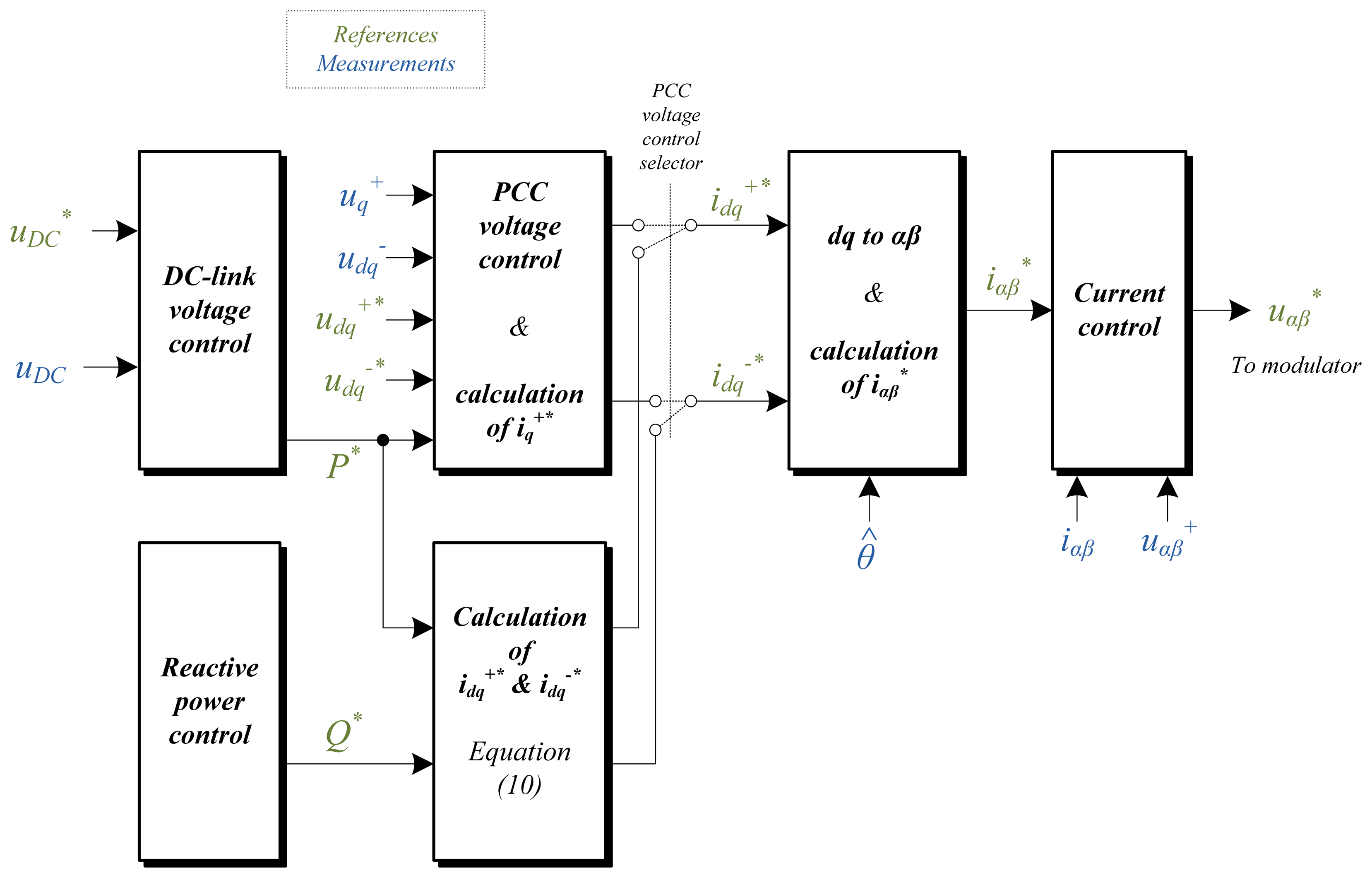
The block diagram of the proposed control scheme is shown in Figure 5, which is composed of the following parts:
DC-link voltage control
Reactive power control
PCC voltage control & calculation of
Calculation of and
Current control
Modulation strategy
In first place, the active power reference P* is set by the “DC-link voltage control” block. Its output constitutes an input for two possible blocks, namely, “Calculation of and ” block or “PCC voltage control & calculation of ” block. Depending on the application, one block or another will be chosen. The output of both blocks is the dq-axes reference current (positive and negative sequence, and ). The following stage is the dq to αβ transformation plus the calculation of . Finally, the low level control is performed by the “Current control” block and the modulation strategy.
3.1. DC-link Voltage Control
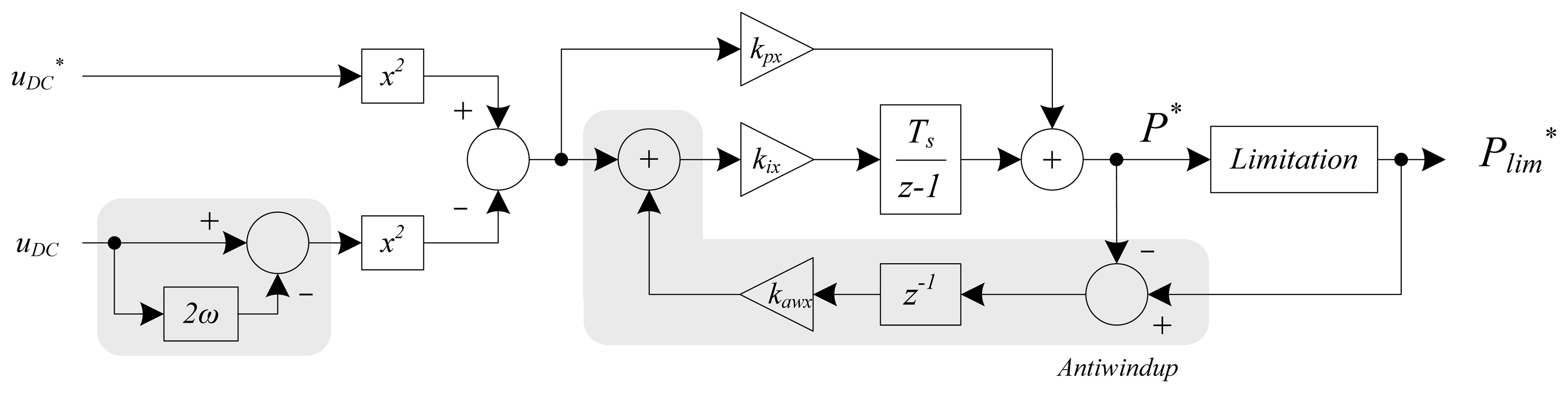
The DC-link voltage controller is usually based on a PI controller along with an antiwindup mechanism. However, this scheme may not be sufficient in the case of weak grids. Due to the compensation of the negative sequence voltage at the PCC, an oscillation of frequency 2ω1 appears in uDC. If uDC is not filtered, this oscillation propagates through the control system, appearing in P* and, therefore, in the reference currents. The oscillation of frequency 2ω1 in dq-axes is transformed into an oscillation of frequency 3ω1 in the abc-axes.
In short, if uDC is not filtered, the PCC currents will be affected by the appearance of a 3rd order harmonic (this being no zero-sequence harmonic). To eliminate this harmonic, the 2nd order oscillation is removed from the measured uDC by means of a band-pass filter centered at ω0 = 2ω1. This filter is implemented with a Second Order Generalized Integrator for Quadrature Signal Generation (SOGI-QSG) [11], using the output in phase with the input since its transfer function behaves as a band-pass filter centered at ω0. This way, the dynamics of the mean value of the DC-link voltage is not altered.
The block diagram of the DC-link voltage controller is shown in Figure 6, where kpx is the proportional gain, kix is the integral gain and kawx is the antiwindup gain. The DC-link model based on the energy stored in the capacitor has been used [12]. As mentioned before, the basis of the DC-link voltage control is a PI controller and its parameters are tuned without taking into account the inner current controller. To do so, the Zero-Order Hold (ZOH) method has been applied to the plant to obtain its discrete time version, where CDC = (CDC1·CDC2)/(CDC1+CDC2):
The PI controller can be expressed in pole-zero form as:
3.2. Reactive Power Control
This is a controller associated to variables that modify the reactive power at the PCC. In this case, this block specifies the reactive power reference Q*, which is an output to the block “Calculation of & ”. Another variable that could be used to modify the reactive power at the PCC is the power factor.
3.3. Calculation of and
This controller is regulated by the equation system in Equation (10). It relates active power, reactive power, PCC voltage and current in dq-axes and it is usually employed in active and reactive power control, as well as in power factor control. Active and reactive powers are divided into three parts: average power (P and Q), oscillating power with cosine terms [P2ω(c) and Q2ω(c)] and oscillating power with sine terms [P2ω(s) and Q2ω(s)]. If grid conditions are balanced, these four oscillating powers are zero and there are only positive sequence voltages and currents. Multiplying by the inverse matrix, the corresponding expressions for the calculation of the reference currents are obtained ( and ). To do so, P2ω(c) and P2ω(s) are set to zero to compensate the unbalance caused by negative sequence voltage and Q2ω(c) and Q2ω(s) are not controlled, therefore their corresponding rows are eliminated from Equation (10). Trying to control these oscillating reactive powers only deteriorates the control performance, therefore they are allowed to run freely:
3.4. PCC Voltage Control
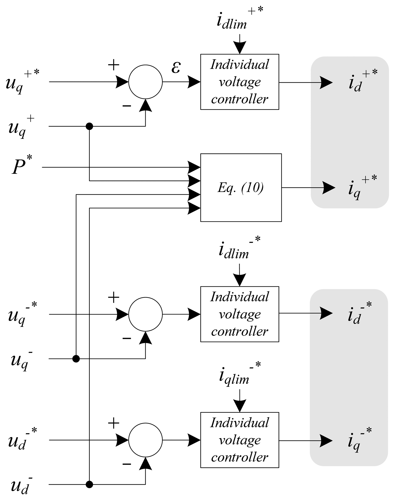
The block diagram of the PCC voltage controller is shown in Figure 7 and it is implemented in dq-axes. This stage is formed by three “individual voltage controllers” in parallel, whose outputs are , , and , plus the calculation of by means of Equation (11). This equation is obtained from Equation (10). The minus sign that goes with is due to the current direction. These four outputs are the references for the current controller. In this figure, ε represents the error signal and the subscript “lim” stands for “limited”. The reference voltages and are set to zero in order to eliminate the PCC voltage negative sequence, whereas the reference voltage should be equal to the PCC fundamental voltage.
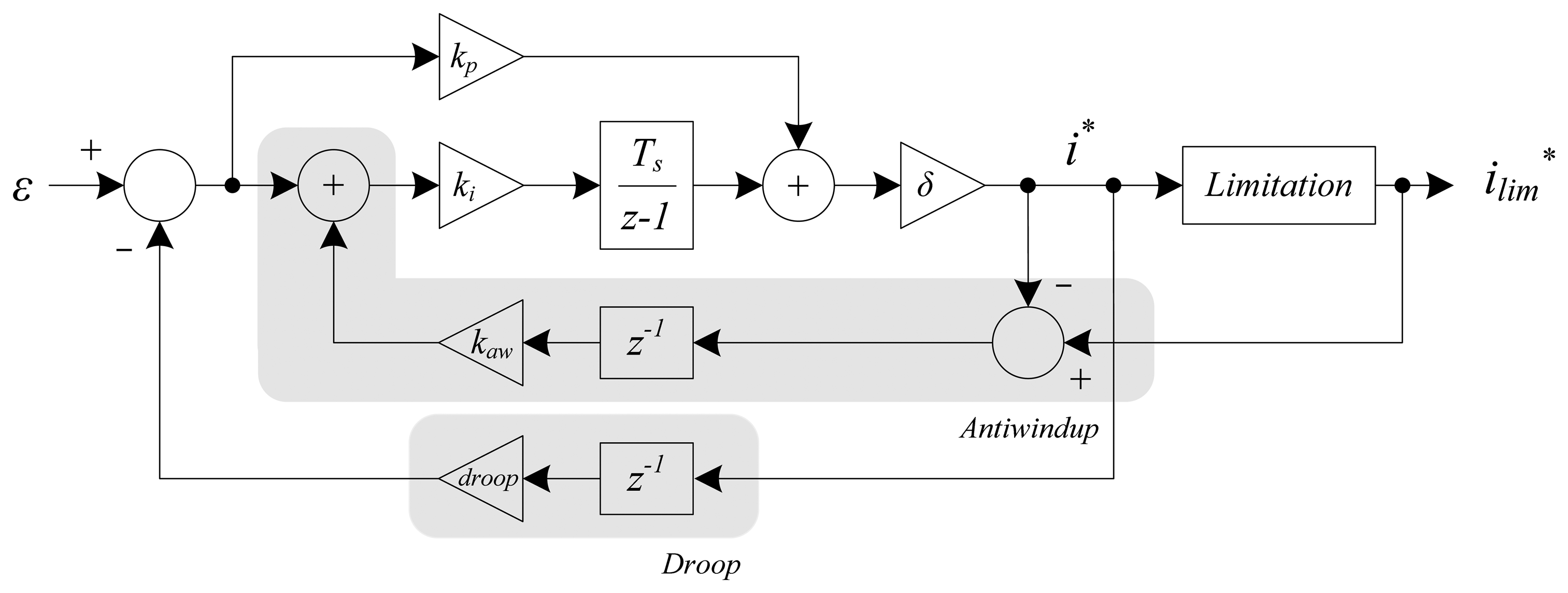
The inner structure of each “individual voltage controller” is depicted in Figure 8. As mentioned, it is mainly formed by a PI controller with a forward Euler integrator. The constant δ is 1 for the voltage controllers of and , and -1 for the voltage controller of due to the minus sign in Equation (4b). It is a first order system and, considering the cascaded system of Figure 5, the tuning goal is to achieve a settling time larger than ten times the settling time of the current controller (ts|vc > 10 · ts|cc, where ts is the settling time, “vc” means voltage control and “cc” means current control). This constraint affects the position of the closed-loop pole introduced by the PI controller. The integral constant (ki) helps achieve zero steady-state error in the event of model mismatch and disturbances. Therefore, the parameter tuning is focused on settling time and controller bandwidth. The resulting parameters are kp = 0.05 and ki = 350.
In order to prevent the windup of the integrator, an antiwindup mechanism has been added to each PI controller. It is characterized by the antiwindup constant, which has been set as kaw = 0.1. High values for this parameter cause system instability. When using an antiwindup technique, an important detail to be taken into account is that its contribution should not be added to the integral branch of the PI controller until the whole control system starts. Otherwise, the control system would be forced to start with a non-zero error.
The linear operating range of a STATCOM with given maximum capacitive and inductive ratings can be extended if a regulation “droop” is allowed. Regulation “droop” means that the terminal voltage is allowed to be smaller than the nominal no-load value at full capacitive compensation and, conversely, it is allowed to be higher than the nominal value at full inductive compensation [13]. It also ensures automatic load sharing with other voltage compensators. Perfect regulation (zero droop or slope) could result in poorly defined operating point, and a tendency of oscillation, if the system impedance exhibited a “flat” region (low impedance) in the operating frequency range of interest [13]. It should be mentioned that this possible regulation makes sense in scenarios where there are several converters connected in parallel trying to control the PCC voltage. This droop control has been added to the voltage controller as shown in Figure 8, characterized by the constant droop = 0.01. Similarly to kaw, high values for this parameter cause system instability. The expression in Equation (11) is obtained from Equation (10).
3.5. dq to αβ Transformation and Calculation of
The outputs of the first stage of the control scheme are and . These current references have to be transformed to αβ-axes, since the current controller is implemented in stationary reference frame. The reason for this is that a resonant controller tuned at ω in αβ-axes is able to compensate both positive and negative sequences, whereas in dq-axes two controllers would be necessary, a PI controller and a resonant controller tuned at 2ω1. The fact of increasing the number of controllers connected in parallel endangers the system stability and increases the settling time of the controller.
Positive and negative sequence current references in αβ-axes are calculated as shown in Equation (12a) and (12b). The estimated phase angle θ̂) of the positive sequence voltage vector is obtained with a PLL, whose bandwidth is 20 Hz. This results in a good tradeoff between selectivity, steady-state error and response speed. Afterwards, the final current references are calculated according to Equation (13a) and (13b):
3.6. Current Controller
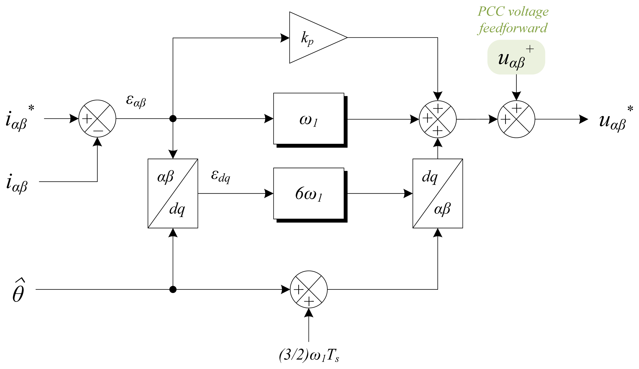
The third stage of the control scheme is the current controller. The harmonics present in power systems are those of order 6k ± 1 (k ∈ ℤ), which turn into 6k (k ∈ ℤ) when changing the reference frame from stationary (abc or αβ) to synchronous (dq). This allows halving the number of resonant controllers needed to implement the current controller [14]. Therefore, since the 5th (negative sequence) and 7th (positive sequence) harmonics are usually present in the grid, the current control scheme of Figure 9 has been used to obtain the simulation results. It consists of two resonant controllers (SOGIs) tuned at ω1 and 6ω1 (the blocks labeled as “ω1” and “6ω1” are composed of an integral gain ki connected in series with a SOGI), a feedforward of the positive sequence PCC voltage, and αβ to dq and dq to αβ transformations. A feedforward of the total PCC voltage (including negative sequence) would introduce non-desired harmonics in the control. The error signals in αβ-axes and dq-axes are εαβ and εdq, respectively.
In general, the resonant frequency of the SOGI is represented by ω0. The discrete SOGI transfer function is given by Equation (14) and, if , which is verified for Ts < 1.4 ms (supposing that is small enough, i.e., a factor of 10) and if ω0 = 2π50 rad/s, Equation (14) can be approximated by Equation (15):
The SOGI is combined with a proportional and integral gain (kp and ki, respectively) to form the current controller. The resulting transfer function can be expressed as:
To help decreasing the computational burden, the trigonometric functions employed in the calculation of these transformations can be implemented by means of look-up tables if the digital platform has enough memory.
3.7. Modulation Strategy
The NPC converter, whose scheme is shown in Figure 10, has some drawbacks such as the additional clamping diodes, a more complicated PWM switching pattern design and possible deviation of neutral point (NP) voltage [15]. The capacitors can be charged or discharged by neutral current iNP, causing NP voltage deviation. It might appear a ripple of frequency three times the fundamental in uDC1 and uDC2 that can destroy components if both DC-link voltages are not balanced.
To minimize this effect, a carrier-based PWM strategy with zero-sequence voltage injection [16] is applied to the three-level NPC converter. Using this technique, the locally averaged NP current is kept to zero, and consequently, the locally averaged voltages on the DC-link capacitors are constant [17].
4. Online Adaptation of the DC-Link Reference Voltage
To enable the power transfer between the grid and the DC-link capacitors, uDC must be greater than vLL, where vLL is the RMS phase-to-phase NPC output voltage. When calculating the reference DC-link voltage, a safety margin ΔuDC is usually given to ensure the energy transfer in case of voltage fluctuations. This margin takes values from 20 V to 50 V in weak grids. Therefore, the calculation of is shown in Equation (18):
When the PCC voltage is expected to suffer large variations, as in the case of weak grids, should be recalculated online to adapt its value to the actual AC voltage. In this way, the modulation index is kept around its optimal value, i.e., ma ≈ 1. Otherwise, the modulation index will be altered, which can increase the converter power losses, modify the expected harmonic content and worsen the overall system performance [15]. It is also advisable to limit the possible values of so that controllability is always ensured, as in the case of voltage dips, and limit the transition rate of
5. Sampling Mode When Working With an L-Filter
One of the essential parts of the converter control is the synchronization system, which allows detecting the angle of the PCC voltage vector. This angle would coincide with that of the grid voltage if it were an ideal grid. Generally, the grid impedance is neglected in terms of controller design, considering the voltage at the PCC as the system voltage [18].
Blasko et al. [19] established that the optimal moment to sample the currents are those in which the PWM carrier signal reaches its maximum and minimum value, since it is in those moments when the zero-crossing of the current ripple takes place. When working with an LCL-filter and a non-ideal grid, and sampling the PCC voltage at those same moments, the obtained PCC voltage in dq-axes corresponds to its actual value. However, this is not the same situation when working with an L-filter and a non-ideal grid. In this case, the PCC voltage presents a ripple in which two envelopes can be seen. By sampling synchronously with the sampling period of the currents, which is also the controller sampling period, the obtained PCC voltage corresponds to one of those envelopes, giving rise to incorrect projections of the PCC voltage on the dq-axes.
Briz et al. [20] posed two alternative methods to the method suggested by Blasko for sampling the currents, when the inverter is connected to a load whose natural frequency may be close to the sampling frequency. In such cases, the method based on the maximum and minimum points of the carrier signal introduces an error at the current fundamental frequency as well as aliasing problems. The methods the authors proposed were based on advancing the sampling instant and on multi-sampling per switching period.
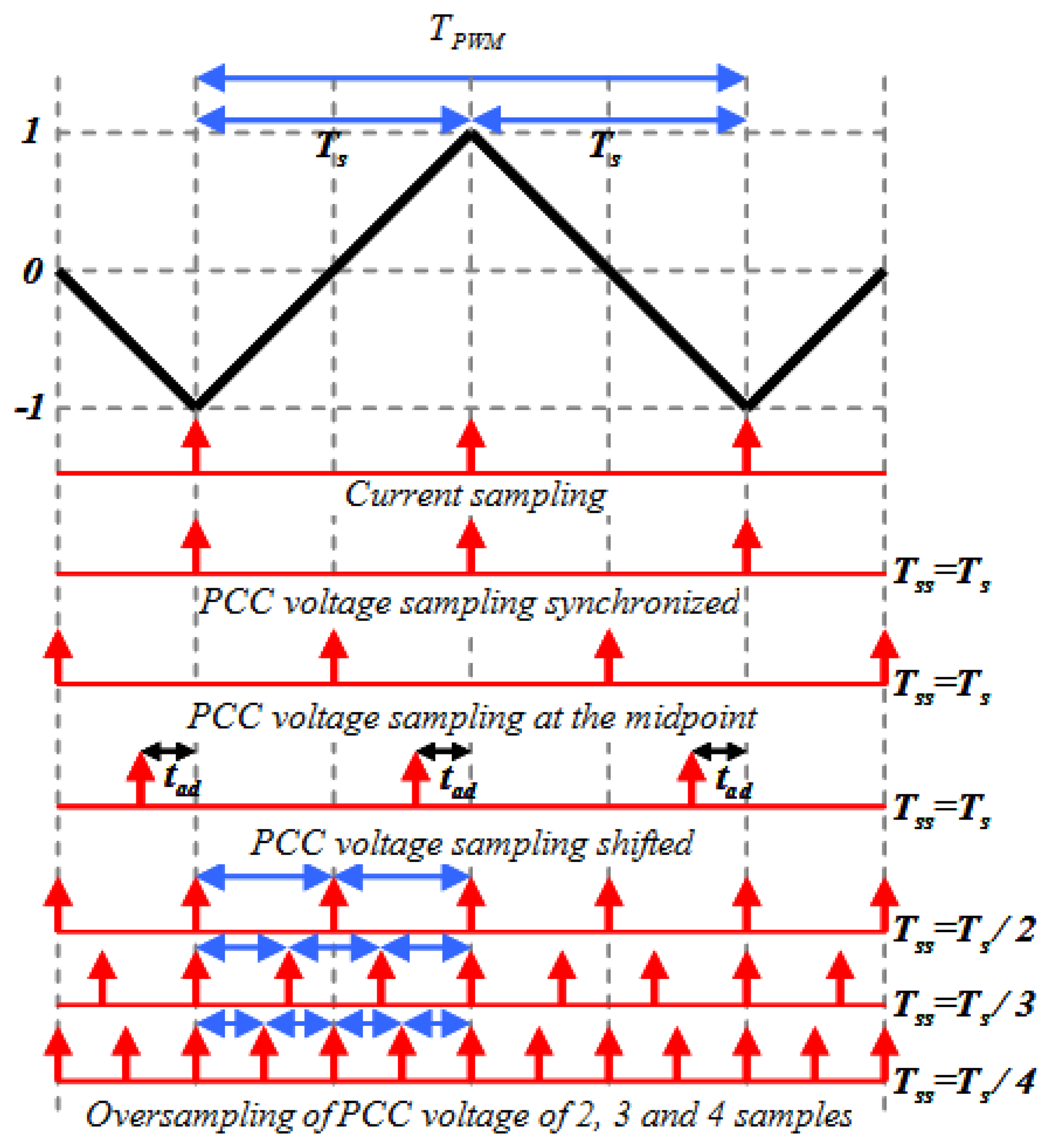
The methods studied here for sampling the PCC voltage are similar to those shown in [20]. With the system configuration defined in Table 1, several methods for performing the PCC voltage sampling are shown in Figure 11 [21]:
- (a)
The previously mentioned sampling method synchronized with the current sampling, where the sampling period of the PCC voltage and the timer, Tss, is equal to Ts (Figure 12a);
- (b)
Sampling at the midpoint of Ts, with Tss = Ts, which obtains a PCC voltage in dq-axes higher than the real value (Figure 12b);
- (c)
Sampling shifted a time tad with respect to the sampling instants of the current, where Tss = Ts and where the voltage remains erroneous (Figure 12c, where tad = Ts/4);
- (d)
Oversampling of two samples, synchronized with Ts, where Tss = Ts/2 and for which the voltage remains slightly erroneous (Figure 12d);
- (e)
Oversampling of three samples, synchronized with Ts, where Tss = Ts/3 and for which the voltage still remains slightly erroneous (Figure 12e), and
- (f)
Oversampling of four samples, which obtains a correct PCC voltage in dq-axes (Figure 12f).
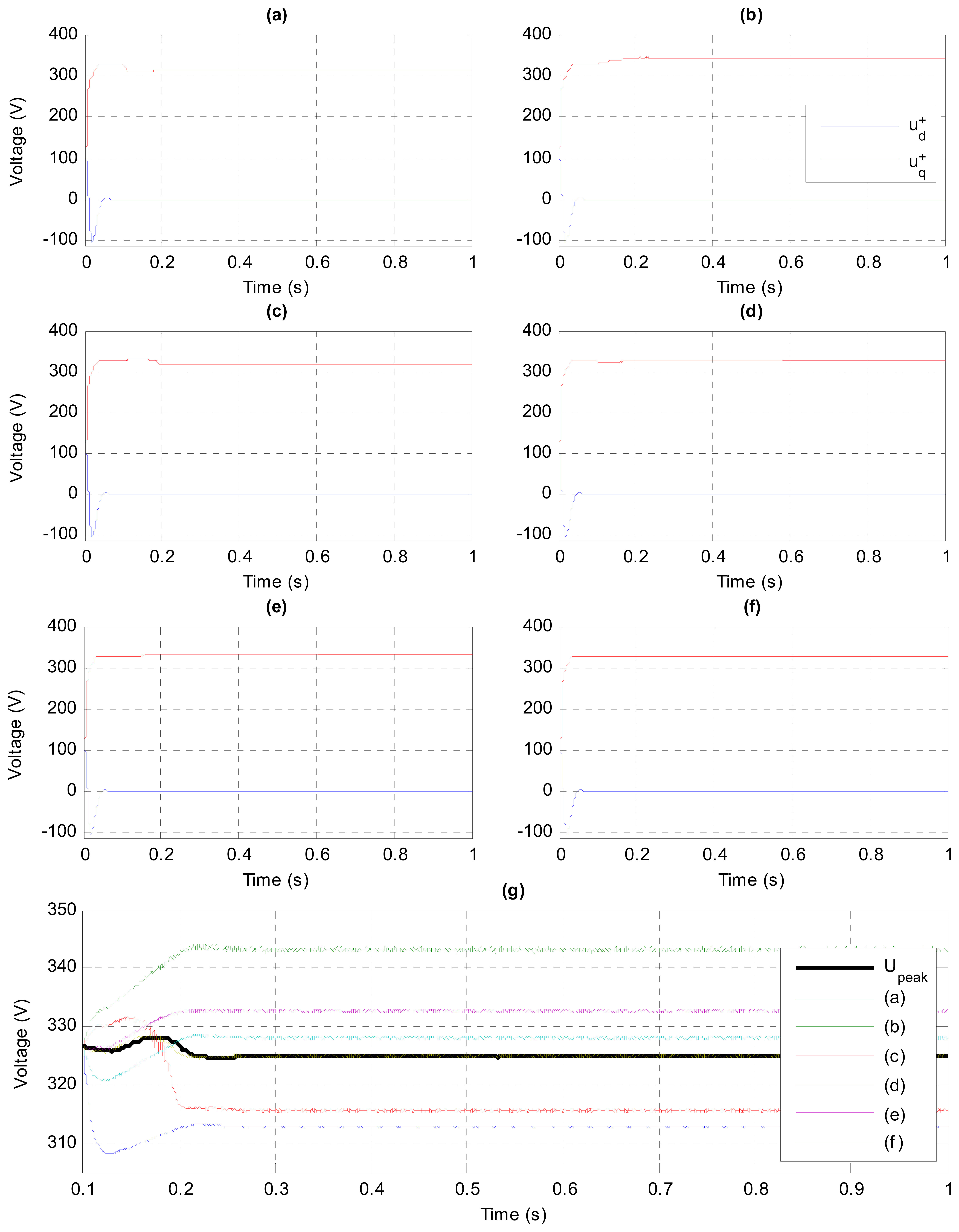
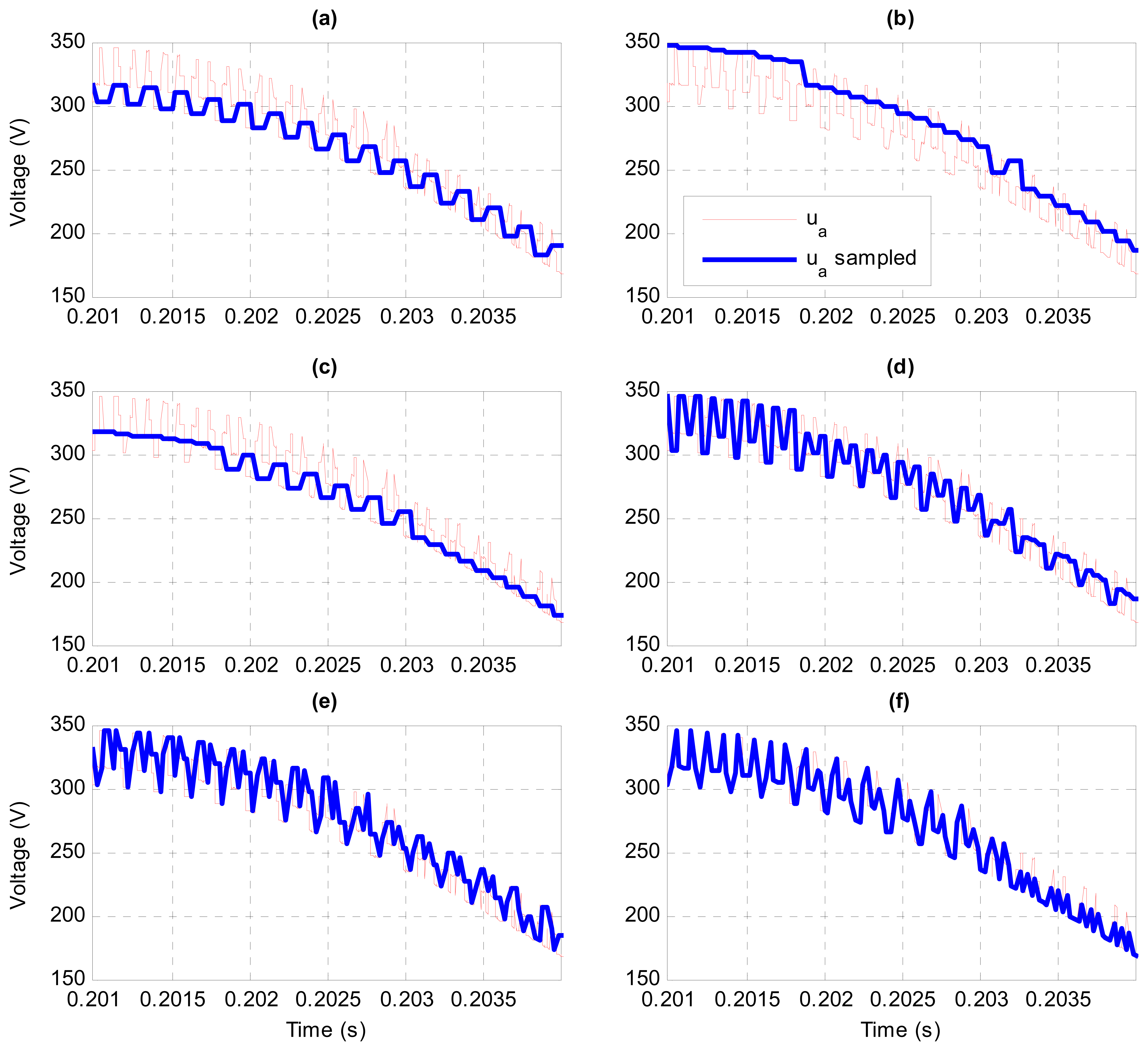
The estimated ( ) in steady-state with the six methods mentioned above are compared with the peak value of the fundamental PCC voltage in Figure 12g. Figure 13 shows the effect of applying each sampling method on the a-phase of the PCC voltage. It is straightforward to see the relationship between Figures 12g and 13:
Methods (a) and (c) detect an inner envelope of u, giving . Besides, the envelope detected with method (c) is the one closest to the fundamental voltage and, thus, ;
Method (b) detects an outer envelope of u, yielding ;
Methods (d) and (e) perform a more precise detection of the PCC voltage than methods (a) to (c), although there is still a small steady-state error. It is also observed that in spite of using a higher oversampling, which is due to the sampling at highly-noisy points of u;
Method (f), i.e., oversampling of four samples synchronized with Ts, is the only method that performs a precise detection of the PCC fundamental voltage:
The initial transient in the estimation of (Figure 12a–f) is due to the stabilization process of the PLL. However, this transient is not significant from the viewpoint of control performance because the converter control system only starts when the PLL is stable.
6. Simulation Results
6.1. Weak Grid Without Harmonics
A simulation has been carried out with MATLAB/Simulink® in order to test the performance of the proposed voltage controller. The ideal grid voltage of Figure 2 has been considered, along with the system parameters of Table 1. The NPC rated power is 100 kVA and the DC-link capacitors have a value of CDC1 = CDC2 = 4.5 mF. No load is connected to the PCC. The proposed voltage controller is enabled at t = 0.5 s.
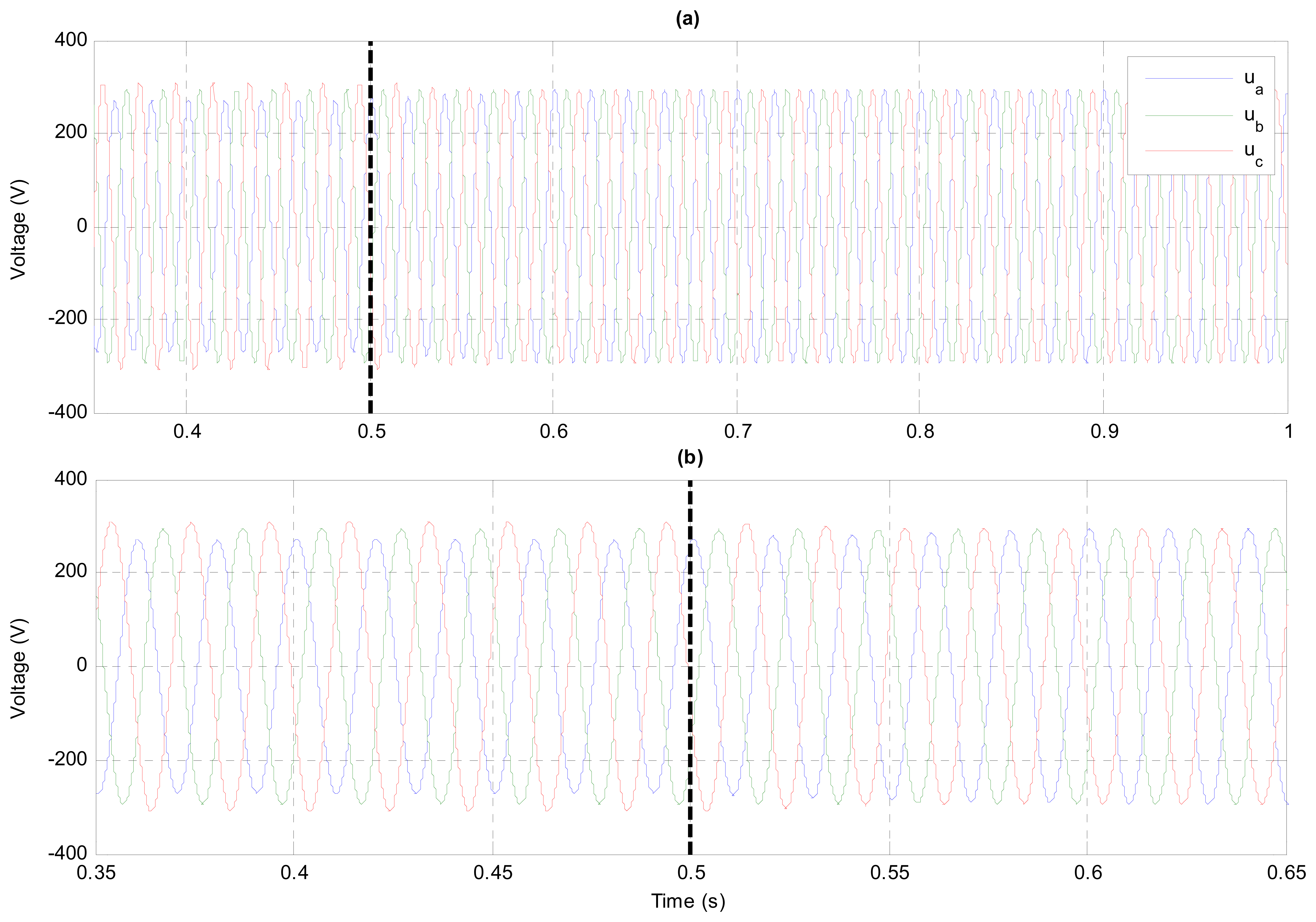
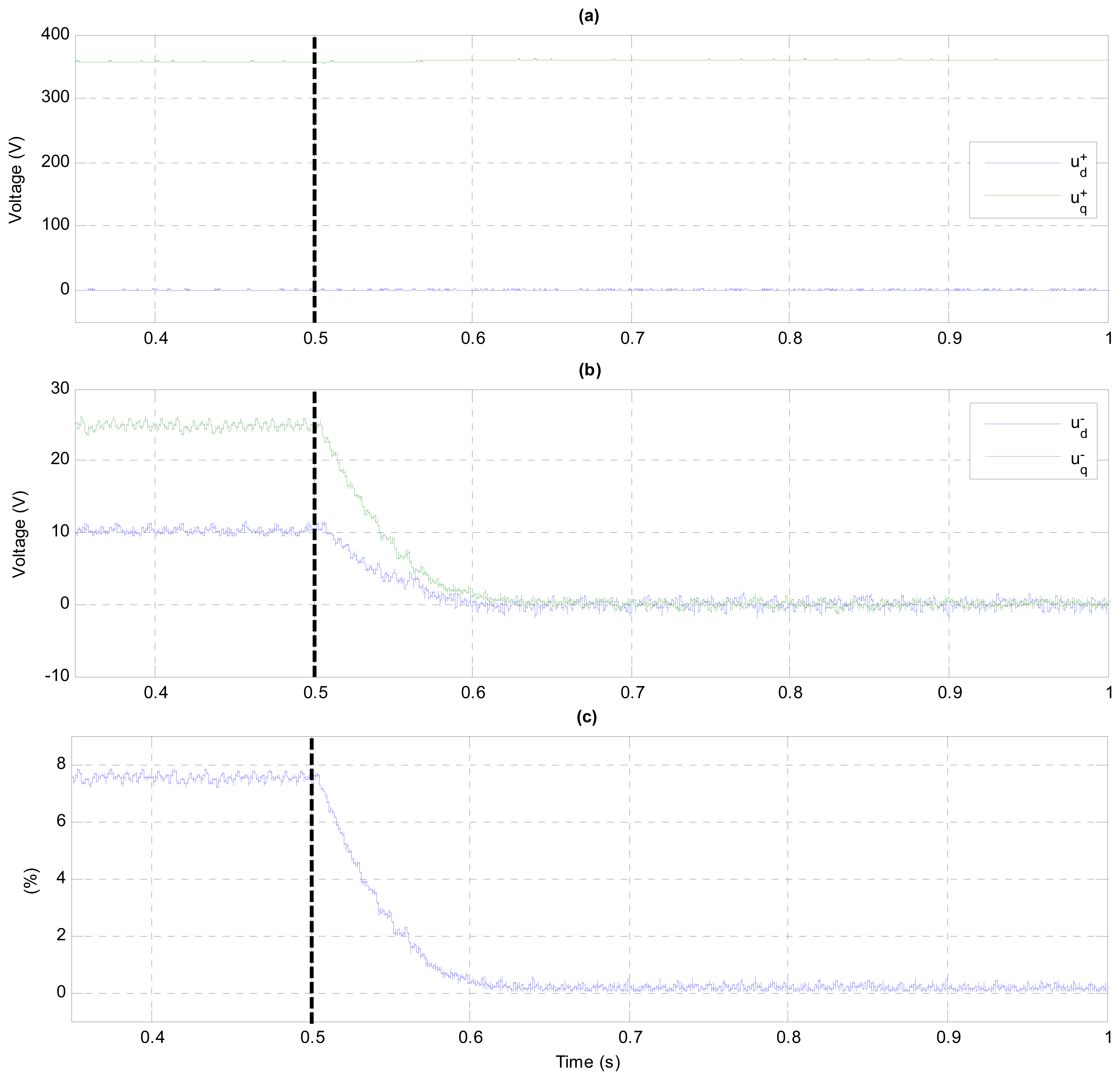
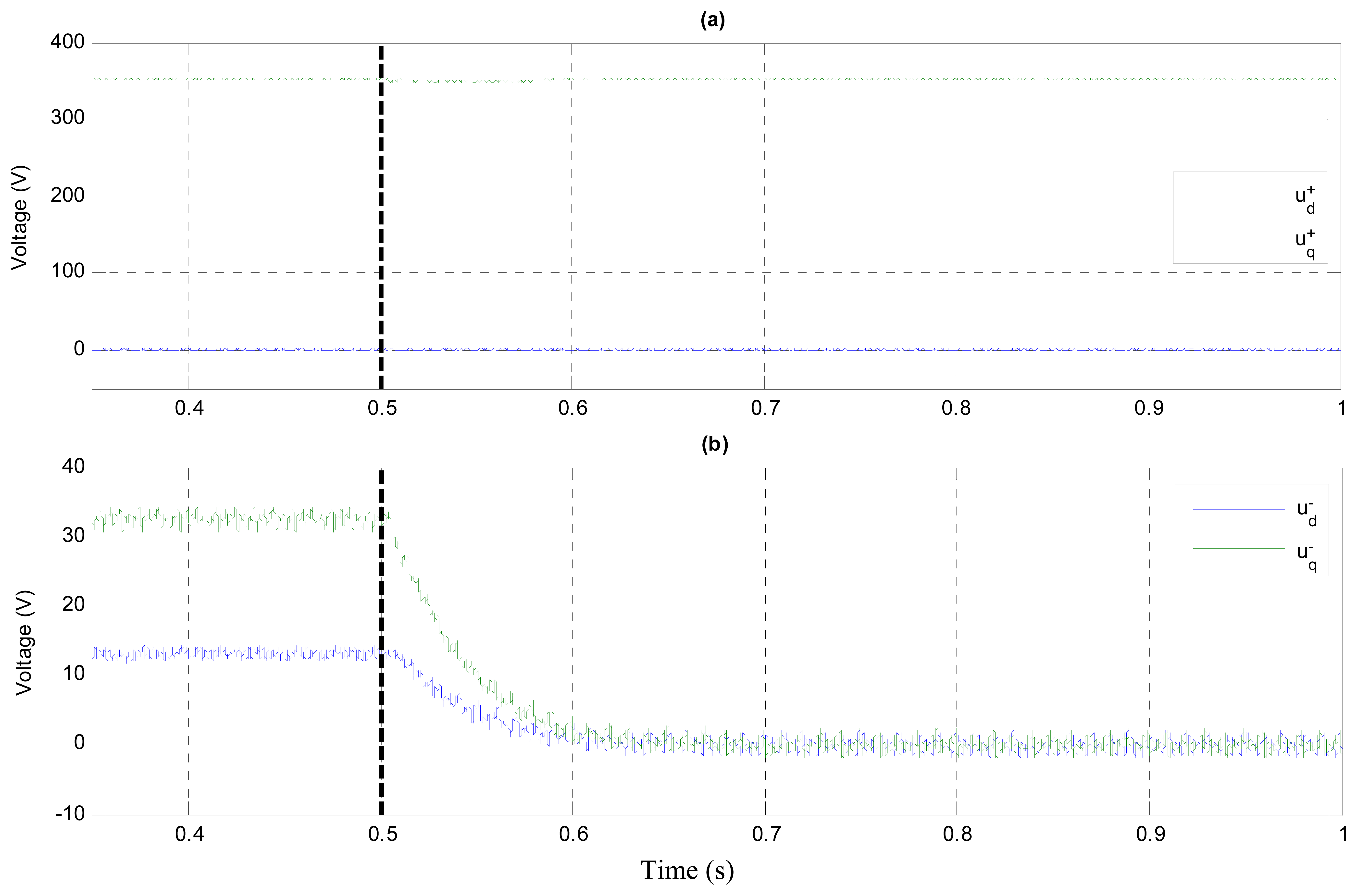
Figure 14 shows the temporary evolution of the filtered PCC voltage in abc-axes. Its non-filtered waveform presents a high ripple due to the high grid impedance and, in order to appreciate the effect of the PCC voltage controller, its filtered waveform is the one represented. In the following figures, the corresponding control activation time is marked with a dashed black line. It is clear that, when the voltage control is enabled, the PCC voltage is balanced. This is corroborated by decomposing this voltage in their positive and negative sequences as shown in Figure 15. The positive sequence remains equal because its reference voltage corresponds to the value it had before enabling the PCC voltage control. The negative sequence becomes almost zero since its reference voltage is set to zero for both d and q components, as well as the VUF.
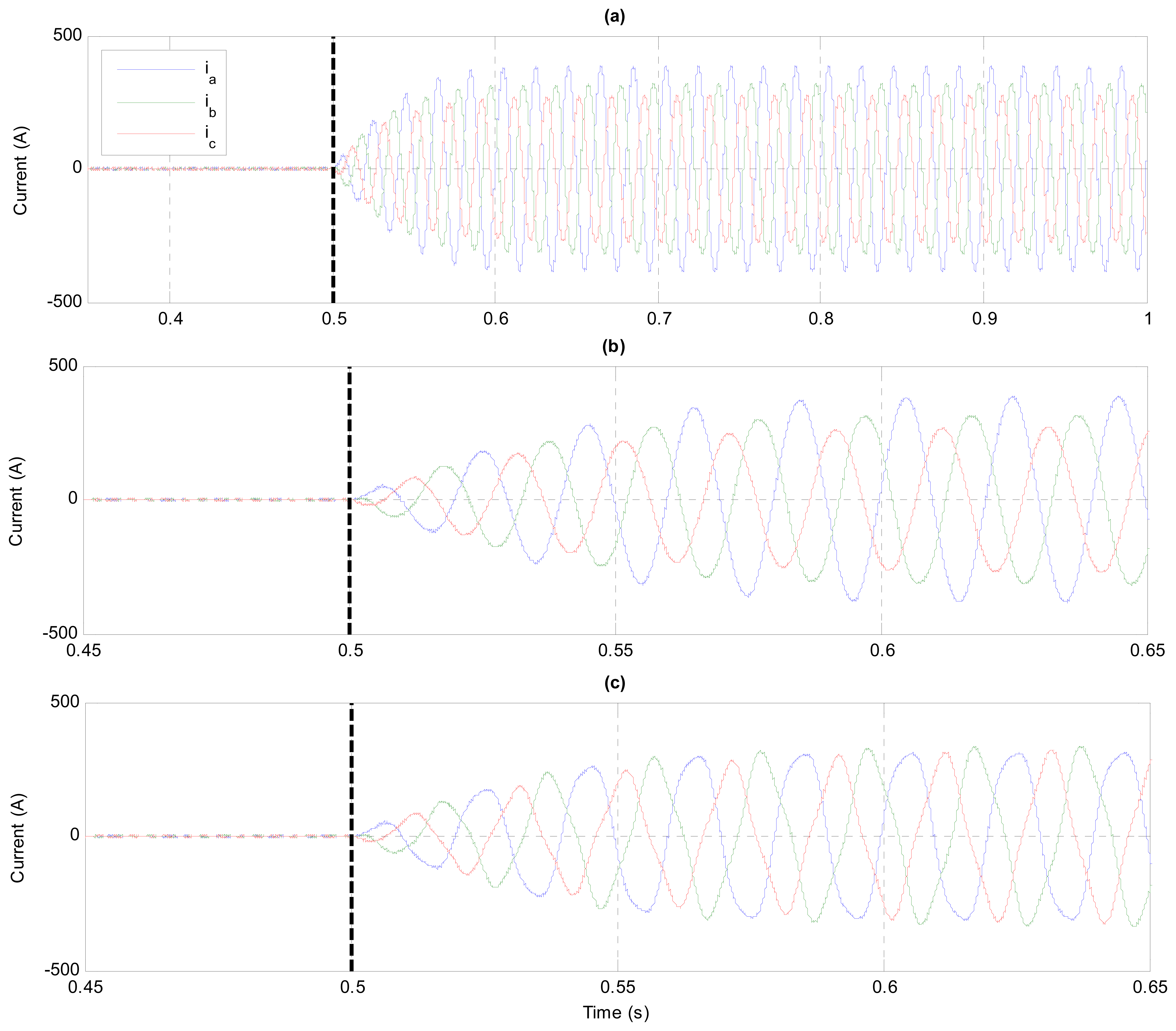
The current flowing from the VSC to the grid is represented in Figure 16a in abc-axes. Since no load is connected to the PCC, the current before enabling the voltage control is zero. Afterwards, the VSC provides an unbalanced current in order to compensate the negative sequence component. This is better observed in Figure 16b, which is a representation of Figure 16a between t = [0.45 0.65] s. Figure 16c is the equivalent of Figure 16b if the resonant controller 2ω is not included in the DC-link voltage controller, showing a PCC current with a 3rd order harmonic.
Since the PCC voltage is no longer unbalanced due to the effect of the voltage controller, the unbalance now appears in uDC. Figure 17a shows that a large oscillation appears in uDC, reaching nearly ±150 V. Besides, the DC-link voltage unbalance, calculated as the difference between positive and negative DC-link voltages (uDC1 − uDC2), also increases. If the oscillation level is not permissible, the reference for the negative sequence voltage can be set with a value different from zero but still low enough to satisfy regulations when it comes to maximum PCC voltage unbalance. In any case, it is worth remembering that the high level of unbalance applied to carry out these tests is usually not found in a real power system, so that in practice the amplitude of the oscillation will be much smaller. According to current regulations, a VUF greater than 2% in the worst case (e.g., IEC 61000-3-13 regulation) and 3% in the best case (e.g., ENTSO-E regulation) requires the disconnection of the converter from the grid, which can be avoided with the proposed PCC voltage controller.
6.2. Weak Grid With 5th and 7th Order Harmonics and a Higher Level of Negative Sequence
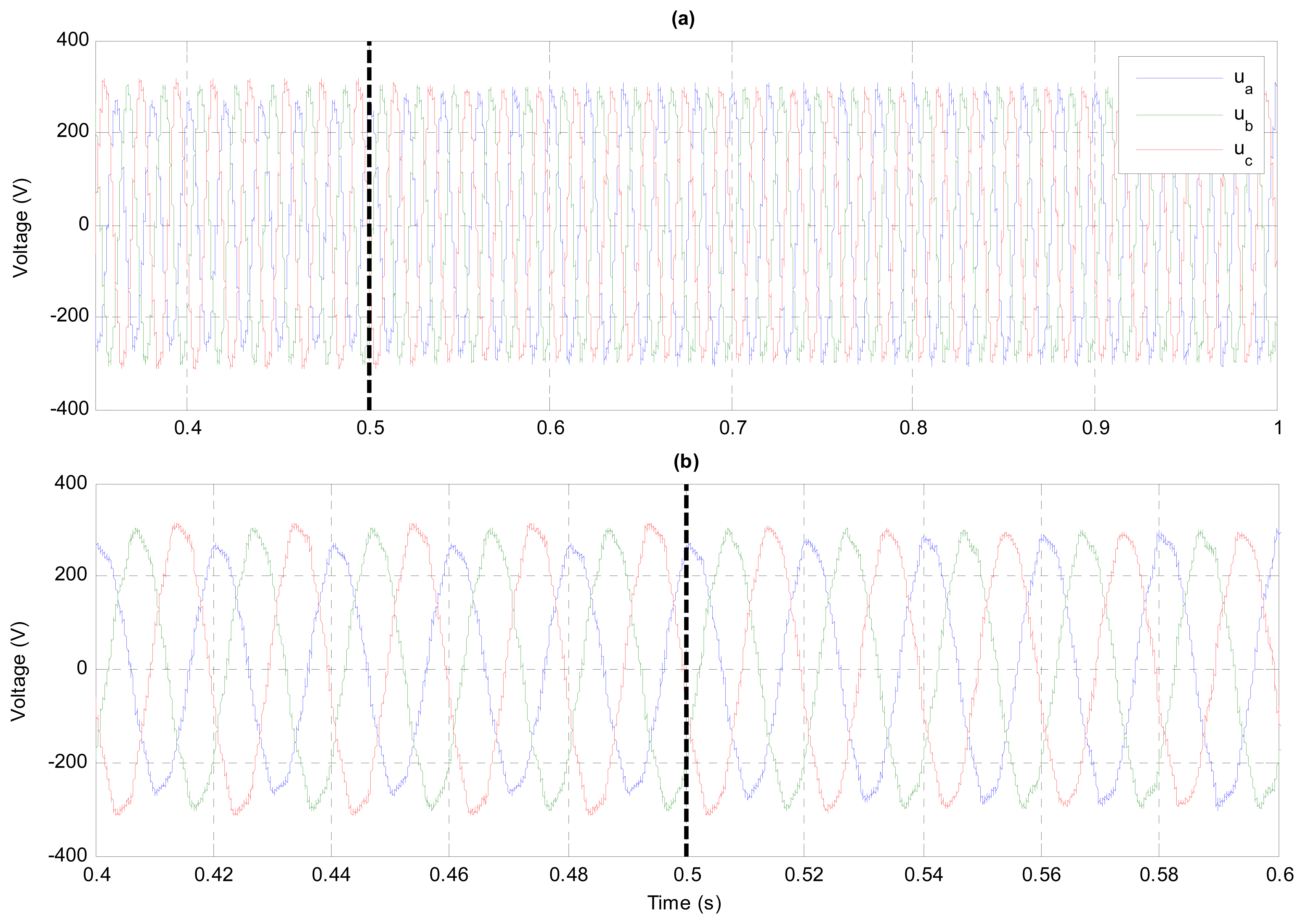
In order to test the performance of the proposed PCC voltage controller in a more realistic situation, 5th and 7th order harmonics have been included in the grid voltage with a level of A5 = 0.01 · A1 and A7 = 0.03 · A1, respectively. Furthermore, a higher level of negative sequence has been chosen (VUF = 10%). Figure 18 shows the temporal evolution of the PCC voltage waveform, validating as well the proper operation of the PCC voltage controller by compensating its negative sequence. The performance of the proposed controller is also observed in Figure 19, which collects the evolution of (Figure 19a), (Figure 19b) and the VUF (Figure 19c).
7. Conclusions
This article has proposed a PCC voltage controller in synchronous reference frame to compensate an unbalanced PCC voltage by means of a STATCOM, allowing an independent control of both positive and negative voltage sequences. To do so, the grid model has been studied under unbalanced conditions, showing the equations that relate voltage and current.
This voltage controller has been placed inside a control scheme to evaluate its performance by means of simulation results. These results have demonstrated the efficacy of this controller, managing to significantly reduce the oscillation present in the DC-link voltage.
However, due to the compensation of the PCC voltage negative sequence, an oscillation appears on the DC-link voltage, with frequency twice the fundamental grid frequency. The magnitude of this oscillation depends on the level of negative sequence. If the level of this oscillation is not permissible, the voltage reference for negative sequence voltage can be set with a value different from zero but still low enough to satisfy regulations when it comes to maximum PCC voltage unbalance. This would result in a reduction of uDC oscillation and DC-link voltage unbalance.
Experimental results have not been provided because the grid at our laboratory is not a weak grid and, even though this could be simulated by increasing the inductance in series with the VSC (thus, increasing the grid impedance), our three-level NPC converter has not been sized for compensating such unbalances.
Acknowledgments
This work has been funded by the Spanish Ministry of Economy and Competitiveness; projects ENE2011-28527-C04-01 and ENE2011-28527-C04-02.
Conflicts of Interest
The authors declare no conflict of interest.
References
- Piwko, R.; Miller, N.; Sánchez-Gasca, J.; Yuan, X.; Dai, R.; Lyons, J. Integrating Large Wind Farms into Weak Power Grids with Long Transmission Lines. Proceedings of Transmission and Distribution Conference and Exhibition: Asia and Pacific, 2005 IEEE/PES, Dalian, China; 2005; pp. 1–7. [Google Scholar]
- Ledesma, P.; Usaola, J.; Rodríguez, J.L. Transient stability of a fixed speed wind farm. Renew. Energy 2003, 28, 1341–1355. [Google Scholar]
- Farias, M.F.; Battaiotto, P.E.; Cendoya, M.G. Wind Farm to Weak-Grid Connection Using UPQC Custom Power Device. Proceedings of the IEEE International Conference on Industrial Technology (ICIT'10), Vi a del Mar, Chile, 14–17 March 2010; pp. 1745–1750.
- Yazdani, A.; Iravani, R. Voltage-Sourced Converters in Power Systems: Modeling, Control, and Applications; Wiley: Hoboken, NJ, USA, 2010. [Google Scholar]
- Schauder, C.; Gernhardt, M.; Stacey, E.; Lemak, T.; Gyugyi, L.; Cease, T.W.; Edris, A. Operation of ±100 MVAr TVA STATCON. IEEE Trans. Power Deliv. 1997, 12, 1805–1811. [Google Scholar]
- Bollen, M.H.J. Understanding Power Quality Problems—Voltage Sags and Interruptions; Wiley IEEE Press: New York, NY, USA, 2000. [Google Scholar]
- Pillay, P.; Manyage, M. Definitions of voltage unbalance. IEEE Power Eng. Rev. 2001, 22, 50–51. [Google Scholar]
- Akagi, H.; Watanabe, E.H.; Aredes, M. Instantaneous Power Theory and Applications to Power Conditioning; Wiley-IEEE Press: Hoboken, NJ, USA, 2007. [Google Scholar]
- Lee, C. Effects of unbalanced voltage on the operation performance of a three-phase induction motor. IEEE Trans. Energy Convers. 1999, 14, 202–208. [Google Scholar]
- Kang, J.; Sul, S. Control of Unbalanced Voltage PWM Converter Using Instantaneous Ripple Power Feedback. Proceedings of the 28th Annual IEEE Power Electronics Specialists Conference (PESC'97), St. Louis, MO, USA, 22–27 June 1997; pp. 503–508.
- Rodríguez, P.; Teodorescu, R.; Candela, I.; Timbus, A.V.; Liserre, M.; Blaabjerg, F. New Positive-Sequence Voltage Detector for Grid Synchronization of Power Converters under Faulty Grid Conditions. Proceedings of the 37th Annual IEEE Power Electronics Specialists Conference (PESC'06), Jeju, Korea, 18–22 June 2006; pp. 1–7.
- Ottersten, R. On Control of Back-to-Back Converters and Sensorless Induction Machine Drives. Ph.D. Thesis, Chalmers University of Technology, Goteborg, Sweden, 2003. [Google Scholar]
- Hingorani, N.G.; Gyugui, L. Understanding FACTS: Concepts and Technology of Flexible AC Transmission Systems; Wiley-IEEE Press: Hoboken, NJ, USA, 2000. [Google Scholar]
- Bojoi, R.I.; Griva, G.; Bostan, V.; Guerriero, M.; Farina, F.; Profumo, F. Current control strategy for power conditioners using sinusoidal signal integrators in synchronous reference frame. IEEE Trans. Power Electron. 2005, 20, 1402–1412. [Google Scholar]
- Wu, B. High-Power Converters and AC Drives; Wiley-IEEE Press: Hoboken, NJ, USA, 2006. [Google Scholar]
- Pou, J.; Zaragoza, J.; Ceballos, S.; Saeedifard, M.; Boroyevich, D. A carrier-based PWM strategy with zero-sequence voltage injection for a three-level Neutral-Point-Clamped converter. IEEE Trans. Power Electron. 2012, 27, 642–651. [Google Scholar]
- Pou, J.; Zaragoza, J.; Rodriguez, P.; Ceballos, S.; Sala, V.M.; Burgos, R.P.; Boroyevich, D. Fast-processing modulation strategy for the Neutral-Point-Clamped converter with total elimination of low-frequency voltage oscillations in the neutral point. IEEE Trans. Ind. Electron. 2007, 54, 2288–2294. [Google Scholar]
- Cóbreces, S. Optimization and Analysis of the Current Control Loop of VSCs Connected to Uncertain Grids through LCL Filters. Ph.D. Thesis, University of Alcala, Madrid, Spain, March 2009. [Google Scholar]
- Blasko, V.; Kaura, V.; Niewiadomski, W. Sampling of discontinuous voltage and current signals in electrical drives: A system approach. IEEE Trans. Ind. Appl. 1998, 34, 1123–1130. [Google Scholar]
- Briz, F.; Díaz-Reigosa, D.; Degner, M.W.; García, P.; Guerrero, J.M. Current Sampling and Measurement in PWM Operated AC Drives and Power Converters. Proceedings of the 2010 International Power Electronics Conference (IPEC'10), Sapporo, Japan, 21–24 June 2010; pp. 2753–2760.
- Huerta, F.; Cóbreces, S.; Rodríguez, F.J.; Bueno, E.; Díaz, M.J. Estudio de la Estabilidad del Modelo Discreto de Rectificadores PWM en Función de la Discretización y el Muestreo. Proceedings of the Seminario Anual de Automática, Electrónica Industrial e Instrumentación (SAAEI'10), Bilbao, Spain, 7–9 July 2010; pp. 296–301, in Spanish.


| Parameter | Symbol | Value | Units |
|---|---|---|---|
| Base apparent power | Sbase | 100 | kVA |
| Base voltage | Un | V | |
| Fundamental pulsation | ω1 | 2π50 | rad/s |
| Grid-filter inductance | L | 0.2209 | p.u. |
| Grid-filter resistance | R | 0.0034 | p.u. |
| Grid-impedance inductance | Lg | 0.0736 | p.u. |
| Grid-impedance resistance | Rg | 0.0005 | p.u. |
| Switching period | Tsw | 200 | μs |
| Sampling period | Ts | 100 | μs |
© 2014 by the authors; licensee MDPI, Basel, Switzerland. This article is an open access article distributed under the terms and conditions of the Creative Commons Attribution license ( http://creativecommons.org/licenses/by/3.0/).
Share and Cite
Rodríguez, A.; Bueno, E.J.; Mayor, Á.; Rodríguez, F.J.; García-Cerrada, A. Voltage Support Provided by STATCOM in Unbalanced Power Systems. Energies 2014, 7, 1003-1026. https://doi.org/10.3390/en7021003
Rodríguez A, Bueno EJ, Mayor Á, Rodríguez FJ, García-Cerrada A. Voltage Support Provided by STATCOM in Unbalanced Power Systems. Energies. 2014; 7(2):1003-1026. https://doi.org/10.3390/en7021003
Chicago/Turabian StyleRodríguez, Ana, Emilio J. Bueno, Álvar Mayor, Francisco J. Rodríguez, and Aurelio García-Cerrada. 2014. "Voltage Support Provided by STATCOM in Unbalanced Power Systems" Energies 7, no. 2: 1003-1026. https://doi.org/10.3390/en7021003