
Direct Printing of 1-D and 2-D Electronically Conductive Structures by Molten Lead-Free Solder

Abstract
:1. Introduction
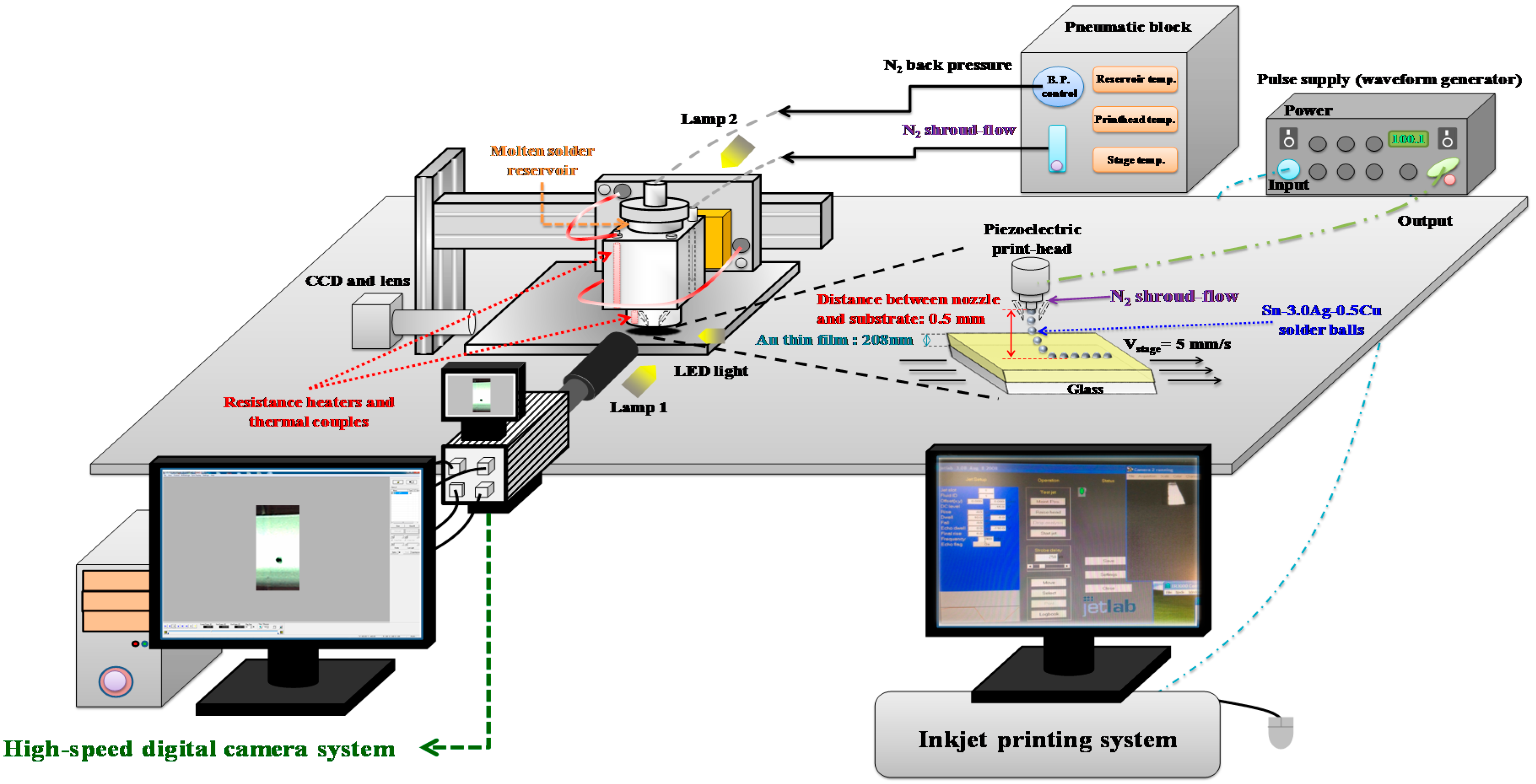
2. Experimental Methods
2.1. Apparatus and Method Description
2.2. Materials and Sample Preparation
2.3. Inkjet Printing Conditions
3. Results and Discussion
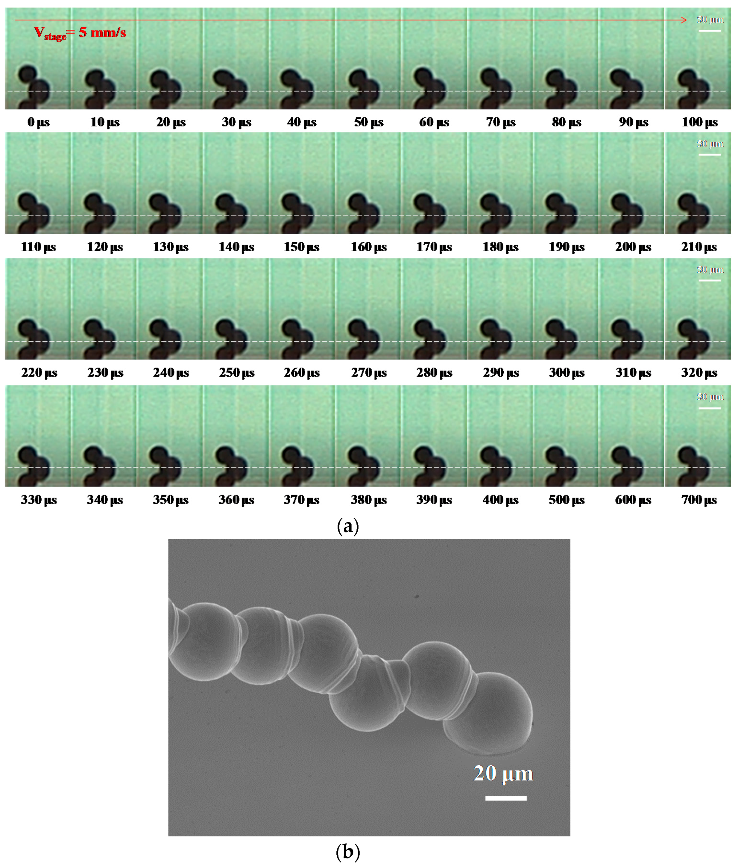
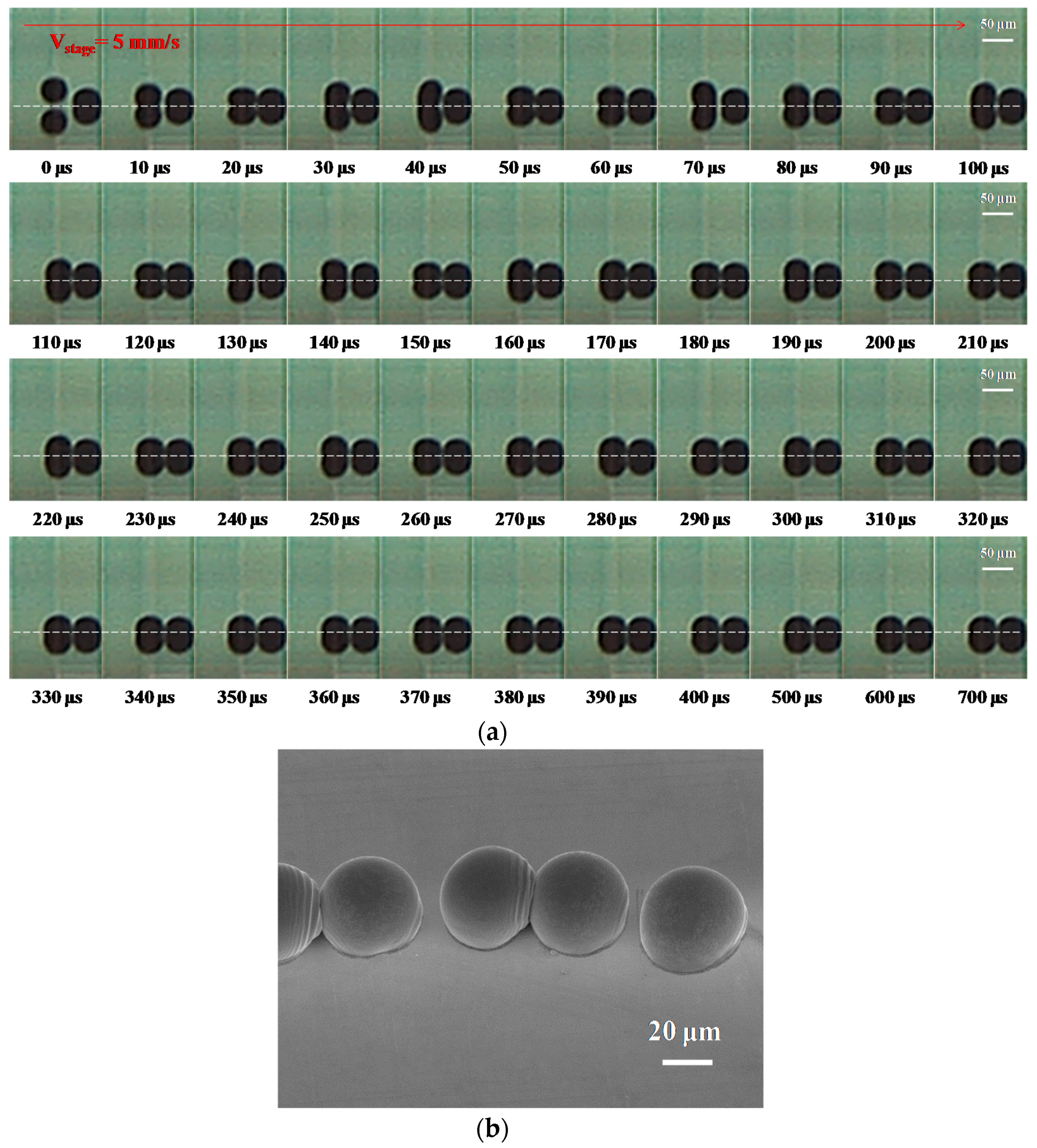
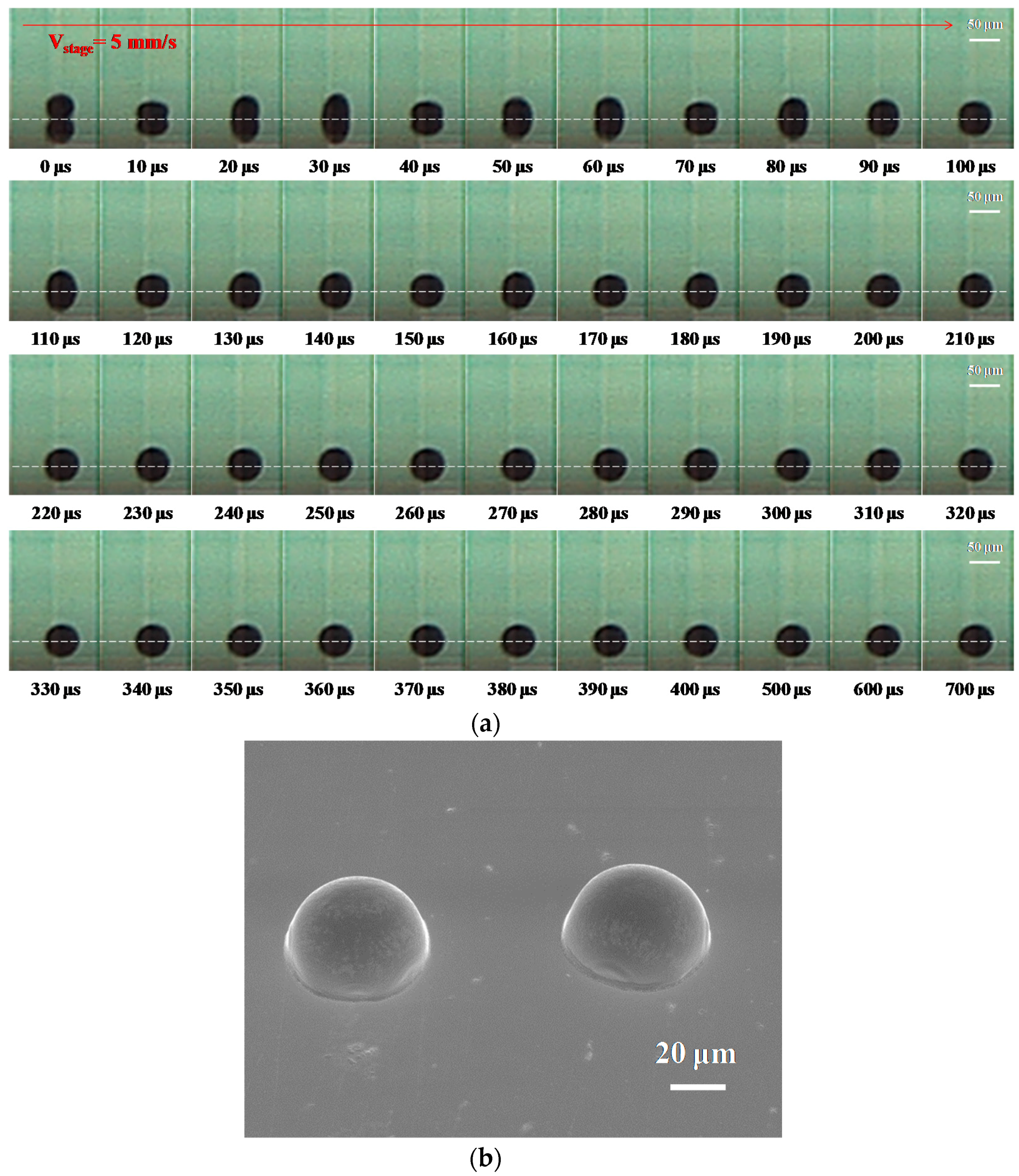
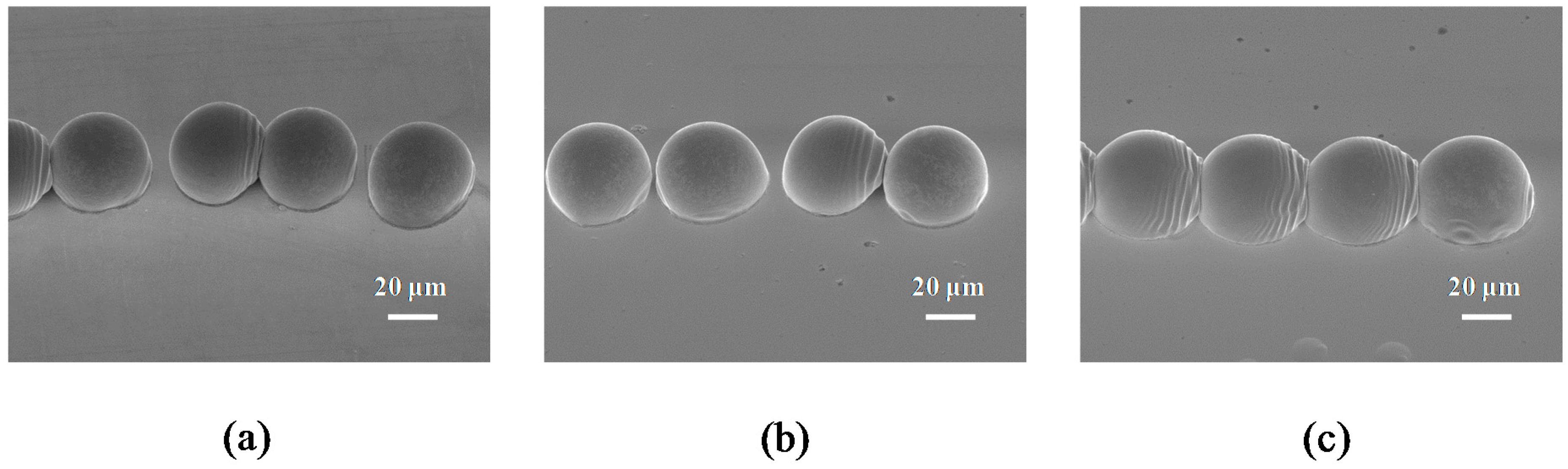
3.1. Effects of Dot Spacing on Droplet Formation and Deposition
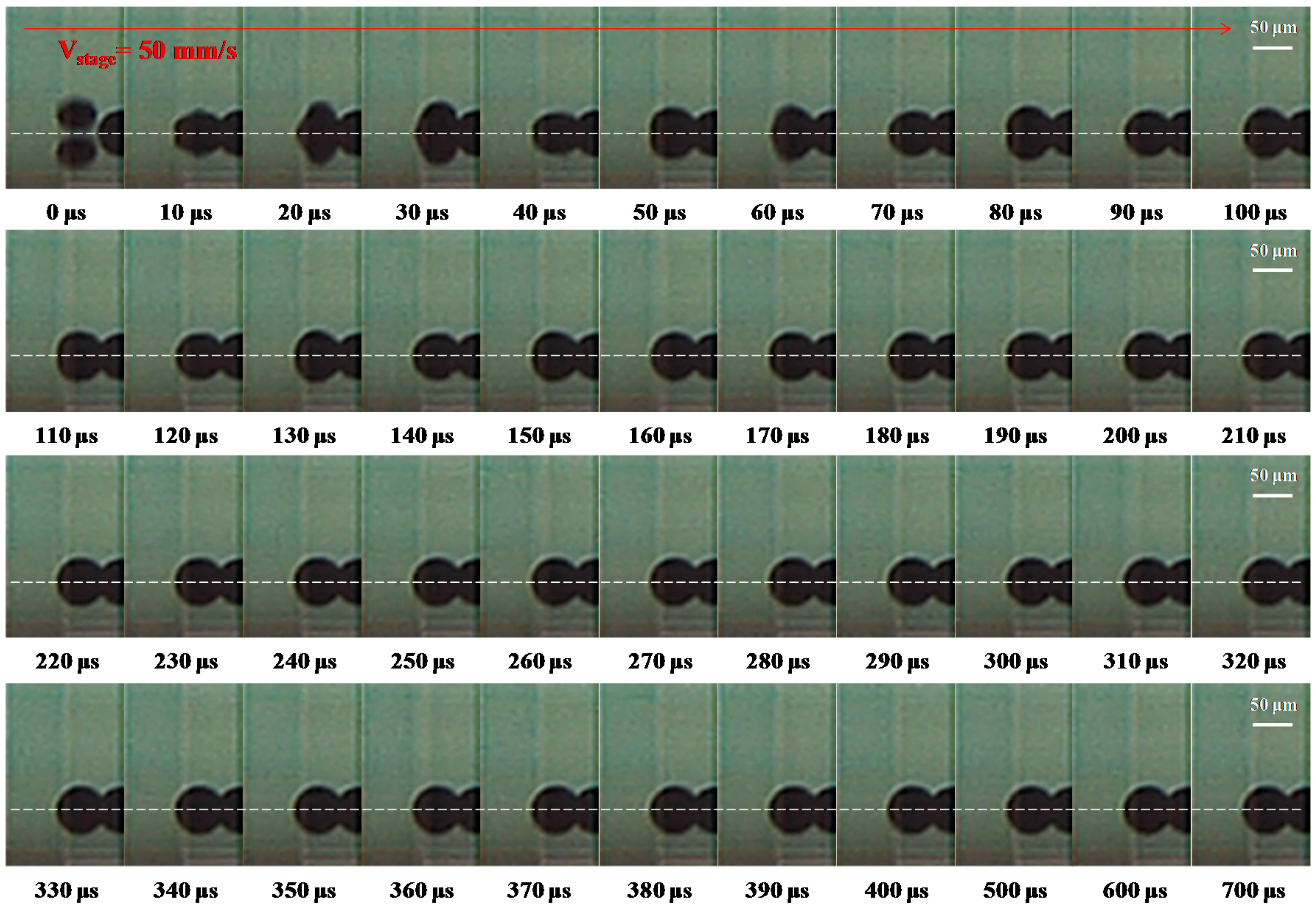
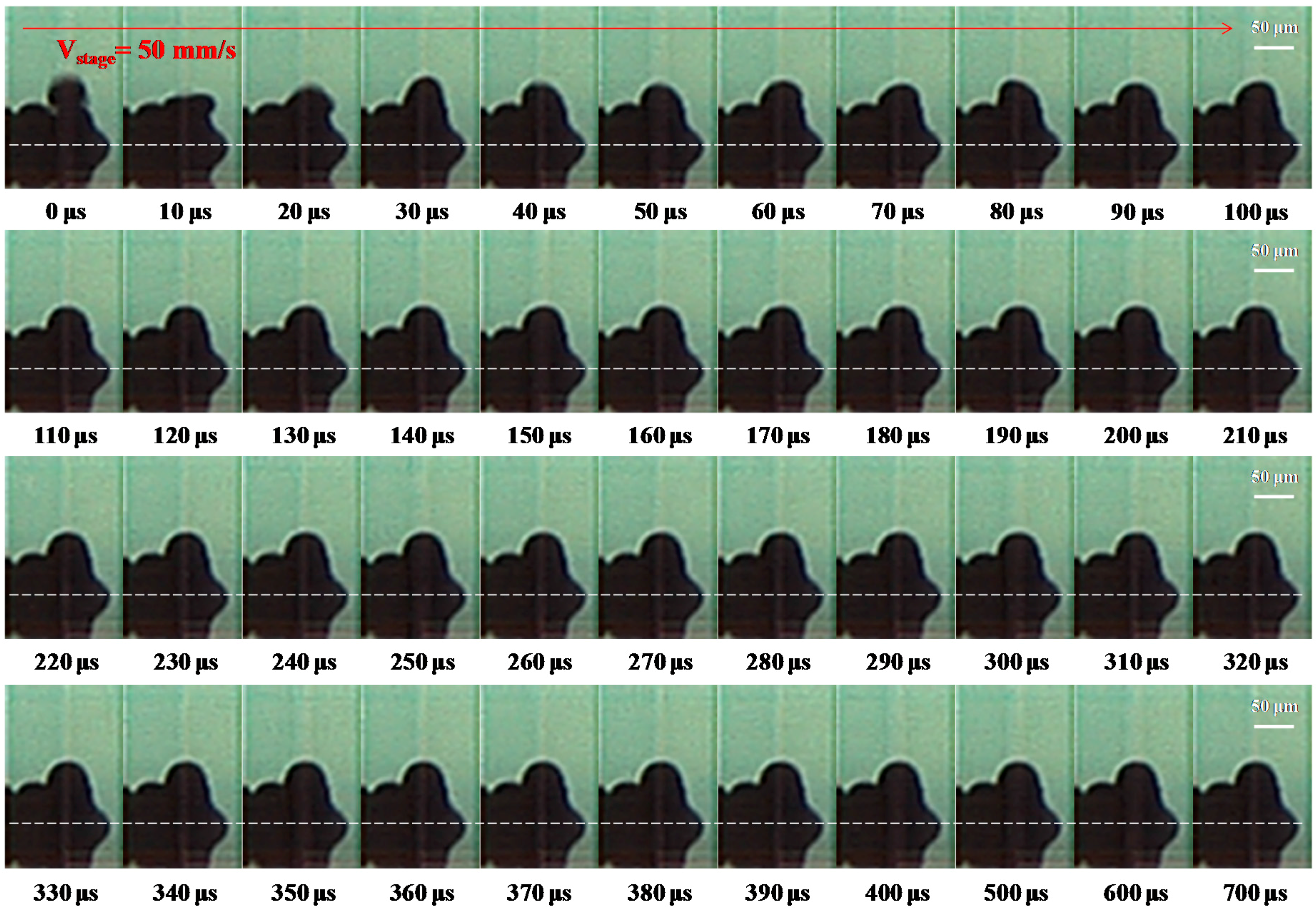
3.2. Effects of Motion Velocity on Droplet Formation and Deposition
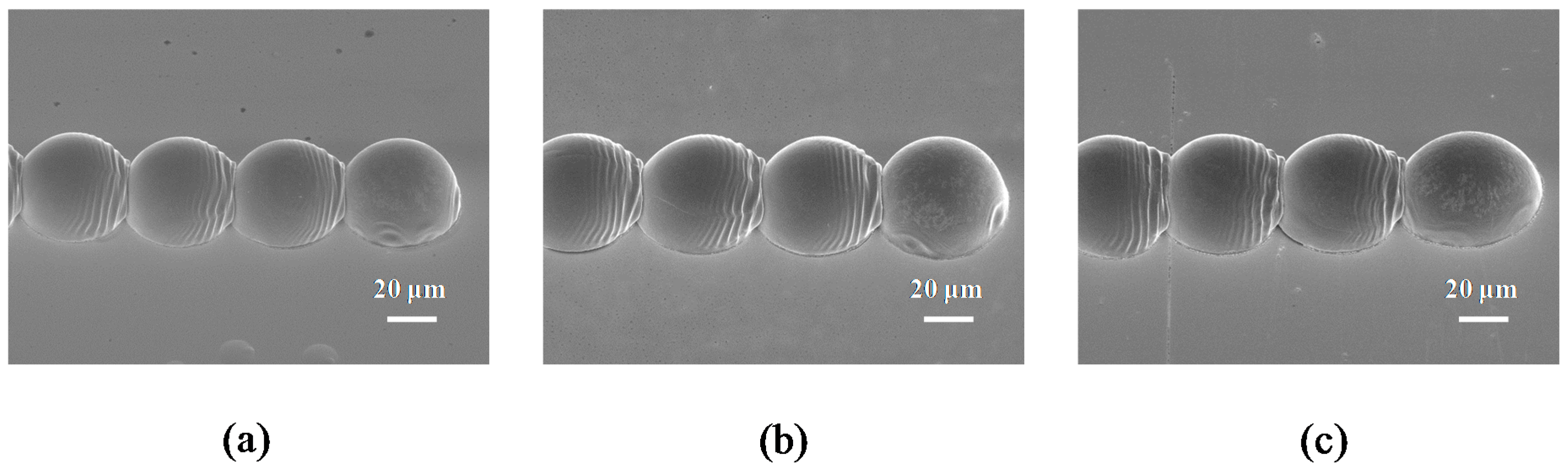
3.3. Study of the Deposition Process by Changing the Substrate Temperature
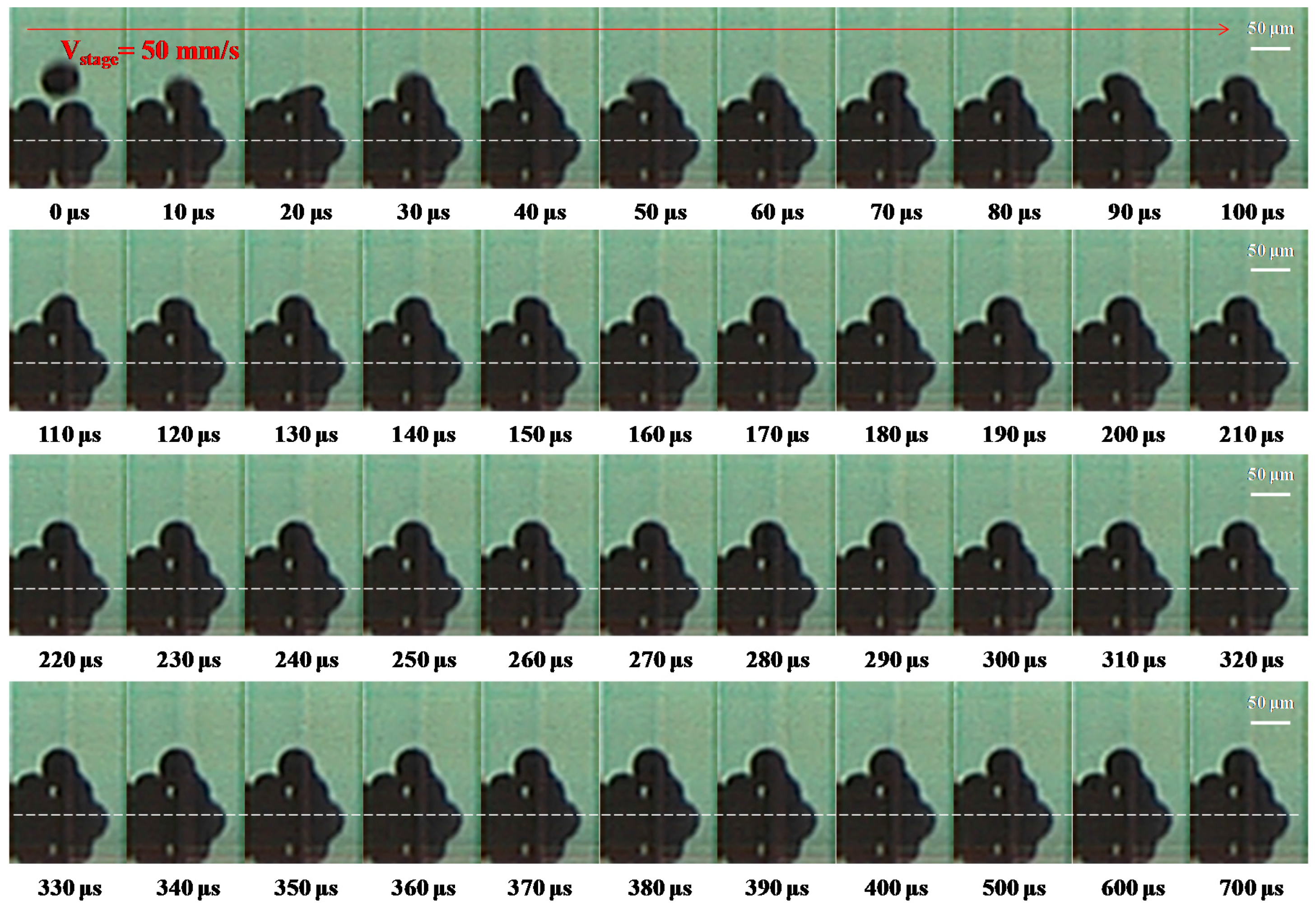
3.4. Formation of 2D Electronically Conductive Structures
4. Conclusions
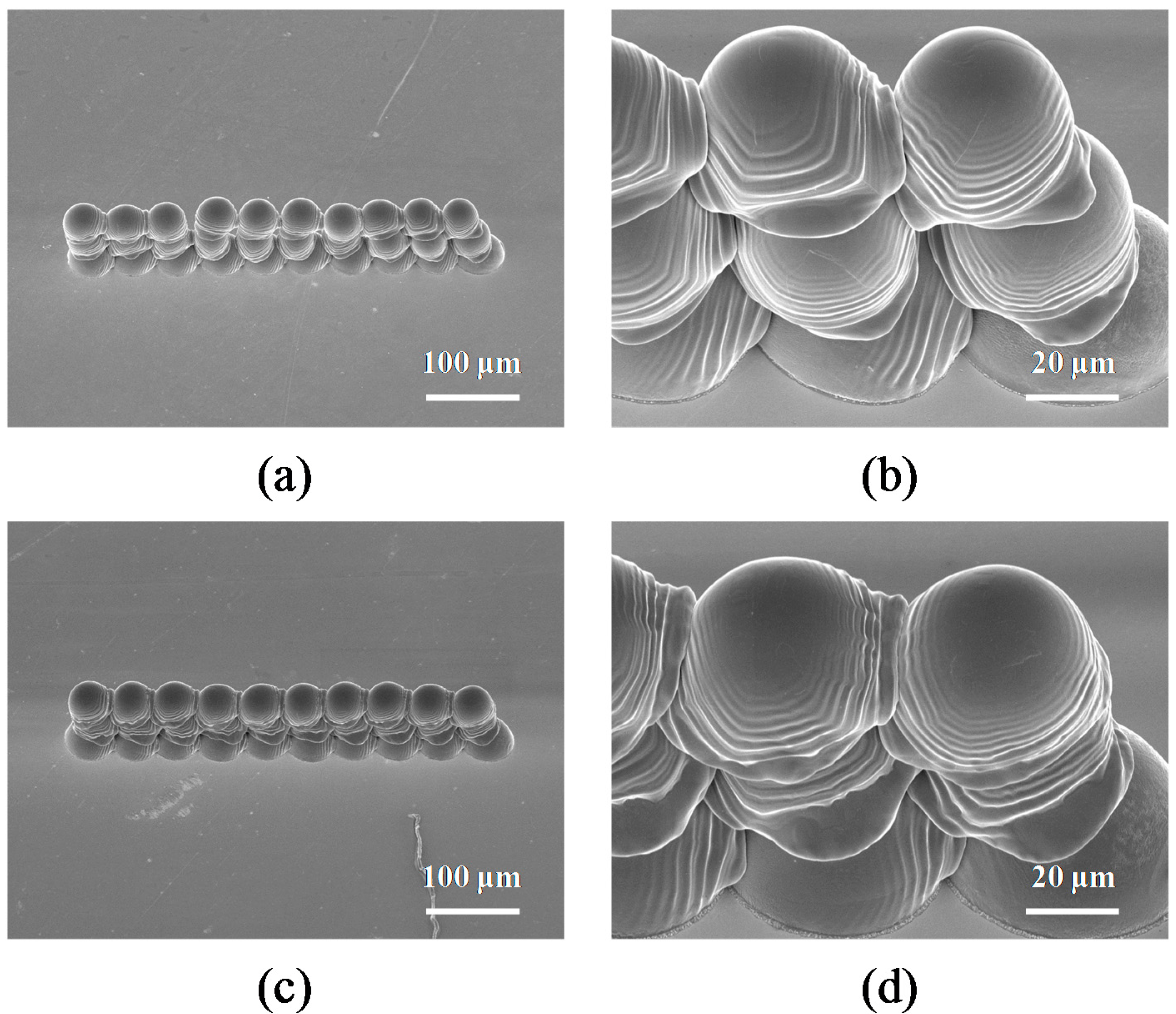
- The metallic line with a width of 55 μm can be successfully printed with respect to the value of the dot spacing (50 μm) and the stage velocity (50 mm∙s−1) at the substrate temperature of 30 °C. However, the L-shaped ridges of the lines on the solidified drop surface were formed for the time interval of 1 ms.
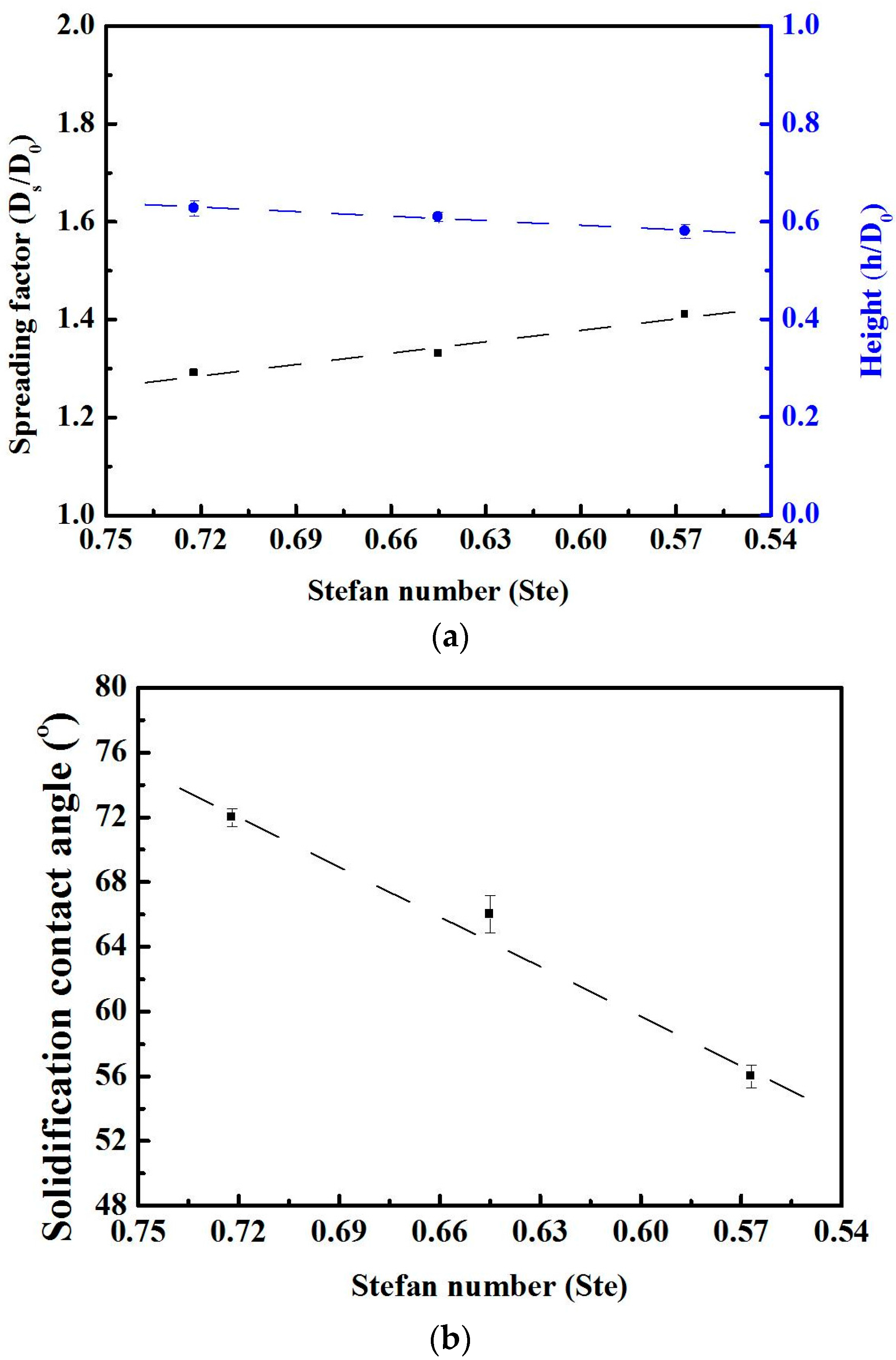
- With regard to the increase in sample temperature (from 30 to 70 °C), the height (from 0.63 to 0.58) and solidification contact angle (from 72° to 56°) of the metallic micro droplets gradually decreased on the substrate.
- The results of the SEM observations showed that the quality of 3D micro patterns improved significantly at 70 °C. The parallel lines of droplets were formed together with no visible micro pores on the interface between droplets.
Acknowledgments
Author Contributions
Conflicts of Interest
References
- Ko, S.H. Advanced inkjet technology for 3D micro-metal structure fabrication. In Micromanufacturing Engineering and Technology, 2nd ed.; Elsevier Inc.: Amsterdam, The Netherlands, 2015; pp. 425–439. [Google Scholar]
- Castrejon-Pita, J.R.; Baxter, W.R.S.; Morgan, J.; Temple, S.; Martin, G.D.; Hutchings, I.M. Future, opportunities and challenges of inkjet technologies. Atom. Sprays 2013, 23, 541–564. [Google Scholar] [CrossRef]
- Hayes, D.J.; Wallace, D.B.; Cox, W.R. Microjet printing of solder and polymers for multichip modules and chip-scale packages. In Proceedings of the IMAPS International Conference on High Density Packaging and MCMs, Denver, CO, USA, 6–9 April 1999; pp. 242–247.
- Wu, C.H.; Hwang, W.S. Study of solder jet bumping process using high-speed digital camera. Mater. Sci. Semicond. Process 2015, 31, 38–43. [Google Scholar] [CrossRef]
- Zenou, M.; Sa’ar, A.; Kotler, Z. Laser jetting of femto-liter metal droplets for high resolution 3D printed structures. Sci. Rep. 2015, 5, 17265. [Google Scholar] [CrossRef] [PubMed]
- Wang, C.H.; Tsai, H.L.; Wu, Y.C.; Hwang, W.S. Investigation of molten metal droplet deposition and solidification for 3D printing techniques. J. Micromech. Microeng. 2016, 26, 095012. [Google Scholar] [CrossRef]
- Lass, N.; Riegger, L.; Zengerle, R.; Koltay, P. Enhanced liquid metal micro droplet generation by pneumatic actuation based on the starJet method. Micromachines 2013, 4, 49–66. [Google Scholar] [CrossRef]
- Fuller, S.B.; Wilhelm, E.J.; Jacobson, J.M. Ink-jet printed nanoparticle microelectromechanical systems. J. Microelectromech. Syst. 2002, 11, 54–60. [Google Scholar] [CrossRef]
- Wallace, D.; Hayes, D.; Chen, T.; Shah, V.; Radulescu, D.; Cooley, P.; Wachtler, K.; Nallani, A. Think additive: Ink-jet deposition of materials for MEMS packaging. In Proceedings of the 6th Topical Workshop on Packaging of MEMS and Related Micro-Nano-Bio Integrated Systems, Long Beach, CA, USA, 18–20 November 2004; pp. 1–7.
- Luo, J.; Qi, L.H.; Tao, Y.; Ma, Q.; Visser, C.W. Impact-driven ejection of micro metal droplets on-demand. Int. J. Mach. Tools Manuf. 2016, 106, 67–74. [Google Scholar] [CrossRef]
- Fischer, A.C.; Mäntysalo, M.; Niklaus, F. Inkjet printing, laser-based micromachining and micro 3D printing technologies for MEMS. In Handbook of Silicon Based MEMS Materials and Technologies, 2nd ed.; Elsevier Inc.: Amsterdam, The Netherlands, 2015; pp. 550–564. [Google Scholar]
- Gale, B.K.; Eddings, M.A.; Sundberg, S.O.; Hatch, A.; Kim, J.K.; Ho, T. Low-cost MEMS technologies. Compr. Microsyst. 2008, 1, 341–378. [Google Scholar]
- Kim, H.Y.; Karahalios, T.; Qiu, T.; Chun, J.H. Microsensor for impact of molten metal microdrops. Sens. Actuator A Phys. 2004, 116, 417–423. [Google Scholar] [CrossRef]
- Jang, G.Y.; Duh, J.G. Elemental redistribution and interfacial reaction mechanism for the flip chip Sn-3.0Ag-(0.5 or 1.5) Cu solder bump with Al/Ni(V)/Cu under-bump metallization during aging. J. Electron. Mater. 2006, 35, 2061–2070. [Google Scholar] [CrossRef]
- Cooley, P.; Wallace, D.; Antohe, B. Applicatons of ink-jet printing technology to bioMEMS and microfluidic systems. J. Lab. Autom. 2002, 7, 33–39. [Google Scholar] [CrossRef]
- Ogawa, S.; Soda, S.; Lee, S.S.; Izuo, S.; Yoshida, Y. RF-MEMS switch with through-silicon via by the molten solder ejection method. Sens. Actuator A Phys. 2012, 181, 77–80. [Google Scholar] [CrossRef]
- Yokoyama, Y.; Endo, K.; Iwasaki, T.; Fukumoto, H. Variable-size solder droplets by a molten-solder ejection method. J. Microelectromech. Syst. 2009, 18, 316–321. [Google Scholar] [CrossRef]
- Tsai, M.H.; Hwang, W.S.; Chou, H.H. The micro-droplet behavior of a molten lead-free solder in an inkjet printing process. J. Micromech. Microeng. 2009, 19, 125021. [Google Scholar] [CrossRef]
- Li, H.J.; Wang, P.Y.; Qi, L.H.; Zuo, H.S.; Zhong, S.Y.; Hou, X.H. 3D numerical simulation of successive deposition of uniform molten Al droplets on a moving substrate and experimental validation. Comput. Mater. Sci. 2012, 65, 291–301. [Google Scholar] [CrossRef]
- Luo, J.; Qi, L.H.; Zhong, S.Y.; Zhou, J.M.; Li, H.J. Printing solder droplets for micro devices packages using pneumatic drop-on-demand (DOD) technique. J. Mater. Process. Technol. 2012, 212, 2066–2073. [Google Scholar] [CrossRef]
- Ristenpart, W.D.; McCalla, P.M.; Roy, R.V.; Stone, H.A. Coalescence of spreading droplets on a wettable substrate. Phys. Rev. Lett. 2006, 97, 064501. [Google Scholar] [CrossRef] [PubMed]
- Dong, H.; Carr, W.W.; Morris, J.F. Visualization of drop-on-demand inkjet: Drop formation and deposition. Rev. Sci. Instrum. 2006, 77, 085101. [Google Scholar] [CrossRef]
- Li, H.P.; Li, H.J.; Qi, L.H.; Luo, J.; Zuo, H.S. Simulation on deposition and solidification processes of 7075 Al alloy droplets in 3D printing technology. Trans. Nonferrous Met. Soc. China 2014, 24, 1836–1843. [Google Scholar] [CrossRef]
- Haferl, S.; Poulikakos, D. Experimental investigation of the transient impact fluid dynamics and solidification of a molten microdroplet pile-up. Int. J. Heat Mass Transf. 2003, 46, 535–550. [Google Scholar] [CrossRef]
- Du, J.; Wei, Z.Y.; Chen, Z.; Li, S.L.; Tang, Y.P. Numerical investigation of pile up process in metal microdroplet deposition manufacture. Micromachines 2014, 5, 1429–1444. [Google Scholar] [CrossRef]
- Otendal, M.; Hemberg, O.; Tuohimaa, T.T.; Hertz, H.M. Microscopic high-speed liquid-metal jets in vacuum. Exp. Fluids 2005, 39, 799–804. [Google Scholar] [CrossRef]
- Li, R.; Ashgriz, N.; Chandra, S. Maximum spread of droplet on solid surface: Low Reynolds and Weber numbers. Int. J. Therm. Sci. 2010, 132, 061302. [Google Scholar] [CrossRef]
- Gong, S.C. Spreading of droplets impacting on smooth solid surface. Jpn. J. Appl. Phys. 2005, 44, 3323–3324. [Google Scholar] [CrossRef]
- Le Bot, C.; Vincent, S.; Arquis, E. Impact and solidification of indium droplets on a cold substrate. Int. J. Therm. Sci. 2005, 44, 219–233. [Google Scholar] [CrossRef]
- Directive 2002/95/EC of the European Parliament and of the Council of 27 January 2003 on the Restriction of the Use of Certain Hazardous Substances in Electrical and Electronic Equipment (RoHS). Available online: http://eur-lex.europa.eu/LexUriServ/LexUriServ.do?uri=OJ:L:2003:037:0019:0023:EN:PDF (accessed on 4 October 2016).
- Handwerker, C. Transitioning to Pb-free assemblies. INEMI Rep. 2005. [Google Scholar]
- Nurmi, S.T.; Sundelin, J.J.; Ristolainen, E.O.; Lepisto, T.K. The effect of PCB surface finish on lead-free solder joints. Solder. Surf. Mt. Technol. 2005, 17, 13–23. [Google Scholar] [CrossRef]
- Abtew, M.; Selvaduray, G. Lead free solder in microelectron. Mater. Sci. Eng. R Rep. 2000, 27, 95–141. [Google Scholar] [CrossRef]
- Wong, E.H.; Rajoo, R.; Seah, S.K.W.; Selvanayagam, C.S.; van Driel, W.D.; Caers, J.F.J.M.; Zhao, X.J.; Owens, N.; Tan, L.C.; Leoni, M.; et al. Correlation studies for component level ball impact shear test and board level drop test. Microelectron. Reliab. 2008, 48, 1069–1078. [Google Scholar] [CrossRef]
- Tsai, K.T.; Liu, F.L.; Wong, E.H.; Rajoo, R. High strain rate testing of solder interconnections. Solder. Surf. Mt. Technol. 2006, 18, 12–17. [Google Scholar] [CrossRef]
- Islam, R.A.; Chan, Y.C.; Jillek, W.; Islam, S. Comparative study of wetting behavior and mechanical properties (microhardness) of Sn-Zn and Sn-Pb solders. Microelectron. J. 2006, 37, 705–713. [Google Scholar] [CrossRef]
- Bigas, M.; Cabruja, E. Characterisation of electroplated Sn/Ag solder bumps. Microelectron. J. 2006, 37, 308–316. [Google Scholar] [CrossRef]
- Ratchev, P.; Loccufier, T.; Vandevelde, B.; Teliszewski, S.; Werkhoven, D.; Allaert, B. A study of brittle to ductile fracture transition temperatures in bulk Pb-free solders. In Proceedings of the 15th European Microelectronics and Packaging Conference and Exhibition, Bruges, Belgium, 12–15 June 2005; pp. 248–252.
- Tian, D.W.; Wang, C.Q.; Tian, Y.H. Effect of solidification on solder bump formation in solder jet process: Simulation and experiment. Trans. Nonferrous Met. Soc. China 2008, 18, 1201–1208. [Google Scholar] [CrossRef]
- Park, J.; Kim, B.; Kim, S.Y.; Hwang, J. Prediction of drop-on-demand (DOD) pattern size in pulse voltage-applied electrohydrodynamic (EHD) jet printing of Ag colloid ink. Appl. Phys. A 2014, 117, 2225–2234. [Google Scholar] [CrossRef]
- Vincent, S.; Bot, C.L.; Sarret, F.; Meillot, E.; Caltagirone, J.P.; Bianchi, L. Penalty and eulerian–lagrangian VOF methods for impact and solidification of metal droplets plasma spray process. Comput. Fluids 2015, 113, 32–41. [Google Scholar] [CrossRef]
- Li, R. Droplet Deposition in Solid Ink Printing. Ph.D. Thesis, University of Toronto, Toronto, ON, Canada, 2008. [Google Scholar]
- Kim, I.; Kang, M.I.; Kim, S.W.; Jung, E.; Lee, S.H. Thermal diffusivity of Sn-Ag-Cu-based, Pb-free, micro- and nano-sized solder balls. Thermochim. Acta 2012, 542, 42–45. [Google Scholar] [CrossRef]
- Gao, F.; Sonin, A.A. Precise deposition of molten microdrops: The physics of digital microfabrication. Proc. R. Soc. A 1994, 444, 533–554. [Google Scholar] [CrossRef]


| Parameters | Value | Unit | Symbol |
|---|---|---|---|
| Density | 7500 | kg∙m−3 | ρ |
| Viscosity | 2 | mPa∙s | η |
| Surface tension coefficient | 0.431 | N∙m−1 | σ |
| Liquidus temperature | 221 | °C | θl |
| Solidus temperature | 216 | °C | θs |
| Specific heat of liquid | 250 | J∙kg−1∙°C−1 | Cp |
| Equilibrium freezing temperature of solder | 217 | °C | Tm |
| Latent heat of fusion | 64,762 | J∙kg−1 | L |
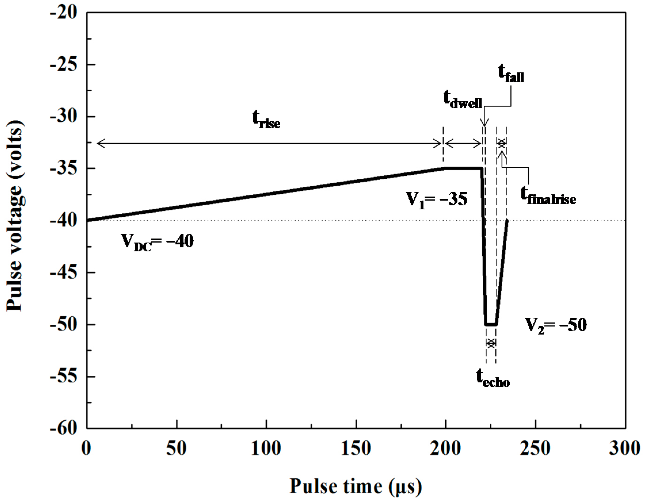
| Condition | Pulse Time (μs) | Drop Frequency (Hz) | Pulse Voltage (V) | Jet Height (mm) | Reservoir Pressure (kPa) | Sample Temperature (°C) | ||||||
|---|---|---|---|---|---|---|---|---|---|---|---|---|
| Trise | Tdwell | Tfall | Techo | Tfinalrise | VDC | V1 | V2 | |||||
| A | 200 | 20 | 2 | 6 | 6 | 200 | −40 | −35 | −50 | 0.5 | 1.0 | 30 |
| B | 200 | 20 | 2 | 6 | 6 | 100 | −40 | −35 | −50 | 0.5 | 1.0 | 30 |
| C | 200 | 20 | 2 | 6 | 6 | 50 | −40 | −35 | −50 | 0.5 | 1.0 | 30 |
| D | 200 | 20 | 2 | 6 | 6 | 1000 | −40 | −35 | −50 | 0.5 | 1.0 | 30 |
| E | 200 | 20 | 2 | 6 | 6 | 1000 | −40 | −35 | −50 | 0.5 | 1.0 | 50 |
| F | 200 | 20 | 2 | 6 | 6 | 1000 | −40 | −35 | −50 | 0.5 | 1.0 | 70 |
| Sample Temperature (°C) | Weber Number | Reynolds Number | Ohnesorge Number | Stefan Number | The Average Width of Metallic Line (μm) |
|---|---|---|---|---|---|
| 30 | 0.92 | 206.25 | 4.7 × 10⁻³ | 0.722 | 55 ± 1.3 |
| 50 | 0.92 | 206.25 | 4.7 × 10⁻³ | 0.645 | 56 ± 1.4 |
| 70 | 0.92 | 206.25 | 4.7 × 10⁻³ | 0.567 | 59 ± 1.7 |
© 2016 by the authors. Licensee MDPI, Basel, Switzerland. This article is an open access article distributed under the terms and conditions of the Creative Commons Attribution (CC-BY) license ( http://creativecommons.org/licenses/by/4.0/).
Share and Cite
Wang, C.-H.; Tsai, H.-L.; Hwang, W.-S. Direct Printing of 1-D and 2-D Electronically Conductive Structures by Molten Lead-Free Solder. Materials 2017, 10, 1. https://doi.org/10.3390/ma10010001
Wang C-H, Tsai H-L, Hwang W-S. Direct Printing of 1-D and 2-D Electronically Conductive Structures by Molten Lead-Free Solder. Materials. 2017; 10(1):1. https://doi.org/10.3390/ma10010001
Chicago/Turabian StyleWang, Chien-Hsun, Ho-Lin Tsai, and Weng-Sing Hwang. 2017. "Direct Printing of 1-D and 2-D Electronically Conductive Structures by Molten Lead-Free Solder" Materials 10, no. 1: 1. https://doi.org/10.3390/ma10010001