
ZnO/Cu2S/ZnO Multilayer Films: Structure Optimization and Its Detail Data for Applications on Photoelectric and Photocatalytic Properties

Abstract
:1. Introduction
2. Experimental Section
- (1)
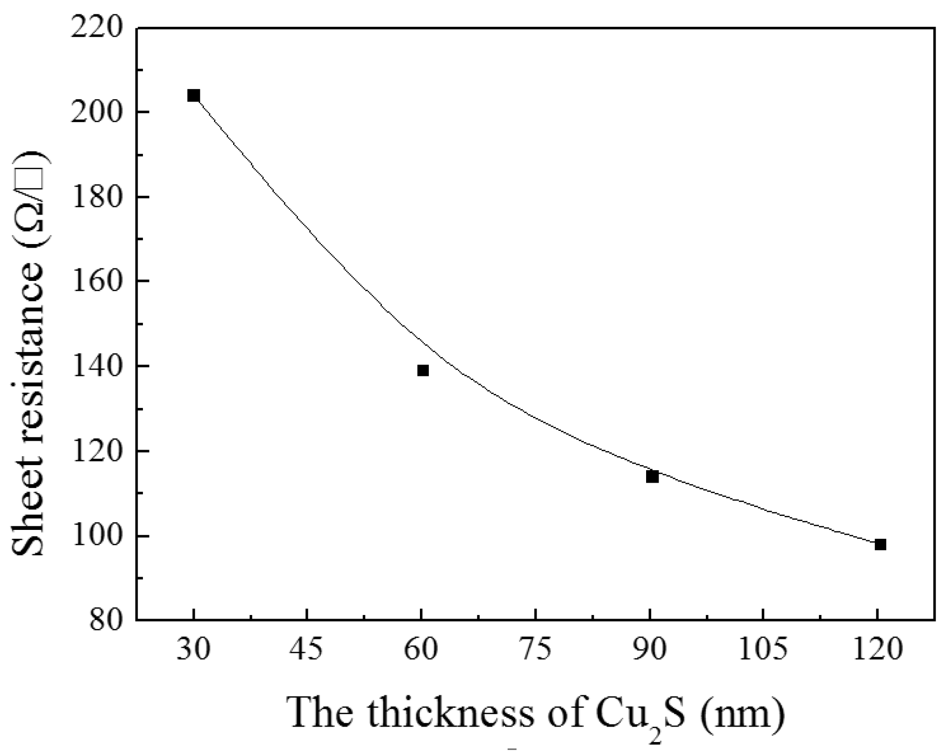
- For Cu2S/ZnO combination, the ZnO layer was deposited with a thickness around 60 nm, and then the Cu2S was deposited on the ZnO layer. The thickness of Cu2S varied from 0 nm to 120 nm.
- (2)
- For ZnO/Cu2S combination, the ZnO was deposited on the Cu2S layer whose thickness was 60 nm. The ZnO layer thickness varied from 0 nm to 60 nm.
- (3)
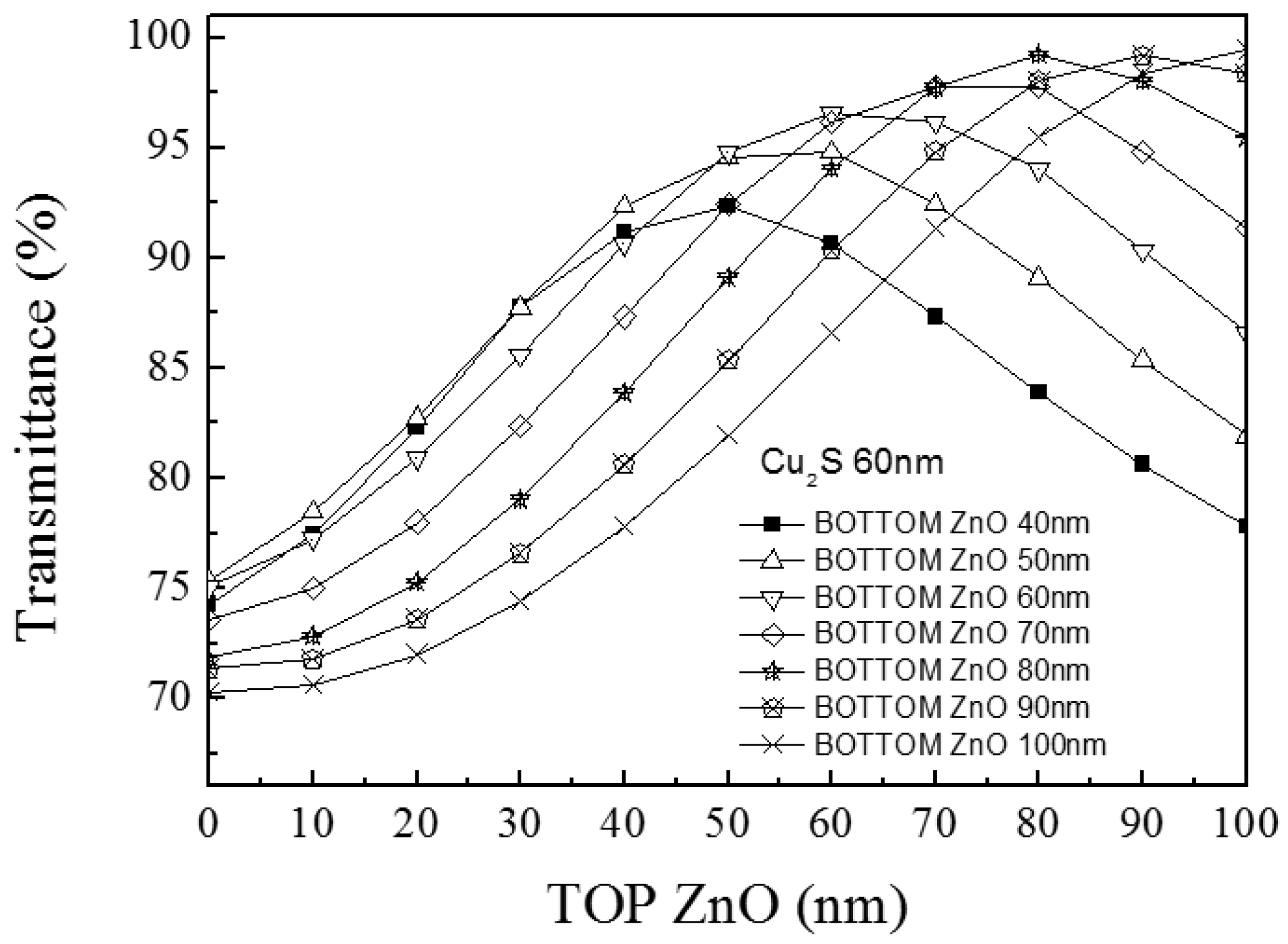
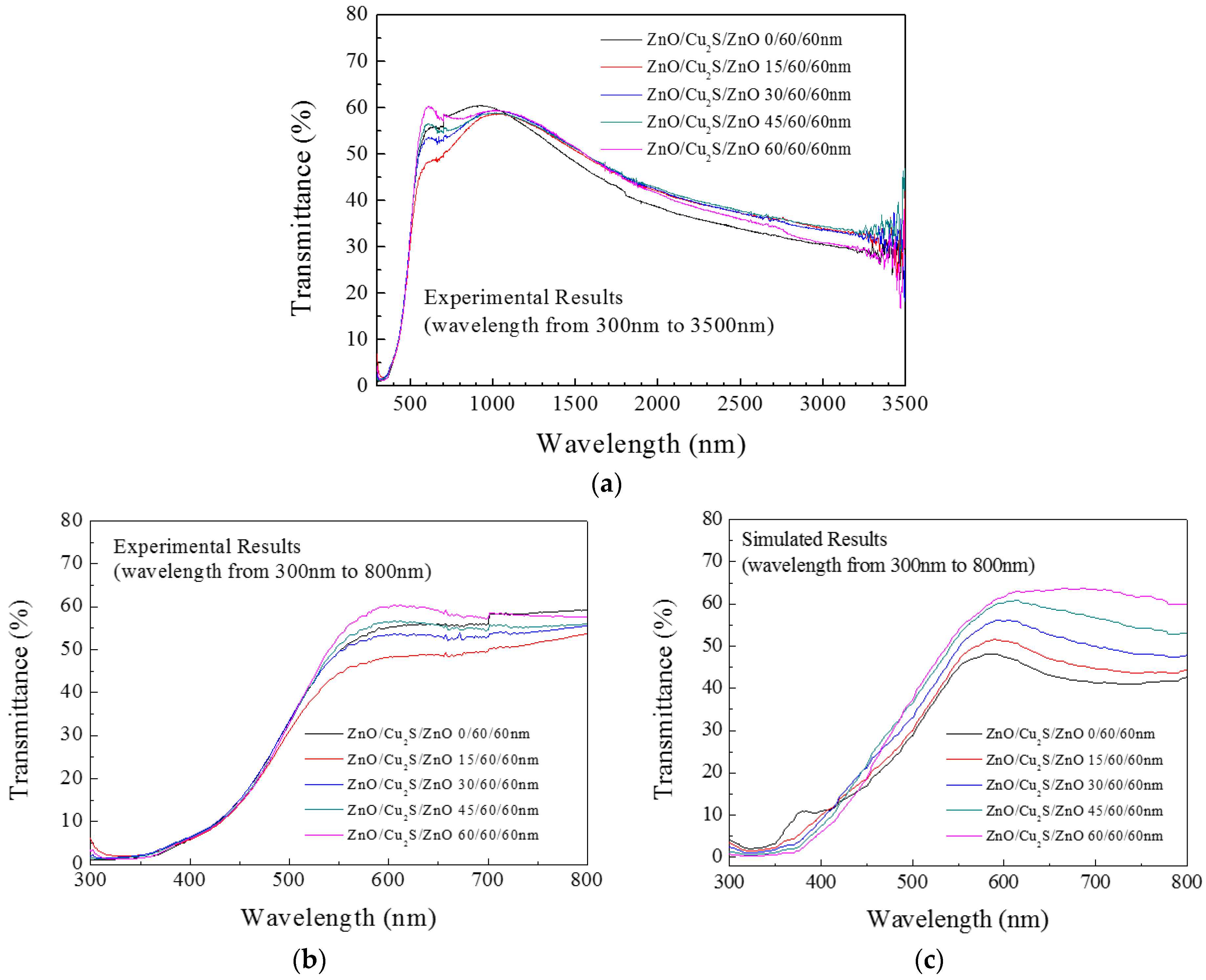
- For the ZnO/Cu2S/ZnO combination, bottom ZnO thickness was fixed at 60 nm, and the Cu2S layer thickness was fixed at 60 nm. The top ZnO layer varied from 0 nm to 60 nm.
3. Results and Discussion
3.1. Monolithic Film
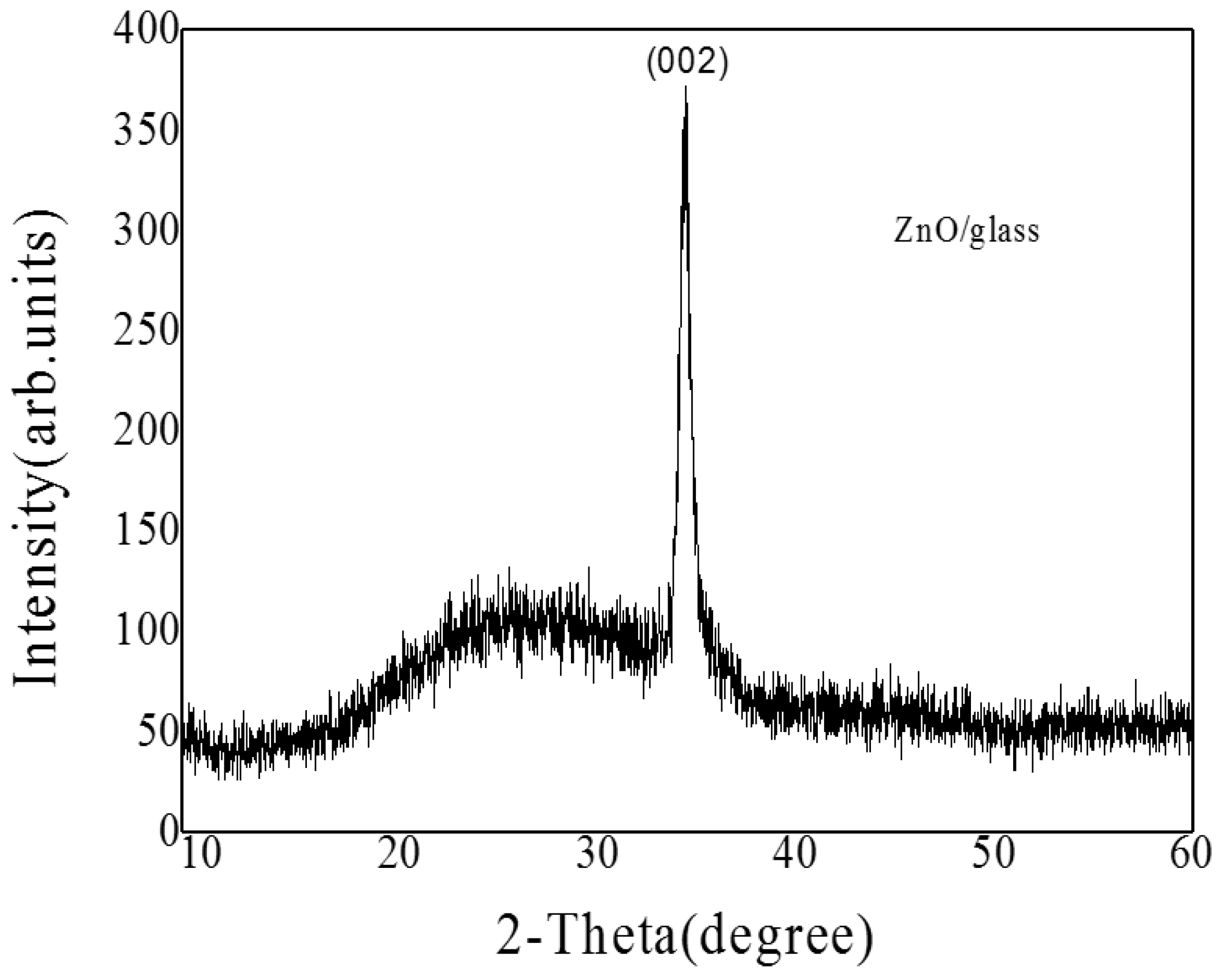
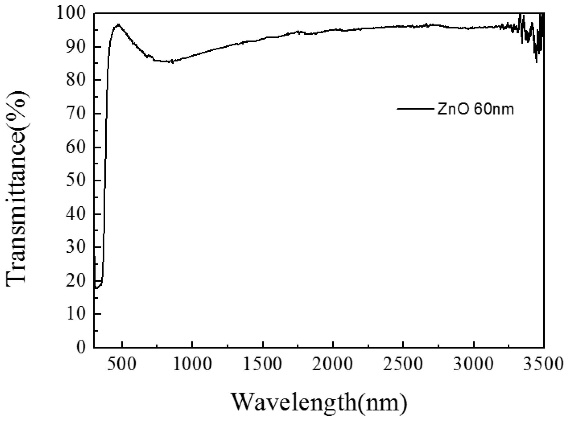
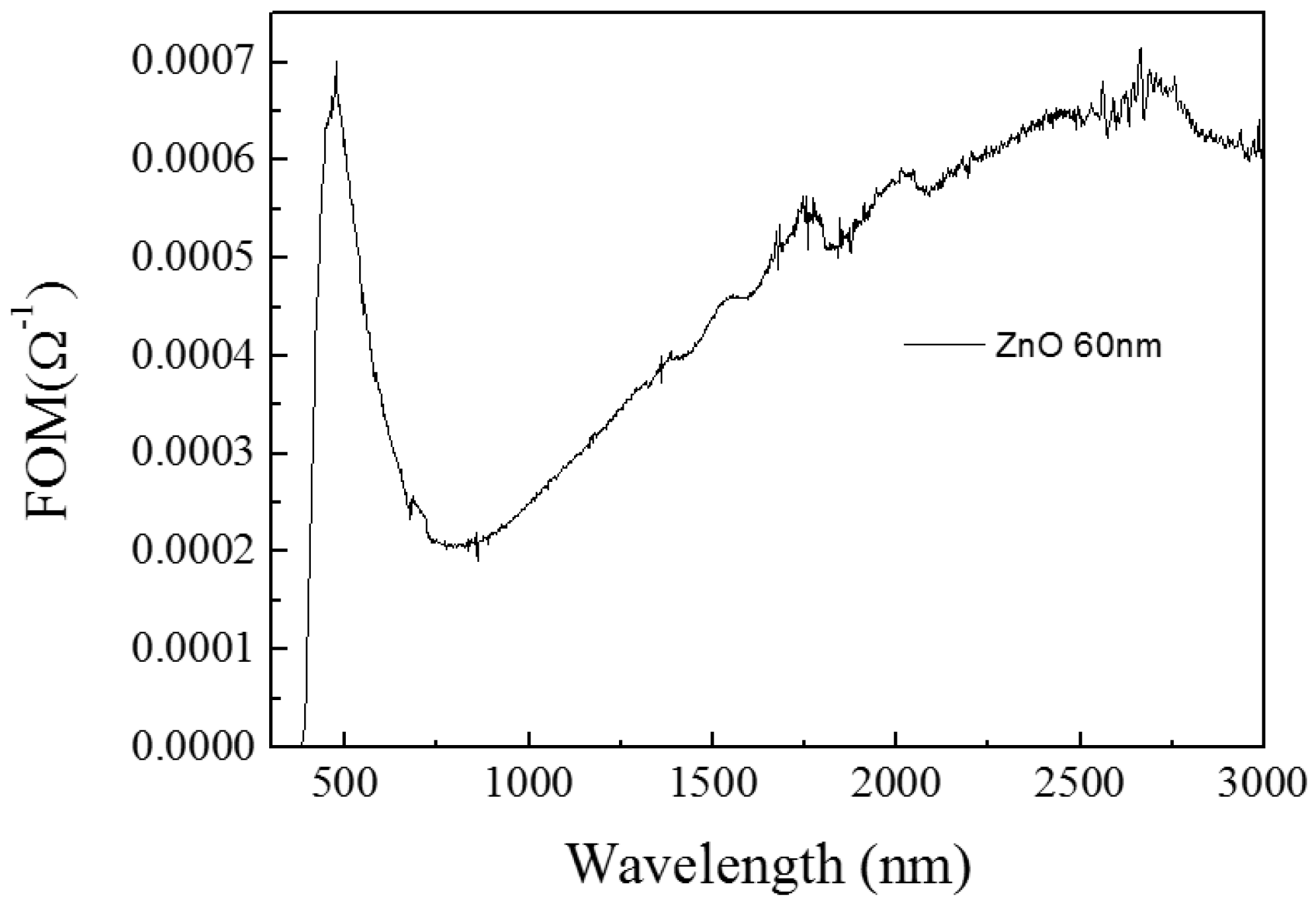
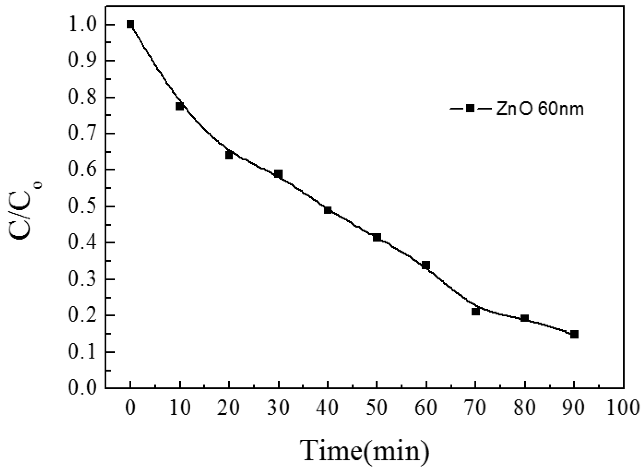
3.1.1. ZnO/Glass
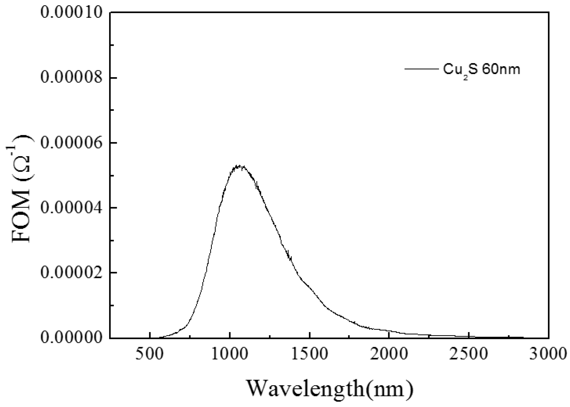
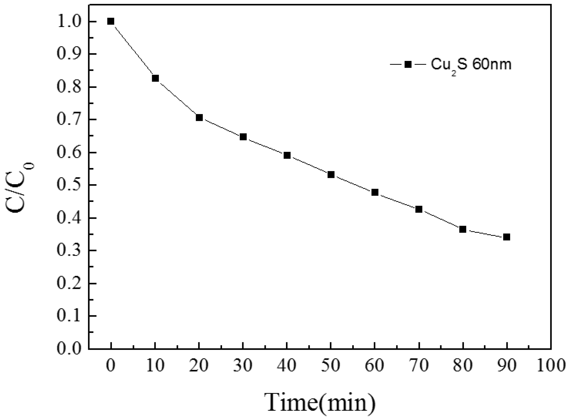
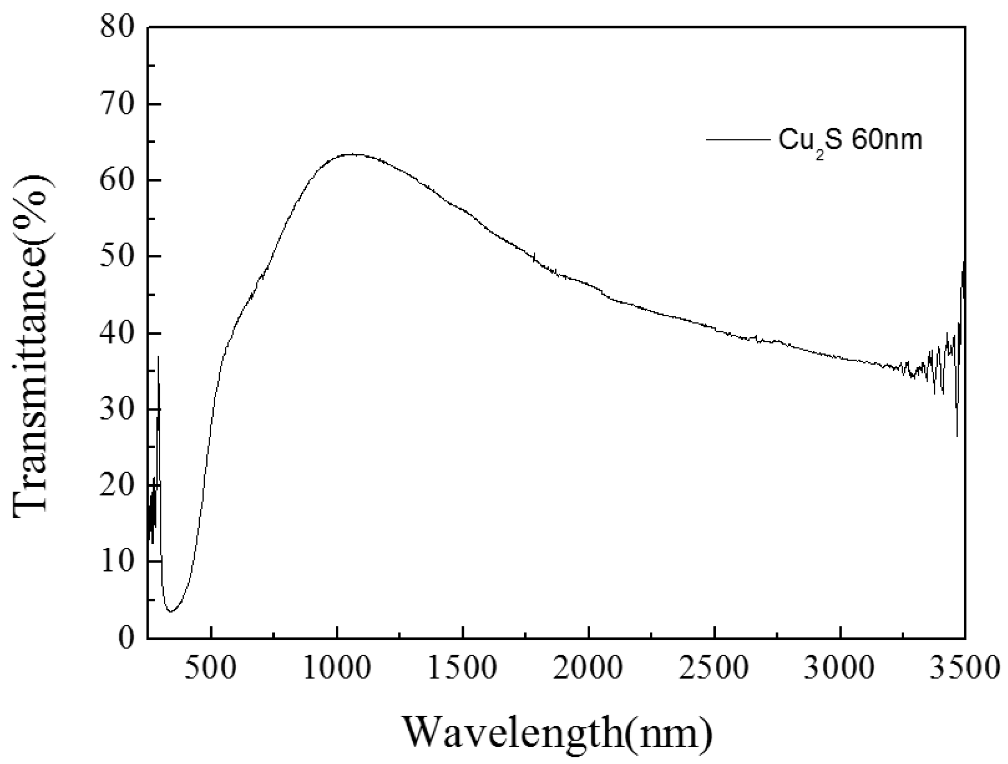
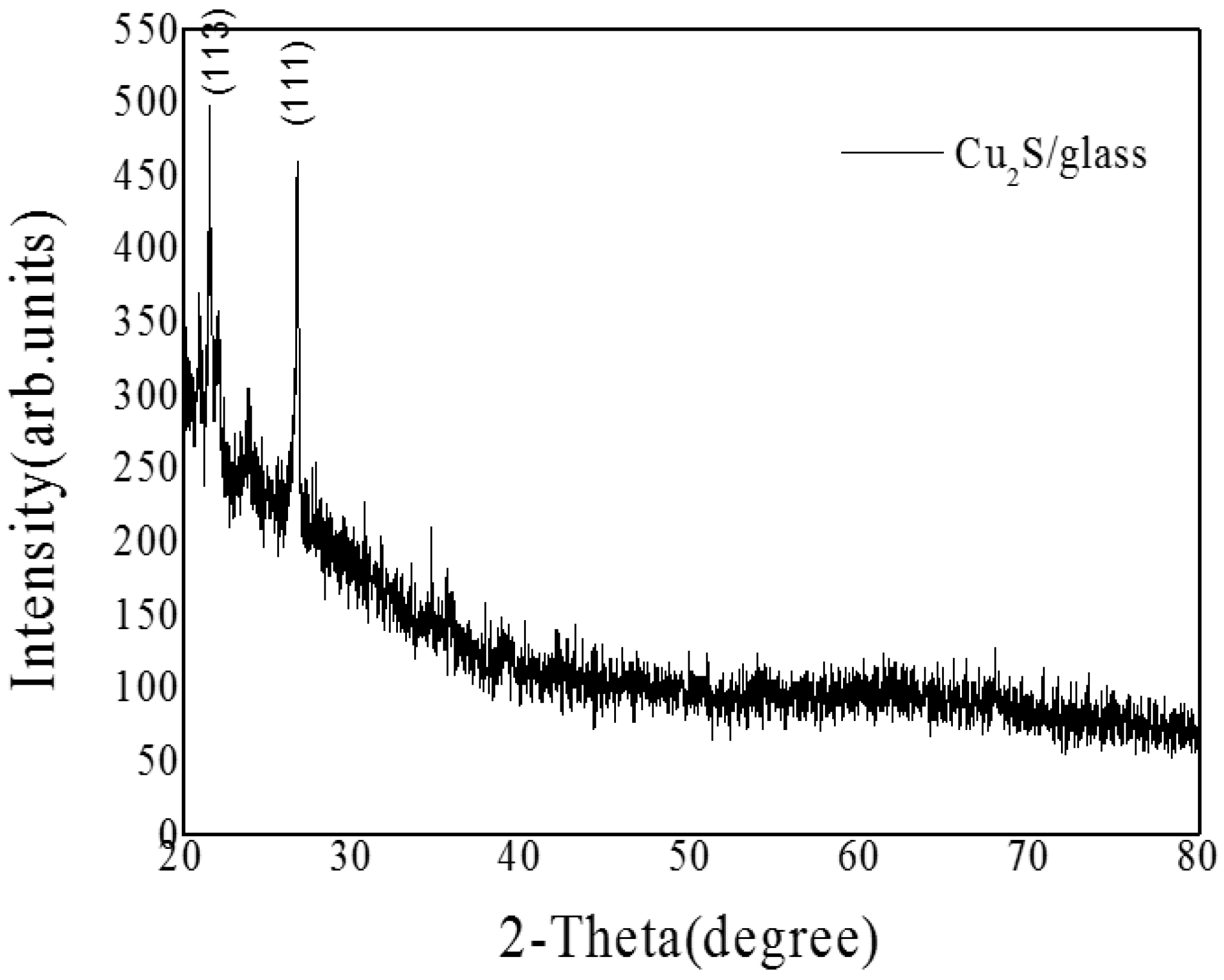
3.1.2. Cu2S/Glass
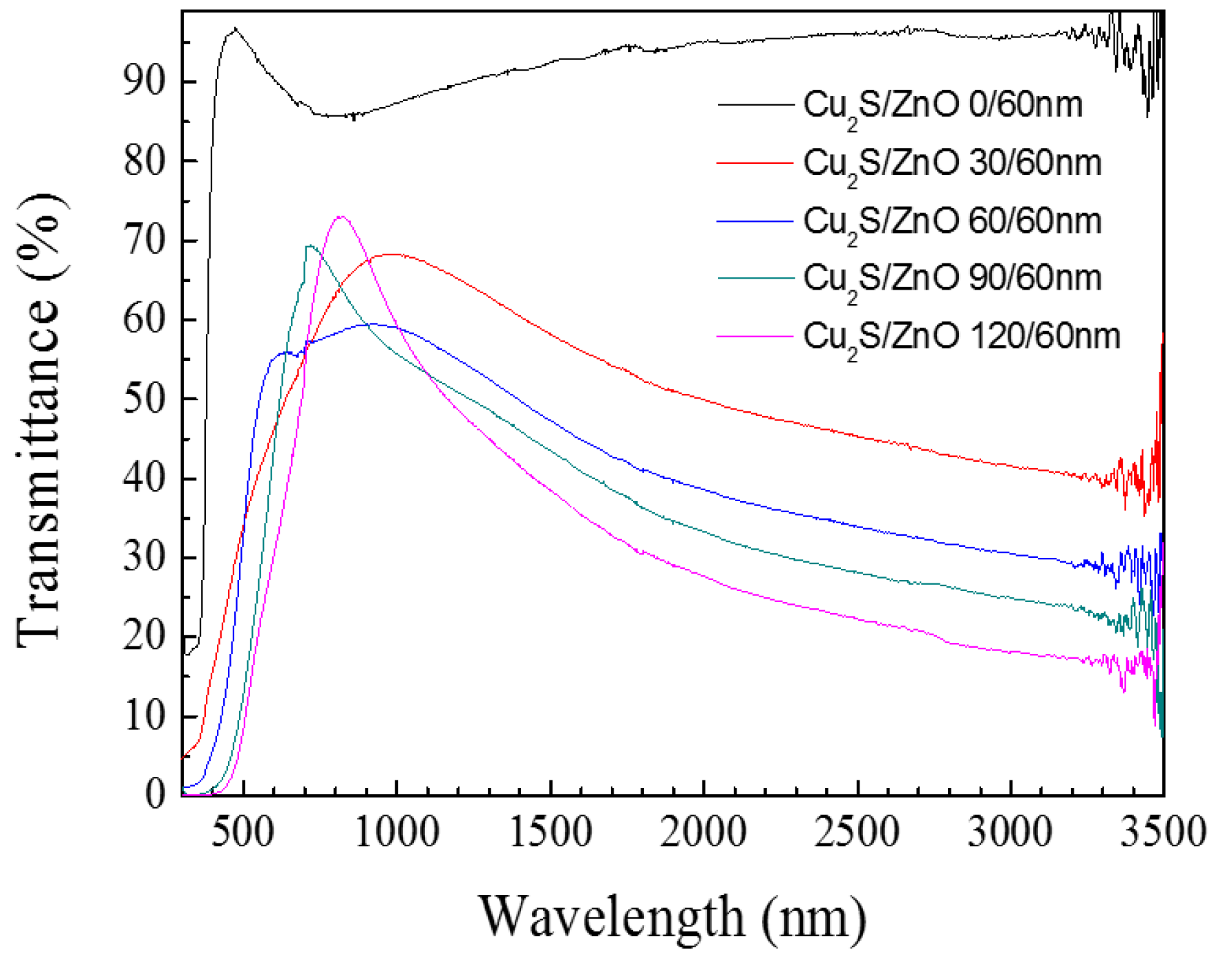
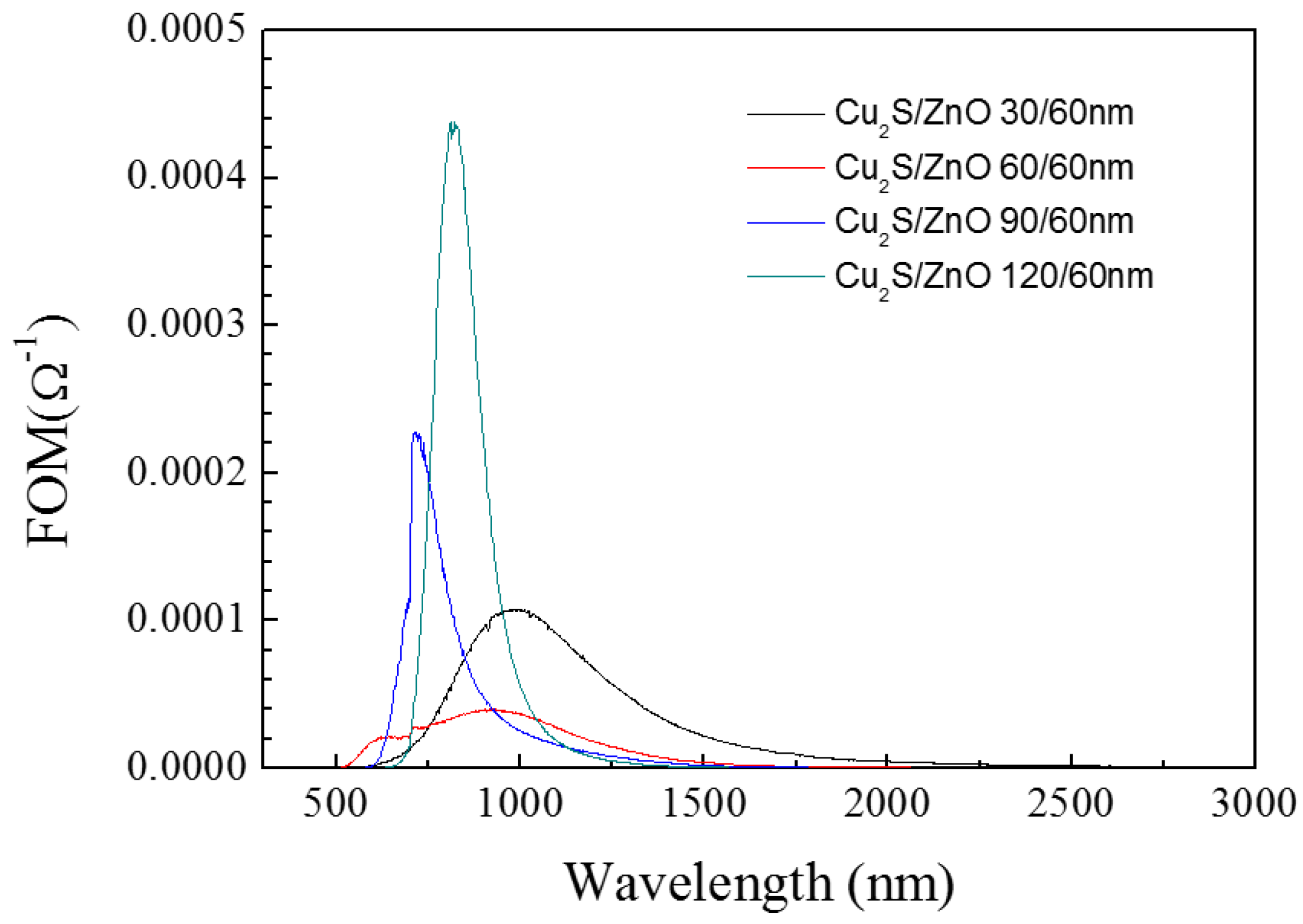
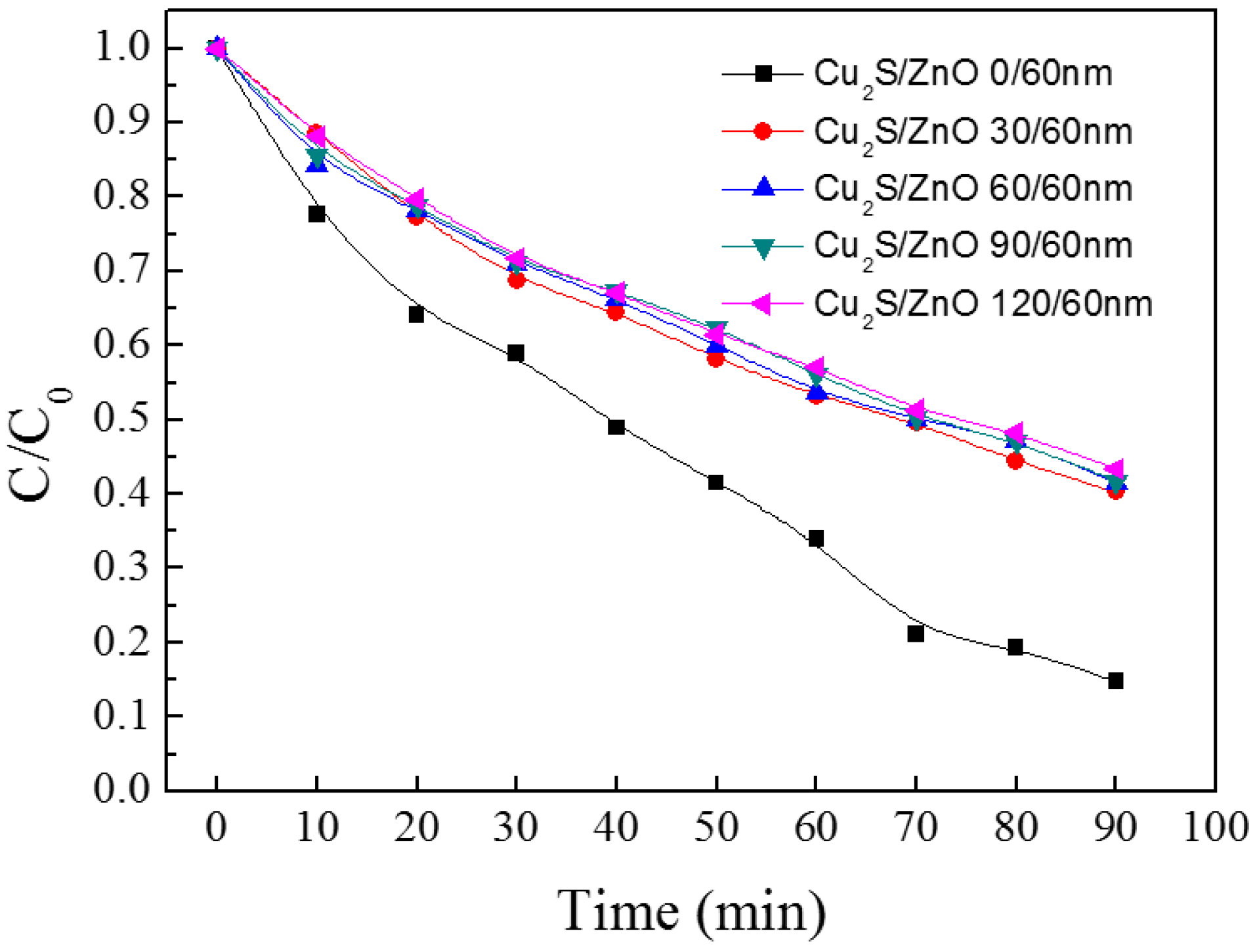
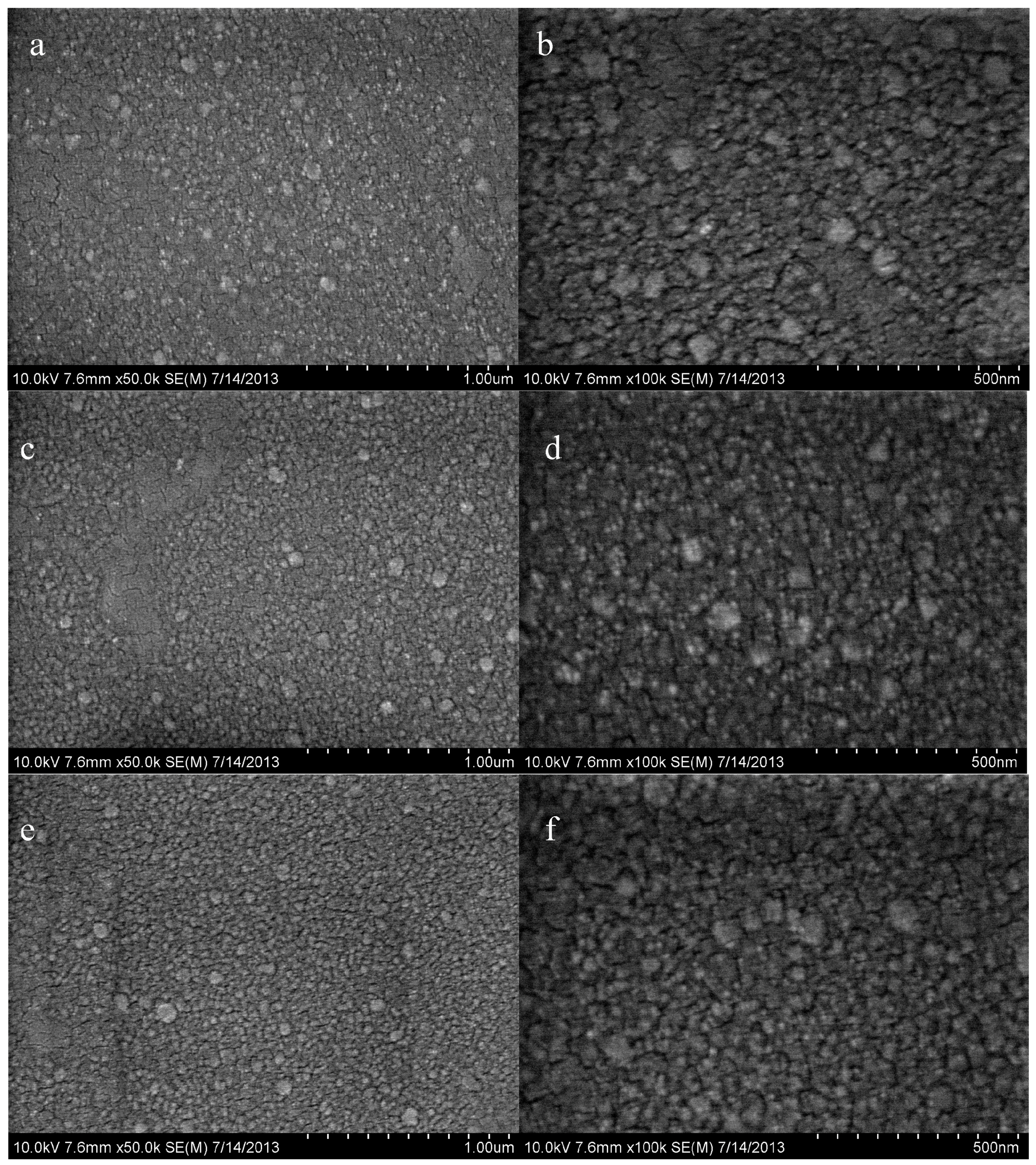
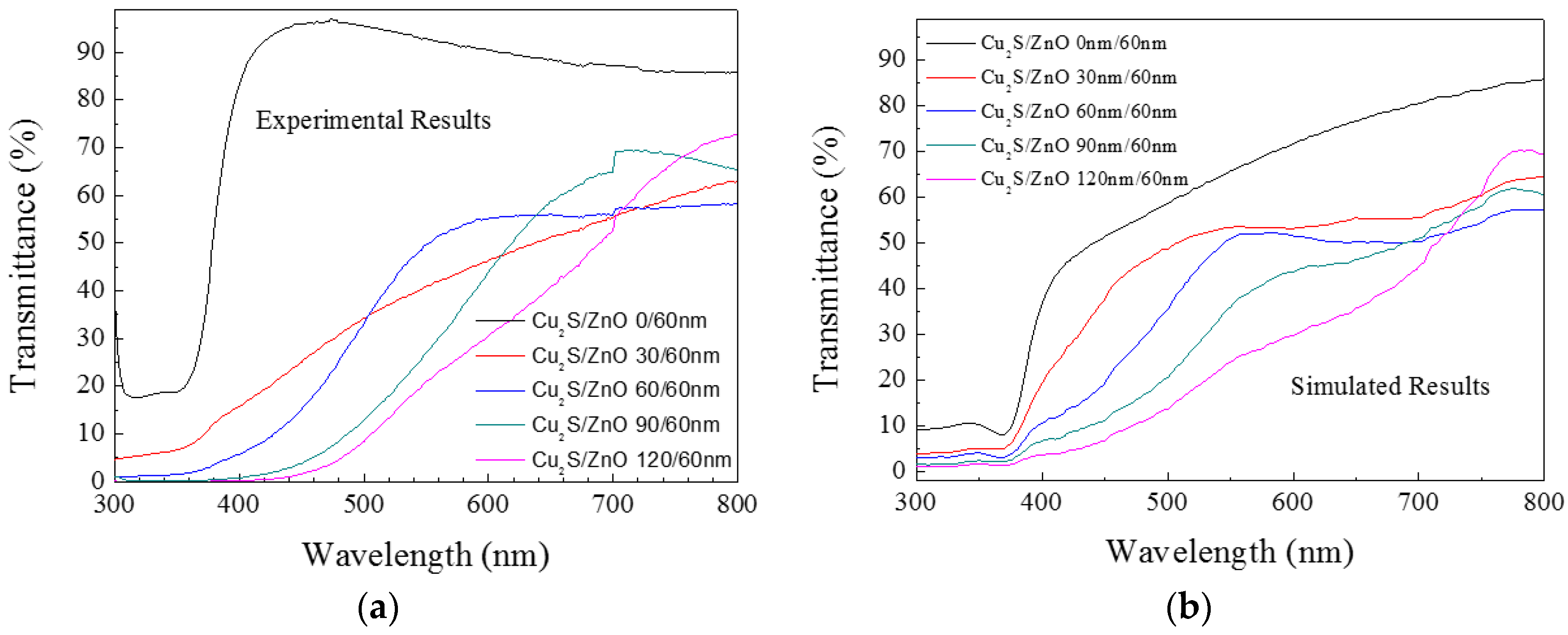
3.2. Cu2S/ZnO/Glass
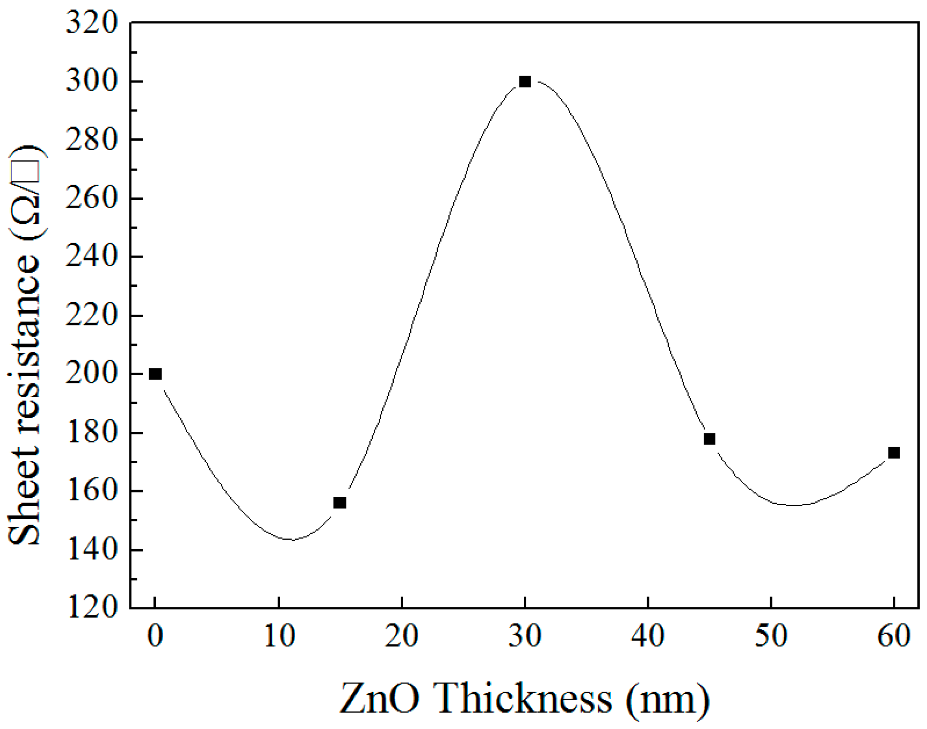
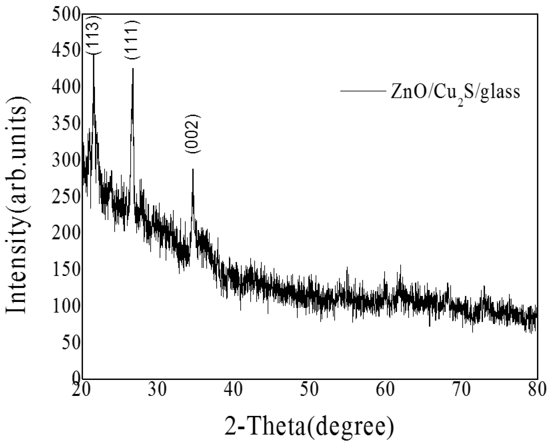
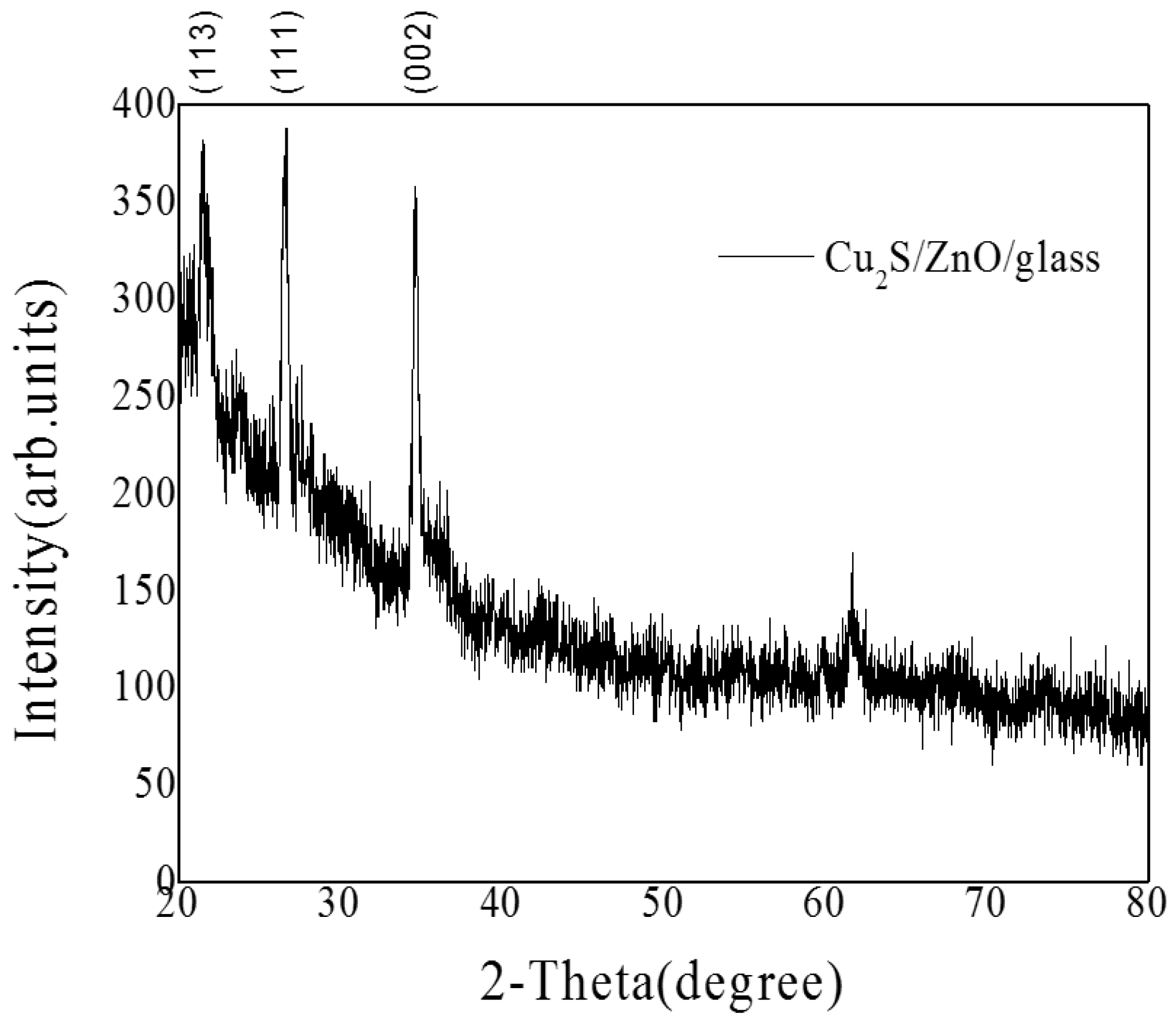
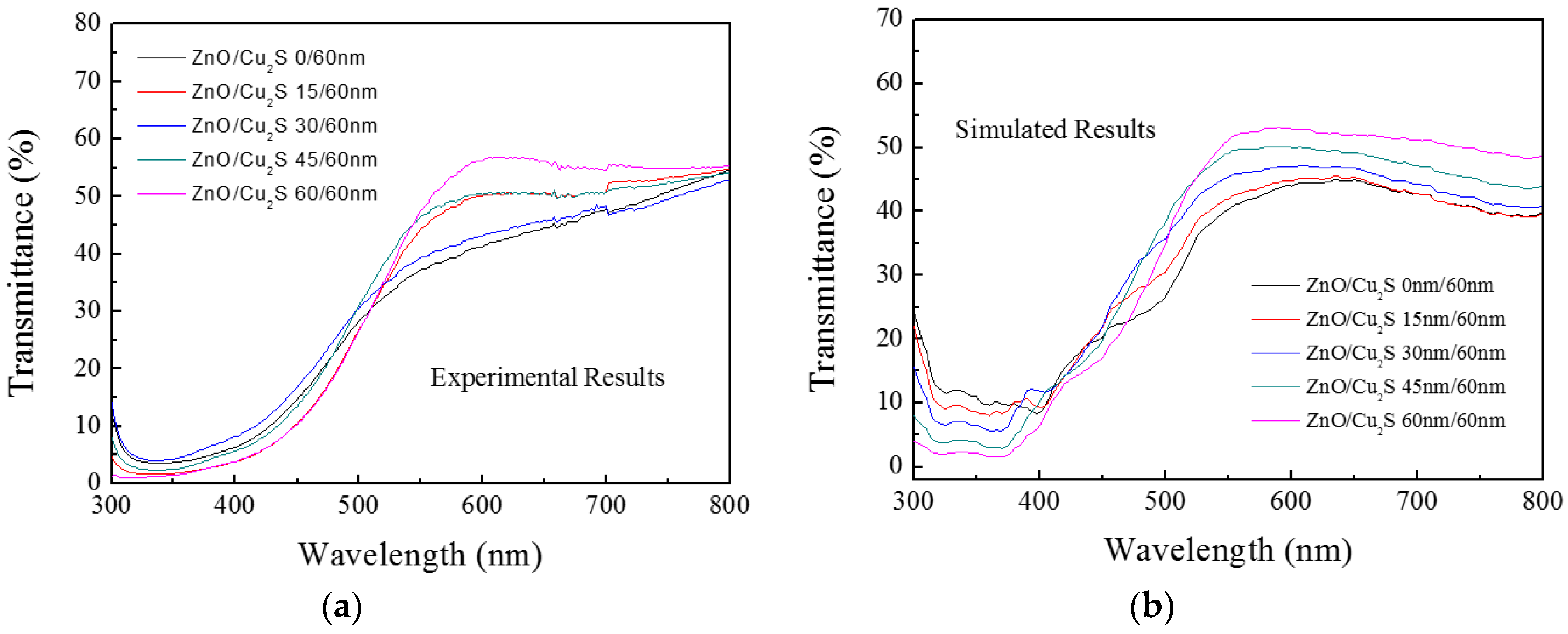
3.3. ZnO/Cu2S/Glass
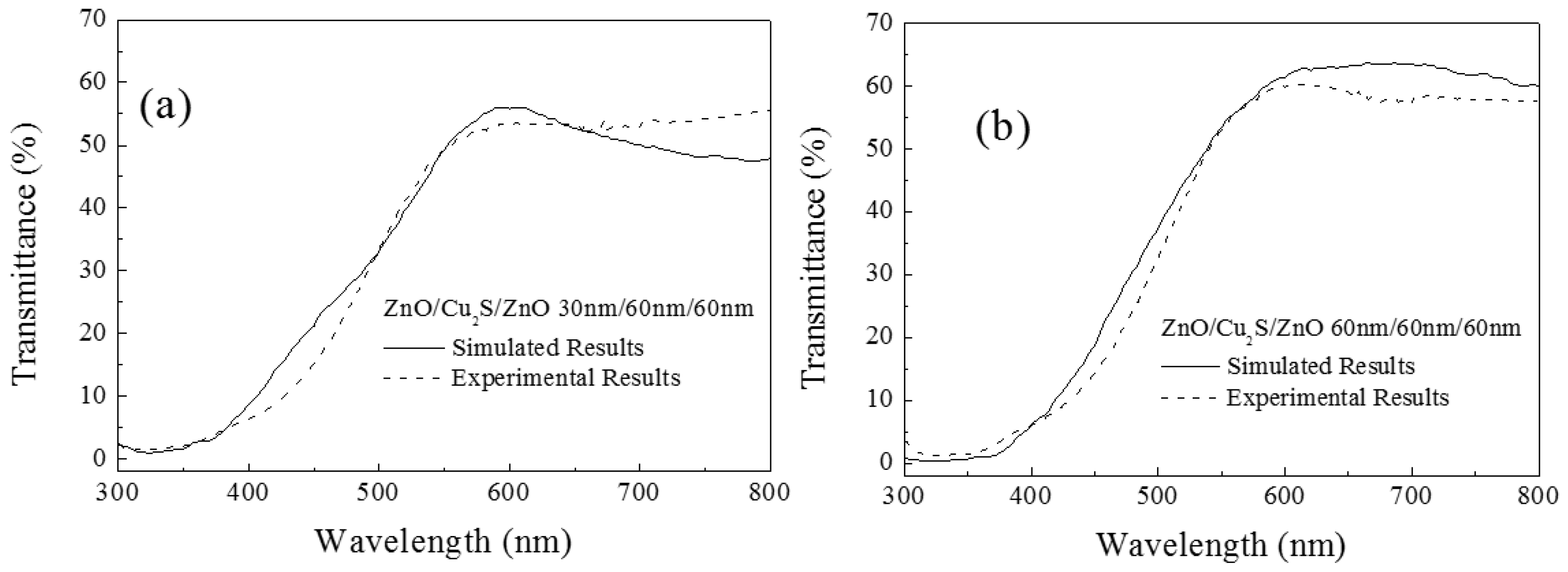
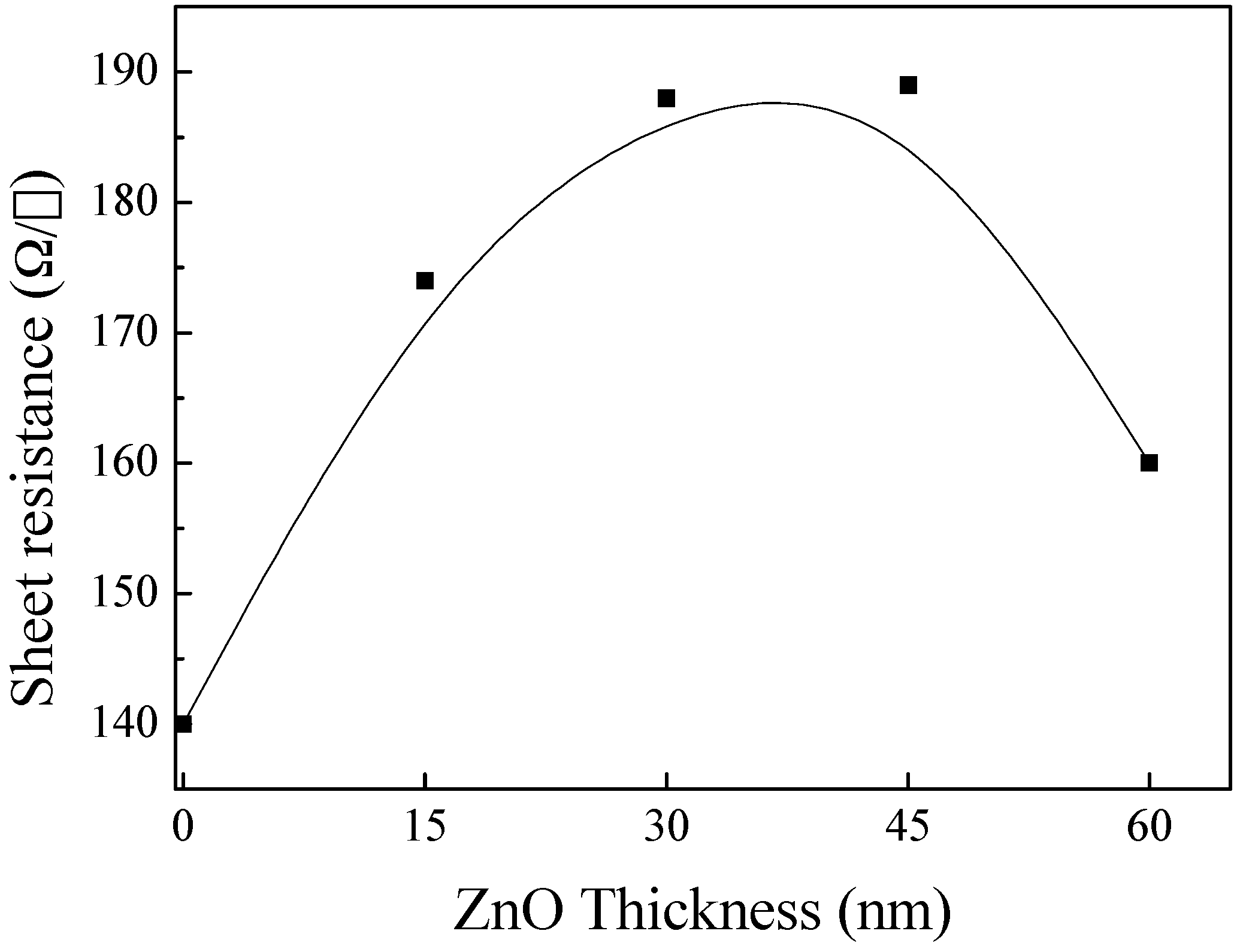
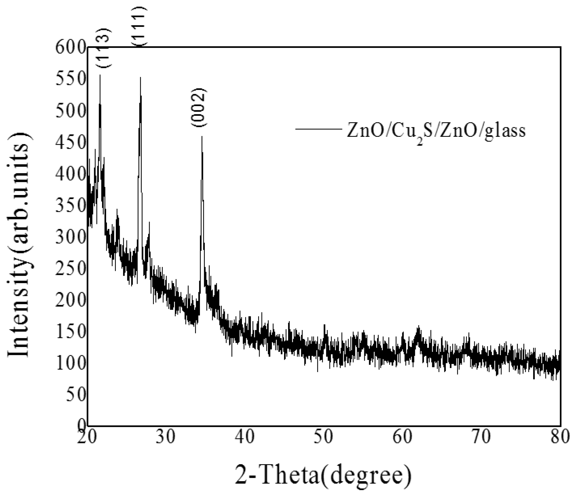
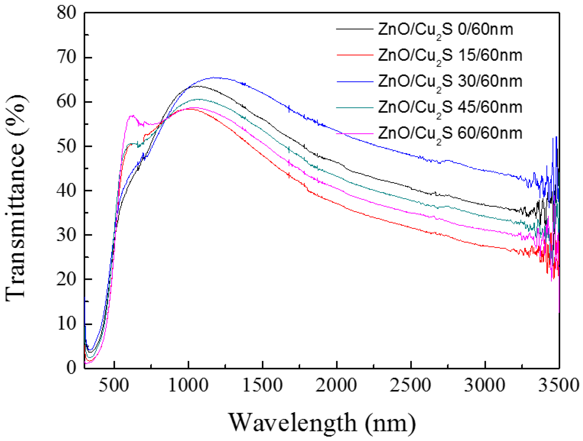
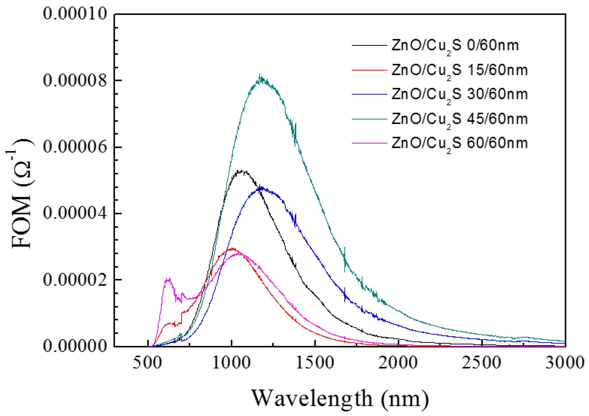
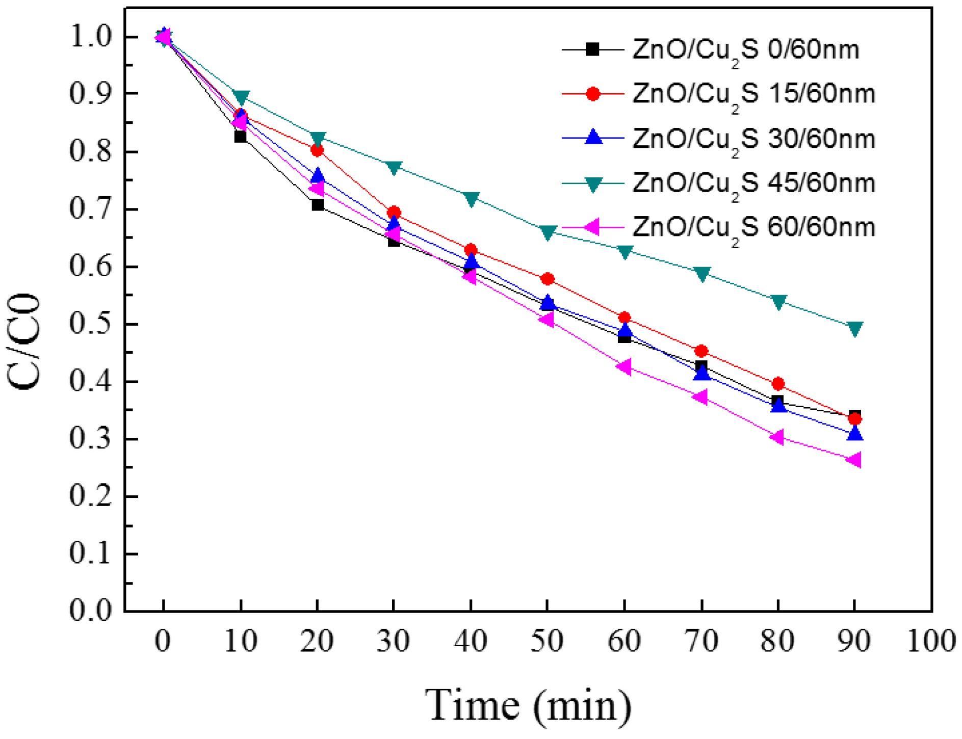
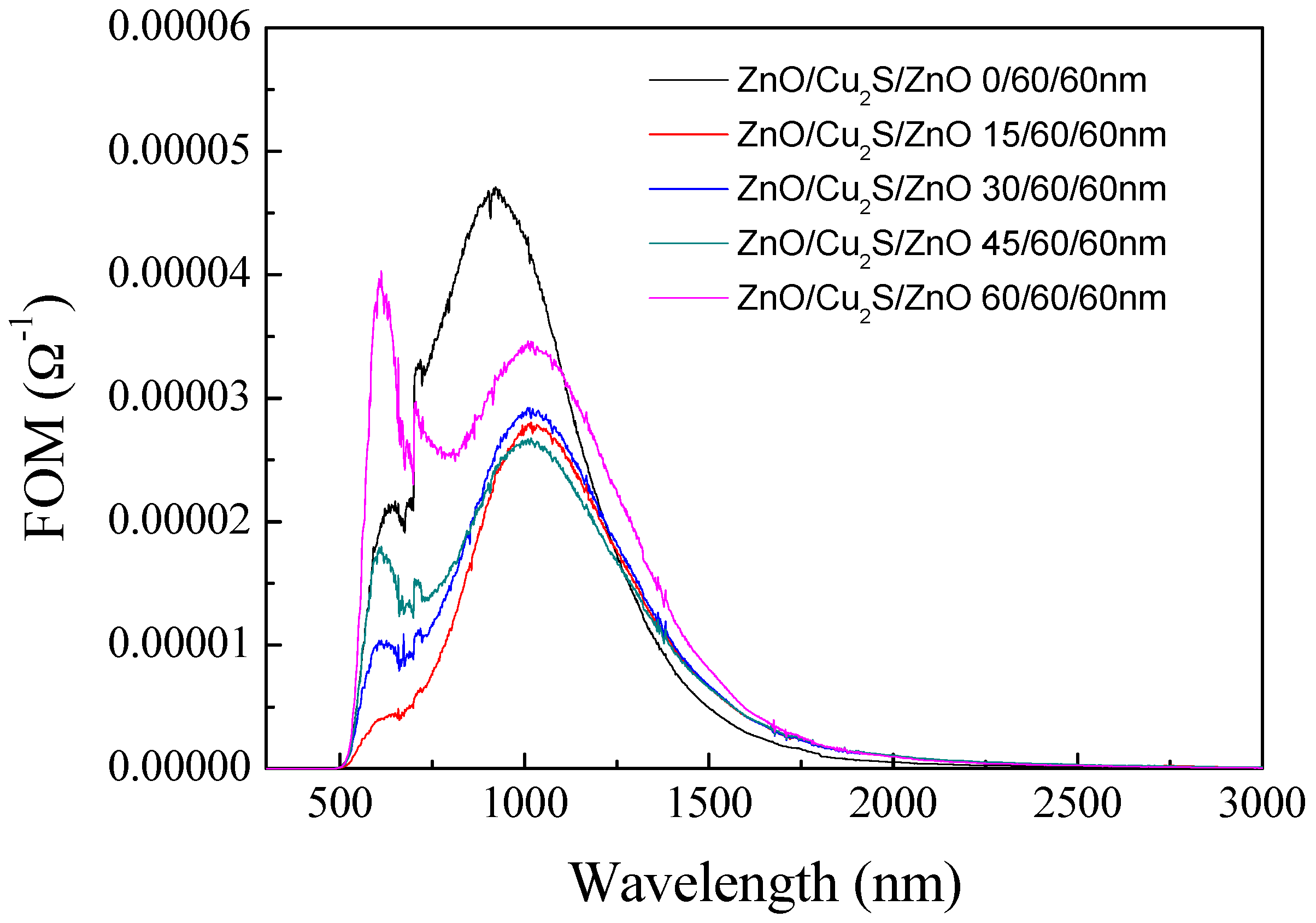
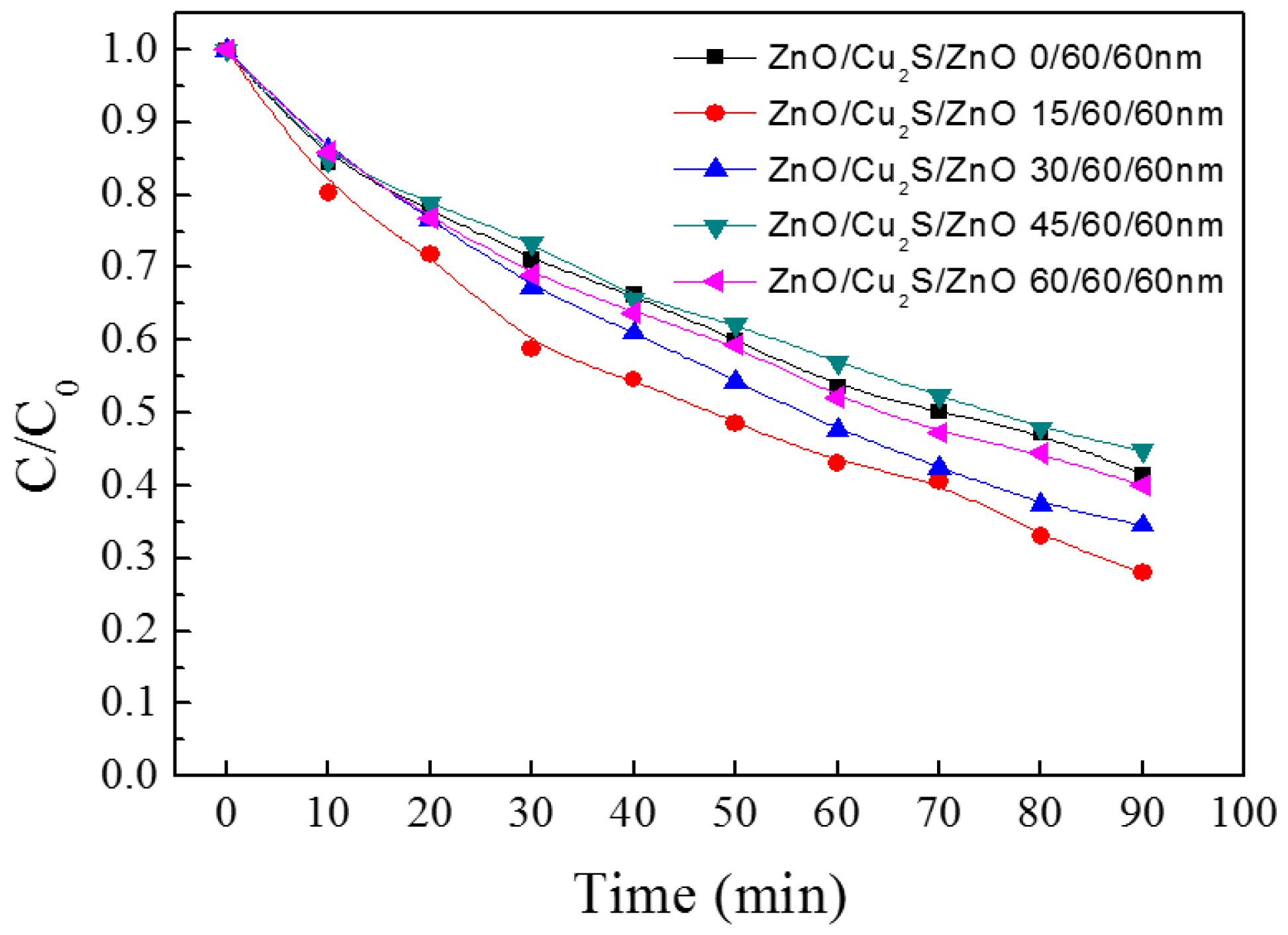
3.4. ZnO/Cu2S/ZnO/Glass
4. Conclusions
Acknowledgments
Author Contributions
Conflicts of Interest
References
- Kundu, S.; Sain, S.; Satpati, B.; Bhattacharyya, S.R.; Pradhan, S.K. Structural interpretation, growth mechanism and optical properties of ZnO nanorods synthesized by a simple wet chemical route. RSC Adv. 2015, 5, 23101–23113. [Google Scholar] [CrossRef]
- Ren, S.; Wang, B.; Zhang, H.; Ding, P.; Wang, Q. Sandwiched ZnO@Au@Cu2O Nanorod Films as Efficient Visible-Light-Driven Plasmonic Photocatalysts. ACS Appl. Mater. Interfaces 2015, 7, 4066–4074. [Google Scholar] [CrossRef] [PubMed]
- Chen, P.; Gu, L.; Cao, X.B. From single ZnO multipods to heterostructured ZnO/ZnS, ZnO/ZnSe, ZnO/Bi2S3 and ZnO/Cu2S multipods: Controlled synthesis and tunable optical and photoelectronchemical properties. Cryst. Eng. Commun. 2010, 12, 3950–3958. [Google Scholar] [CrossRef]
- Wu, Y.; Tamaki, T.; Volotinen, T.; Belova, L.; Rao, K.V. Enhanced photoresponse of inkjet-printed ZnO thin films capped with CdS nanoparticles. J. Phys. Chem. Lett. 2010, 1, 89–92. [Google Scholar] [CrossRef]
- Li, B.X.; Wang, Y.F. Facile synthesis and photocatalytic activity of ZnO-CuO nanocomposite. Superlattices Microstruct. 2010, 47, 615–623. [Google Scholar] [CrossRef]
- Wei, S.Q.; Chen, Y.Y.; Ma, Y.Y.; Shao, Z.C. Fabrication of CuO/ZnO composite films with cathodic co-electrodeposition and their photocatalytic performance. J. Mol. Catal. A 2010, 331, 112–116. [Google Scholar] [CrossRef]
- Wang, J.; Fan, X.M.; Wu, D.Z.; Dai, J.; Liu, H.; Liu, H.R.; Zhou, Z.W. Fabrication of CuO/T-ZnOw nanocomposites using photo-deposition and their photocatalytic property. Appl. Surf. Sci. 2011, 258, 1797–1805. [Google Scholar] [CrossRef]
- Zheng, L.R.; Zheng, Y.H.; Chen, C.Q.; Zhan, Y.Y.; Lin, X.Y.; Zheng, Q.; Wei, K.M.; Zhu, J.F. Network structured SnO2/ZnO heterojunction nanocatalyst with high photo catalytic activity. Inorg. Chem. 2009, 48, 1819–1825. [Google Scholar] [CrossRef] [PubMed]
- Chen, T.W.; Zheng, Y.H.; Lin, J.M.; Chen, G.N. Study on the photocatalytic degradation of methyl orange in water using Ag/ZnO as catalyst by liquid chromatography electronspray ionizationion-trap mass spectrometry. J. Am. Soc. Mass Spectrom. 2008, 19, 997–1003. [Google Scholar] [CrossRef] [PubMed]
- Dhar, A.; Alford, T.L. High quality transparent TiO2/Ag/TiO2 composite electrode films deposited on flexible substrate at room temperature by sputtering. APL Mater. 2013, 1. [Google Scholar] [CrossRef]
- Liu, X.Y.; Li, Y.A.; Liu, S.; Wu, H.L.; Cui, H.N. ZnO/Cu/ZnO multilayer films: Structure optimization and investigation on photoelectric properties. Thin Solid Films 2012, 520, 5372–5377. [Google Scholar] [CrossRef]
- Sahu, D.R.; Lin, S.Y.; Huang, J.L. ZnO/Ag/ZnO multilayer films for the application of a very low resistance transparent electrode. Appl. Surf. Sci. 2006, 252, 7509–7514. [Google Scholar] [CrossRef]
- Sahu, D.R.; Huang, J.L. High quality transparent conductive ZnO/Ag/ZnO multilayer films deposited at room temperature. Thin Solid Films 2006, 515, 876–879. [Google Scholar] [CrossRef]
- Siol, S.; Hellmann, J.C.; Tilley, S.D.; Graetzel, M.; Morasch, J.; Deuermeier, J.; Jaegermann, W.; Klein, A. Band Alignment Engineering at Cu2O/ZnO Heterointerfaces. ACS Appl. Mater. Interfaces 2016, 8, 21824–21831. [Google Scholar] [CrossRef] [PubMed]
- Jiang, X.; Lin, Q.; Zhang, M.; He, G.; Sun, Z. Microstructure, optical properties, and catalytic performance of Cu2O-modified ZnO nanorods prepared by electrodeposition. Nanoscale Res. Lett. 2015, 10. [Google Scholar] [CrossRef] [PubMed]
- Wang, S.; Yang, S. Growth of crystalline Cu2S nanowire arrays onn copper surface: Effect of copper surface structure, reagent gas composition, and reaction temperature. Chem. Mater. 2001, 13, 4794–4799. [Google Scholar] [CrossRef]
- Liao, X.H.; Chen, N.Y.; Xu, S.; Yang, S.B.; Zhu, J.J. A microwave assisted heating method for the preparation of copper sulfidenanorods. Cryst. Growth 2003, 252, 593–598. [Google Scholar] [CrossRef]
- Xu, F.; Volkov, V.; Zhu, Y.; Bai, H.; Rea, A.; Valappil, N.V.; Su, W.; Gao, X.; Kuskovsky, I.L.; Matsui, H. Long electron-holeseparation of ZnO–CdS core-shell quantum dots. J. Phys. Chem. C 2009, 113, 19419–19423. [Google Scholar] [CrossRef]
- Wu, D.Z.; Fan, X.M.; Dai, J.; Liu, H.R.; Liu, H.; Zhang, F. Preparation and Photocatalytic Properties of Cu2S/Tetrapod-Like ZnO Whisker Nanocomposites. Chin. J. Catal. 2012, 33, 802–807. [Google Scholar] [CrossRef]
- Zhang, J.; Yu, J.G.; Zhang, Y.M.; Li, Q.; Gong, J.R. Visible light photocatalytic H2-production activity of CuS/ZnS porous nanosheetsbased on photoinduced interfacial charge transfer. Nano Lett. 2011, 11, 4774–4779. [Google Scholar] [CrossRef] [PubMed]
- Haacke, G. New figure of merit for transparent conductors. Appl. Phys. 1976, 47, 4086–4089. [Google Scholar] [CrossRef]
- Born, M.; Wolf, E. Principles of Optics, 6th ed.; Pergamon: New York, NY, USA, 1980; p. 55. [Google Scholar]
- Liu, X.H.; Mayer, M.T.; Wang, D.W. Negative differential resistance and resistive switching behaviors in Cu2S nanowire devices. Appl. Phys. Lett. 2010, 96. [Google Scholar] [CrossRef]


© 2017 by the authors. Licensee MDPI, Basel, Switzerland. This article is an open access article distributed under the terms and conditions of the Creative Commons Attribution (CC-BY) license ( http://creativecommons.org/licenses/by/4.0/).
Share and Cite
Wang, Z.; Xu, F.; Wang, H.; Cui, H.-N.; Wang, H. ZnO/Cu2S/ZnO Multilayer Films: Structure Optimization and Its Detail Data for Applications on Photoelectric and Photocatalytic Properties. Materials 2017, 10, 37. https://doi.org/10.3390/ma10010037
Wang Z, Xu F, Wang H, Cui H-N, Wang H. ZnO/Cu2S/ZnO Multilayer Films: Structure Optimization and Its Detail Data for Applications on Photoelectric and Photocatalytic Properties. Materials. 2017; 10(1):37. https://doi.org/10.3390/ma10010037
Chicago/Turabian StyleWang, Zhenxing, Feng Xu, He Wang, Hai-Ning Cui, and Haishui Wang. 2017. "ZnO/Cu2S/ZnO Multilayer Films: Structure Optimization and Its Detail Data for Applications on Photoelectric and Photocatalytic Properties" Materials 10, no. 1: 37. https://doi.org/10.3390/ma10010037