
A Study of Dip-Coatable, High-Capacitance Ion Gel Dielectrics for 3D EWOD Device Fabrication


Abstract
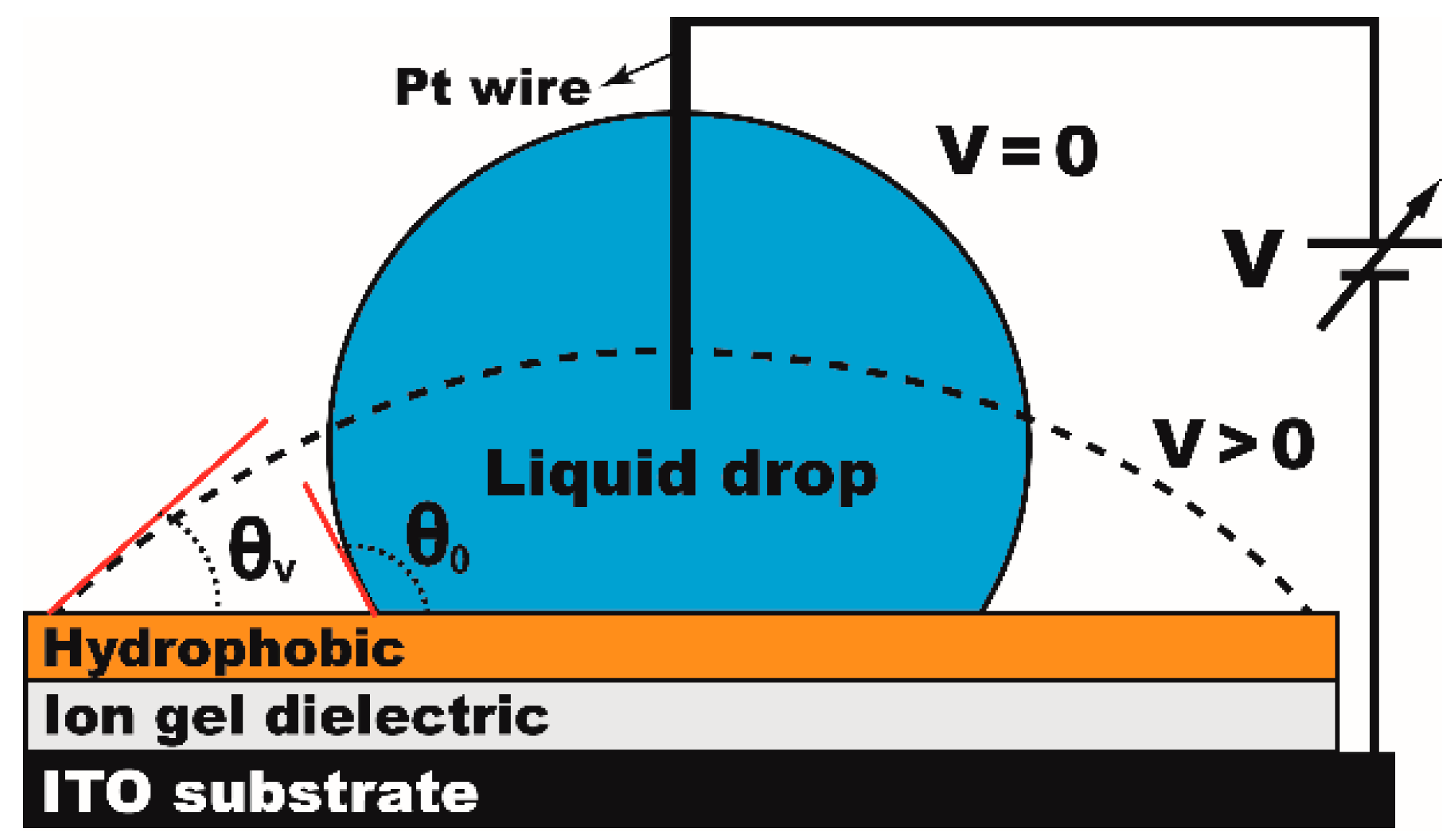
:1. Ion Gel Dielectrics for EWOD
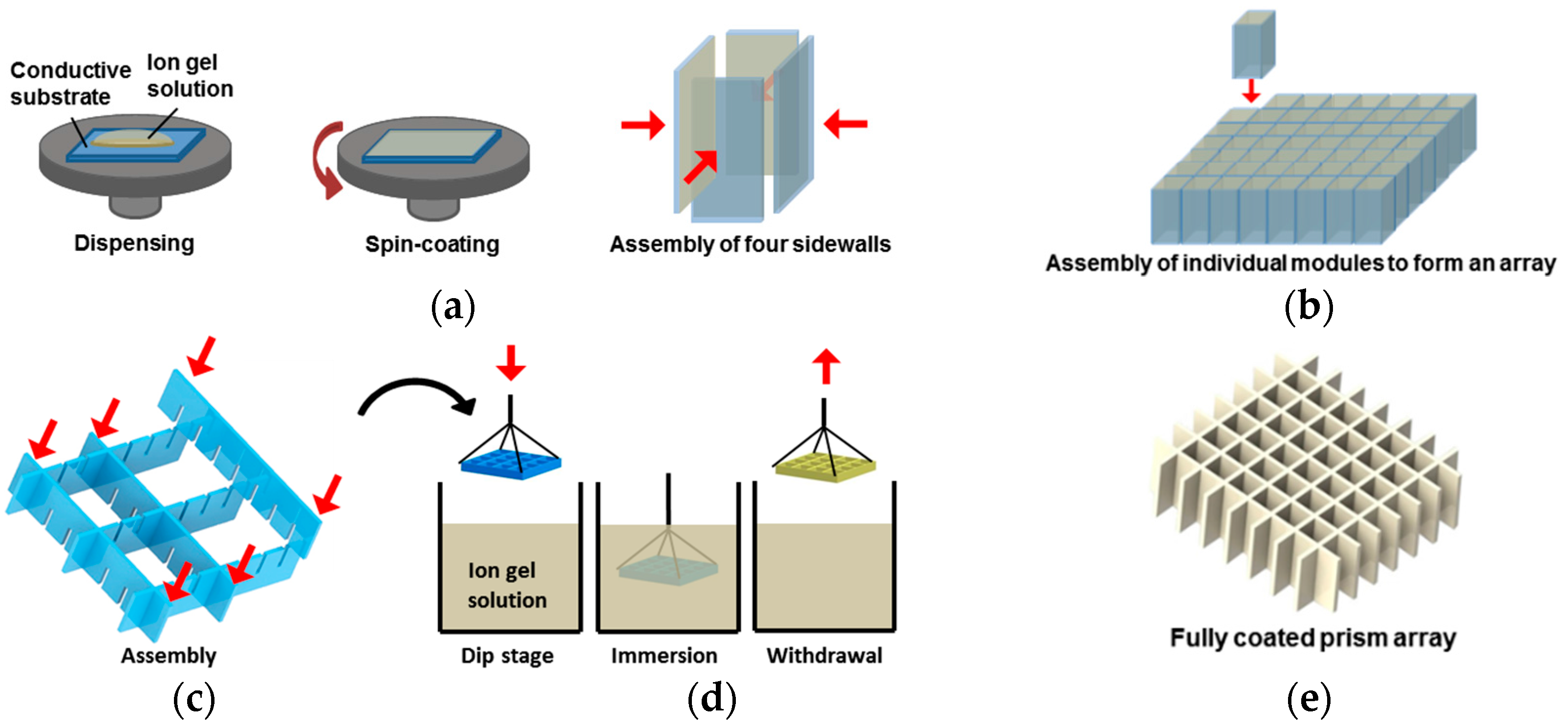
2. Ion Gel Layer Coating for 3D EWOD Device Fabrication
3. Materials and Methods
4. Experimental Results
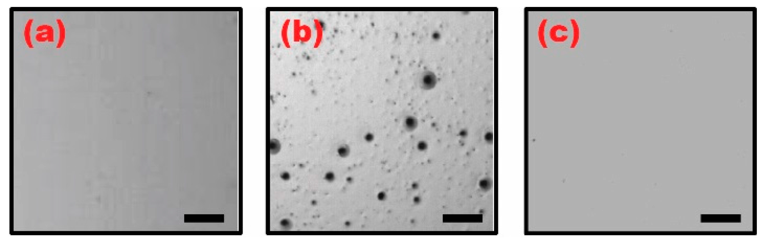
4.1. Manifestation of Surface Defects on the Ion Gel Layer Dip-Coated
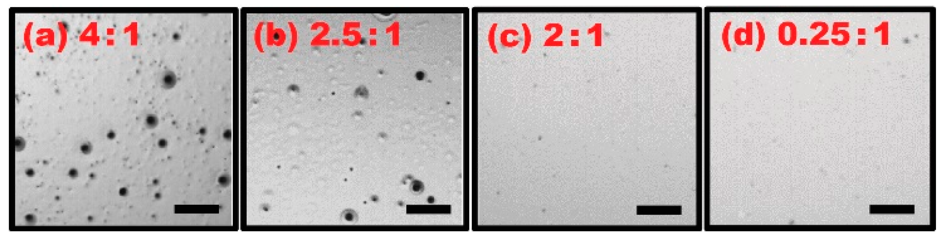
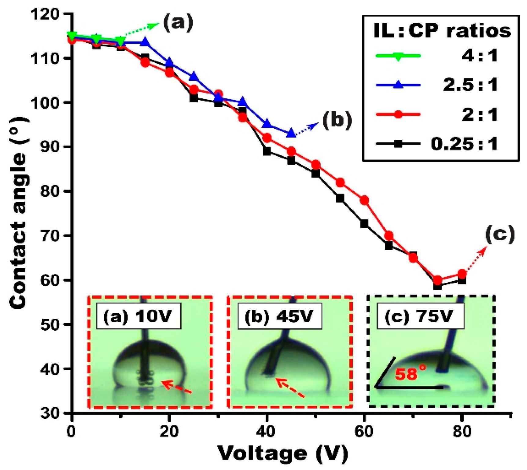
4.2. Effect of Ionic Liquid Concentrations on EWOD
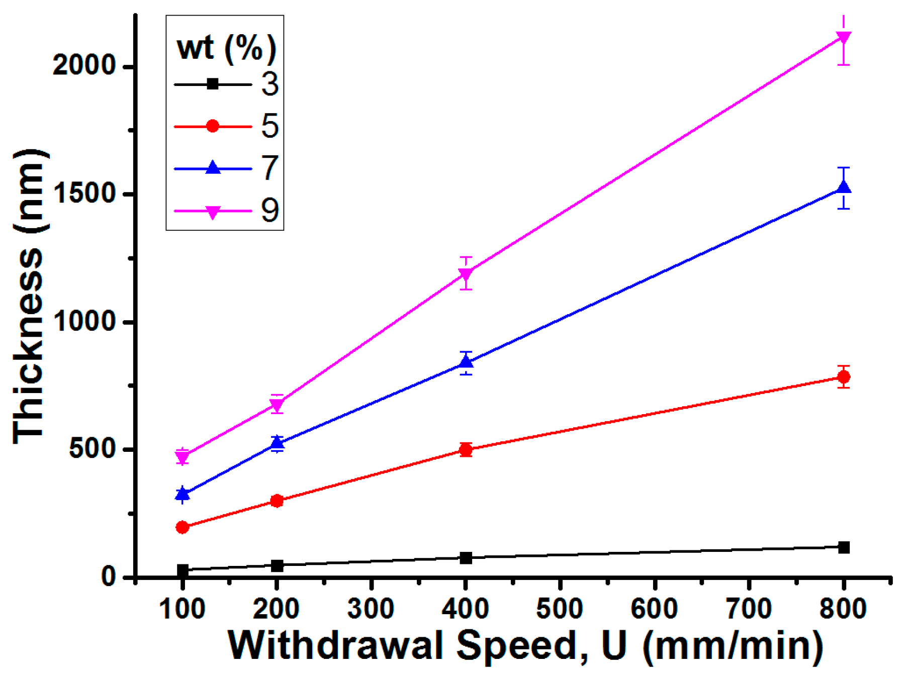
4.3. Thickness Control of the Dip-Coated Gel Layers
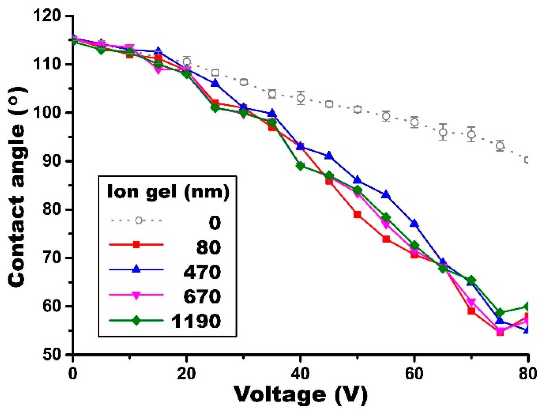
4.4. Thickness Effect of the Dip-Coated Gel Layers
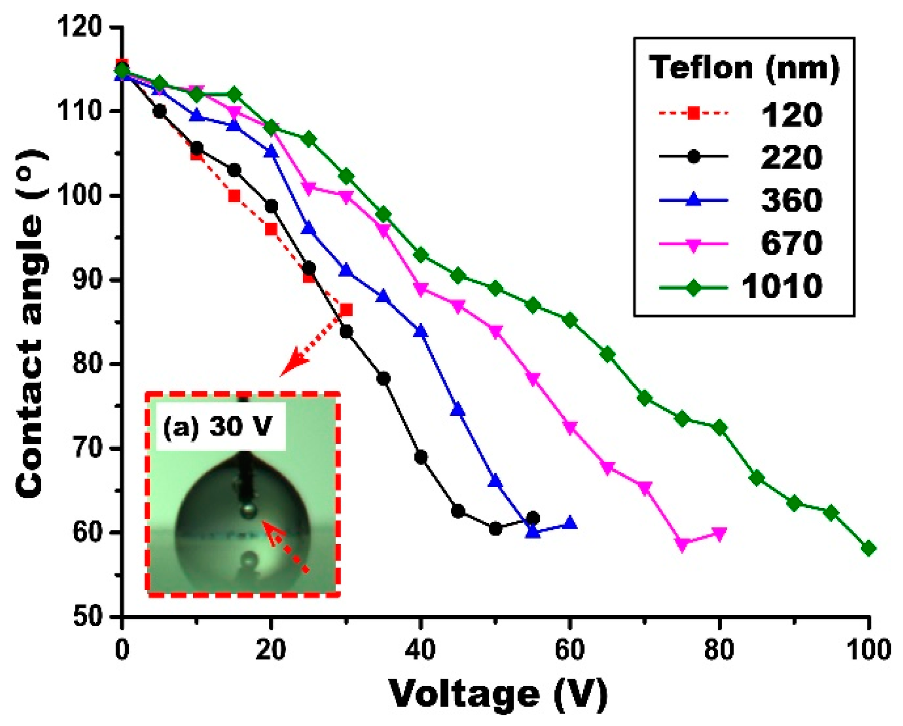
4.5. Thickness Effect of the Dip-Coated Teflon Layers
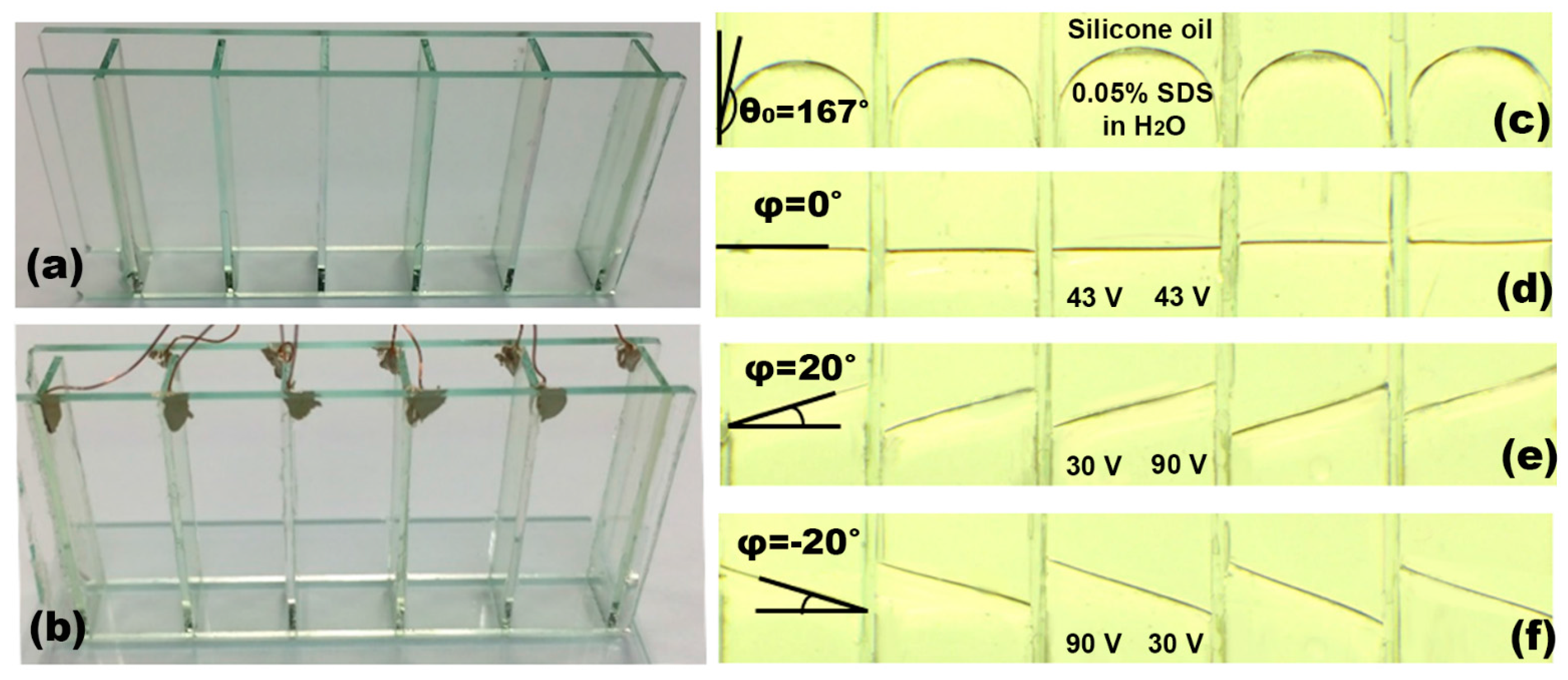
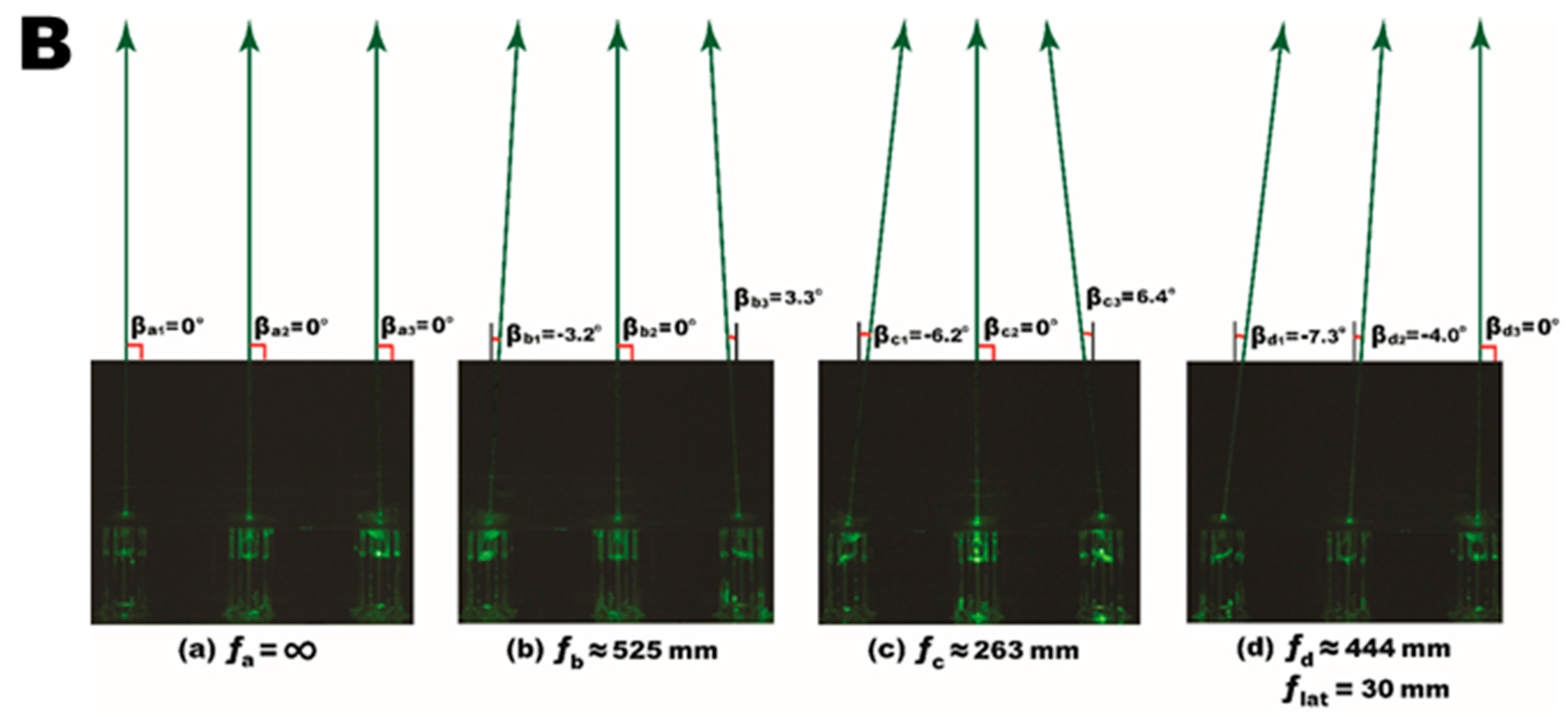
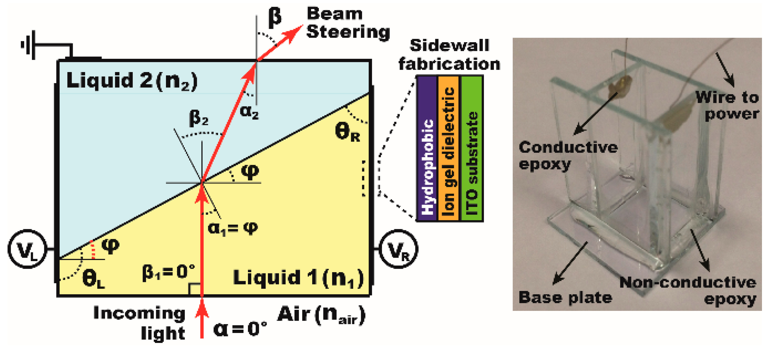
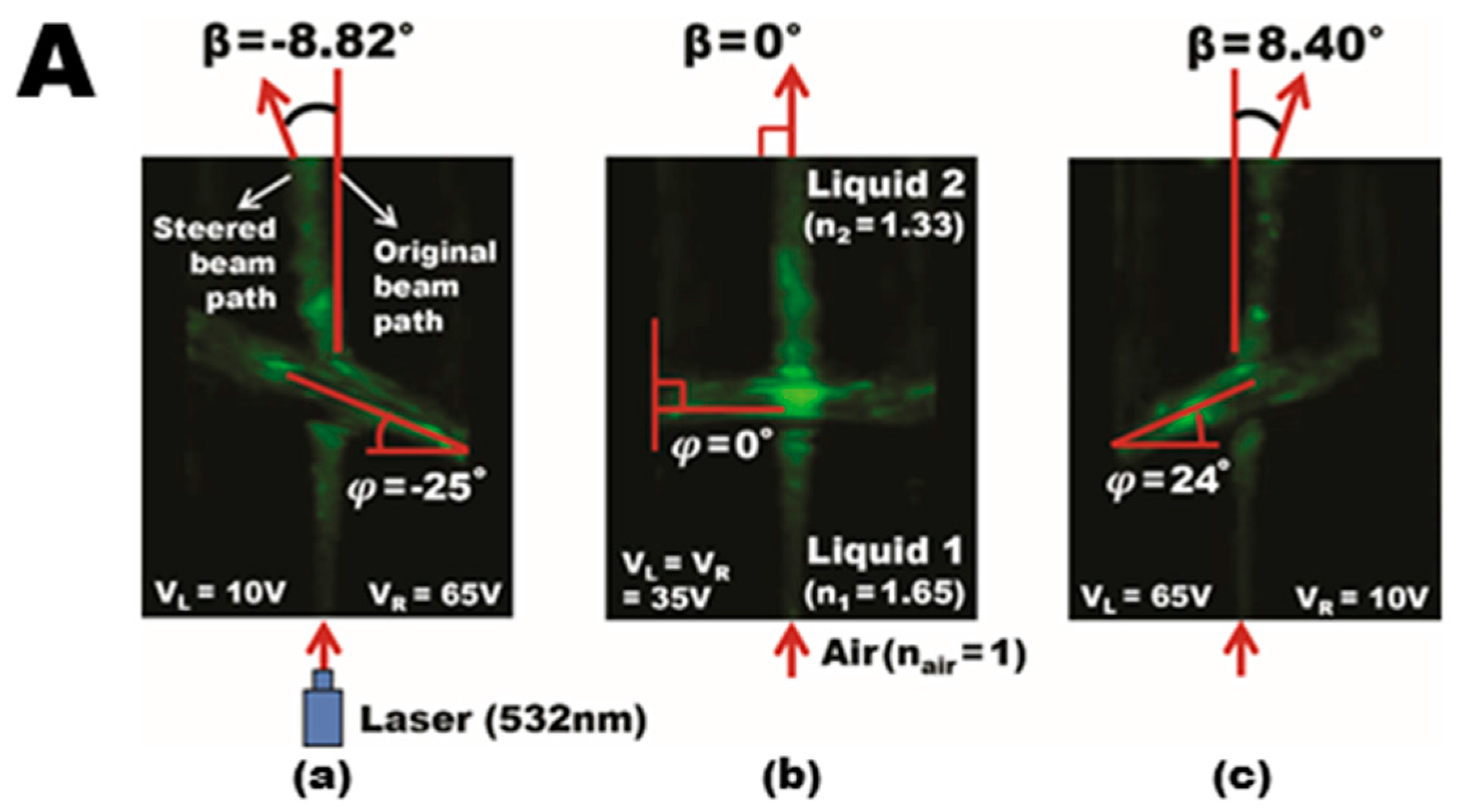
4.6. Demonstration of the Dip-Coatable Ion Gel for an Arrayed Prism as an Example of 3D EWOD Devices
5. Conclusions
Acknowledgments
Author Contributions
Conflicts of Interest
References
- Wheeler, A.R. Putting electrowetting to work. Science 2008, 322, 539–540. [Google Scholar] [CrossRef] [PubMed]
- Park, S.-Y.; Teitell, M.A.; Chiou, E.P.Y. Single-sided continuous optoelectrowetting (scoew) for droplet manipulation with light patterns. Lab Chip 2010, 10, 1655–1661. [Google Scholar] [CrossRef] [PubMed]
- Mugele, F.; Baret, J.-C. Electrowetting: From basics to applications. J. Phys. Condens. Matter 2005, 17, 705–774. [Google Scholar] [CrossRef]
- Narasimhan, V.; Park, S.-Y. An ion gel as a low-cost, spin-coatable, high-capacitance dielectric for electrowetting-on-dielectric (ewod). Langmuir 2015, 31, 8512–8518. [Google Scholar] [CrossRef] [PubMed]
- Chiou, P.Y.; Park, S.-Y.; Wu, M. Continuous optoelectrowetting (coew) for picoliter droplet manipulation. Appl. Phys. Lett. 2008, 22, 221110. [Google Scholar] [CrossRef]
- Vallet, M.; Berge, B.; Vovelle, L. Electrowetting of water and aqueous solutions on poly(ethylene terephthalate) insulating films. Polymer 1996, 37, 2465–2470. [Google Scholar] [CrossRef]
- Chang, J.-H.; Choi, D.Y.; Han, S.; Pak, J.J. Driving characteristics of the electrowetting-on-dielectric device using atomic-layer-deposited aluminum oxide as the dielectric. Microfluid. Nanofluid. 2010, 8, 269–273. [Google Scholar] [CrossRef]
- Lin, Y.-Y.; Welch, E.R.F.; Fair, R.B. Low voltage picoliter droplet manipulation utilizing electrowetting-on-dielectric platforms. Sens. Actuators B 2012, 173, 338–345. [Google Scholar] [CrossRef] [PubMed]
- Moon, H.; Cho, S.K.; Garrell, R.L.; Kim, C.-J. Low voltage electrowetting-on-dielectric. J. Appl. Phys. 2002, 92, 4080–4087. [Google Scholar] [CrossRef]
- Park, S.-Y.; Nam, Y. Single-sided digital microfluidic (sdmf) devices for effective coolant delivery and enhanced two-phase cooling. Micromachines 2017, 8, 3. [Google Scholar] [CrossRef]
- Abdelgawad, M.; Freire, S.L.S.; Yang, H.; Wheeler, A.R. All-terrain droplet actuation. Lab Chip 2008, 8, 672–677. [Google Scholar] [CrossRef] [PubMed]
- Fan, S.-K.; Yang, H.; Hsu, W. Droplet-on-a-wristband: Chip-to-chip digital microfluidic interfaces between replaceable and flexible electrowetting modules. Lab Chip 2011, 11, 343–347. [Google Scholar] [CrossRef] [PubMed]
- Jiang, D.; Park, S.-Y. Light-driven 3D droplet manipulation on flexible optoelectrowetting devices fabricated by a simple spin-coating method. Lab Chip 2016, 16, 1831–1839. [Google Scholar] [CrossRef] [PubMed]
- Lee, K.H.; Zhang, S.; Lodge, T.P.; Frisbie, C.D. Electrical impedance of spin-coatable ion gel films. J. Phys. Chem. B 2011, 115, 3315–3321. [Google Scholar] [CrossRef] [PubMed]
- Lee, K.H.; Kang, M.S.; Zhang, S.; Gu, Y.; Lodge, T.P.; Frisbie, C.D. “Cut and stick” rubbery ion gels as high capacitance gate dielectrics. Adv. Mater. 2012, 24, 4457–4462. [Google Scholar] [CrossRef] [PubMed]
- Galiński, M.; Lewandowski, A.; Stępniak, I. Ionic liquids as electrolytes. Electrochim. Acta 2006, 51, 5567–5580. [Google Scholar] [CrossRef]
- Ue, M.; Takeda, M.; Takahashi, T.; Takehara, M. Ionic liquids with low melting points and their application to double-layer capacitor electrolytes. Electrochem. Solid-State Lett. 2002, 5, A119–A121. [Google Scholar] [CrossRef]
- Smith, N.R.; Abeysinghe, D.C.; Haus, J.W.; Heikenfeld, J. Agile wide-angle beam steering with electrowetting microprisms. Opt. Express 2006, 14, 6557–6563. [Google Scholar] [CrossRef] [PubMed]
- Cheng, J.; Chen, C.-L. Adaptive beam tracking and steering via electrowetting-controlled liquid prism. Appl. Phys. Lett. 2011, 99, 191108. [Google Scholar] [CrossRef]
- Boer, B.D.; Suijver, F.; Megens, M.; Deladi, S.; Kuiper, S. Control of an electrowetting-based beam deflector. J. Appl. Phys. 2010, 107, 063101. [Google Scholar] [CrossRef]
- Lee, D.-G.; Park, J.; Bae, J.; Kim, H.-Y. Dynamics of a microliquid prism actuated by electrowetting. Lab Chip 2013, 13, 274–279. [Google Scholar] [CrossRef] [PubMed]
- Clement, C.E.; Park, S.-Y. High-performance beam steering using electrowetting-driven liquid prism fabricated by a simple dip-coating method. Appl. Phys. Lett. 2016, 108, 191601. [Google Scholar] [CrossRef]
- Clement, C.; Thio, S.K.; Park, S.-Y. An optofluidic tunable fresnel lens for spatial focal control based on electrowetting-on-dielectric (ewod). Sens. Actuators B 2017, 240, 909–915. [Google Scholar] [CrossRef]
- Narasimhan, V.; Jiang, D.; Park, S.-Y. Design and optical analyses of an arrayed microfluidic tunable prism panel for enhancing solar energy collection. Appl. Energy 2016, 162, 450–459. [Google Scholar] [CrossRef]
- Jiang, D.; Park, S.-Y. Microfluidic-guided solar indoor lighting system. In Proceedings of the 6th International Multidisciplinary Conference on Optofluidics, Beijing, China, 24–27 July 2016.
- Cheng, J.; Park, S.-Y.; Chen, C.-L. Optofluidic solar concentrators using electrowetting tracking: Concept, design, and characterization. Sol. Energy 2013, 89, 152–167. [Google Scholar] [CrossRef]
- Seow, Y.C.; Lim, S.P.; Lee, H.P. Optofluidic variable-focus lenses for light manipulation. Lab Chip 2012, 12, 3810–3815. [Google Scholar] [CrossRef] [PubMed]
- Song, W.; Psaltis, D. Electrically tunable optofluidic light switch for reconfigurable solar lighting. Lab Chip 2013, 13, 2708–2713. [Google Scholar] [CrossRef] [PubMed]
- Landau, L.; Levich, B. Dragging of a liquid by a moving plate. Acta Physicochim. URSS 1942, XVII, 42–58. [Google Scholar]
- Pu, J.; Yomogida, Y.; Liu, K.-K.; Li, L.-J.; Iwasa, Y.; Takenobu, T. Highly flexible mos2 thin-film transistors with ion gel dielectrics. Nano Lett. 2012, 12, 4013–4017. [Google Scholar] [CrossRef] [PubMed]
- Lee, J.; Panzer, M.J.; He, Y.; Lodge, T.P.; Frisbie, C.D. Ion gel gated polymer thin-film transistors. J. Am. Chem. Soc. 2007, 129, 4532–4533. [Google Scholar] [CrossRef] [PubMed]
- Zhang, S.; Lee, K.H.; Frisbie, D.; Lodge, T.P. Ionic conductivity, capacitance, and viscoelastic properties of block copolymer-based ion gels. Macromolecules 2011, 44, 940–949. [Google Scholar] [CrossRef]
- Yuan, H.; Liu, H.; Shimotani, H.; Guo, H.; Chen, M.; Xue, Q.; Iwasa, Y. Liquid-gated ambipolar transport in ultrathin films of a topological insulator bi2te3. Nano Lett. 2011, 11, 2601–2605. [Google Scholar] [CrossRef] [PubMed]
- Cho, J.H.; Lee, J.; Xia, Y.; Kim, B.; He, Y.; Renn, M.J.; Lodge, T.P.; Frisbie, C.D. Printable ion-gel gate dielectrics for low-voltage polymer thin-film transistors on plastic. Nat. Mater. 2008, 7, 900–906. [Google Scholar] [CrossRef] [PubMed]
- Jansen, J.C.; Friess, K.; Clarizia, G.; Schauer, J.; Izák, P. High ionic liquid content polymeric gel membranes: Preparation and performance. Macromolecules 2011, 44, 39–45. [Google Scholar] [CrossRef]
- Karim, A.; Slawecki, T.M.; Kumar, S.K.; Douglas, J.F.; Satija, S.K.; Han, C.C.; Russell, T.P.; Liu, Y.; Overney, R.; Sokolov, J.; et al. Phase-separation-induced surface patterns in thin polymer blend films. Macromolecules 1998, 31, 857–862. [Google Scholar] [CrossRef]
- Berry, S.; Kedzierski, J.; Abedian, B. Irreversible electrowetting on thin fluoropolymer films. Langmuir 2007, 23, 12429–12435. [Google Scholar] [CrossRef] [PubMed]
- Berry, S.; Kedzierski, J.; Abedian, B. Low voltage electrowetting using thin fluoroploymer films. J. Colloid Interface Sci. 2006, 303, 517–527. [Google Scholar] [CrossRef] [PubMed]
- Zhang, J.; Meter, D.V.; Hou, L.; Smith, N.; Yang, J.; Stalcup, A.; Laughlin, R.; Heikenfeld, J. Preparation and analysis of 1-chloronaphthalene for highly refractive electrowetting optics. Langmuir 2009, 25, 10413–10416. [Google Scholar] [CrossRef] [PubMed]


© 2017 by the authors. Licensee MDPI, Basel, Switzerland. This article is an open access article distributed under the terms and conditions of the Creative Commons Attribution (CC-BY) license ( http://creativecommons.org/licenses/by/4.0/).
Share and Cite
Clement, C.E.; Jiang, D.; Thio, S.K.; Park, S.-Y. A Study of Dip-Coatable, High-Capacitance Ion Gel Dielectrics for 3D EWOD Device Fabrication. Materials 2017, 10, 41. https://doi.org/10.3390/ma10010041
Clement CE, Jiang D, Thio SK, Park S-Y. A Study of Dip-Coatable, High-Capacitance Ion Gel Dielectrics for 3D EWOD Device Fabrication. Materials. 2017; 10(1):41. https://doi.org/10.3390/ma10010041
Chicago/Turabian StyleClement, Carlos E., Dongyue Jiang, Si Kuan Thio, and Sung-Yong Park. 2017. "A Study of Dip-Coatable, High-Capacitance Ion Gel Dielectrics for 3D EWOD Device Fabrication" Materials 10, no. 1: 41. https://doi.org/10.3390/ma10010041