
Synthesis of Graphene Based Membranes: Effect of Substrate Surface Properties on Monolayer Graphene Transfer

Abstract
:1. Introduction
2. Materials and Methods
2.1. Materials
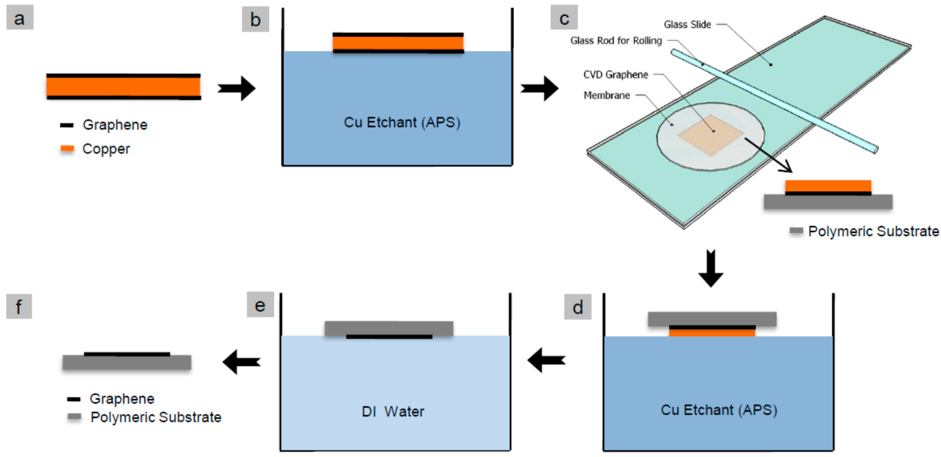
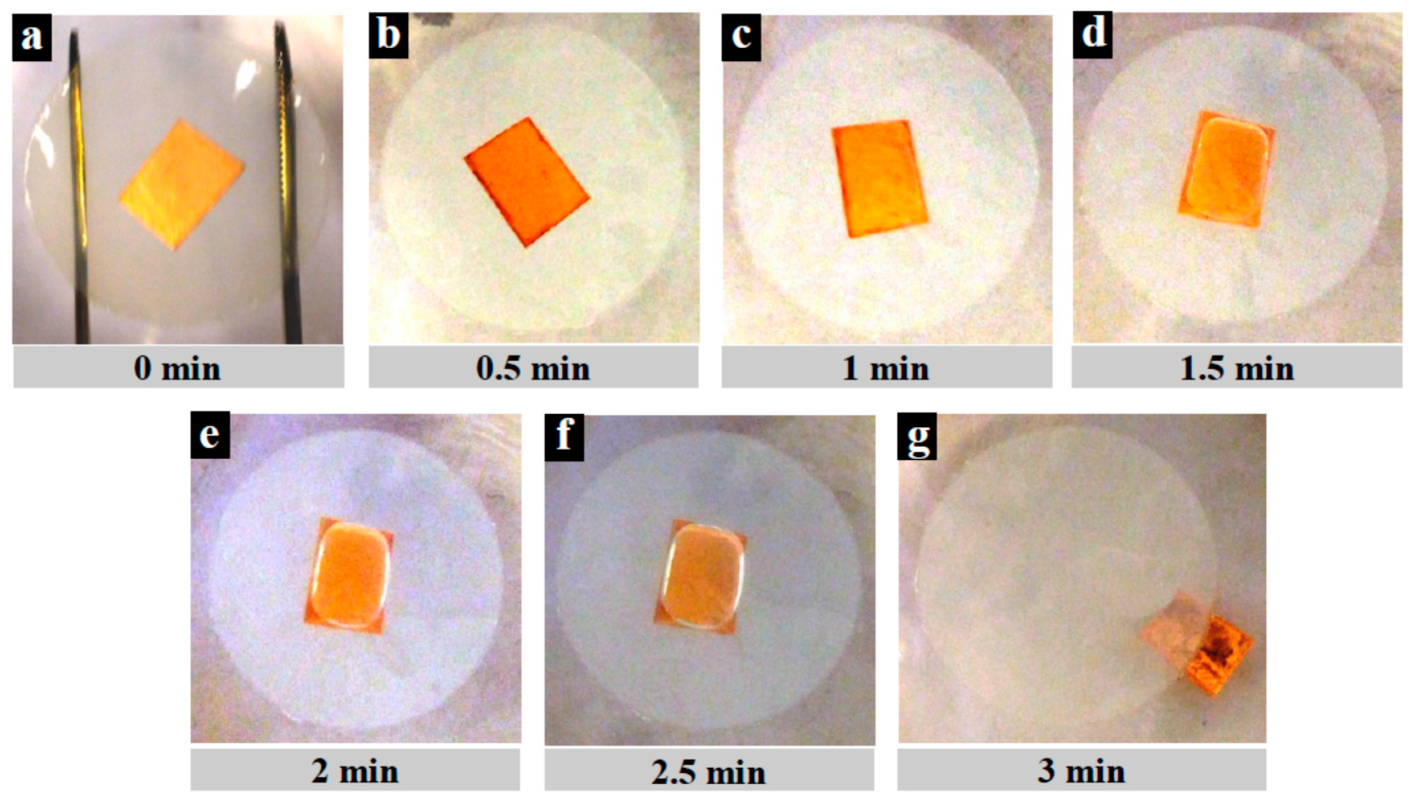
2.2. Monolayer Graphene Transfer Process
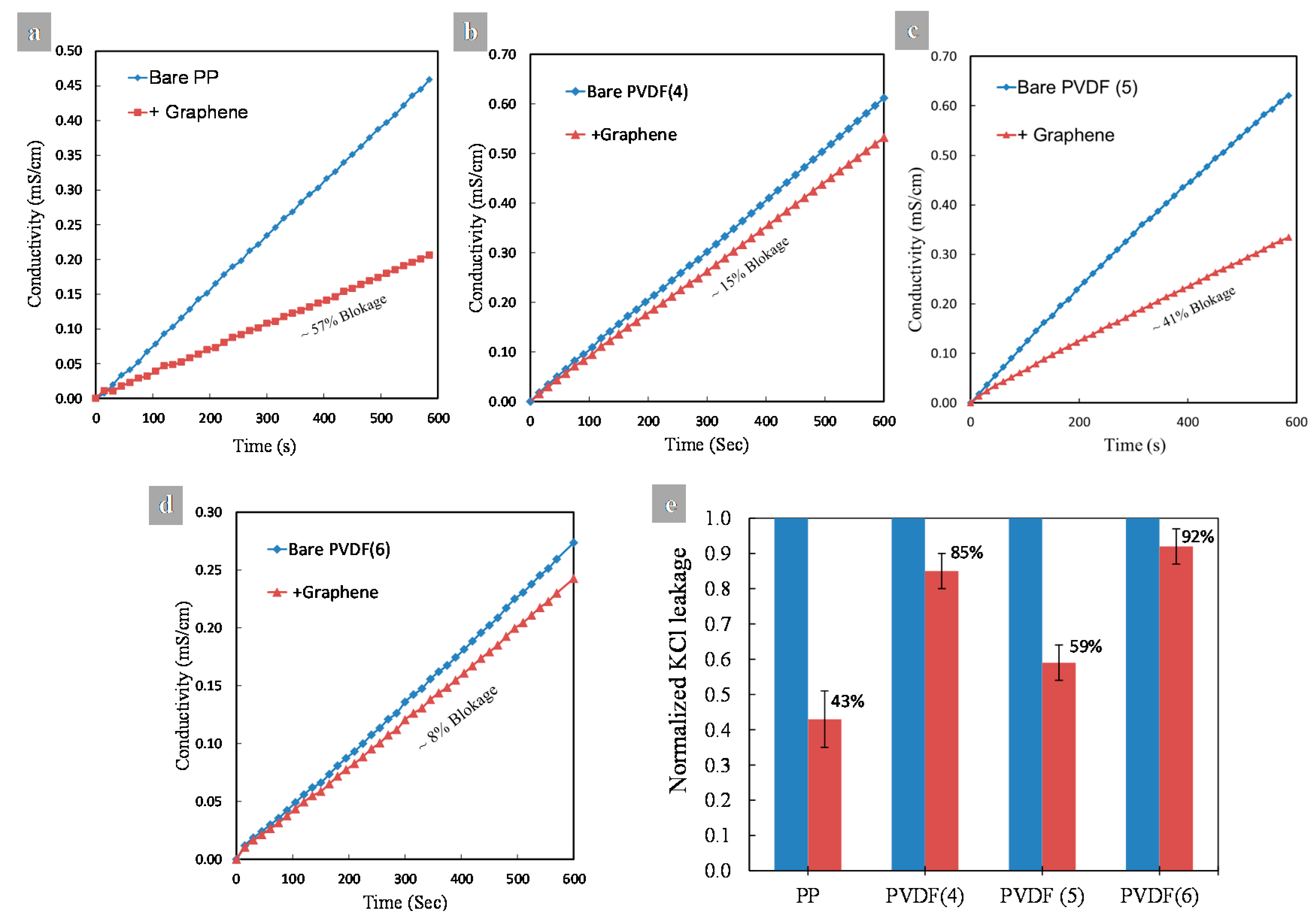
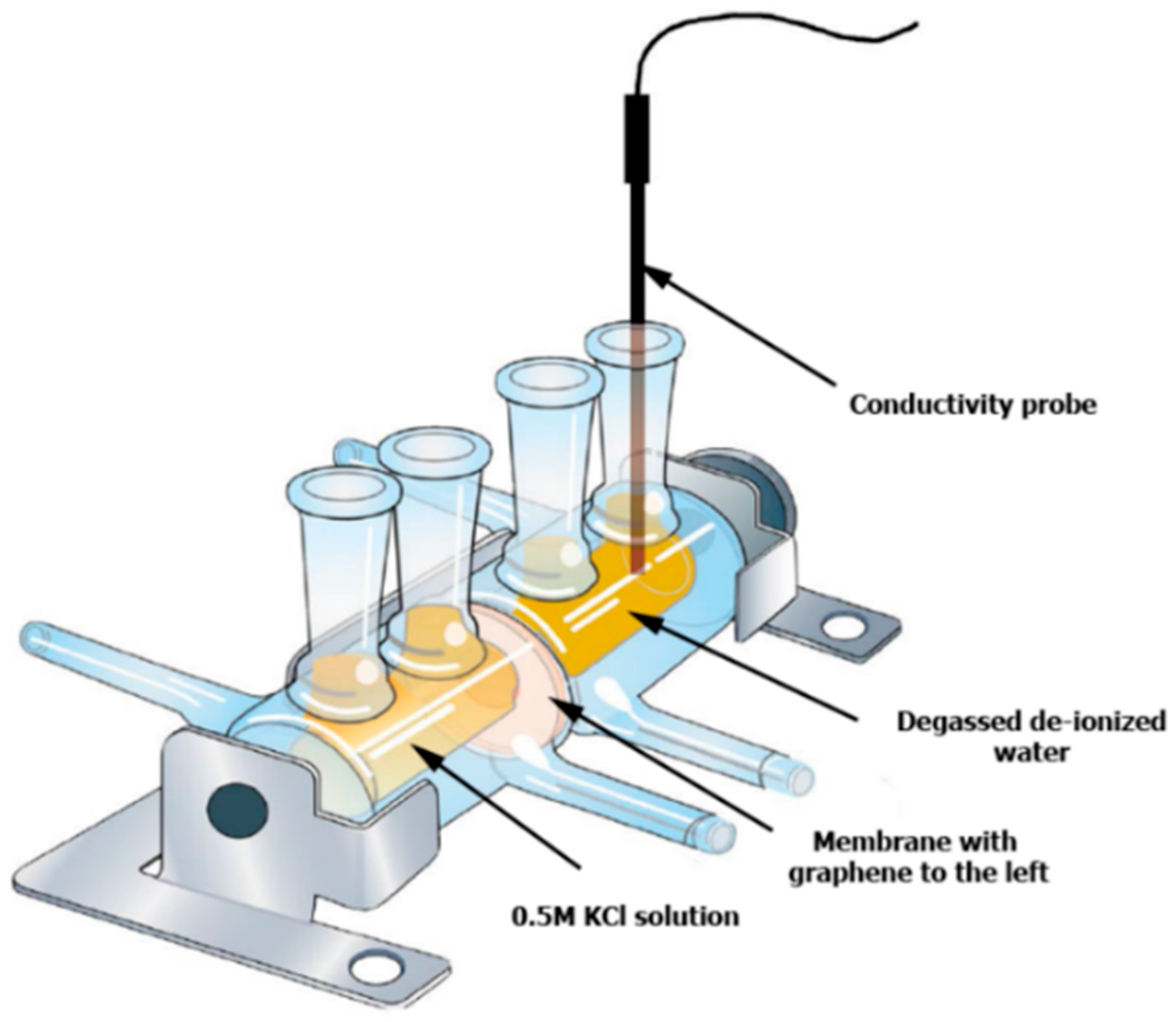
2.3. Ionic Transport Study
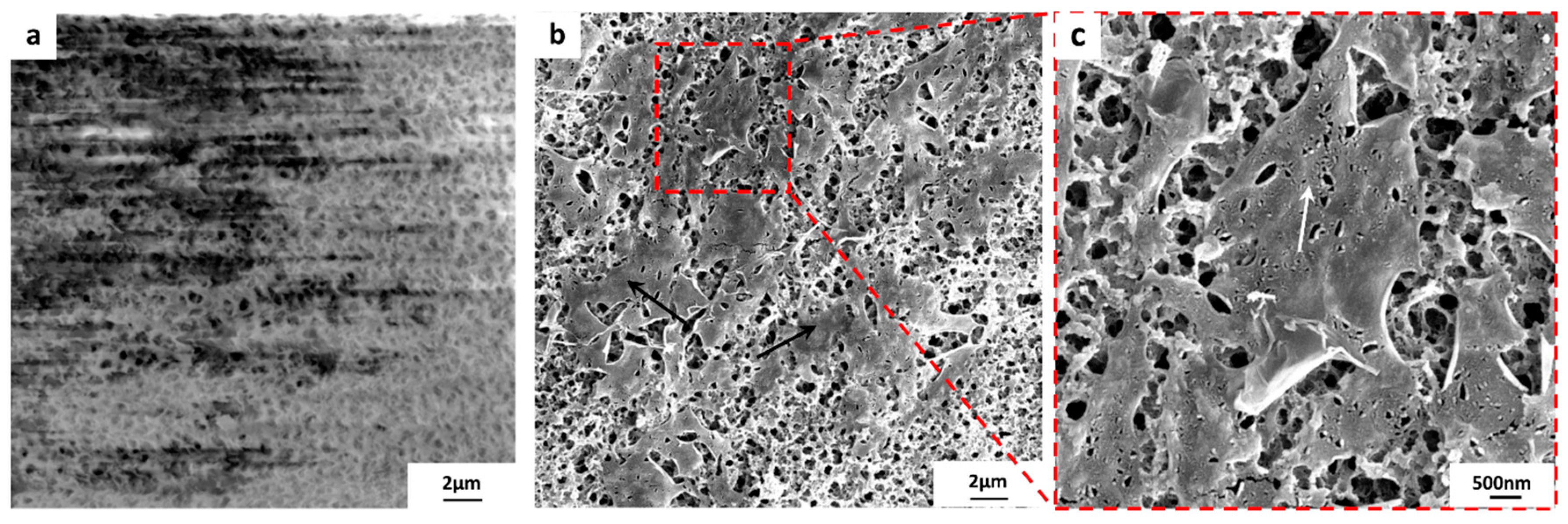
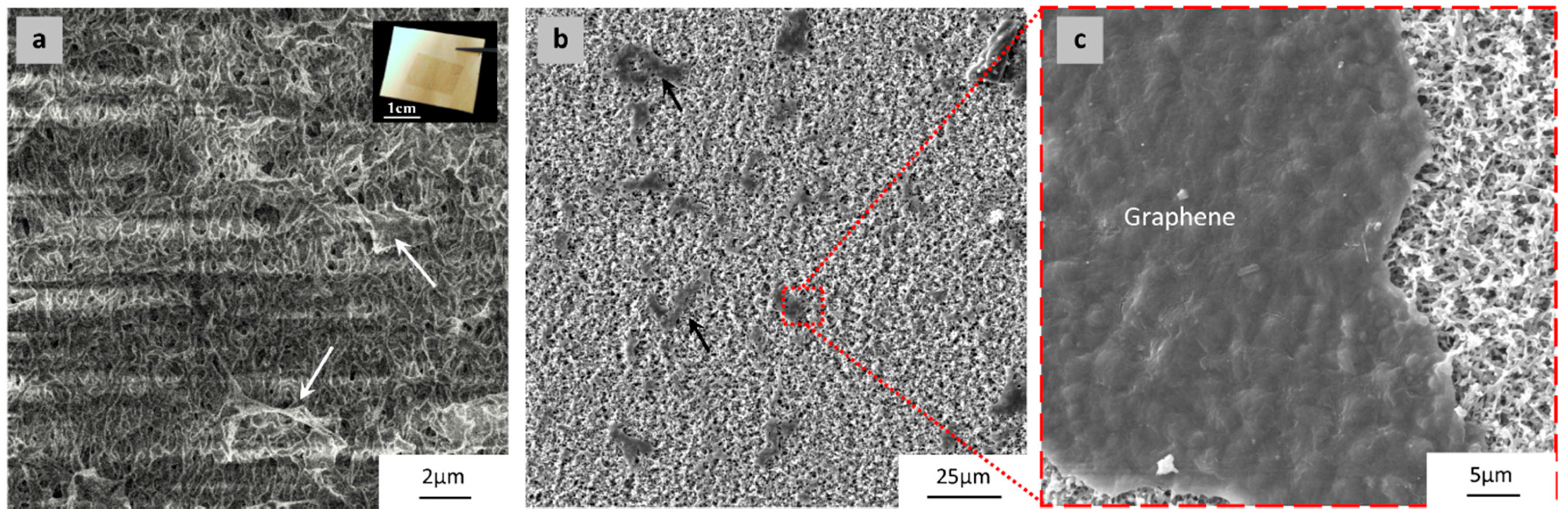
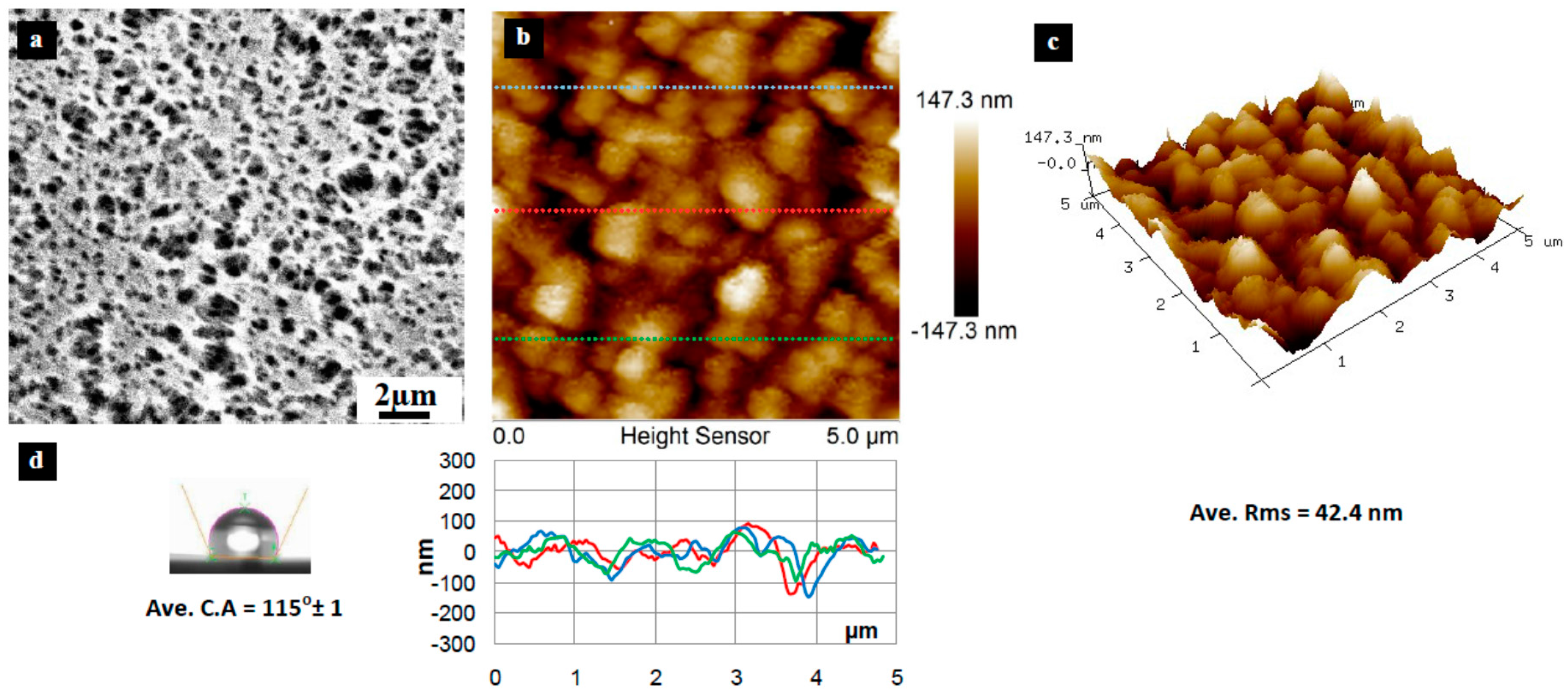
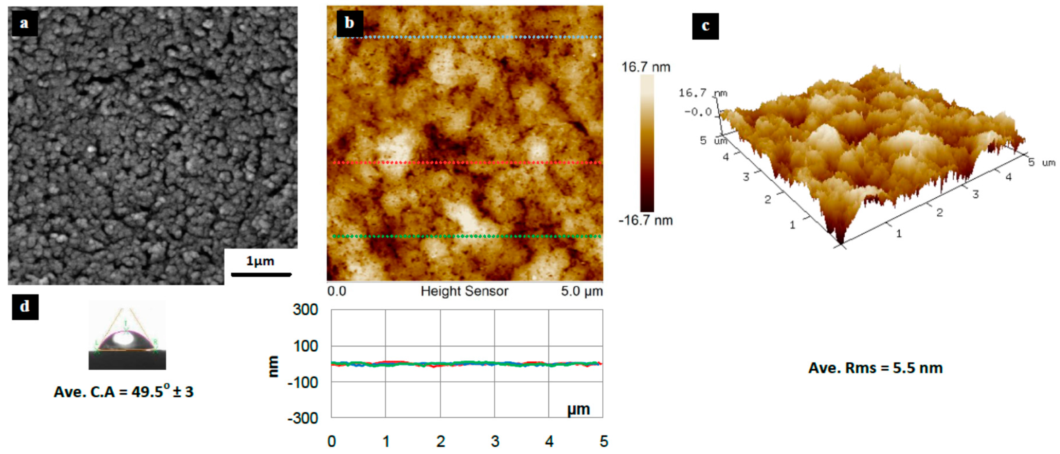
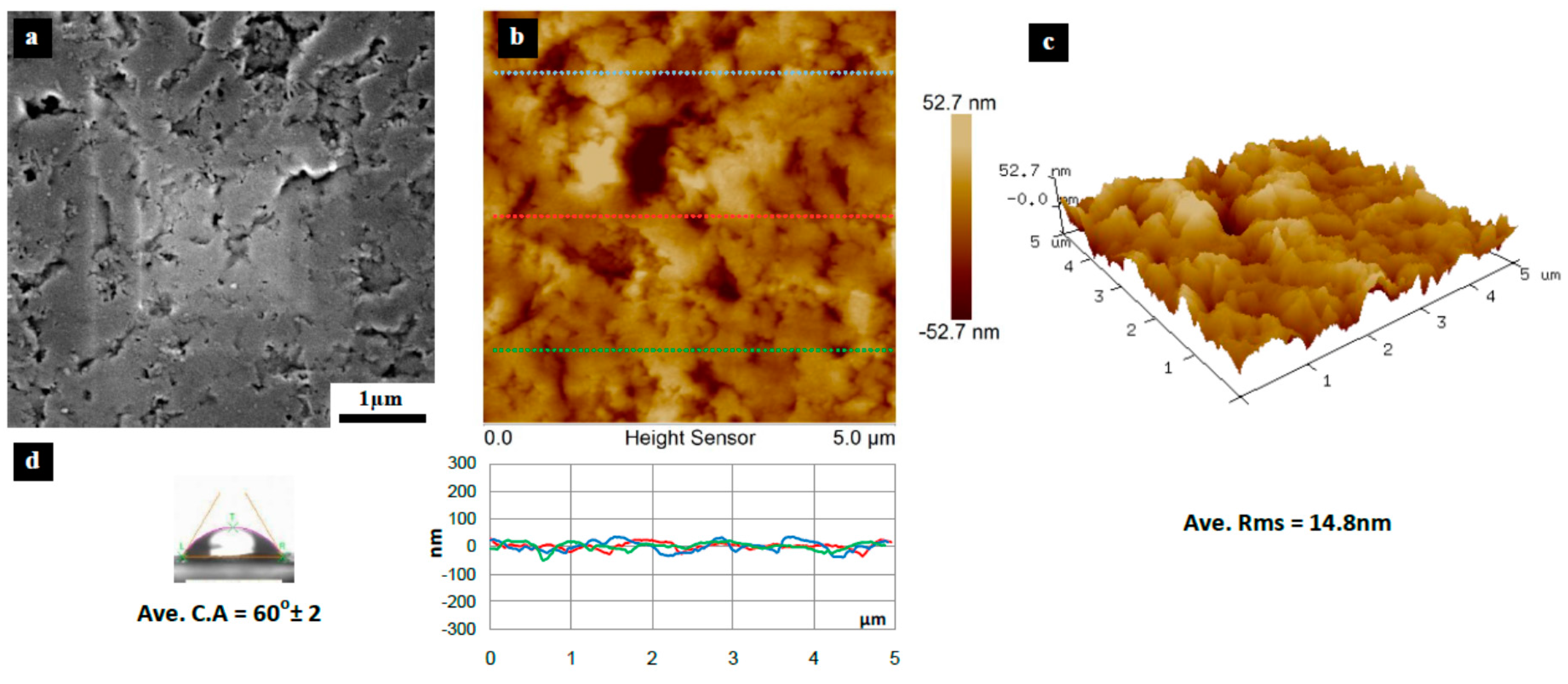
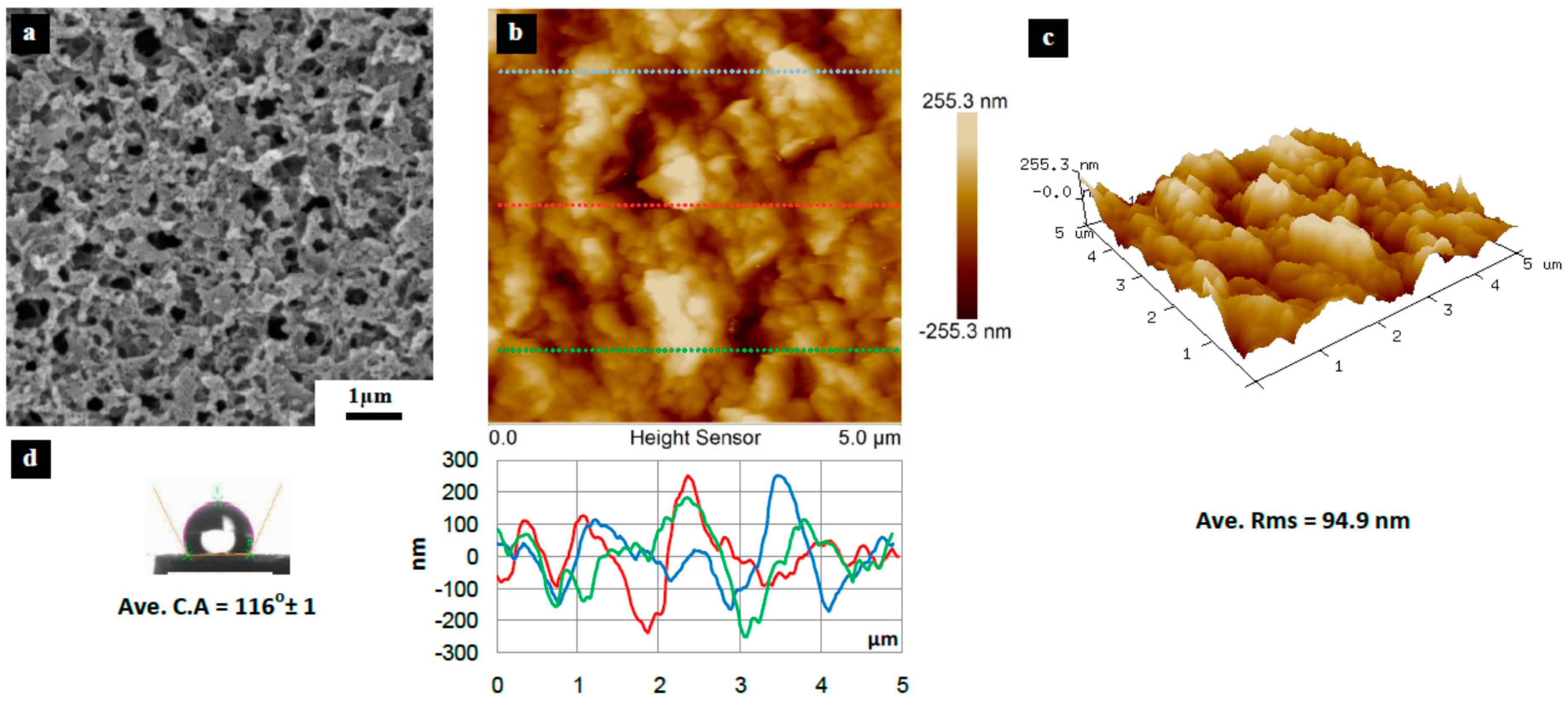
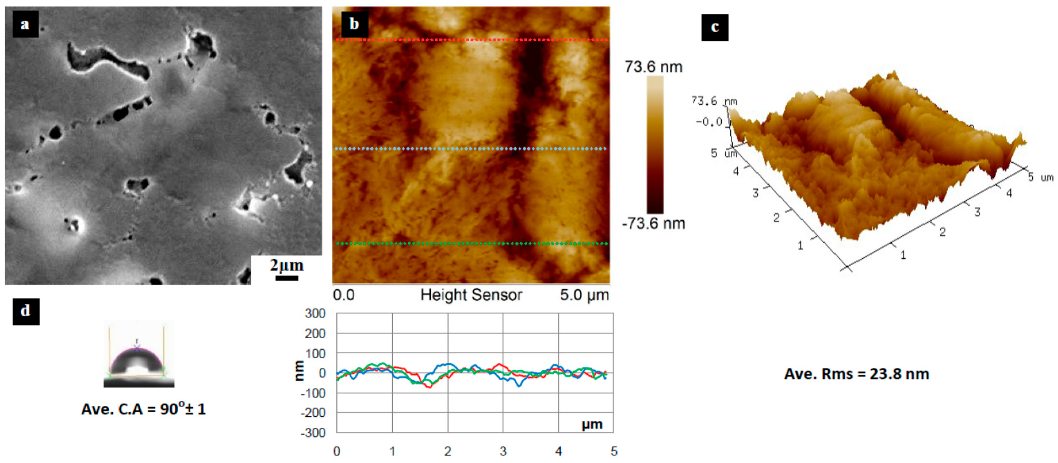
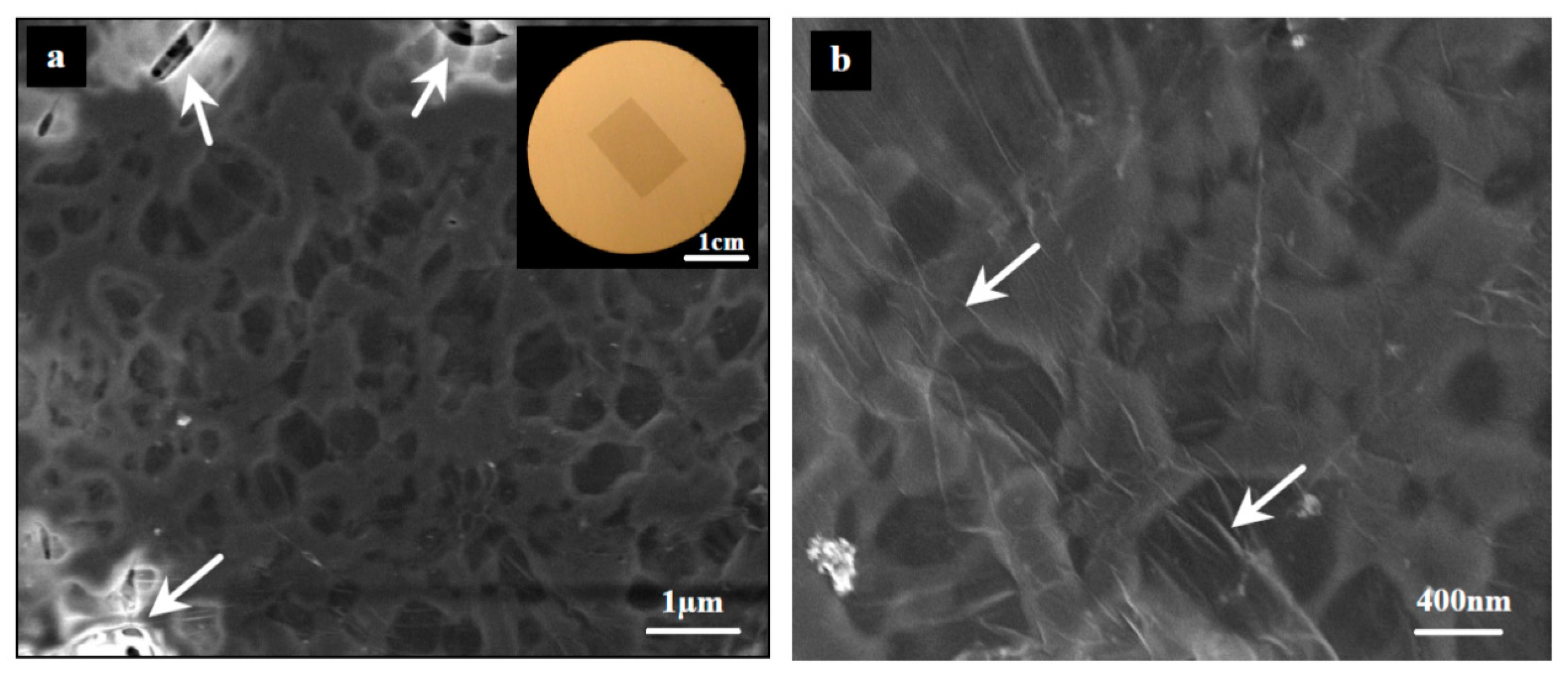
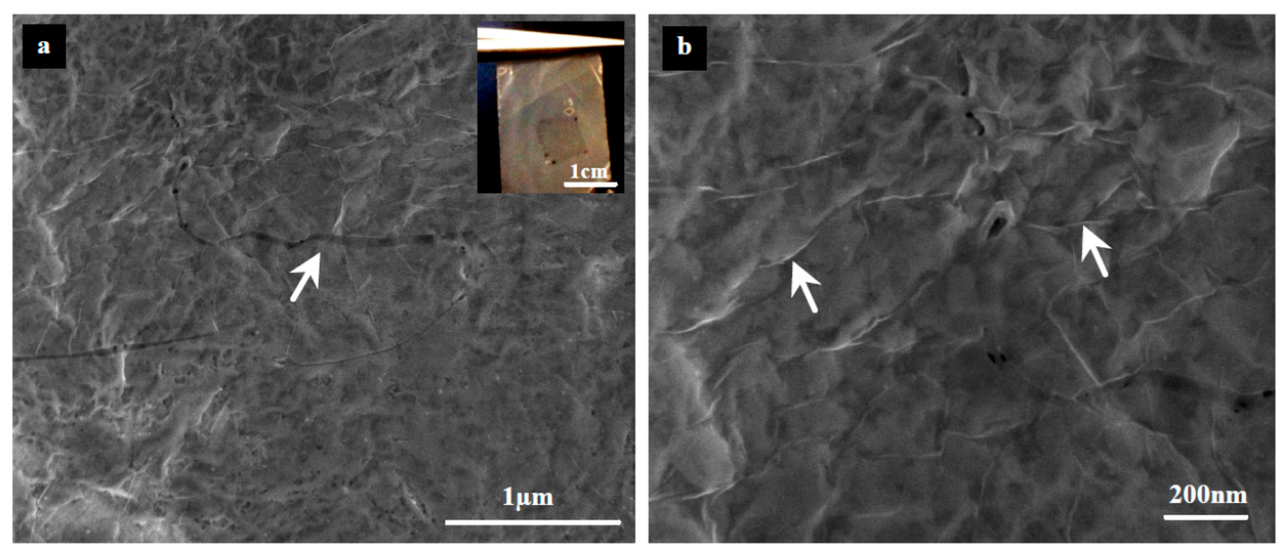
3. Results and Discussion
Graphene Transfer onto Polymeric Substrates
4. Conclusions
Supplementary Materials
Acknowledgments
Author Contributions
Conflicts of Interest
References
- Ranjbartoreh, A.R.; Wang, B.; Shen, X.; Wang, G. Advanced mechanical properties of graphene paper. J. Appl. Phys. 2011, 109. [Google Scholar] [CrossRef]
- Lee, C.; Wei, X.; Kysar, J.W.; Hone, J. Measurement of the elastic properties and intrinsic strength of monolayer graphene. Science 2008, 321, 385–388. [Google Scholar] [CrossRef] [PubMed]
- Hwang, E.H.; Adam, S.; Sarma, S.D. Carrier transport in two-dimensional graphene layers. Phys. Rev. Lett. 2007, 98. [Google Scholar] [CrossRef] [PubMed]
- Kumar, P.; Singh, A.K.; Hussain, S.; Hui, K.N.; San Hui, K.; Eom, J.; Jung, J.; Singh, J. Graphene: Synthesis, properties and application in transparent electronic devices. Rev. Adv. Sci. Eng. 2013, 2, 238–258. [Google Scholar] [CrossRef]
- Balandin, A.A.; Ghosh, S.; Bao, W.; Calizo, I.; Teweldebrhan, D.; Miao, F.; Lau, C.N. Superior thermal conductivity of single-layer graphene. Nano Lett. 2008, 8, 902–907. [Google Scholar] [CrossRef] [PubMed]
- Balandin, A.; Ghosh, S.; Bao, W.; Calizo, I.; Teweldebrhan, D.; Miao, F.; Lau, C. Extremely high thermal conductivity of graphene: Experimental study. arXiv 2008. [Google Scholar]
- Shou-En, Z.; Shengjun, Y.; Janssen, G.C.A.M. Optical transmittance of multilayer graphene. Europhys. Lett. 2014, 108. [Google Scholar] [CrossRef]
- Falkovsky, L. Optical properties of grapheme. J. Phys. Conf. Ser. 2008, 129, 012004. [Google Scholar] [CrossRef]
- Stöberl, U.; Wurstbauer, U.; Wegscheider, W.; Weiss, D.; Eroms, J. Morphology and flexibility of graphene and few-layer graphene on various substrates. Appl. Phys. Lett. 2008, 93. [Google Scholar] [CrossRef]
- Despres, J.; Daguerre, E.; Lafdi, K. Flexibility of graphene layers in carbon nanotubes. Carbon Nanotub. 1996, 149, 1–2. [Google Scholar]
- Novoselov, K.S.; Fal, V.; Colombo, L.; Gellert, P.; Schwab, M.; Kim, K. A roadmap for graphene. Nature 2012, 490, 192–200. [Google Scholar] [CrossRef] [PubMed]
- Ponomarenko, L.A.; Schedin, F.; Katsnelson, M.I.; Yang, R.; Hill, E.W.; Novoselov, K.S.; Geim, A.K. Chaotic dirac billiard in graphene quantum dots. Science 2008, 320, 356–358. [Google Scholar] [CrossRef] [PubMed]
- Wisitsoraat, A.; Tuantranont, A. Graphene-based chemical and biosensors. In Applications of Nanomaterials in Sensors and Diagnostics; Springer: New York, NY, USA, 2013; pp. 103–141. [Google Scholar]
- Wang, X.; Zhi, L.; Müllen, K. Transparent, conductive graphene electrodes for dye-sensitized solar cells. Nano Lett. 2008, 8, 323–327. [Google Scholar] [CrossRef] [PubMed]
- Park, H.; Brown, P.R.; Bulović, V.; Kong, J. Graphene as transparent conducting electrodes in organic photovoltaics: Studies in graphene morphology, hole transporting layers, and counter electrodes. Nano Lett. 2011, 12, 133–140. [Google Scholar] [CrossRef] [PubMed]
- Sensale-Rodriguez, B. Graphene-based optoelectronics. J. Lightwave Technol. 2015, 33, 1100–1108. [Google Scholar] [CrossRef]
- Koppens, F. Graphene nano-optoelectronics. In CLEO: QELS_Fundamental Science; Optical Society of America: Washington, DC, USA, 2013. [Google Scholar]
- Bonaccorso, F.; Sun, Z.; Hasan, T.; Ferrari, A. Graphene photonics and optoelectronics. Nat. Photonics 2010, 4, 611–622. [Google Scholar] [CrossRef]
- Lalwani, G.; Henslee, A.M.; Farshid, B.; Lin, L.; Kasper, F.K.; Qin, Y.-X.; Mikos, A.G.; Sitharaman, B. Two-dimensional nanostructure- reinforced biodegradable polymeric nanocomposites for bone tissue engineering. Biomacromolecules 2013, 14, 900–909. [Google Scholar] [CrossRef] [PubMed]
- Tkacz, R.; Oldenbourg, R.; Mehta, S.B.; Miansari, M.; Verma, A.; Majumder, M. pH dependent isotropic to nematic phase transitions in graphene oxide dispersions reveal droplet liquid crystalline phases. Chem. Commun. 2014, 50, 6668–6671. [Google Scholar] [CrossRef] [PubMed]
- Hedberg, J. Graphene-Based Solar Cells Could Yield 60% Efficiency; Institute of Photonic Sciences: Barcelona, Spain, 2013. [Google Scholar]
- Hu, S.; Lozada-Hidalgo, M.; Wang, F.C.; Mishchenko, A.; Schedin, F.; Nair, R.R.; Hill, E.W.; Boukhvalov, D.W.; Katsnelson, M.I.; Dryfe, R.A.W.; et al. Proton transport through one-atom-thick crystals. Nature 2014, 516, 227–230. [Google Scholar] [CrossRef] [PubMed]
- Peng, Z.; Lin, J.; Ye, R.; Samuel, E.L.G.; Tour, J.M. Flexible and stackable laser-induced graphene supercapacitors. ACS Appl. Mater. Interfaces 2015, 7, 3414–3419. [Google Scholar] [CrossRef] [PubMed]
- Zhu, S.; Li, T. Hydrogenation-assisted graphene origami and its application in programmable molecular mass uptake, storage, and release. ACS Nano 2014, 8, 2864–2872. [Google Scholar] [CrossRef] [PubMed]
- Andronico, M. 5 ways graphene will change gadgets forever. Laptop. 2014. Available online: http://www.laptopmag.com/articles/graphene-tech-uses (accessed on 19 January 2017).
- O’Hern, S.C.; Boutilier, M.S.H.; Idrobo, J.-C.; Song, Y.; Kong, J.; Laoui, T.; Atieh, M.; Karnik, R. Selective ionic transport through tunable subnanometer pores in single-layer graphene membranes. Nano Lett. 2014, 14, 1234–1241. [Google Scholar] [CrossRef] [PubMed]
- Meyer, J.C.; Geim, A.K.; Katsnelson, M.; Novoselov, K.; Booth, T.; Roth, S. The structure of suspended graphene sheets. Nature 2007, 446, 60–63. [Google Scholar] [CrossRef] [PubMed] [Green Version]
- Geim, A.K.; Novoselov, K.S. The rise of graphene. Nat. Mater. 2007, 6, 183–191. [Google Scholar] [CrossRef] [PubMed]
- Stankovich, S.; Dikin, D.A.; Dommett, G.H.; Kohlhaas, K.M.; Zimney, E.J.; Stach, E.A.; Piner, R.D.; Nguyen, S.T.; Ruoff, R.S. Graphene-based composite materials. Nature 2006, 442, 282–286. [Google Scholar] [CrossRef] [PubMed]
- Watcharotone, S.; Dikin, D.A.; Stankovich, S.; Piner, R.; Jung, I.; Dommett, G.H.; Evmenenko, G.; Wu, S.-E.; Chen, S.-F.; Liu, C.-P. Graphene-silica composite thin films as transparent conductors. Nano Lett. 2007, 7, 1888–1892. [Google Scholar] [CrossRef] [PubMed]
- Dikin, D.A.; Stankovich, S.; Zimney, E.J.; Piner, R.D.; Dommett, G.H.; Evmenenko, G.; Nguyen, S.T.; Ruoff, R.S. Preparation and characterization of graphene oxide paper. Nature 2007, 448, 457–460. [Google Scholar] [CrossRef] [PubMed]
- Kim, K.S.; Zhao, Y.; Jang, H.; Lee, S.Y.; Kim, J.M.; Kim, K.S.; Ahn, J.-H.; Kim, P.; Choi, J.-Y.; Hong, B.H. Large-scale pattern growth of graphene films for stretchable transparent electrodes. Nature 2009, 457, 706–710. [Google Scholar] [CrossRef] [PubMed]
- Park, S.; Ruoff, R.S. Chemical methods for the production of graphenes. Nat. Nanotechnol. 2009, 4, 217–224. [Google Scholar] [CrossRef] [PubMed]
- Li, X.; Cai, W.; An, J.; Kim, S.; Nah, J.; Yang, D.; Piner, R.; Velamakanni, A.; Jung, I.; Tutuc, E. Large-area synthesis of high-quality and uniform graphene films on copper foils. Science 2009, 324, 1312–1314. [Google Scholar] [CrossRef] [PubMed]
- Kosynkin, D.V.; Higginbotham, A.L.; Sinitskii, A.; Lomeda, J.R.; Dimiev, A.; Price, B.K.; Tour, J.M. Longitudinal unzipping of carbon nanotubes to form graphene nanoribbons. Nature 2009, 458, 872–876. [Google Scholar] [CrossRef] [PubMed]
- Brownson, D.A.; Banks, C.E. The electrochemistry of CVD graphene: Progress and prospects. Phys. Chem. Chem. Phys. 2012, 14, 8264–8281. [Google Scholar] [CrossRef] [PubMed]
- Soldano, C.; Mahmood, A.; Dujardin, E. Production, properties and potential of graphene. Carbon 2010, 48, 2127–2150. [Google Scholar] [CrossRef]
- Li, X.; Magnuson, C.W.; Venugopal, A.; An, J.; Suk, J.W.; Han, B.; Borysiak, M.; Cai, W.; Velamakanni, A.; Zhu, Y. Graphene films with large domain size by a two-step chemical vapor deposition process. Nano Lett. 2010, 10, 4328–4334. [Google Scholar] [CrossRef] [PubMed]
- Rümmeli, M.H.; Rocha, C.G.; Ortmann, F.; Ibrahim, I.; Sevincli, H.; Börrnert, F.; Kunstmann, J.; Bachmatiuk, A.; Pötschke, M.; Shiraishi, M. Graphene: Piecing it together. Adv. Mater. 2011, 23, 4471–4490. [Google Scholar] [CrossRef] [PubMed] [Green Version]
- Ghoneim, M.T. Efficient Transfer of Graphene-Physical and Electrical Performance Perspective. Master’s Thesis, King Abdullah University of Science and Technology, Thuwal, Saudi Arabia, 2012. [Google Scholar]
- Mattevi, C.; Kim, H.; Chhowalla, M. A review of chemical vapour deposition of graphene on copper. J. Mater. Chem. 2011, 21, 3324–3334. [Google Scholar] [CrossRef]
- Li, X.; Cai, W.; Jung, I.H.; An, J.H.; Yang, D.; Velamakanni, A.; Piner, R.; Colombo, L.; Ruoff, R.S. Synthesis, characterization, and properties of large-area graphene films. ECS Trans. 2009, 19, 41–52. [Google Scholar]
- Reina, A.; Jia, X.; Ho, J.; Nezich, D.; Son, H.; Bulovic, V.; Dresselhaus, M.S.; Kong, J. Large area, few-layer graphene films on arbitrary substrates by chemical vapor deposition. Nano Lett. 2008, 9, 30–35. [Google Scholar] [CrossRef] [PubMed]
- Li, W.; Tan, C.; Lowe, M.A.; Abruna, H.D.; Ralph, D.C. Electrochemistry of individual monolayer graphene sheets. ACS Nano 2011, 5, 2264–2270. [Google Scholar] [CrossRef] [PubMed]
- Li, X.; Zhu, Y.; Cai, W.; Borysiak, M.; Han, B.; Chen, D.; Piner, R.D.; Colombo, L.; Ruoff, R.S. Transfer of large-area graphene films for high-performance transparent conductive electrodes. Nano Lett. 2009, 9, 4359–4363. [Google Scholar] [CrossRef] [PubMed]
- Kafiah, F.M.; Khan, Z.; Ibrahim, A.; Karnik, R.; Atieh, M.; Laoui, T. Monolayer graphene transfer onto polypropylene and polyvinylidenedifluoride microfiltration membranes for water desalination. Desalination 2016, 388, 29–37. [Google Scholar] [CrossRef]
- Regan, W.; Alem, N.; Alemán, B.; Geng, B.; Girit, Ç.; Maserati, L.; Wang, F.; Crommie, M.; Zettl, A. A direct transfer of layer-area graphene. Appl. Phys. Lett. 2010, 96. [Google Scholar] [CrossRef]
- Bae, S.; Kim, H.; Lee, Y.; Xu, X.; Park, J.-S.; Zheng, Y.; Balakrishnan, J.; Lei, T.; Kim, H.R.; Song, Y.I. Roll-to-roll production of 30-inch graphene films for transparent electrodes. Nat. Nanotechnol. 2010, 5, 574–578. [Google Scholar] [CrossRef] [PubMed]
- Bunch, J.S.; Dunn, M.L. Adhesion mechanics of graphene membranes. Solid State Commun. 2012, 152, 1359–1364. [Google Scholar] [CrossRef]
- Martins, L.G.; Song, Y.; Zeng, T.; Dresselhaus, M.S.; Kong, J.; Araujo, P.T. Direct transfer of graphene onto flexible substrates. Proc. Natl. Acad. Sci. USA 2013, 110, 17762–17767. [Google Scholar] [CrossRef] [PubMed]
- O’Hern, S.C.; Stewart, C.A.; Boutilier, M.S.; Idrobo, J.C.; Bhaviripudi, S.; Das, S.K.; Kong, J.; Laoui, T.; Atieh, M.; Karnik, R. Selective molecular transport through intrinsic defects in a single layer of CVD graphene. ACS Nano 2012, 6, 10130–10138. [Google Scholar] [CrossRef] [PubMed]
- Yoshimitsu, Z.; Nakajima, A.; Watanabe, T.; Hashimoto, K. Effects of surface structure on the hydrophobicity and sliding behavior of water droplets. Langmuir 2002, 18, 5818–5822. [Google Scholar] [CrossRef]
- Quéré, D. Wetting and roughness. Annu. Rev. Mater. Res. 2008, 38, 71–99. [Google Scholar] [CrossRef]
- Suk, J.W.; Kitt, A.; Magnuson, C.W.; Hao, Y.; Ahmed, S.; An, J.; Swan, A.K.; Goldberg, B.B.; Ruoff, R.S. Transfer of CVD-grown monolayer graphene onto arbitrary substrates. ACS Nano 2011, 5, 6916–6924. [Google Scholar] [CrossRef] [PubMed]
- Nair, R.R.; Wu, H.A.; Jayaram, P.N.; Grigorieva, I.V.; Geim, A.K. Unimpeded permeation of water through helium-leak–tight graphene-based membranes. Science 2012, 335, 442–444. [Google Scholar] [CrossRef] [PubMed]
- Bunch, J.S.; Verbridge, S.S.; Alden, J.S.; van der Zande, A.M.; Parpia, J.M.; Craighead, H.G.; McEuen, P.L. Impermeable atomic membranes from graphene sheets. Nano Lett. 2008, 8, 2458–2462. [Google Scholar] [CrossRef] [PubMed]


| No. | Substrate | Pore Size (nm) | Thickness (µm) | Surface Wetting | pH Range |
|---|---|---|---|---|---|
| 1 | PP | 100 | 75–110 | Hydrophobic | 1–14 |
| 2 | PES | 20 | 20 | Hydrophobic | 2–12 |
| 3 | PVDF 1 | 10 | 50 | Hydrophobic | 0–12 |
| 4 | PVDF 2 | 10 | 50 | Hydrophobic | 0–12 |
| 5 | PVDF 3 | 10 | 50 | Hydrophobic | 0–12 |
| 6 | PVDF 4 | 10 | 50 | Hydrophobic | 0–12 |
| 7 | PVDF 5 | 20 | 25 | Hydrophobic | 0–12 |
| 8 | PVDF 6 | 100 | 125 | Hydrophobic | N/A |
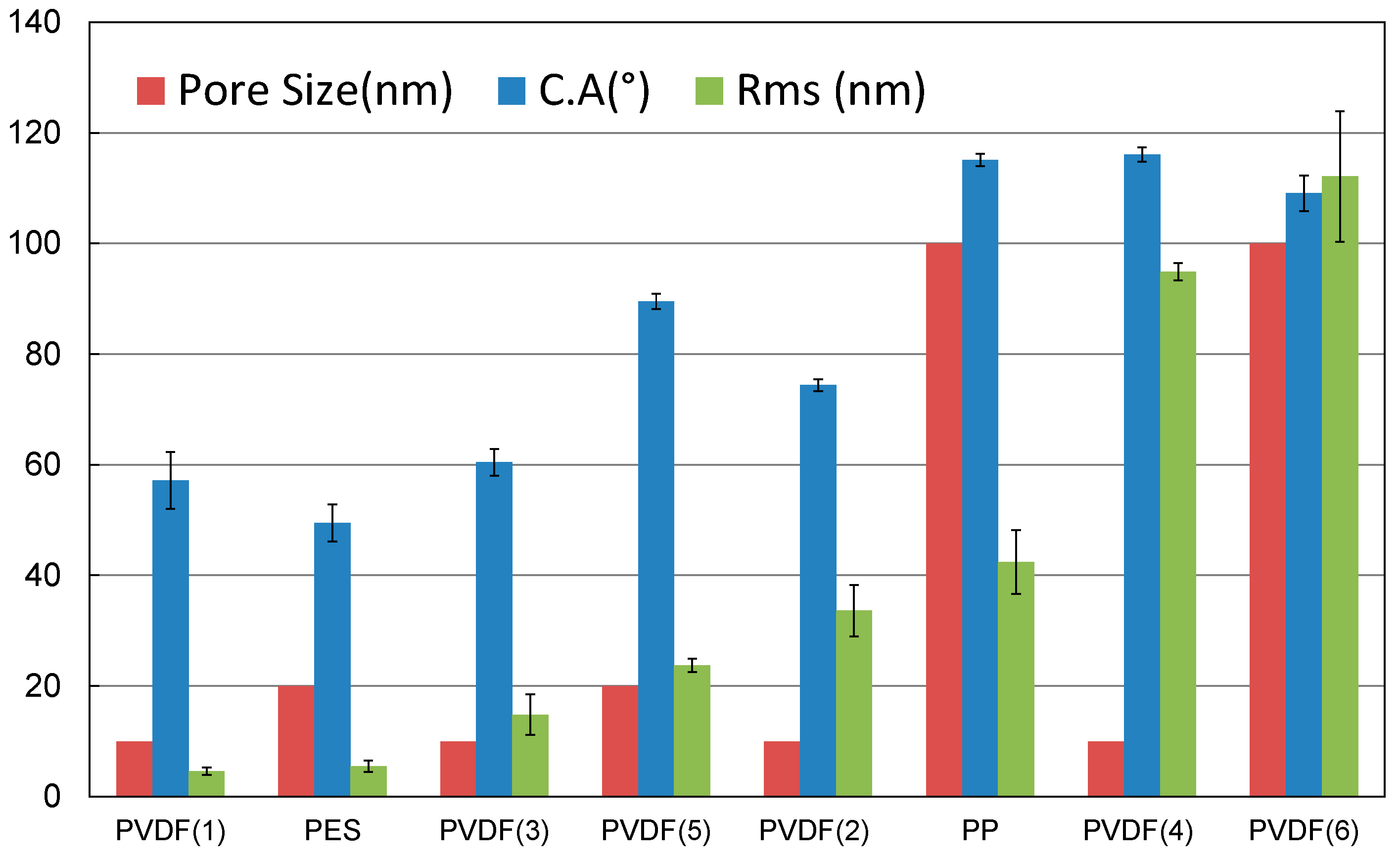
| No. | Substrate | Pore Size (nm) | CA (°) | RMS (nm) | CA/RMS | Graphene Transfer | Graphene Quality | Reason |
|---|---|---|---|---|---|---|---|---|
| 1 | PP | 100 | 115 ± 1.1 | 42.4 ± 5.8 | 2.7 | Yes | Good | Low roughness |
| 2 | PES | 20 | 50 ± 3.3 | 5.5 ± 1.0 | 9.2 | Failed | N/A | N/A |
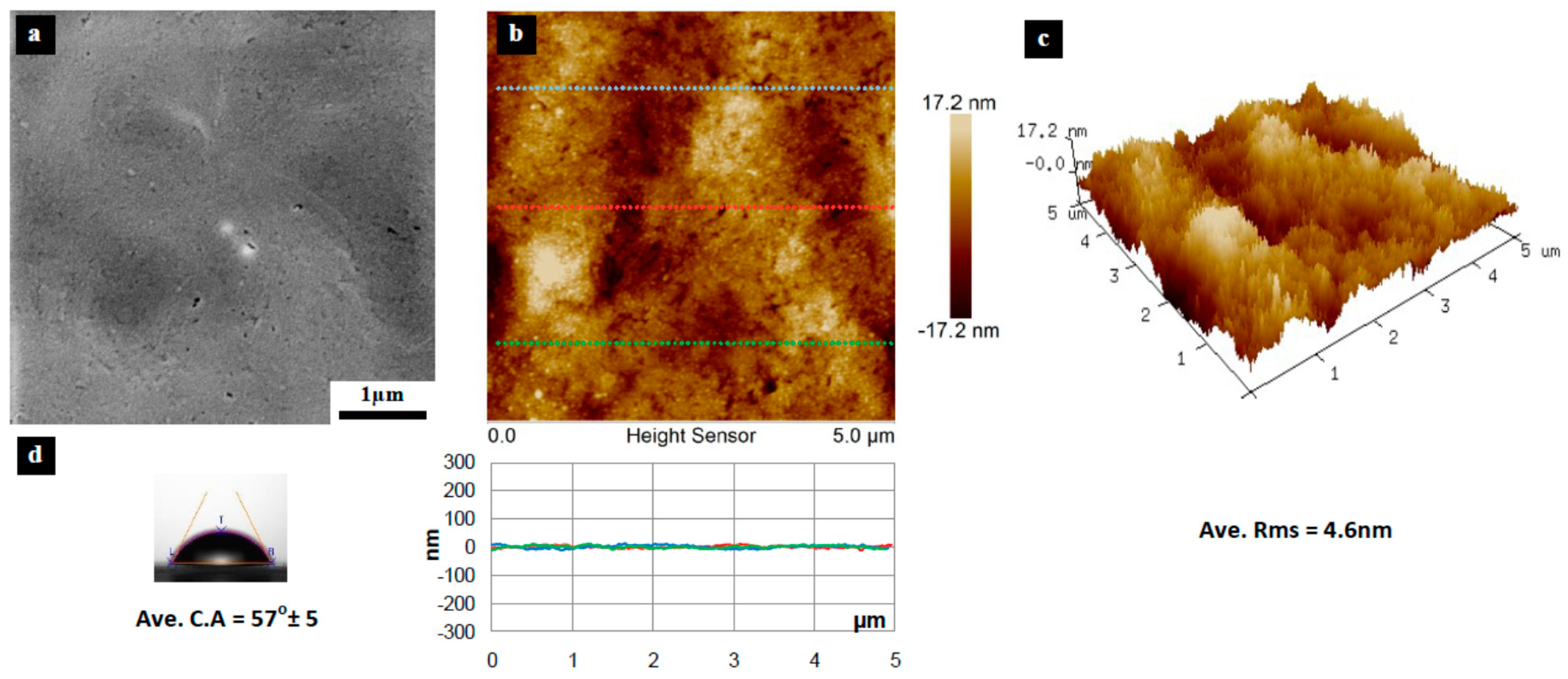
| 3 | PVDF 1 | 10 | 57 ± 5.1 | 4.6 ± 0.7 | 12.4 | Failed | N/A | N/A |
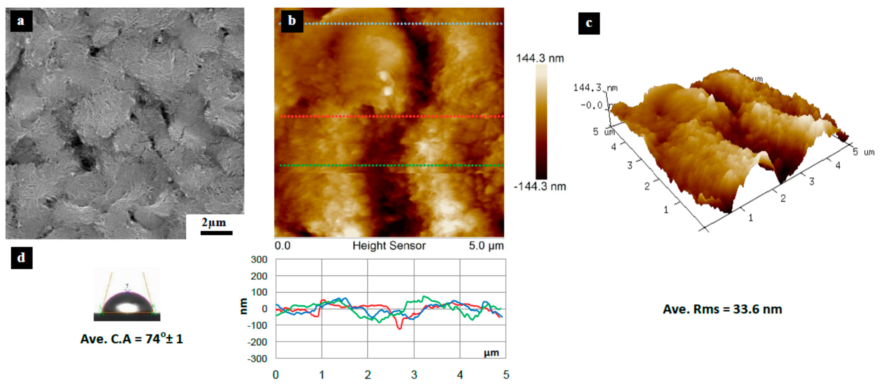
| 4 | PVDF 2 | 10 | 74 ± 1.1 | 33.6 ± 4.7 | 2.2 | Failed | N/A | N/A |
| 5 | PVDF 3 | 10 | 60 ± 2.4 | 14.8 ± 3.7 | 4.1 | Failed | N/A | N/A |
| 6 | PVDF 4 | 10 | 116 ± 1.3 | 94.9 ± 1.6 | 1.2 | Yes | Poor | High roughness |
| 7 | PVDF 5 | 20 | 90 ± 1.4 | 23.8 ± 1.2 | 3.8 | Yes | Good | Low roughness |
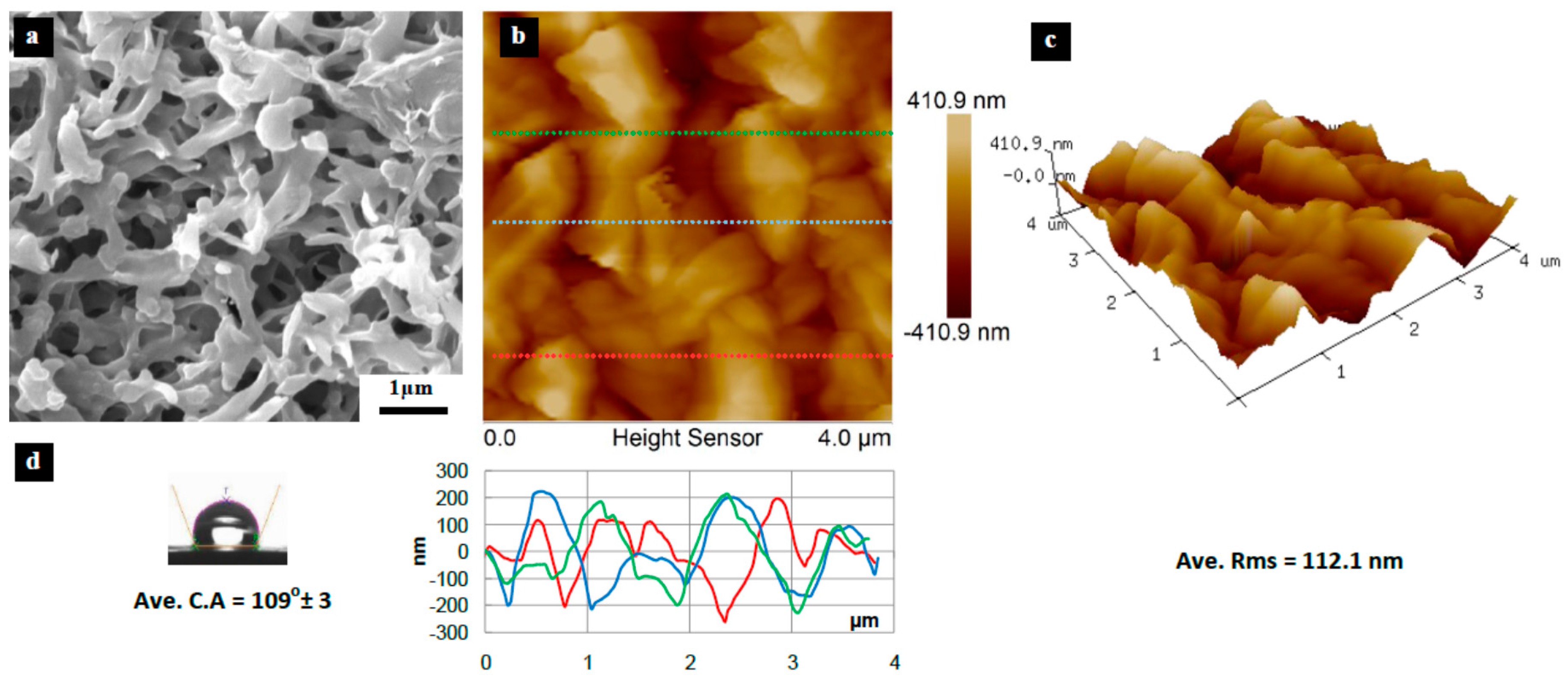
| 8 | PVDF 6 | 100 | 109 ± 3.2 | 112.1 ± 11.8 | 1.0 | Yes | Poor | High roughness |
© 2017 by the authors. Licensee MDPI, Basel, Switzerland. This article is an open access article distributed under the terms and conditions of the Creative Commons Attribution (CC BY) license ( http://creativecommons.org/licenses/by/4.0/).
Share and Cite
Kafiah, F.; Khan, Z.; Ibrahim, A.; Atieh, M.; Laoui, T. Synthesis of Graphene Based Membranes: Effect of Substrate Surface Properties on Monolayer Graphene Transfer. Materials 2017, 10, 86. https://doi.org/10.3390/ma10010086
Kafiah F, Khan Z, Ibrahim A, Atieh M, Laoui T. Synthesis of Graphene Based Membranes: Effect of Substrate Surface Properties on Monolayer Graphene Transfer. Materials. 2017; 10(1):86. https://doi.org/10.3390/ma10010086
Chicago/Turabian StyleKafiah, Feras, Zafarullah Khan, Ahmed Ibrahim, Muataz Atieh, and Tahar Laoui. 2017. "Synthesis of Graphene Based Membranes: Effect of Substrate Surface Properties on Monolayer Graphene Transfer" Materials 10, no. 1: 86. https://doi.org/10.3390/ma10010086