1. Introduction
There has been a long-standing research interest in surface acoustic wave (SAW) sensors for their wide applications in recent years [
1,
2,
3,
4]. Meanwhile, with the progress of science and technology, SAW sensors that operate stably in high temperatures are in high demand [
5]. As is widely known, the major challenge in fabricating SAW sensors for operating at high temperatures is to prepare film electrodes which can work stably at high temperatures. The main existing problem is that all the film electrodes undergo rapid agglomeration, recrystallization, and atom diffusion at temperatures higher than 700 °C, resulting in the destruction of film electrodes and the failure of SAW sensors. Until now, great efforts have been made to investigate the working of film electrodes at high temperatures. Moulzolf [
6,
7] co-deposited Pt/Rh (10%) as film electrodes and used HfO
2 as a passivation coating layer to hinder the agglomeration. Taguetta [
8] used Ir-Rh alloy electrodes of different compositions and found that Ir-based film electrodes can withstand temperatures as high as 800 °C. Rane [
9,
10] used tungsten film electrodes to prevent the diffusion of Ga and O atoms from the substrate and obtained stable sensors up to 800 °C. Pereira da Cunha [
11] investigated a Pt-Ni/Pt-Zr electrode containing an Al
2O
3 interfacial layer that was used to reduce the degradation of the electrode layer by inhibiting the interdiffusion and interfacial reactions. In our previous work [
12], we prepared a AlN/Pt/ZnO multilayered electrode on Langasite (LGS, La
3Ga
5SiO
14) substrate and found that the ZnO buffer layer improved the crystalline quality of Pt by inhibiting the recrystallization of Pt film at 1000 °C, showing that the crystalline quality is an important factor in determining the stability of film electrodes at high temperature. However, the abovementioned AlN/Pt/ZnO film electrode was unable to work steadily above 1100 °C because both agglomeration and the interdiffusion (of the Ga, Si, and La atoms) were difficult to control at such high temperatures.
According to previous reports, we can find that the agglomeration in metal electrodes and the interdiffusion always occur at high temperatures. It is therefore necessary to find a barrier layer to prevent the interdiffusion from substrate to the film electrode. In this work, we inserted an Al2O3 film as a barrier layer between LGS substrate and ZnO buffer layer to prevent the interfacial diffusion. The Al2O3/Pt/ZnO/Al2O3 electrode was then fabricated on LGS to explore its characteristic, from room temperature to 1200 °C.
2. Results and Discussion
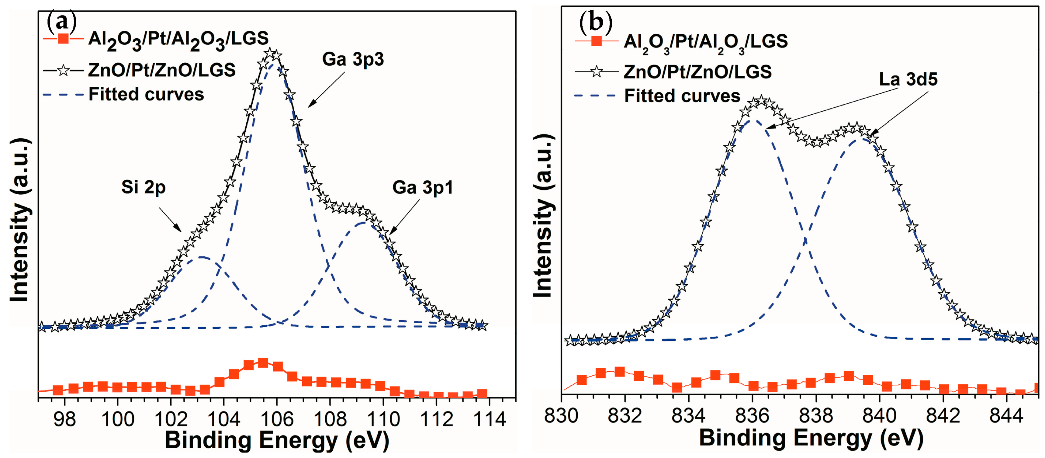
Figure 1 shows the X-ray photoelectron spectroscopy (XPS) spectra of ZnO(160 nm)/Pt(30 nm)/ZnO(60 nm)/LGS and Al
2O
3(160 nm)/Pt(30 nm)/Al
2O
3(60 nm)/LGS samples after annealing at 1000 °C for 1 h. In
Figure 1a, the Ga 3p and Si 2p peaks of the two samples after annealing at 1000 °C are presented. It can be seen that the intensities of the Ga 3p and Si 2p peaks of Al
2O
3/Pt/Al
2O
3/LGS sample are much lower than those of ZnO/Pt/ZnO/LGS sample. Similarly, from
Figure 1b, we can see that the La 3d5 peaks of Al
2O
3/Pt/Al
2O
3/LGS sample are so low that it can barely be observed. On the other hand, the XPS spectrum of ZnO/Pt/ZnO/LGS sample shows obvious La 3d5 peaks. These results reveal the greater presence of Ga, Si, and La atoms at the surface of ZnO/Pt/ZnO/LGS sample compared to Al
2O
3/Pt/Al
2O
3/LGS sample. Therefore, it can be concluded that the Al
2O
3 layer can prevent the diffusion of the Ga, Si, and La atoms from the LGS substrate to film electrode and the ZnO layer cannot prevent the atoms’ diffusion. The reduction of the diffusion in Al
2O
3/Pt/Al
2O
3/LGS sample was attributed to the higher chemical stability of Al
2O
3 [
13,
14,
15]. Until now, the Al
2O
3/Pt-Ni/Al
2O
3 film electrode [
11] has demonstrated that the Al
2O
3 film can be used as a suitable diffusion barrier layer for LGS substrate. It was the reason why we focus on the film electrode by using Al
2O
3 barrier layer next.
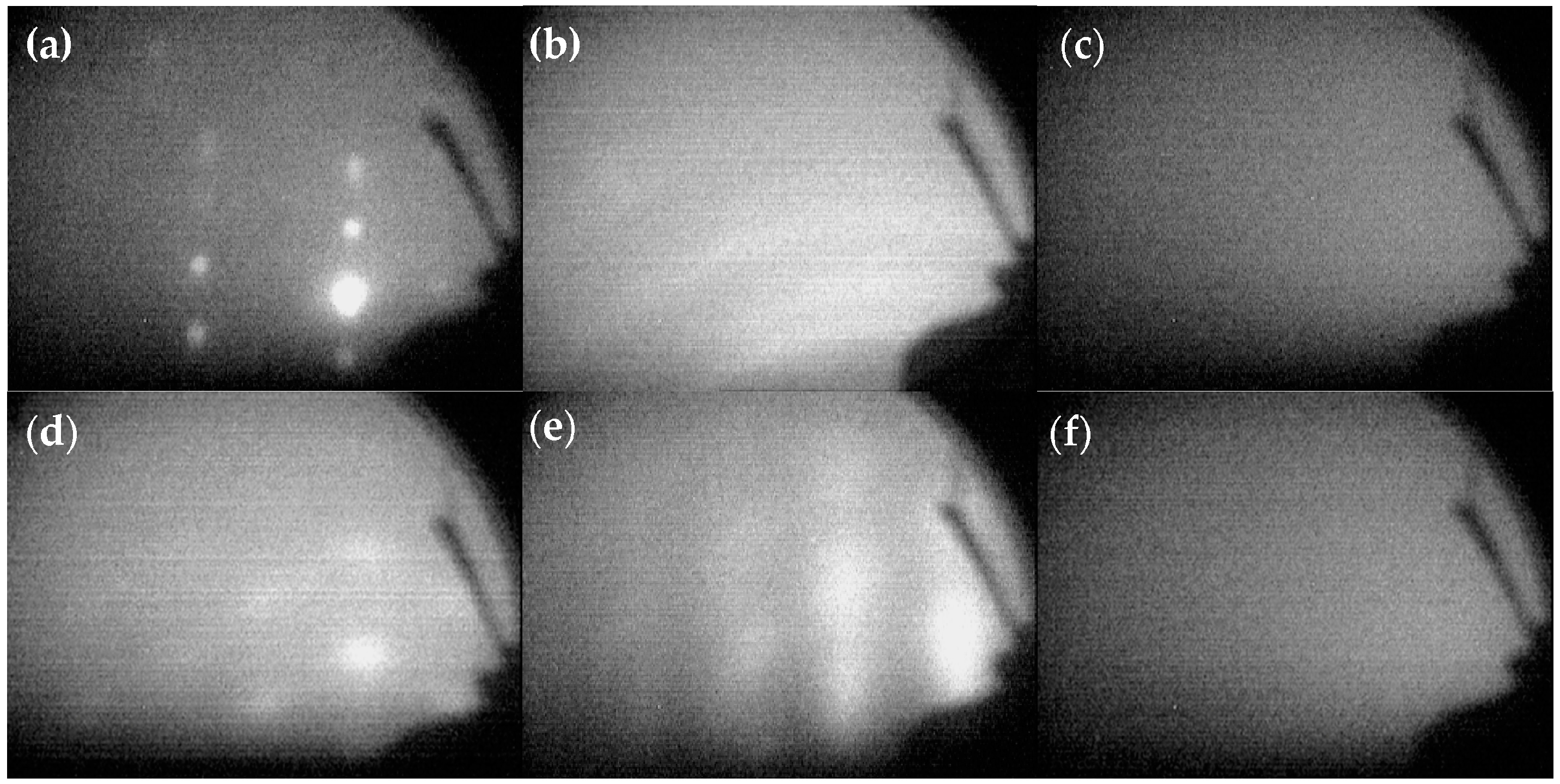
The reflected high energy electron diffraction (RHEED) patterns obtained during the deposition of Al
2O
3/Pt/ZnO/Al
2O
3 are shown in
Figure 2.
Figure 2a shows the bright diffraction spots of LGS that indicate that its surface was cleaned well.
Figure 2b shows the RHEED pattern of ZnO directly deposited on LGS at 150 °C. The obvious diffraction rings indicate that the ZnO crystals were uniaxially textured, with the preferred orientation being out-of-plane. It shows that the ZnO deposited on LGS directly did not have sufficient crystalline quality. No diffraction spots were observed in
Figure 2c, suggesting that the Al
2O
3 barrier layer either was not preferentially oriented or remained amorphous due to a low deposition temperature and the complete mismatch in the lattice structures of Al
2O
3 and LGS. However, as shown in
Figure 2d, the RHEED pattern of the ZnO film deposited on an Al
2O
3 barrier layer shows bright diffraction spots that indicate the ZnO film was biaxially textured, with both the out-of-plane and in-plane preferred orientations. Thus, the deposition of ZnO on an Al
2O
3 barrier layer resulted in a better crystalline quality compared to that for a ZnO film deposited on LGS directly. In this study, we deposited 10 nm of ZnO and the ZnO buffer layer was kept so thin to reduce the influence of their mass effects on the properties of SAW devices. The Pt film deposited on the ZnO buffer layer also revealed bright diffraction spots, as shown in
Figure 2e, indicating the good crystalline quality of the as-deposited Pt. Finally, the Al
2O
3 deposited as a protective layer was amorphous, as can be inferred from the absence of diffraction spots in
Figure 2f.
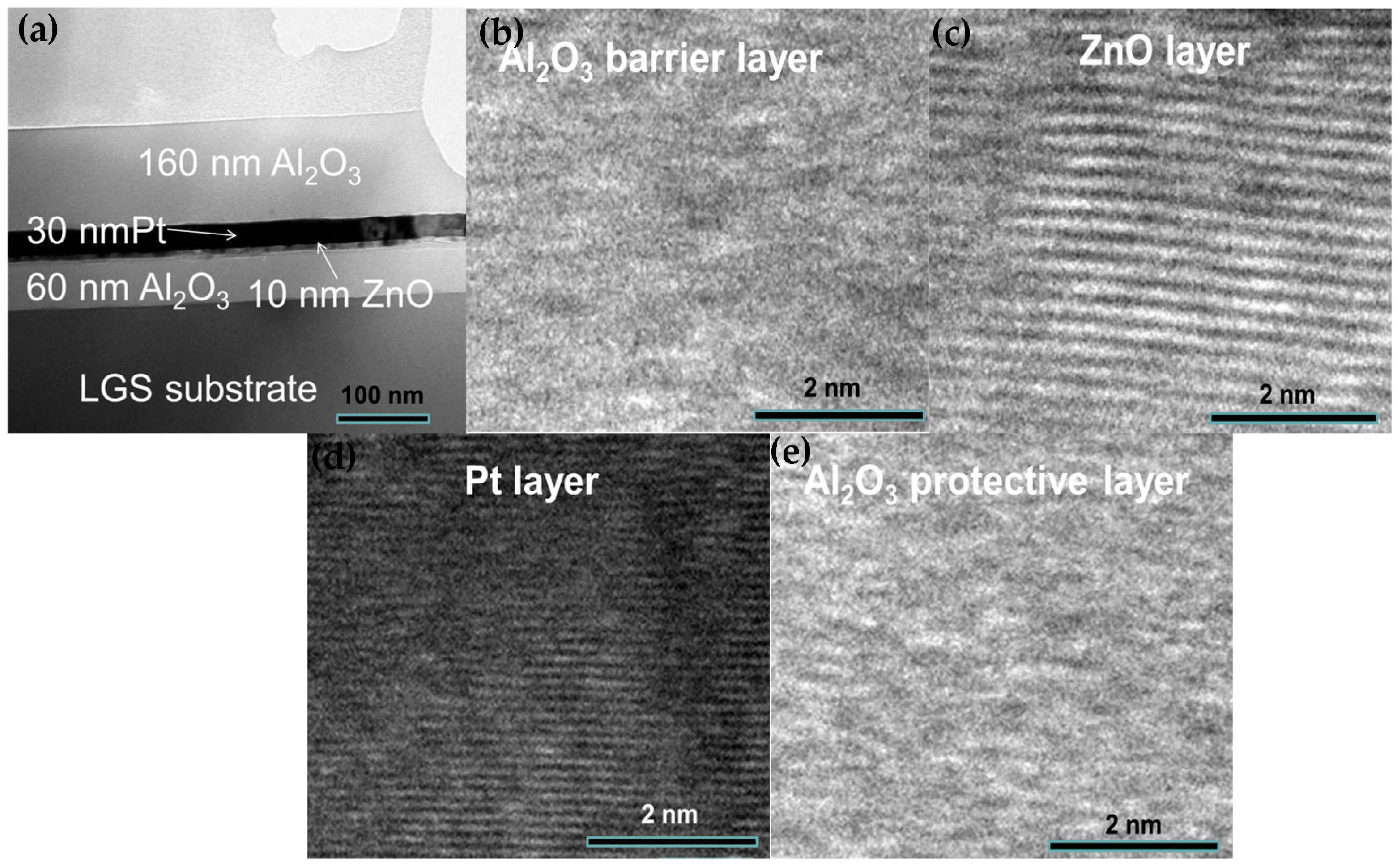
Figure 3a shows the cross-sectional TEM (transmission electron microscope) image of Al
2O
3/Pt/ZnO/Al
2O
3/LGS heterostructure. We can see the clear interfaces.
Figure 3b–e show the enlarged cross-sectional high resolution TEM image of Al
2O
3 barrier layer, ZnO buffer layer, Pt layer, and Al
2O
3 protective layer, respectively. From these figures, we can determine that the Al
2O
3 layers are both in amorphous states and the ZnO, Pt films have preferred orientations. These results are consistent with the RHEED patterns as shown in
Figure 2.
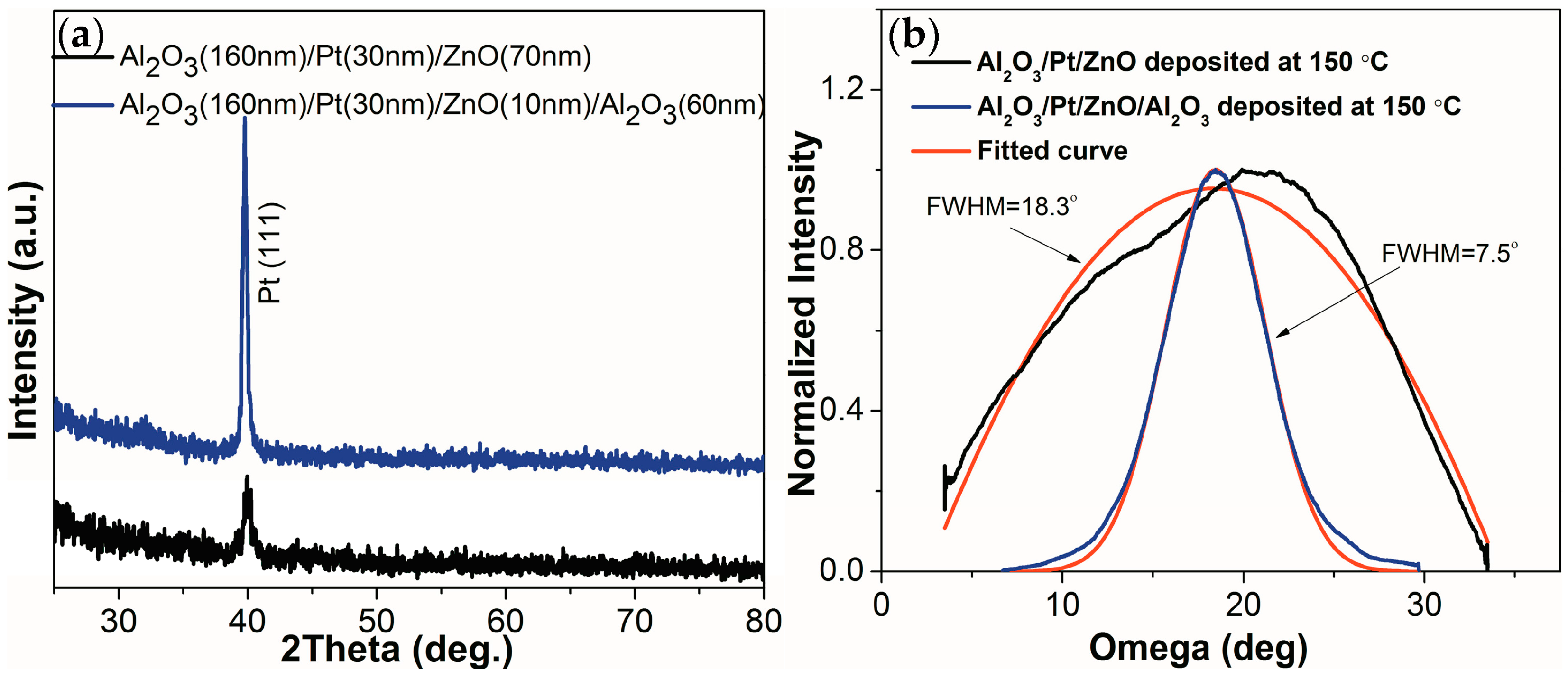
Figure 4 shows the θ–2θ and omega XRD (X-ray diffraction) scans of the Al
2O
3/Pt/ZnO/LGS and Al
2O
3/Pt/ZnO/Al
2O
3/LGS samples. From
Figure 4a, we can see that only the Pt (111) peaks appear in these two samples. No ZnO peaks can be observed in these patterns because this this ZnO film was too thin to be detected [
12]. The intensity of the Pt (111) peak is much lower for Al
2O
3/Pt/ZnO/LGS than Al
2O
3/Pt/ZnO/Al
2O
3/LGS. The full width at half maximum (FWHM) of these two peaks are shown in
Figure 4b, and were determined to be 7.5° and 18.3° for Al
2O
3/Pt/ZnO/Al
2O
3/LGS and Al
2O
3/Pt/ZnO/LGS respectively. These results show that the crystalline quality of the Pt (111) layer was greatly improved by inserting the Al
2O
3 barrier layer. The large FWHM of the Pt peak of Al
2O
3/Pt/ZnO/LGS is due to the low temperature of deposition of the ZnO buffer layer, which results in the poor crystalline qualities of both ZnO and Pt. The crystalline qualities these films are typically improved by increasing the deposition temperature to 600 °C [
12]. However, we have found that by inserting an Al
2O
3 barrier layer we can improve the crystalline quality of the ZnO buffer layer deposited at low temperatures; this was possible because of their similar crystal structures [
16,
17]. Thus, a Pt film of good crystalline quality could be deposited on an improved ZnO buffer layer at relatively lower temperatures. The low deposition temperature of 150 °C is very important for fabricating patterned film electrodes using lithography and the subsequent lift-off process.
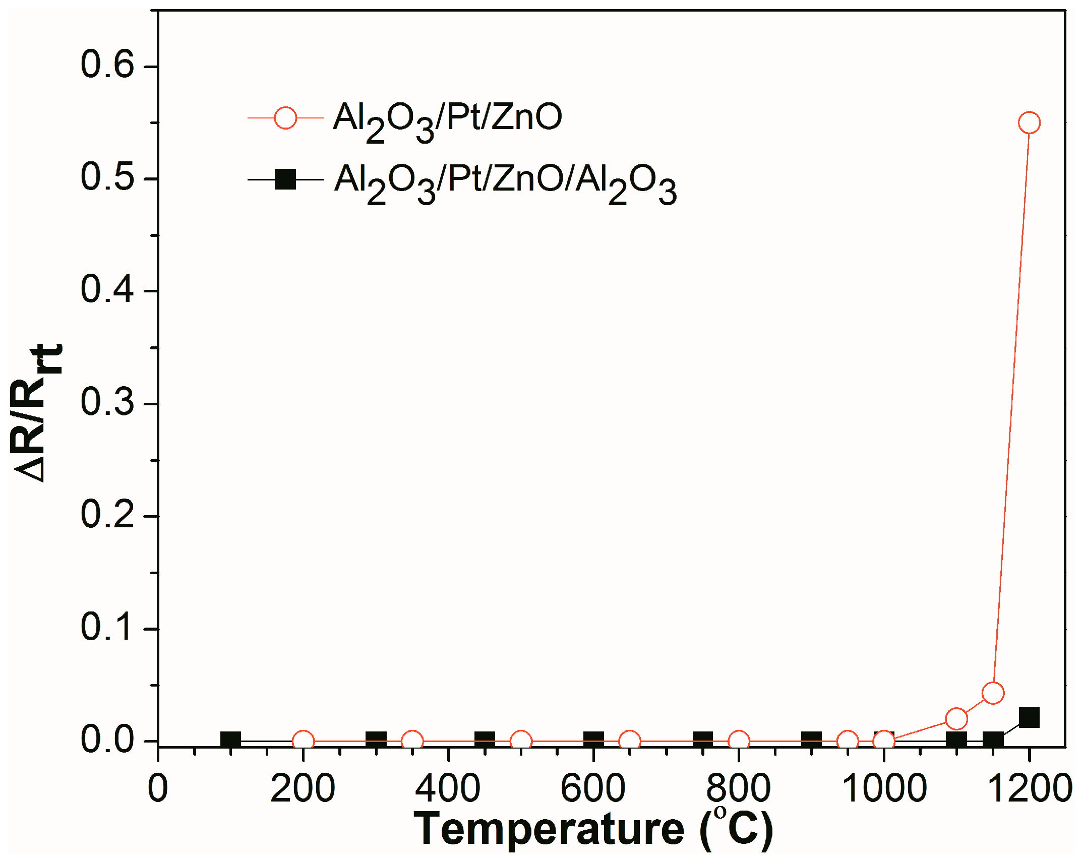
Figure 5 shows the real-time, relative resistance change (ΔR/R
rt) as a function of temperature for Al
2O
3/Pt/ZnO/Al
2O
3/LGS and Al
2O
3/Pt/ZnO/LGS samples, where R
rt is the resistance of the sample at room temperature and ΔR is the difference between the resistances at high temperature and room temperature. It can be seen that the resistance of the Al
2O
3/Pt/ZnO/LGS sample does not vary from room temperature to 1000 °C and increases slowly from 1000 °C to 1150 °C. From 1150 °C to 1200 °C, the resistance increases sharply. Finally, the resistance increases by 0.55 times, from room temperature to 1200 °C. For the Al
2O
3/Pt/ZnO/Al
2O
3/LGS sample, the resistance does not vary from room temperature to 1150 °C and increases by only 0.02 times from 1150 °C to 1200 °C. These results show that the stability of Al
2O
3/Pt/ZnO/Al
2O
3/LGS electrode at high temperature has been improved greatly by the Al
2O
3 barrier layer.
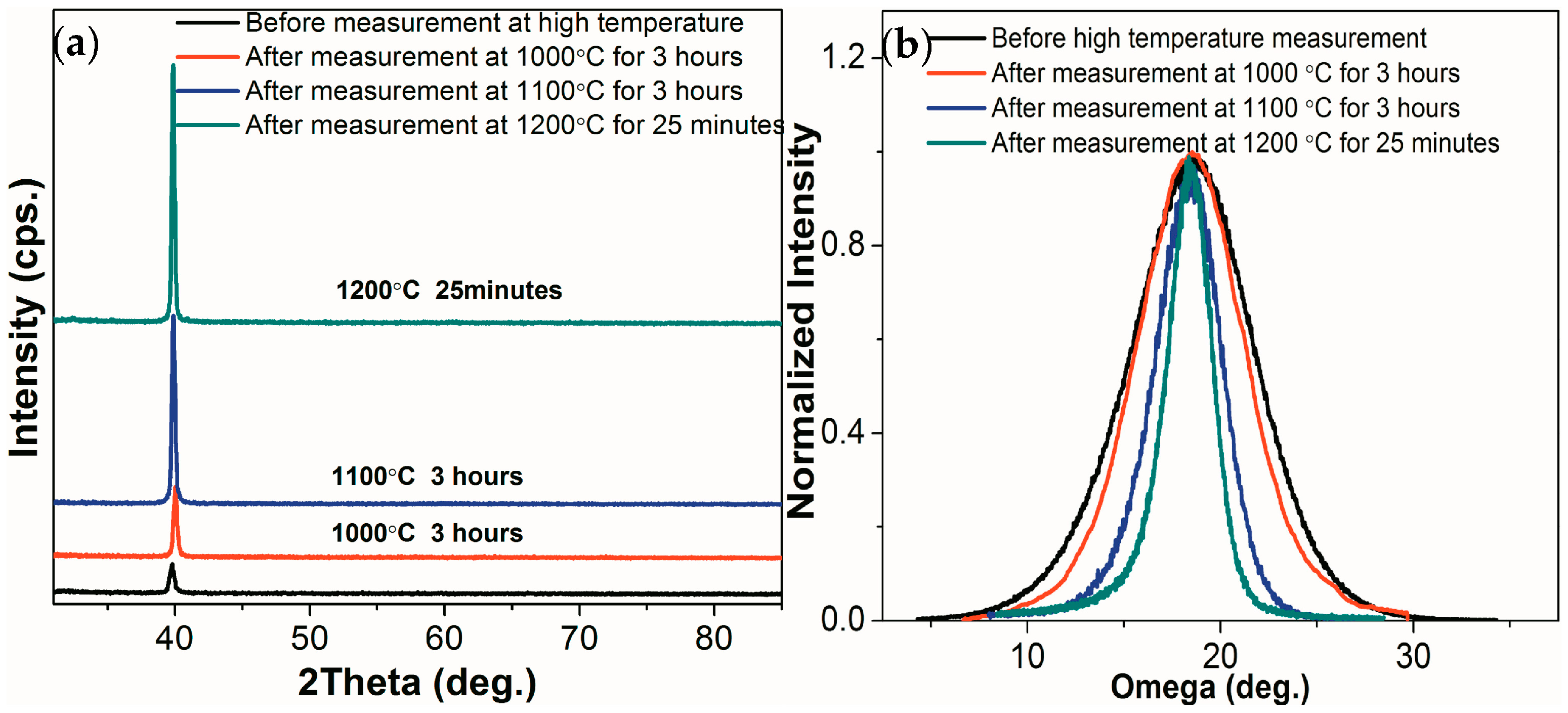
Figure 6 shows the θ–2θ scans and omega scans of the Al
2O
3/Pt/ZnO/Al
2O
3/LGS samples before and after resistance measurement at 1000, 1100, and 1200 °C. As shown in
Figure 6a, the intensity of Pt (111) peak doubled after the high temperature measurement at 1000 °C for 3 h. Besides, the FWHM of Pt (111) peak decreased from 7.5° to 6.8° as shown in
Figure 6b after resistance measurement at 1000 °C for 3 h. Both the intensity and FWHM of the Pt (111) peaks varied by only a little after resistance measurement at 1000 °C for 3 h, showing that the recrystallization of Pt film was hindered well at 1000 °C. While, after resistance measurement at 1100 °C for 3 h and at 1200 °C for 25 min, the intensity of Pt (111) peak increased by 7 times and 10.6 times. Meanwhile, the FWHM of Pt (111) peak varied from 7.5° to 3.8° and 2.5° respectively, which indicates that the recrystallization of Pt film occurs partly at 1100 °C and the recrystallization cannot be prevented totally at 1200 °C.
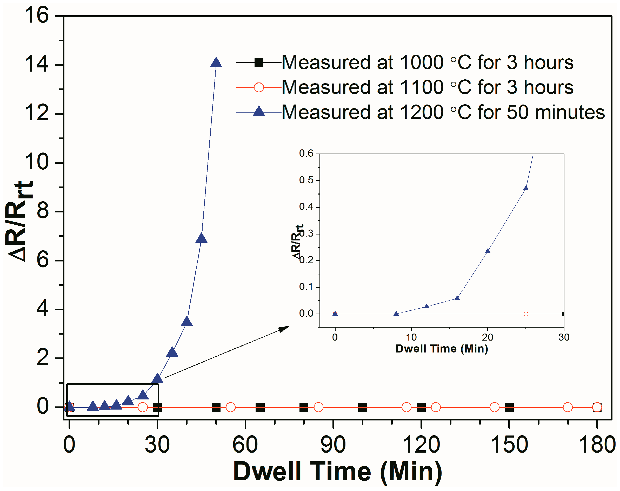
Figure 7 shows the real-time relative resistance measurement of Al
2O
3/Pt/ZnO/Al
2O
3/LGS samples at 1000 °C and 1100 °C for 3 h, and at 1200 °C for 50 min. After undergoing resistance measurement at high temperature of 1000 °C or 1100 °C for 3 h, the samples remain the same resistance all the time, indicating that the Al
2O
3/Pt/ZnO/Al
2O
3/LGS electrode can work stably at 1100 °C for 3 h. For Al
2O
3/Pt/ZnO/Al
2O
3/LGS sample measured at 1200 °C, the resistance increases slowly before 25 min and increases rapidly after 25 min. The resistance increases to infinity in 55 min. It shows that this electrode can work at 1200 °C only in a short period of time. Compared to other reported multilayer electrodes such as Pt-Rh/HfO
2 [
6] and Al
2O
3/Pt-Ni/Al
2O
3 [
11], the stability of this Al
2O
3/Pt/ZnO/Al
2O
3/LGS electrode at high temperature has been improved greatly.
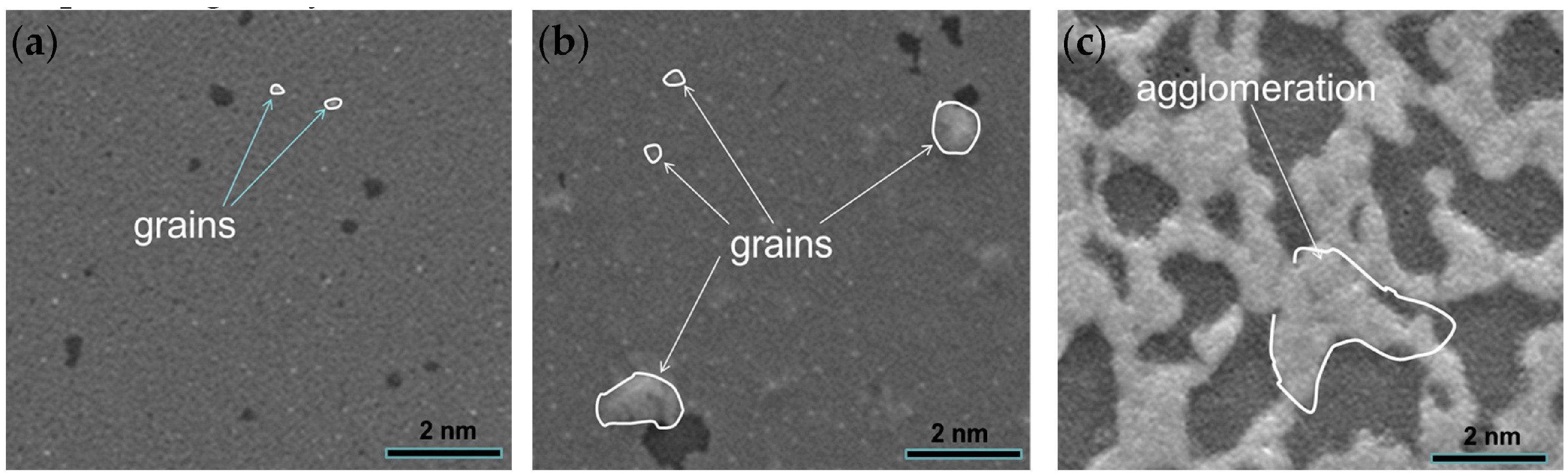
Figure 8 shows the surface topography of Al
2O
3/Pt/ZnO/Al
2O
3/LGS samples after high temperature resistance measurements at 1000, 1100, and 1200 °C, respectively. From
Figure 8, we can see that the surface is smooth with few and small grains (marked out by curves) after resistance measurements at 1000 °C for 3 h, indicating that the film agglomerated slightly.
Figure 8b shows the surface topography of Al
2O
3/Pt/ZnO/Al
2O
3/LGS sample after resistance measurement at 1100 °C for 3 h. The surface was still smooth but we can observe more and bigger grains. It shows that more severe agglomerations occurred after 1100 °C resistance measurement. However, these agglomerations are both not sufficient to increase the film resistance greatly as shown in
Figure 7. Finally, it can be seen from
Figure 8c that much more severe agglomeration occurred after the resistance measurement at 1200 °C for 25 min, which is similar to other film electrodes after high temperature measurements [
18,
19,
20].
3. Materials and Methods
The Al2O3/Pt/ZnO/Al2O3 multilayer electrodes were grown by LMBE on LGS substrates with Euler angle of (0°, 138.5°, 116.6°) at 150 °C. A KrF (λ = 248 nm) excimer laser was operated with an energy density of about 2.5 J/cm2 at a frequency of 3 Hz. Highly purified Al2O3, Pt, and ZnO targets were used in this work and the distance from target to substrate was kept at 6 cm. Before depositing, the LGS substrates were ultrasonically cleaned in anhydrous alcohol for 6 min, followed by a N2 drying process. Then, the substrate was loaded into the deposition chamber and heated up to 150 °C. The chamber pressure was maintained at 3 × 10⁻⁵ Pa during growth. Finally, a 60 nm Al2O3 barrier layer, 10 nm ZnO buffer layer, and 30 nm Pt and 160 nm Al2O3 protective layer were deposited on LGS one by one. In addition, ZnO(160 nm)/Pt(30 nm)/ZnO(70 nm), Al2O3 (160 nm)/Pt(30 nm)/Al2O3(70 nm), and Al2O3(160 nm)/Pt(30 nm)/ZnO(70 nm) electrodes were also fabricated at 150 °C to study their diffusion and conductive properties at high temperature.
The growth patterns of all films were monitored by in situ RHEED diagnostic using a 20 kV electron beam. The resistances of the samples were measured from room temperature to 1200 °C in air within a tube furnace by a resistance meter (Keithley 2400, Tektronix, Cleveland, OH, USA). The heating rate was kept as 4 °C per minute. After high temperature resistance measurement, the samples were cooling down to room temperature in a natural cooling condition. Film crystal structure and texture were measured by X-ray diffraction (XRD) (D1System, Bede, Durham, UK) and transmission electron microscope (TEM) (Tecnai G2 F20, FEI, Hillsboro, OR, USA). A scanning electron microscope (SEM) (JSM-7500F, JEOL, Tokyo, Japan) was used to characterize the surface topography of the samples before and after high temperature resistance measurement. The component of each atom was characterized by the X-ray photoelectron spectroscopy (XPS) (AXIS Ultra DLD, Kratos, Manchester, UK).
