Mutual Effects of Fluorine Dopant and Oxygen Vacancies on Structural and Luminescence Characteristics of F Doped SnO2 Nanoparticles

Abstract
:
1. Introduction
2. Experimental
3. Results and Discussion
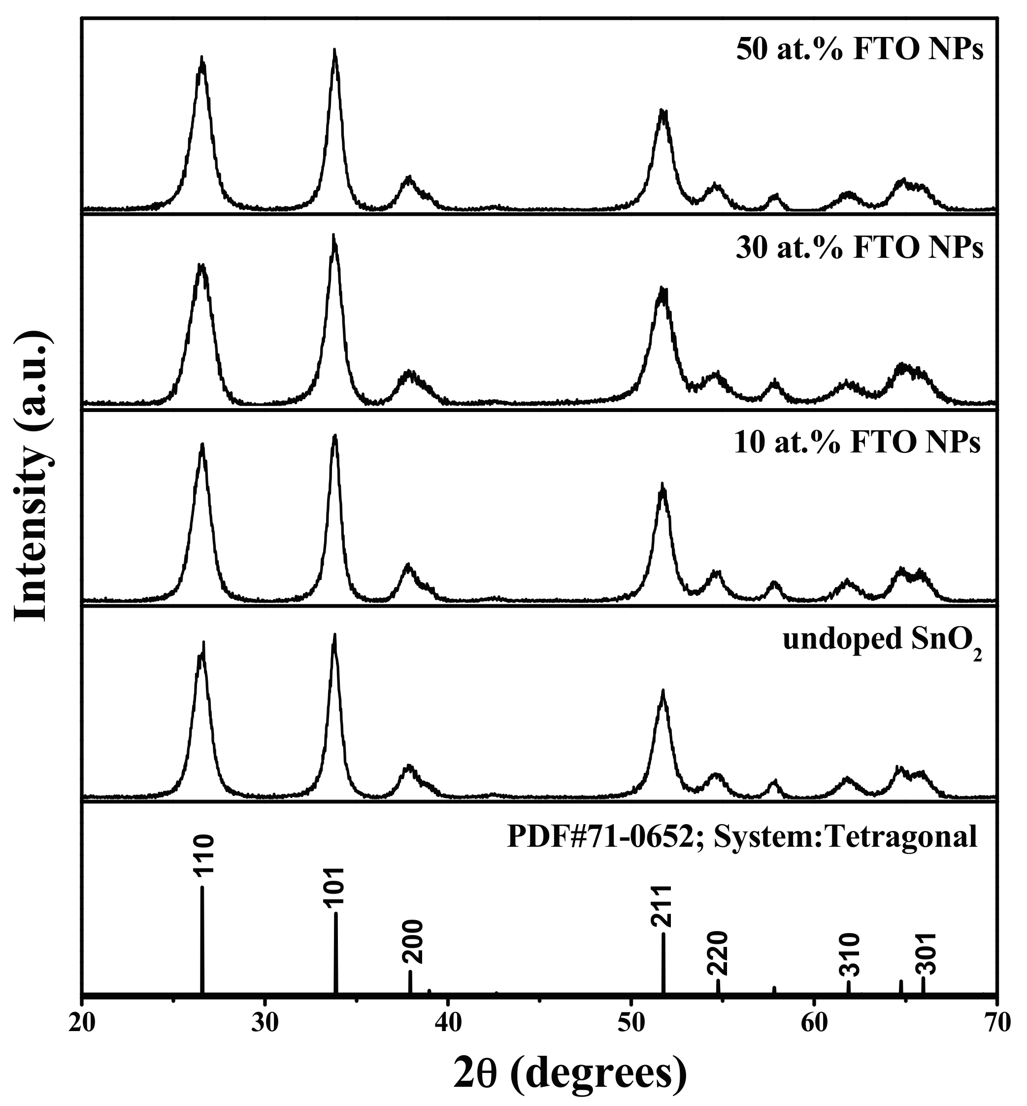
3.1. XRD Analysis
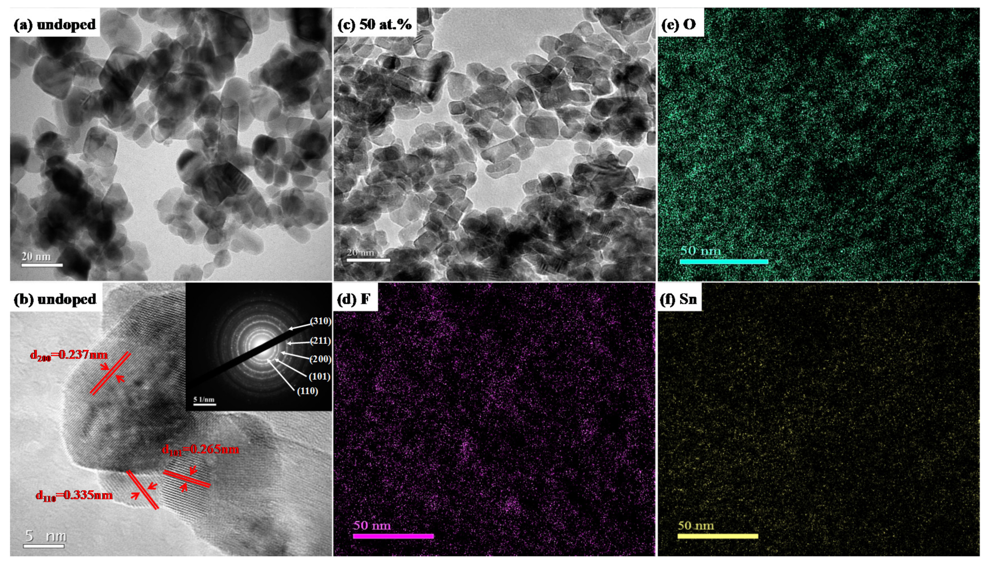
3.2. TEM Analysis
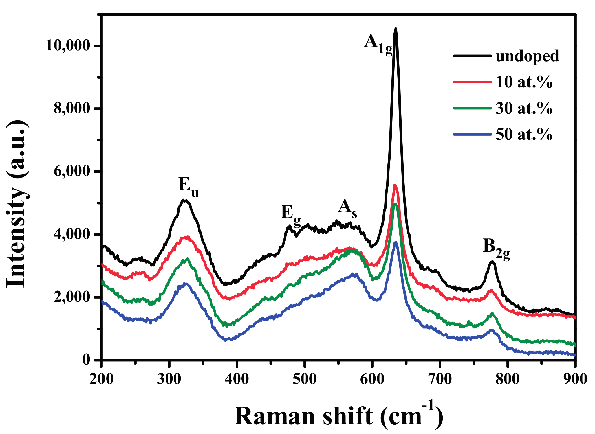
3.3. Raman Spectra Analysis
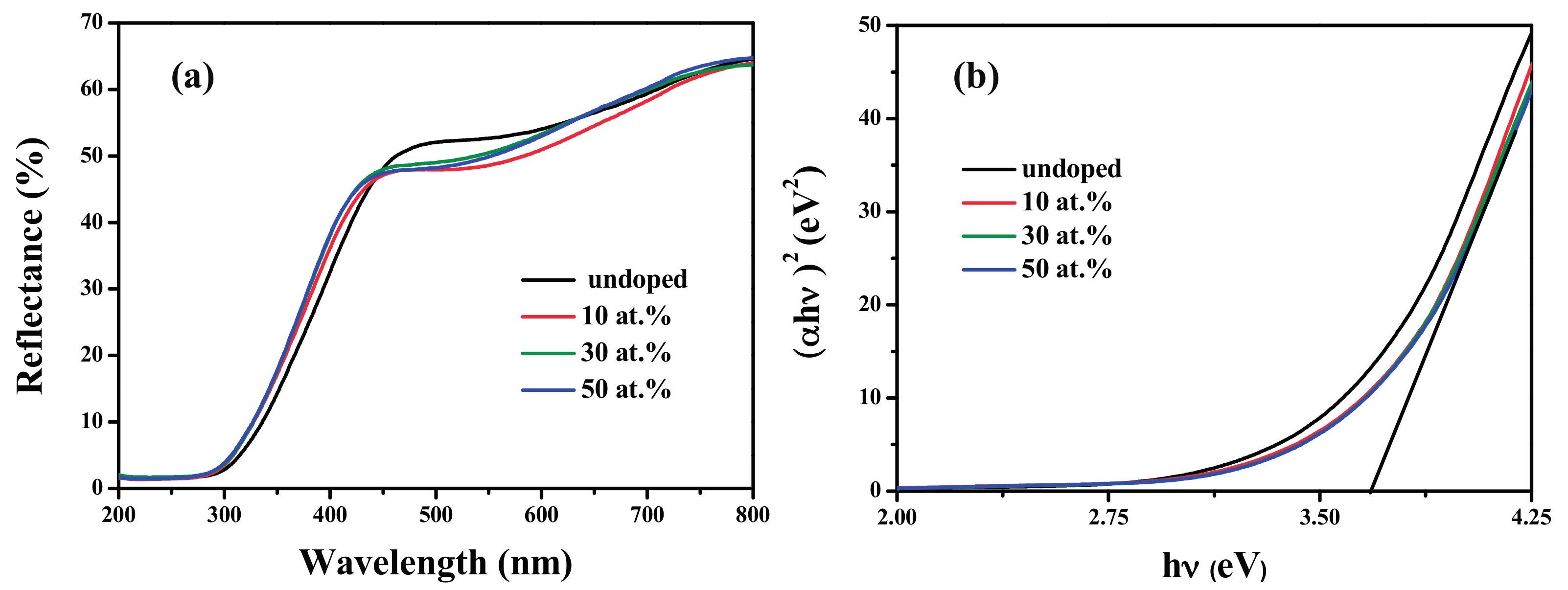
3.4. Optical Properties
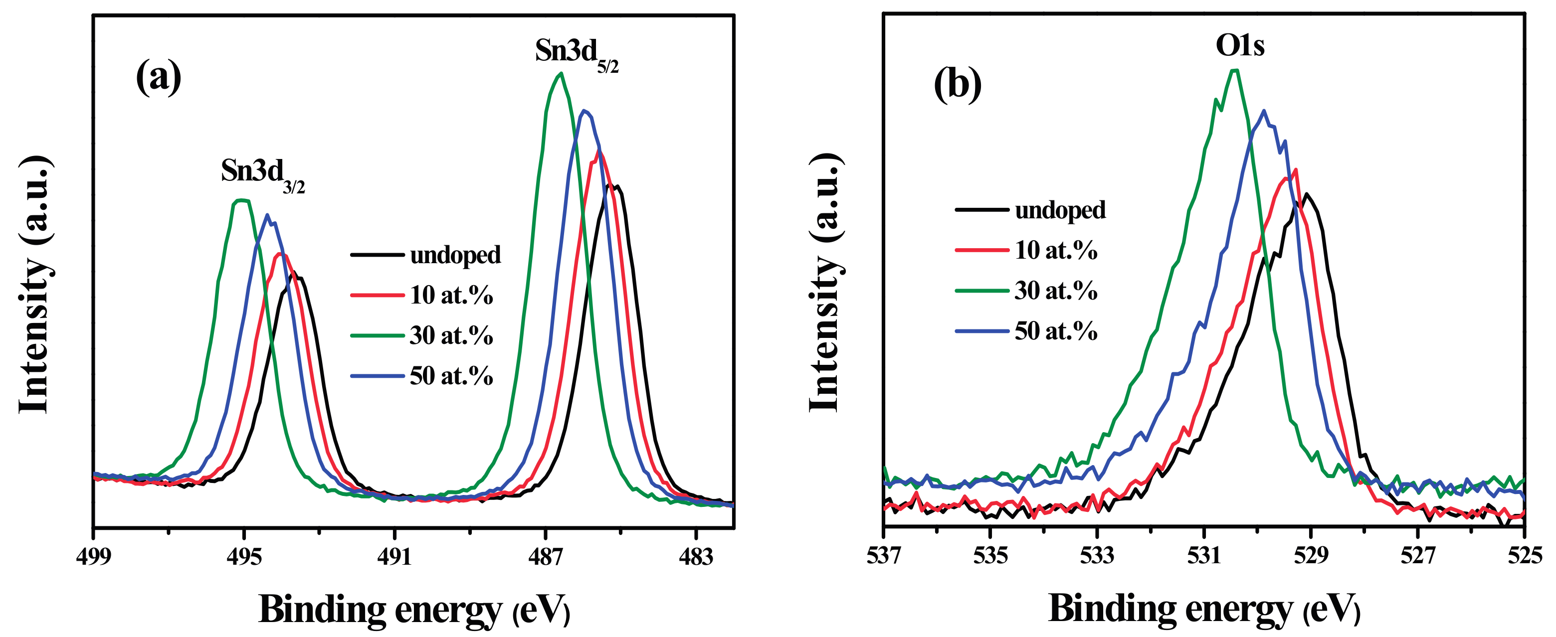
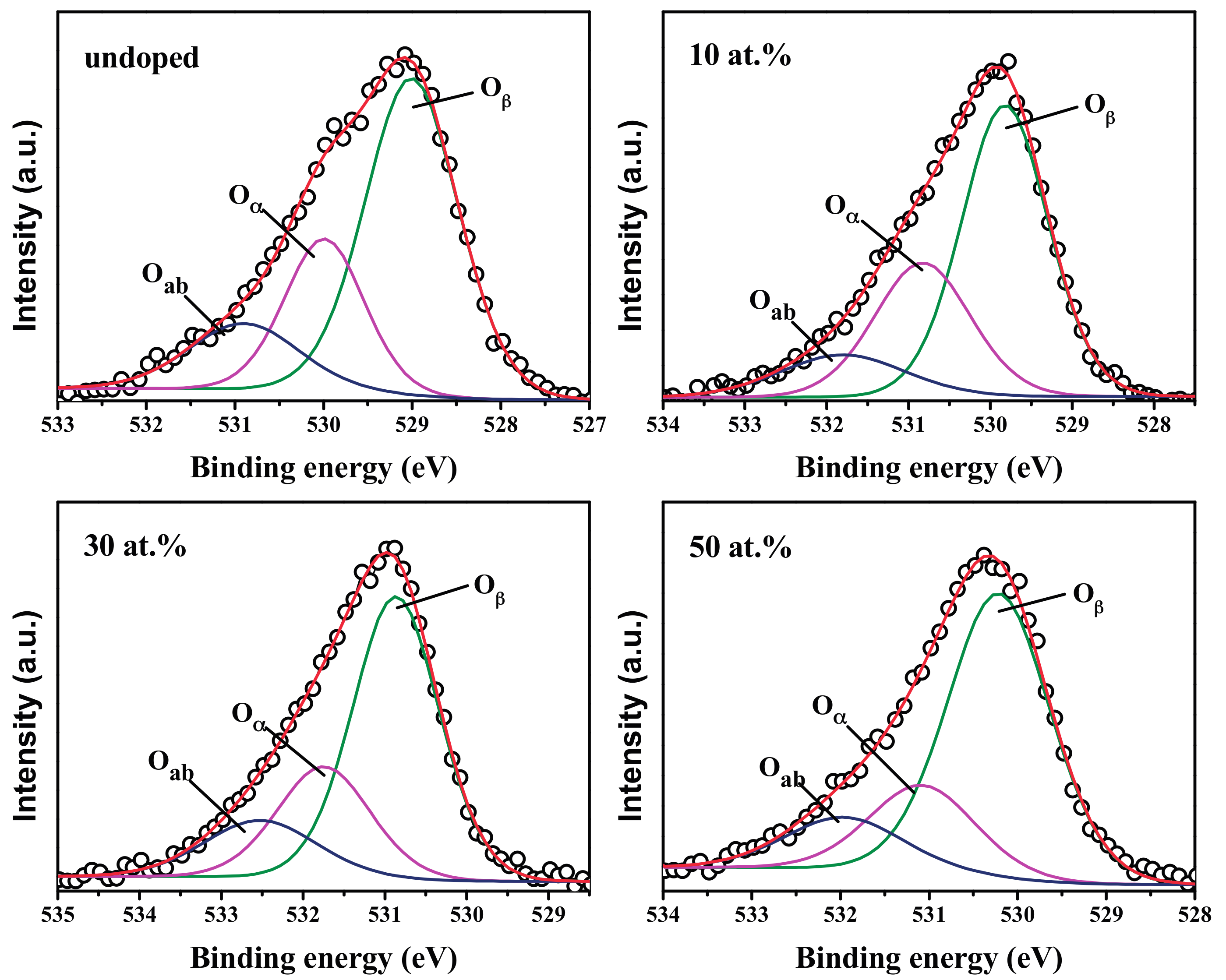
3.5. XPS Analysis
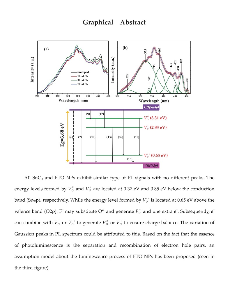
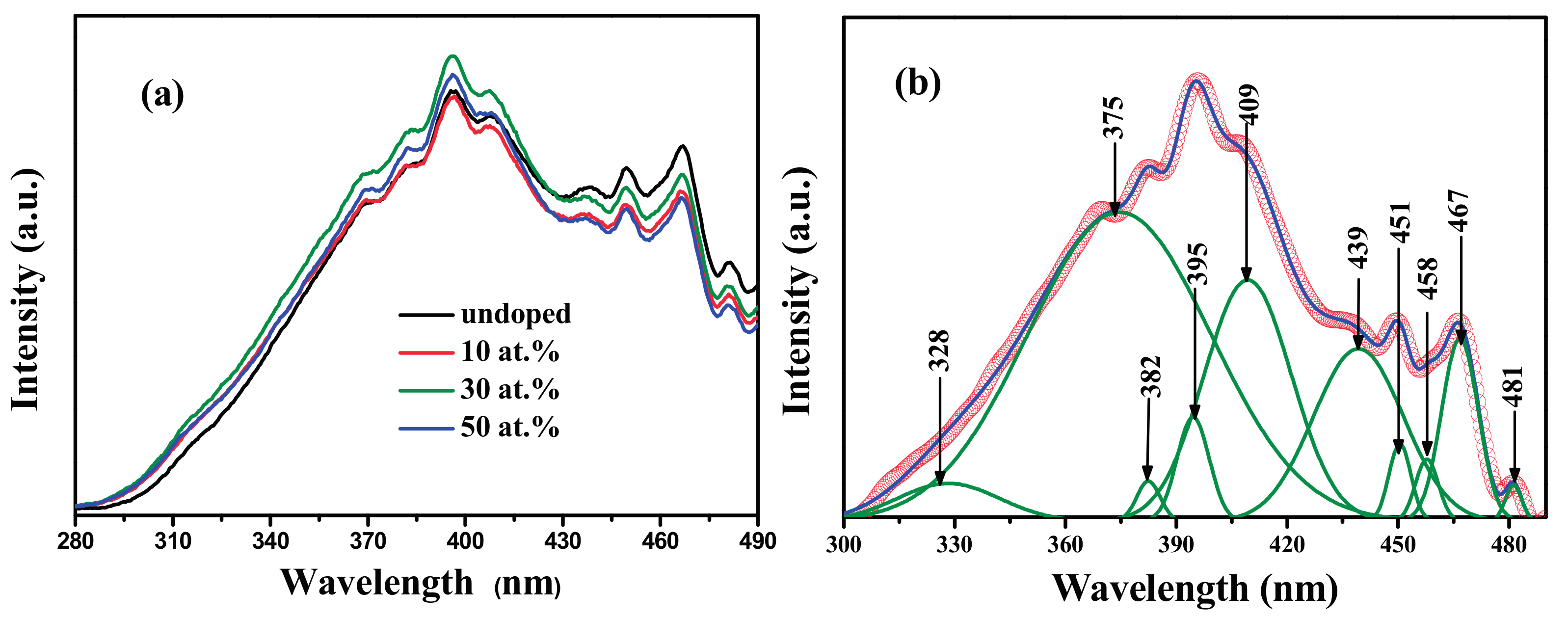
3.6. Photoluminescence Performance
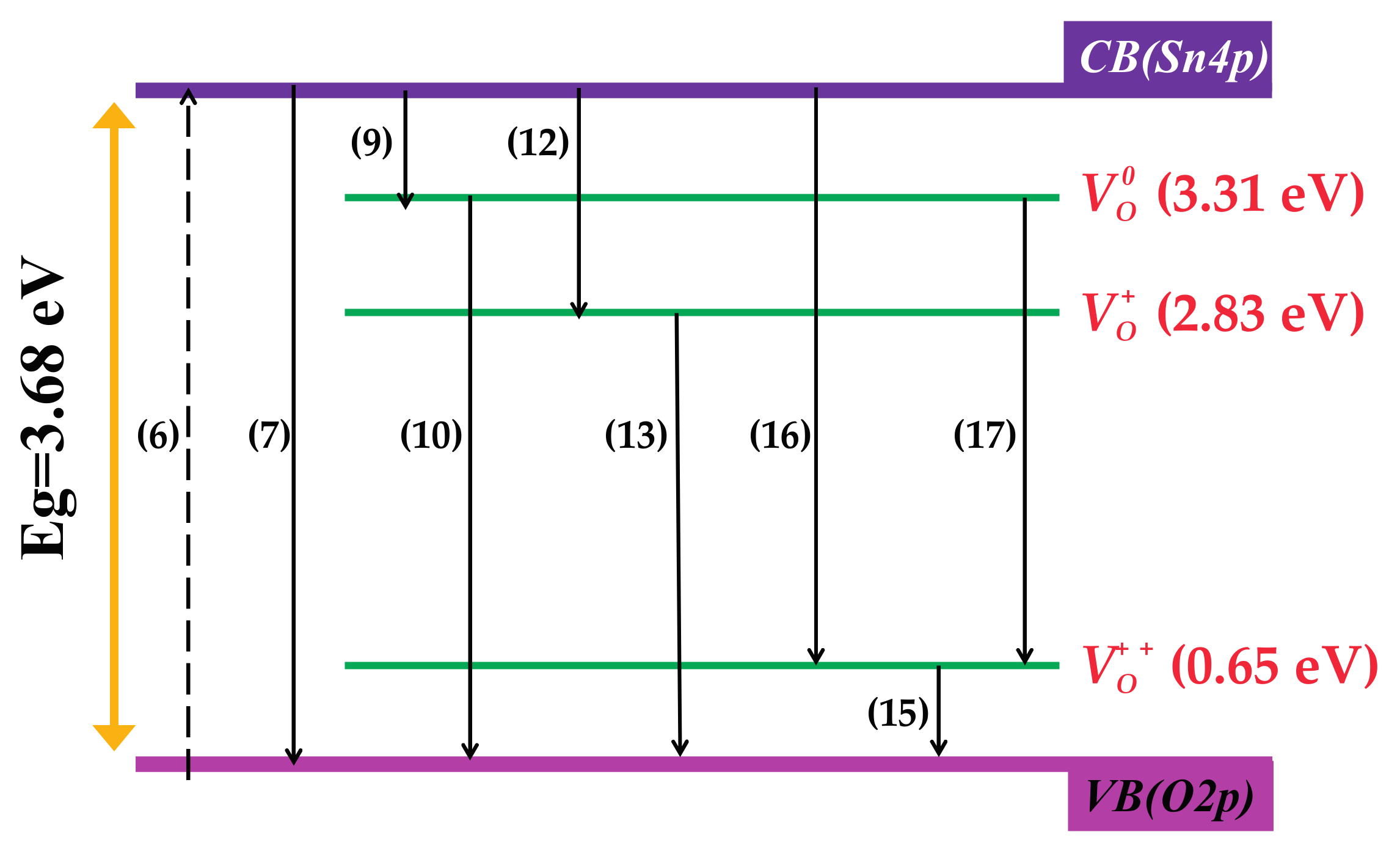
3.7. Investigation of Photoluminescence Mechanism
4. Conclusions
Acknowledgments
Author Contributions
Conflicts of interest
References
- Dymshits, A.; Iagher, L.; Etgar, L. Parameters influencing the growth of ZnO nanowires as efficient low temperature flexible perovskite-based solar cells. Materials 2016, 9, 60. [Google Scholar] [CrossRef] [PubMed]
- Maestre, D.; Cremades, A.; Piqueras, J. Cathodoluminescence of defects in sintered tin oxide. J. Appl. Phys. 2004, 95, 3027–3030. [Google Scholar] [CrossRef] [Green Version]
- García-Tecedor, M.; Maestre, D.; Cremades, A.; Piqueras, J. Influence of Cr doping on the morphology and luminescence of SnO2 nanostructures. J. Phys. Chem. C 2016, 120, 22028–22034. [Google Scholar] [CrossRef]
- Bouazizi, N.; Bargougui, R.; Boudharaa, T.; Khelil, M.; Benghnia, A.; Labiadh, L.; Benslama, R.; Chaouachi, B.; Ammar, S.; Azzouz, A. Synthesis and characterization of SnO2-HMD-Fe materials with improved electric properties and affinity towards hydrogen. Ceram. Int. 2016, 42, 9413–9418. [Google Scholar] [CrossRef]
- Hu, R.; Ouyang, Y.; Chen, D.; Wang, H.; Chen, Y.; Zhu, M.; Liu, M. Inhibiting Sn coarsening to enhance the reversibility of conversion reaction in lithiated SnO2 anodes by application of super-elastic niti films. Acta Mater. 2016, 109, 248–258. [Google Scholar] [CrossRef]
- Song, Y.L.; Jiang, W.F.; Ji, P.F.; Li, Y.; Zhou, F.Q.; Wen, N. A prototypical nanostructured ZnO/Si light-emitting diode based on the silicon nanoporous pillar array: Carriers transportation properties and white electroluminescence. J. Lumin. 2017, 192, 734–738. [Google Scholar] [CrossRef]
- Pal, S.; Sarkar, A.; Kumar, P.; Kanjilal, D.; Rakshit, T.; Ray, S.K.; Jana, D. Low temperature photoluminescence from disordered granular ZnO. J. Lumin. 2016, 169, 326–333. [Google Scholar] [CrossRef]
- Yang, Y.; Li, S.; Liu, F.; Zhang, N.; Liu, K.; Wang, S.; Fang, G. Bidirectional electroluminescence from p-SnO2/i-MgZnO/n-ZnO heterojunction light-emitting diodes. J. Lumin. 2017, 186, 223–228. [Google Scholar] [CrossRef]
- Shewale, P.S.; Ung Sim, K.; Kim, Y.-b.; Kim, J.H.; Moholkar, A.V.; Uplane, M.D. Structural and photoluminescence characterization of SnO2:F thin films deposited by advanced spray pyrolysis technique at low substrate temperature. J. Lumin. 2013, 139, 113–118. [Google Scholar] [CrossRef]
- Kaur, J.; Shah, J.; Kotnala, R.K.; Verma, K.C. Raman spectra, photoluminescence and ferromagnetism of pure, Co and Fe doped SnO2 nanoparticles. Ceram. Int. 2012, 38, 5563–5570. [Google Scholar] [CrossRef]
- Mrabet, C.; Boukhachem, A.; Amlouk, M.; Manoubi, T. Improvement of the optoelectronic properties of tin oxide transparent conductive thin films through lanthanum doping. J. Alloys Compd. 2016, 666, 392–405. [Google Scholar] [CrossRef]
- Zhou, G.X.; Xiong, S.J.; Wu, X.L.; Liu, L.Z.; Li, T.H.; Chu, P.K. N-doped SnO2 nanocrystals with green emission dependent upon mutual effects of nitrogen dopant and oxygen vacancy. Acta Mater. 2013, 61, 7342–7347. [Google Scholar] [CrossRef]
- Peche-Herrero, M.A.; Maestre, D.; Ramírez-Castellanos, J.; Cremades, A.; Piqueras, J.; González-Calbet, J.M. The controlled transition-metal doping of SnO2 nanoparticles with tunable luminescence. CrystEngComm 2014, 16, 2969–2976. [Google Scholar] [CrossRef]
- Ni, J.; Zhao, X.; Zheng, X.; Zhao, J.; Liu, B. Electrical, structural, photoluminescence and optical properties of p-type conducting, antimony-doped SnO2 thin films. Acta Mater. 2009, 57, 278–285. [Google Scholar] [CrossRef]
- Ahmed, A.S.; Shafeeq, M.M.; Singla, M.L.; Tabassum, S.; Naqvi, A.H.; Azam, A. Band gap narrowing and fluorescence properties of nickel doped SnO2 nanoparticles. J. Lumin. 2011, 131, 1–6. [Google Scholar] [CrossRef]
- Pei, X.; Ji, F.; Ma, J.; Ning, T.; Song, Z.; Tan, Y.; Luan, C. Structural and photoluminescence properties of SnO2:Ga films deposited on α-Al2O3 (0001) by MOCVD. J. Lumin. 2010, 130, 1189–1193. [Google Scholar] [CrossRef]
- Wang, Y.; Ma, J.; Ji, F.; Yu, X.; Ma, H. Structural and photoluminescence characters of SnO2:Sb films deposited by RF magnetron sputtering. J. Lumin. 2005, 114, 71–76. [Google Scholar] [CrossRef]
- Ameur, S.B.; Barhoumi, A.; Bel hadjltaief, H.; Mimouni, R.; Duponchel, B.; Leroy, G.; Amlouk, M.; Guermazi, H. Physical investigations on undoped and fluorine doped SnO2 nanofilms on flexible substrate along with wettability and photocatalytic activity tests. Mater. Sci. Semicond. Process. 2017, 61, 17–26. [Google Scholar] [CrossRef]
- Yang, J.K.; Zhao, H.L.; Li, J.; Zhao, L.P.; Chen, J.J.; Yu, B. Structural and optical properties and photoluminescence mechanism of fluorine-doped SnO2 films during the annealing process. Acta Mater. 2014, 62, 156–161. [Google Scholar] [CrossRef]
- Thirumoorthi, M.; Prakash, J.T.J. Effect of F doping on physical properties of (211) oriented SnO2 thin films prepared by jet nebulizer spray pyrolysis technique. Superlattices Microstruct. 2016, 89, 378–389. [Google Scholar] [CrossRef]
- Yang, J.K.; Liang, B.; Zhao, M.J.; Gao, Y.; Zhang, F.C.; Zhao, H.L. Reference of temperature and time during tempering process for non-stoichiometric FTO films. Sci. Rep. 2015, 5, 15001. [Google Scholar] [CrossRef] [PubMed]
- Zhu, B.L.; Yang, Y.T.; Hu, W.C.; Wu, J.; Gan, Z.H.; Liu, J.; Zeng, D.W.; Xie, C.S. Transparent conductive F-doped SnO2 films prepared by RF reactive magnetron sputtering at low substrate temperature. Appl. Phys. A 2017, 123, 217. [Google Scholar] [CrossRef]
- Li, T.; Zhang, X.; Ni, J.; Fang, J.; Zhang, D.; Sun, J.; Wei, C.; Xu, S.; Wang, G.; Zhao, Y. Modify the schottky contact between fluorine-doped tin oxide front electrode and p-α-SiC:H by carbon dioxide plasma treatment. Sol. Energy 2016, 134, 375–382. [Google Scholar] [CrossRef]
- Consonni, V.; Rey, G.; Roussel, H.; Doisneau, B.; Blanquet, E.; Bellet, D. Preferential orientation of fluorine-doped SnO2 thin films: The effects of growth temperature. Acta Mater. 2013, 61, 22–31. [Google Scholar] [CrossRef]
- Ajili, M.; Castagné, M.; Kamoun Turki, N. Spray solution flow rate effect on growth, optoelectronic characteristics and photoluminescence of SnO2:F thin films for photovoltaic application. Optik Int. J. Light Electron Opt. 2015, 126, 708–714. [Google Scholar] [CrossRef]
- Senna, M.; Turianicová, E.; Šepelák, V.; Bruns, M.; Scholz, G.; Lebedkin, S.; Kübel, C.; Wang, D.; Kaňuchová, M.; Kaus, M.; et al. Fluorine incorporation into SnO2 nanoparticles by Co-milling with polyvinylidene fluoride. Solid State Sci. 2014, 30, 36–43. [Google Scholar] [CrossRef]
- Yu, S.; Li, L.; Lyu, X.; Zhang, W. Preparation and investigation of nano-thick FTO/Ag/FTO multilayer transparent electrodes with high figure of merit. Sci. Rep. 2016, 6, 20399. [Google Scholar] [CrossRef] [PubMed]
- El Akkad, F.; Paulose, T.A.P. Optical transitions and point defects in F:SnO2 films: Effect of annealing. Appl. Surf. Sci. 2014, 295, 8–17. [Google Scholar] [CrossRef]
- Bhattacharjee, A.; Ahmaruzzaman, M.; Sil, A.K.; Sinha, T. Amino acid mediated synthesis of luminescent SnO2 nanoparticles. J. Ind. Eng. Chem. 2015, 22, 138–146. [Google Scholar] [CrossRef]
- Kumar, V.; Singh, K.; Kumar, A.; Kumar, M.; Singh, K.; Vij, A.; Thakur, A. Effect of solvent on crystallographic, morphological and optical properties of SnO2 nanoparticles. Mater. Res. Bull. 2017, 85, 202–208. [Google Scholar] [CrossRef]
- Gao, F.; Li, Y.; Zhao, Y.; Wan, W.; Du, G.; Ren, X.; Zhao, H. Facile synthesis of flower-like hierarchical architecture of SnO2 nanoarrays. J. Alloys Compd. 2017, 703, 354–360. [Google Scholar] [CrossRef]
- Liu, L.Z.; Wu, X.L.; Xu, J.Q.; Li, T.H.; Shen, J.C.; Chu, P.K. Oxygen-vacancy and depth-dependent violet double-peak photoluminescence from ultrathin cuboid SnO2 nanocrystals. Appl. Phys. Lett. 2012, 100, 121903. [Google Scholar] [CrossRef]
- Liu, L.Z.; Wu, X.L.; Gao, F.; Shen, J.C.; Li, T.H.; Chu, P.K. Determination of surface oxygen vacancy position in SnO2 nanocrystals by Raman spectroscopy. Solid State Commun. 2011, 151, 811–814. [Google Scholar] [CrossRef]
- Kar, A.; Kundu, S.; Patra, A. Surface defect-related luminescence properties of SnO2 nanorods and nanoparticles. J. Phys. Chem. C 2011, 115, 118–124. [Google Scholar] [CrossRef]
- Deepu, D.R.; Sudha Kartha, C.; Vijayakumar, K.P. How spray rate influences the formation and properties of transparent conducting SnO2 thin films. J. Anal. Appl. Pyrolysis 2016, 121, 24–28. [Google Scholar] [CrossRef]
- Baraneedharan, P.; Imran Hussain, S.; Dinesh, V.P.; Siva, C.; Biji, P.; Sivakumar, M. Lattice doped Zn–SnO2 nanospheres: A systematic exploration of dopant ion effects on structural, optical, and enhanced gas sensing properties. Appl. Surf. Sci. 2015, 357, 1511–1521. [Google Scholar] [CrossRef]
- Gu, F.; Wang, H.; Han, D.; Wang, Z. Enhancing the sensing performance of SnO2 inverse opal thin films by In and Au doping. Sens. Actuators B Chem. 2017, 245, 1023–1031. [Google Scholar] [CrossRef]
- Reddy, C.V.; Babu, B.; Vattikuti, S.V.P.; Ravikumar, R.V.S.S.N.; Shim, J. Structural and optical properties of vanadium doped SnO2 nanoparticles with high photocatalytic activities. J. Lumin. 2016, 179, 26–34. [Google Scholar] [CrossRef]
- Agrahari, V.; Mathpal, M.C.; Kumar, M.; Agarwal, A. Investigations of optoelectronic properties In DMS SnO2 nanoparticles. J. Alloys Compd. 2015, 622, 48–53. [Google Scholar] [CrossRef]
- Xu, M.; Ruan, X.; Yan, J.; Zhang, Z.; Yun, J.; Zhao, W.; Li, T.; Shi, Y. Synthesis, growth mechanism, and photoluminescence property of hierarchical SnO2 nanoflower-rod arrays: An experimental and first principles study. J. Mater. Sci. 2016, 51, 9613–9624. [Google Scholar] [CrossRef]
- Trani, F.; Causà, M.; Ninno, D.; Cantele, G.; Barone, V. Density functional study of oxygen vacancies at the SnO2 surface and subsurface sites. Phys. Rev. B 2008, 77, 245210. [Google Scholar] [CrossRef]


| Samples | D-Spacing | Lattice Parameters | Daver (nm) | ||||
|---|---|---|---|---|---|---|---|
| d110 (Å) | d101 (Å) | d211 (Å) | a (Å) | c (Å) | V (Å3) | ||
| PDF#71-0652 | 3.350 | 2.644 | 1.764 | 4.738 | 3.187 | 71.5 | — |
| Undoped | 3.351 | 2.647 | 1.763 | 4.730 | 3.194 | 71.44 | 20.18 |
| 10 at. % | 3.351 | 2.650 | 1.765 | 4.731 | 3.198 | 71.60 | 18.19 |
| 30 at. % | 3.356 | 2.653 | 1.763 | 4.718 | 3.208 | 71.41 | 17.08 |
| 50 at. % | 3.343 | 2.647 | 1.761 | 4.718 | 3.197 | 71.16 | 16.59 |
| Samples | Undoped | 10 at. % | 30 at. % | 50 at. % |
|---|---|---|---|---|
| Eg (eV) | 3.633 | 3.681 | 3.682 | 3.684 |
| Sample | O1s | Relative Content of Oα | |||
|---|---|---|---|---|---|
| Relative Content | Gaussian Peak | Peak Position (eV) | Area (%) | ||
| Undoped | 16.3 at. % | Oab | 530.9 | 14.85 | 4.04 at. % |
| Oα | 529.99 | 24.78 | |||
| Oβ | 529.01 | 60.37 | |||
| 10 at. % | 18.55 at. % | Oab | 531.3 | 12.2 | 5.5 at. % |
| Oα | 530.33 | 29.66 | |||
| Oβ | 529.32 | 58.13 | |||
| 30 at. % | 24.36 at. % | Oab | 532.02 | 15.46 | 6.12 at. % |
| Oα | 531.25 | 25.12 | |||
| Oβ | 530.37 | 59.42 | |||
| 50 at. % | 21.55 at. % | Oab | 531.46 | 13.64 | 4.45 at. % |
| Oα | 530.58 | 20.67 | |||
| Oβ | 529.71 | 65.69 | |||
© 2017 by the authors. Licensee MDPI, Basel, Switzerland. This article is an open access article distributed under the terms and conditions of the Creative Commons Attribution (CC BY) license (http://creativecommons.org/licenses/by/4.0/).
Share and Cite
Wang, X.; Wang, X.; Di, Q.; Zhao, H.; Liang, B.; Yang, J. Mutual Effects of Fluorine Dopant and Oxygen Vacancies on Structural and Luminescence Characteristics of F Doped SnO2 Nanoparticles. Materials 2017, 10, 1398. https://doi.org/10.3390/ma10121398
Wang X, Wang X, Di Q, Zhao H, Liang B, Yang J. Mutual Effects of Fluorine Dopant and Oxygen Vacancies on Structural and Luminescence Characteristics of F Doped SnO2 Nanoparticles. Materials. 2017; 10(12):1398. https://doi.org/10.3390/ma10121398
Chicago/Turabian StyleWang, Xiaolong, Xuan Wang, Qingyin Di, Hongli Zhao, Bo Liang, and Jingkai Yang. 2017. "Mutual Effects of Fluorine Dopant and Oxygen Vacancies on Structural and Luminescence Characteristics of F Doped SnO2 Nanoparticles" Materials 10, no. 12: 1398. https://doi.org/10.3390/ma10121398