Effects of UV-Ozone Treatment on Sensing Behaviours of EGFETs with Al2O3 Sensing Film

1
State Key Laboratory of ASIC and System, Fudan University, Shanghai 200433, China
2
School of Information Science and Technology, Fudan University, Shanghai 200433, China
*
Authors to whom correspondence should be addressed.
Materials 2017, 10(12), 1432; https://doi.org/10.3390/ma10121432
Submission received: 22 October 2017
/
Revised: 23 November 2017
/
Accepted: 13 December 2017
/
Published: 15 December 2017
Abstract
:The effects of UV-ozone (UVO) treatment on the sensing behaviours of extended-gate field-effect transistors (EGFETs) that use Al2O3 as the sensing film have been investigated. The Al2O3 sensing films are UVO-treated with various duration times and the corresponding EGFET sensing behaviours, such as sensitivity, hysteresis, and long-term stability, are electrically evaluated under various measurement conditions. Physical analysis is also performed to characterize the surface conditions of the UVO-treated sensing films using X-ray photoelectron spectroscopy and atomic force microscopy. It is found that UVO treatment effectively reduces the buried sites in the Al2O3 sensing film and subsequently results in reduced hysteresis and improved long-term stability of EGFET. Meanwhile, the observed slightly smoother Al2O3 film surface post UVO treatment corresponds to decreased surface sites and slightly reduced pH sensitivity of the Al2O3 film. The sensitivity degradation is found to be monotonically correlated with the UVO treatment time. A treatment time of 10 min is found to yield an excellent performance trade-off: clearly improved long-term stability and reduced hysteresis at the cost of negligible sensitivity reduction. These results suggest that UVO treatment is a simple and facile method to improve the overall sensing performance of the EGFETs with an Al2O3 sensing film.
1. Introduction
The ion-sensitive field-effect transistor (ISFET) was first developed by Bergveld in 1970, which were initially used for pH detection and ion concentration measurement [1,2]. ISFETs are potentiometric devices based on the structure of the metal-oxide-semiconductor field-effect transistor (MOSFET) by removing the metal gate of the MOSFET [1,2,3]. When an ISFET is used for pH sensing, the electric potential at the insulator/electrolyte interface will be controlled by the hydrogen ion concentration with the bare oxide contacting the chemical environment [3,4]. As a modified category of the ISFET, extended-gate field-effect transistor (EGFET) based on the same working principle of the ISFET is comprised of a sensing structure and a conventional MOSFET [5,6]. The sensing structure with a sensing film contacting the electrolyte directly is connected to the FET metal gate by a metal signal line. Without immersing the FET in the electrolyte and removing the metal gate, the EGFET presents better thermal stability and light stability compared to the ISFET [6,7,8,9]. The EGFET allows the reuse of the MOSFET and a flexible shape of the sensing structure. Over these years, materials used as EGFET sensing films have been investigated, such as tin dioxide (SnO2), tantalum pentoxide (Ta2O5), vanadium pentoxide (V2O5), and so on [7,9,10]. Among these materials, Al2O3 is considered as a suitable sensing material from the point of view of its inert characteristic, high sensitivity, good ion selectivity, and compatibility with the complementary metal oxide semiconductor (CMOS) process [11]. With the advantages of light insensitivity, easy fabrication, low cost, and disposable gate, EGFETs have drawn a great deal of attention and a wide range of applications based on EGFETs have been reported [5,6,7,8,9,12,13,14,15]. However, several instability phenomena related to the sensing film still exist which limits the measurement precision when an EGFET is used for pH sensing [16,17]. According to previous studies [17,18,19,20,21,22], the instability is mainly caused by defects in the sensing film, such as buried sites, charge traps, and slow-reacting surface sites. For example, hysteresis can be attributed to buried sites near the sensing film surface [22]. Hysteresis leads to a response deviation between identical pH measurement conditions, causing an unreliable measurement output [17,23]. Therefore, it is necessary to utilize a high-quality film with few defects as the sensing film [24]. It is generally accepted that the sensing mechanism can be explained with site dissociation model, meaning that the reaction between hydrogen in the electrolyte and amphoteric groups takes place at the surface of the sensing film [4,25,26]. The quality of the sensing film surface demonstrably plays a significant role in EGFET sensing behaviours and is sensitive to surface contamination, surface morphology, and defects. To improve the quality of sensing film, several surface modification methods have been attempted, including oxygen plasma, SF6 plasma, wet chemical treatment, and the texturization of the sensing film [24,27,28,29,30,31]. Among these surface treatment methods, UV-ozone (UVO) treatment is a typical method for surface cleaning or surface activation during sensor fabrication [32,33,34,35,36,37,38,39,40,41]. UVO treatment is reportedly capable of removing organic contaminants and has the advantages of being a dry cleaning agent, easy to use, harmless to the environment, and compatible with the CMOS process [42,43].
In order to investigate the comprehensive effects of UVO treatment in EGFET sensing behaviours, this study conducted a series of experiments with various UVO treatment times on Al2O3 sensing film. With the introduction of the UVO treatment, a large enhancement on sensing performance was observed, especially in the reduction of hysteresis. In order to clarify the mechanism of UVO treatment, X-ray photoelectron spectroscopy (XPS) and atomic force microscopy (AFM) were utilized to analyse surface composition and morphology. XPS and AFM results confirmed that a cleaner and smoother Al2O3 sensing film surface was obtained after UVO treatment. Moreover, the –OH groups involved in the Al2O3 deposition process had been removed. Resultantly, an optimal UVO treatment time was, therefore, obtained.
2. Materials and Methods
2.1. Fabrication Process
The following is the process by which EGFET fabrication based on Al2O3 sensing film was achieved. The EGFET is separated into two parts: one is a sensing structure with an extended gate and the other is a commercial MOSFET. The sensing structure has a glass substrate, and a metal electrode is deposited on the substrate, which is connected to the metal gate of the MOSFET. When the sensing film contacts with the electrolyte, electric potential at the sensing film surface will vary with the ion concentration. Therefore, the electric potential variation at electrolyte/insulator interface will be detected by the MOSFET. To fabricate the sensing structure, the glass substrate (CORNING EAGLE XG®, CORNING, New York, NY, USA) was cleaned with standard RCA cleaning process, and 50 nm titanium (Ti) and 500 nm aluminium (Al) were deposited on the substrate using electron beam evaporation as an electrode. Next, 50 nm Al2O3 films were deposited by atomic layer deposition (ALD) on the Ti/Al electrode under 300 °C. The thickness of Al2O3 film was analysed by an ellipsometer. The dimension of Al2O3 films was 2 cm in length and 1.2 cm in width. Then, the sensing structures were treated with a UVO cleaner (BZZ250G-T, HWOTECH, Shenzhen, China). The UV intensity was 25 mW/cm2 at 254 nm, and ozone was generated in air atmosphere by absorbing 185 nm UV radiation. After UVO treatment, the sensing structures were pasted on the copper line of a printed circuit board (PCB) with adhesive tape. After bonding with the metal pad of the PCB, an epoxy resin adhesive of 200 nm thickness was coated on the sensing film surface following an elliptical path using a dispensing robot (TH-2004D-K, Tianhao, Zhejiang, China), which served as a container for the flow of liquid, as well as for sealing. When the epoxy was dry, a poly(methyl methacrylate) (PMMA) board was placed on it and fixed with screws on the four corners of the PCB. Finally, as shown in Figure 1a, this PCB was connected to a commercial n-channel power MOSFET gate (MMFT960T1, ON Semiconductor Corporation, Phoenix, AZ, USA) on a test board using pins.
2.2. Electrical and Physical Measurements
The device diagram and electrical measurement setup are demonstrated in Figure 1b. A stable environment for pH measurement was maintained by controlling the flow channel microfluidically. The Ag/AgCl electrode was inserted in the pH buffer solution for use as a reference electrode. Next, standard pH buffer solutions (Reagecon, Shannon, Ireland) with pH values varying from 4 to 9 were used for pH measurement. The electrolyte/insulator interface that all the samples were immersed in was stabilized in the buffer solution (pH 7) for at least 24 h before pH measurement. The electrochemical characteristics of the ALD Al2O3 EGFETs were obtained using a Keithley 4200-SCS semiconductor parameter analyser (Keithley, Cleveland, OH, USA). In the steady-state measurement, a reference voltage (Vref) applied at the Ag/AgCl reference electrode was swept from −1 V to 5 V with a step size of 0.01 V and then backwards, while a constant source-drain voltage was kept at 0.1 V. In the real-time measurement condition, the device was operated in the linear region by setting the reference voltage Vref at 3.5 V. As the pH in the loop changed from pH 9 to pH 4 and back, the source-drain current (Ids) was measured. Each pH value was held constant for 60 s before being altered and this measurement was controlled by an electromagnetic valve. The sensing behaviours of the devices were monitored over a period of three weeks. Using this methodology, the sensing behaviours of sensitivity, hysteresis, and stability were obtained. To acquire comprehensive knowledge of the material surface condition, XPS analysis and AFM analyses were also performed. The surface content was analysed by a Kratos AXIS Ultra DLD XPS (Kratos, Kyoto, Japan) using an Al Kα X-ray source (1486.6 eV). The surface morphology was determined using a Bruker Dimension Icon AFM (Bruker, Karlsruhe, Germany) over a scan area of 5 × 5 μm2 in tapping mode under ambient conditions. The AFM images were taken in the centre of the sensing film for each sample.
3. Results and Discussion
3.1. EGFET Sensing Behaviours
Figure 2 illustrates the transfer and sensitivity characteristics of EGFETs over different UVO treatment times. As shown in the left diagram of Figure 2a–e, the transfer curves shifted positively as the pH increased, reflecting the surface potential of the sensing film increasing with hydrogen ion concentration. The threshold voltage Vth of the EGFETs was defined as Vref when the drain current reached 1 × 10⁻⁷ A, and sensitivity was obtained by linearly fitting Vth with different pH values.
According to past studies [44,45,46], the sensitivity can be expressed as:
where k is the Boltzmann’s constant, T is the absolute temperature, q is the elementary charge, βint is the intrinsic buffer capacity, and Cdi is the differential capacitance. The experiment was carried out at room temperature. Sensitivity is influenced by two key parameters: buffer capacity βint and differential capacitance Cdi [45]. βint characterizes the ability of the surface to buffer small pH changes at the sensing film surface, which depends solely on the intrinsic properties of the sensing material, i.e., the equilibrium constants of Ka and Kb and the surface site number Ns [25,45]. βint can be expressed as:
As for Al2O3, the related parameters were set as Ka = 10−10 and Kb = 10−6 [46]. Cdif is defined as:
where c is the electrolyte concentration (c = 0.1 mol−1) and εw is the dielectric electrolyte constant (εw = 78.5).
Therefore, Cdi can be set to the constant value Cdi = 16 μF/cm2 as discussed in [25,44,45]. When surface amphoteric groups react with hydrogen ions, the surface sites exist in three forms: Al-O−, Al-OH2+ and Al-OH [44,46]. Therefore, surface site number Ns is the sum of these three sites [44,46]. Based on Equations (1)–(3), Ns can be calculated from the measured sensitivity in our experiment. Figure 2f shows that a reduced Ns caused by UVO treatment results in a decreased sensitivity. The Ns of 30-min UVO-treated Al2O3 film is 6.06 × 1013 cm−2, which is 8% smaller than that of the as-fabricated one. And the 30-min UVO-treated sample has the smallest sensitivity of 50 mV/pH, which is decreased by 17% compared with the untreated one. Therefore, Ns as well as sensitivity, shows an obvious degradation with long time exposure to UVO. With short time exposure to UVO, the reduction of Ns is smaller than 3% and sensitivity presents a small degradation. It can be seen in Figure 2f that Ns shows a monotonic decay with increased treatment time, and sensitivity is strongly correlated with Ns.
To acquire further knowledge of EGFET sensing behaviours, a real-time measurement was performed using a stepwise pH progression from pH 9 to pH 4, and back, while keeping Vref constant. It is shown in Figure 3a that all the pH loops in the real-time curve for each device are reproducible. The shift of threshold voltage ΔVth was calculated using the transconductance gm, . As demonstrated in Figure 3b, ΔVth does not coincided with the same pH in the sensing loop, leading to a so-called hysteresis phenomenon. Here, the hysteresis width is defined as the deviation between ΔVth from the neighbouring pH 7.
Table 1 shows the hysteresis width varying with UVO treatment time. All devices with the UVO treatment can be seen to have a smaller hysteresis as compared to the as-fabricated one. The smallest hysteresis was obtained in the 10-min UVO-treated device, which reached 10 mV, about 66% smaller than that of the untreated one. When the treatment time lasts for over 10 min, the hysteresis increases again and approaches the value of the untreated device. UVO treatment can, therefore, be used to effectively decrease EGFET hysteresis with an optimal time of 10 min. In generally, the EGFET response to pH variation happens in milliseconds, which is characterized by fast response [19,22,47]. However, there is an extra time needed for a saturated response, where slow response or hysteresis takes place and causes a response delay in the order of minutes to hours after pH variation [22]. It is commonly accepted that a fast response is dominated by the surface effect, where surface amphoteric groups react with hydrogen ions in the electrolyte. As for hysteresis, it is attributed to defects in the sensing film, which have a slow response to pH variation. These defects can be explained in terms of the interior OH sites in the sensing film, which are created during the fabrication process or exposure to the electrolyte [22]. Since those sites are located beneath the sensing film surface, it takes a longer time for the bulk response between buried sites and hydration ions [22,48]. With regard to the Al2O3 sensing film deposited by ALD, it is well known that Al-OH bonds are formed during reaction between trimethylaluminum (TMA) and H2O [49,50,51]. It is reasonable to ascribe the presence of interior OH sites to Al-OH caused by deposition. These buried OH sites near the sensing film surface can also respond to pH variation, which incurs hysteresis. It can be inferred that the O-H bond will be broken under the radiation of UV light, which results in Al-OH reduction [50,52,53,54].
To investigate the long-term stability of UVO-treated devices, sensing behaviours were evaluated continuously over three weeks. The comparisons of sensitivity and hysteresis characteristics during three weeks’ time are shown in Figure 4. The performance of untreated devices degraded with time and their sensitivity was reduced to 56 mV/pH. The sensing performance of 10-min UVO-treated devices was consistent over three weeks’ time, showing no remarkable degradation in sensitivity and hysteresis. By contrast, 5-min, 15-min, and 30-min UVO-treated devices were not equipped with good long-term stability and their sensitivity decreased or hysteresis increased within the three week period. As a result, the device with UVO treatment for 10 min provides a stable overall sensing performance over a long period of time. With extended exposure to UVO, the sensing film may be covered by a corrosive mist in the presence of water vapour or nitrogen and sulphur oxides in the air [52,53,54]. Therefore, the device shows a certain degree of degeneration when treatment time exceeds 10 min.
3.2. Sensing Film Surface Analysis
To clarify the mechanism underlying the UVO treatment, surface analysis was conducted using XPS and AFM. XPS was used to investigate the chemical composition of Al2O3 films with different treatment times. The O 1s core level spectra are shown in Figure 5a–e. According to the Gaussian fitting, the O 1s peak is de-convoluted into two components: one at 531.9 ± 0.1 eV, corresponding to Al-OH bonds, and the other at 531.0 eV, corresponding to Al-O-Al bonds. Table 2 provides detailed composition information for the Al2O3 films. The area ratio of Al-O-Al to Al-OH became higher and the surface carbon element became lower as UVO treatment time increased. As mentioned above, the Al-OH bonds were introduced into the Al2O3 films when TMA reacted with H2O during the ALD process [50,51]. The –OH groups near the surface acted as buried sites resulting in hysteresis, so hysteresis was reduced with –OH groups decreasing after the UVO treatment [22,50]. However, hysteresis showed an increased tendency when treatment time exceeded 10 min. The non-monotonic behaviour of hysteresis can be explained in terms of nitride formation with prolonged treatment time, as shown in Figure 5f. The increase of nitride species resulted in hysteresis increasing [52,53,54]. The control of treatment time can help minimize the influence of nitride species and benefit from reduced Al-OH content. Therefore, an optimal treatment time of 10 min yielded the smallest hysteresis. Moreover, a cleaner surface was obtained when the surface carbon-related contaminates were removed by UVO. According to the XPS results, UVO treatment for an appropriate time can improve Al2O3 film quality as well as EGFET sensing performance by reducing –OH group content and surface contaminates.
To obtain full knowledge of UVO effects on sensitivity, AFM analysis is conducted. The sensing film surface morphology is shown in Figure 6a–e and surface roughness is characterized by Rq (root mean square) is considered as a function of UVO treatment time in Figure 6f. The change in Ns can be characterized by Rq from AFM image [28,55]. It is shown in Figure 6 that surface roughness gets smaller and the surface gets smoother with UVO treatment. The smallest Rq is observed in the 30-min UVO-treated samples, which was decreased by 16% compared with 2.22 nm of the untreated samples. Surface roughness of the Al2O3 samples decreased as a function of UVO treatment time, reflecting that Ns was reduced with UVO treatment, which caused the sensitivity degradation as discussed above. AFM results indicate that Ns is decreased with increased treatment time, which is consistent with Figure 2f.
4. Conclusions
The effects of UVO treatment on the sensing behaviours of EGFETs based on Al2O3 sensing film have been studied. With the introduction of UVO treatment, EGFETs exhibit excellent pH sensing characteristics, such as decreased hysteresis, good long-term stability, and high sensitivity. Though the sensitivity decreases with increasing treatment time, the lowest sensitivity is still 50 mV/pH under UVO treatment for 30 min. The AFM and XPS results reveal that smoother sensing film surface, as well as reduced carbon-related contaminations and a decreased number of buried sites in the sensing film are achieved after UVO treatment. As a result, UVO treatment is effective to provide a higher-quality sensing film with a cleaner and smooth surface, as well as fewer buried sites. Furthermore, the 10-min UVO-treated device exhibits smallest hysteresis, best long-term stability, and yet still high enough sensitivity. Hence, UVO treatment is a very promising technique to improve the quality of the sensing films, as well as overall sensing performance of the corresponding EGFETs.
Acknowledgments
This work was supported by the National Natural Science Foundation of China (Nos. 61474028, 61774042), Shanghai Municipal Natural Science Foundation (No. 17ZR1446500), National S and T Project 02 (No. 2013ZX02303-004), and the “First-Class Construction” project of Fudan University.
Author Contributions
Ruixue Zeng and Junkai Zhang designed and maintained the overall measurement system; Cuiling Sun performed the experiment, analysed the data, and wrote the paper; and Dongping Wu and Zhi-Jun Qiu revised the manuscript.
Conflicts of Interest
The authors declare no conflict of interest.
References
- Bergveld, P. Thirty years of ISFETOLOGY: What happened in the past 30 years and what may happen in the next 30 years. Sens. Actuators B Chem. 2003, 88, 1–20. [Google Scholar] [CrossRef]
- Bergveld, P. Development, operation, and application of the ion-sensitive field-effect transistor as a tool for electrophysiology. IEEE Trans. Biomed. Eng. 1972, 19, 342–351. [Google Scholar] [CrossRef] [PubMed]
- Chang-Soo Lee, S.K.K. Ion-Sensitive Field-Effect Transistor for Biological Sensing. Sensors 2009, 9, 7111–7131. [Google Scholar]
- Shinwari, M.W.; Deen, M.J.; Landheer, D. Study of the electrolyte-insulator-semiconductor field-effect transistor (EISFET) with applications in biosensor design. Microelectron. Reliab. 2007, 47, 2025–2057. [Google Scholar] [CrossRef]
- Spiegel, J.V.D.; Lauks, I.; Chan, P.; Babic, D. The extended gate chemically sensitive field effect transistor as multi-species microprobe. Sens. Actuators 1983, 4, 291–298. [Google Scholar] [CrossRef]
- Yang, C.M.; Wang, J.C.; Chiang, T.W.; Lin, Y.T.; Juan, T.W.; Chen, T.G.; Shih, M.Y.; Lue, C.E.; Lai, C.S. Hydrogen ion sensing characteristics of IGZO/Si electrode in EGFET. Int. J. Nanotechnol. 2013, 11, 15. [Google Scholar] [CrossRef]
- Chi, L.L.; Chou, J.C.; Chung, W.Y.; Sun, T.P.; Hsiung, S.K. Study on extended gate field effect transistor with tin oxide sensing membrane. Mater. Chem. Phys. 2000, 63, 19–23. [Google Scholar] [CrossRef]
- Yin, L.T.; Chou, J.C.; Chung, W.Y.; Sun, T.P.; Hsiung, S.K. Separate structure extended gate H+-ion sensitive field effect transistor on a glass substrate. Sens. Actuators B Chem. 2000, 71, 106–111. [Google Scholar] [CrossRef]
- Guerra, E.M.; Silva, G.R.; Mulato, M. Extended gate field effect transistor using V2O5 xerogel sensing membrane by sol–gel method. Solid State Sci. 2009, 11, 456–460. [Google Scholar] [CrossRef]
- Pinto, J.V.; Branquinho, R.; Barquinha, P.; Alves, E.; Martins, R.; Fortunato, E. Extended-Gate ISFETs Based on Sputtered Amorphous Oxides. J. Disp. Technol. 2013, 9, 729–734. [Google Scholar] [CrossRef]
- Abe, H.; Esashi, M.; Matsuo, T. ISFET’s using inorganic gate thin films. IEEE Trans. Electron Devices 1979, 26, 1939–1944. [Google Scholar] [CrossRef]
- Batista, P.D. An embedded measurement system for electrical characterization of EGFET as pH sensor. Meas. Sci. Technol. 2013, 25, 1233–1243. [Google Scholar] [CrossRef]
- Ahn, C.G.; Kim, A.; Chan, W.P.; Ah, C.S.; Yang, J.H.; Kim, T.Y.; Jang, M.; Sung, G.Y. Modified ion sensitive field effect transistor sensors having an extended gate on a thick dielectric. Appl. Phys. Lett. 2010, 96, 1294. [Google Scholar] [CrossRef]
- Huang, I. High-performance extended gate field-effect-transistor-based dissolved carbon dioxide sensing system with a packaged microreference electrode. J. Micro Nanolithogr. MEMS MOEMS 2014, 13, 4005–4014. [Google Scholar]
- Lin, Y.H.; Chu, C.P.; Lin, C.F.; Liao, H.H.; Tsai, H.H.; Juang, Y.Z. Extended-gate field-effect transistor packed in micro channel for glucose, urea and protein biomarker detection. Biomed. Microdevices 2015, 17, 1–9. [Google Scholar] [CrossRef] [PubMed]
- Khanna, V.K. Remedial and adaptive solutions of ISFET non-ideal behaviour. Sens. Rev. 2013, 33, 228–237. [Google Scholar] [CrossRef]
- Sasaki, Y.; Kawarada, H. Low drift and small hysteresis characteristics of diamond electrolyte-solution-gate FET. J. Phys. Appl. Phys. 2010, 43, 374020. [Google Scholar] [CrossRef]
- Woias, P.; Meixner, L.; Fröstl, P. Slow pH response effects of silicon nitride ISFET sensors. Sens. Actuators B Chem. 1998, 48, 501–504. [Google Scholar] [CrossRef]
- Tsai, C.-N.; Chou, J.-C.; Sun, T.-P.; Hsiung, S.-K. Study on the time-dependent slow response of the tin oxide pH electrode. IEEE Sens. J. 2006, 6, 1243–1249. [Google Scholar] [CrossRef]
- Lee, S.H.; Rasaiah, J.C. Proton transfer and the mobilities of the H+ and OH− ions from studies of a dissociating model for water. J. Chem. Phys. 2011, 135, 124505. [Google Scholar] [CrossRef] [PubMed]
- Grattarola, M.; Massobrio, G.; Martinoia, S. Modeling H+ -sensitive FETs with SPICE. IEEE Trans. Electron Devices 1992, 39, 813–819. [Google Scholar] [CrossRef]
- Bousse, L.; Bergveld, P. The role of buried OH sites in the response mechanism of inorganic-gate pH-sensitive ISFETs. Sens. Actuators 1984, 6, 65–78. [Google Scholar] [CrossRef]
- Chou, J.C.; Weng, C.Y. Sensitivity and hysteresis effect in Al2O3 gate pH-ISFET. Mater. Chem. Phys. 2001, 71, 120–124. [Google Scholar] [CrossRef]
- Berg, A.V.D.; Bergveld, P.; Reinhoudt, D.N.; Sudhölter, E.J. Sensitivity control of ISFETs by chemical surface modification. Sens. Actuators 1985, 8, 129–148. [Google Scholar] [CrossRef]
- Tarasov, A.; Wipf, M.; Stoop, R.L.; Bedner, K.; Fu, W.; Guzenko, V.A.; Knopfmacher, O.; Calame, M.; Schönenberger, C. Understanding the electrolyte background for biochemical sensing with ion-sensitive field-effect transistors. ACS Nano 2012, 6, 9291–9298. [Google Scholar] [CrossRef] [PubMed]
- Wang, L.; Bu, Y.; Ao, J.-P. Effect of oxygen plasma treatment on the performance of AlGaN/GaN ion-sensitive field-effect transistors. Diam. Relat. Mater. 2017, 73, 1–6. [Google Scholar] [CrossRef]
- Yin, L.-T.; Chou, J.-C.; Chung, W.-Y.; Sun, T.-P.; Hsiung, S.-K. Characteristics of silicon nitride after O/sub 2/plasma surface treatment for pH-ISFET applications. IEEE Trans. Biomed. Eng. 2001, 48, 340–344. [Google Scholar] [PubMed]
- Lu, T.F.; Wang, J.C.; Yang, C.M.; Chang, C.P.; Ho, K.I.; Ai, C.F.; Lai, C.S. Non-ideal effects improvement of SF 6 plasma treated hafnium oxide film based on electrolyte & ndash;insulator– semiconductor structure for pH-sensor application. Microelectron. Reliab. 2010, 50, 742–746. [Google Scholar]
- Dipalo, M.; Pietzka, C.; Denisenko, A.; El-Hajj, H.; Kohn, E. O-terminated nano-diamond ISFET for applications in harsh environment. Diam. Relat. Mater. 2008, 17, 1241–1247. [Google Scholar] [CrossRef]
- Dastidar, S.; Agarwal, A.; Kumar, N.; Bal, V. Sensitivity Enhancement of Electrolyte–Insulator–Semiconductor Sensors Using Mesotextured and Nanotextured Dielectric Surfaces. IEEE Sens. J. 2015, 15, 2039–2045. [Google Scholar] [CrossRef]
- Saengdee, P.; Chaisriratanakul, W.; Bunjongpru, W.; Sripumkhai, W.; Srisuwan, A.; Jeamsaksiri, W.; Hruanun, C.; Poyai, A.; Promptmas, C. Surface modification of silicon dioxide, silicon nitride and titanium oxynitride for lactate dehydrogenase immobilization. Biosens. Bioelectron. 2015, 67, 134–138. [Google Scholar] [CrossRef] [PubMed]
- Chen, S.; Bomer, J.G.; Carlen, E.T.; Berg, A.V.D. Al2O3/Silicon Nano ISFET with Near Ideal Nernstian Response. Nano Lett. 2011, 11, 2334–2341. [Google Scholar] [CrossRef] [PubMed]
- Spanu, A.; Lai, S.; Cosseddu, P.; Tedesco, M.; Martinoia, S.; Bonfiglio, A. An organic transistor-based system for reference-less electrophysiological monitoring of excitable cells. Sci. Rep. 2015, 5. [Google Scholar] [CrossRef] [PubMed] [Green Version]
- Lee, M.; Zine, N.; Baraket, A.; Zabala, M.; Campabadal, F.; Caruso, R.; Trivella, M.G.; Jaffrezic-Renault, N.; Errachid, A. A novel biosensor based on hafnium oxide: Application for early stage detection of human interleukin-10. Sens. Actuators B Chem. 2012, 175, 201–207. [Google Scholar] [CrossRef]
- Li, D.-C.; Yang, P.-H.; Lu, M.S.-C. CMOS open-gate ion-sensitive field-effect transistors for ultrasensitive dopamine detection. IEEE Trans. Electron Devices 2010, 57, 2761–2767. [Google Scholar] [CrossRef]
- Braik, M.; Dridi, C.; Ali, M.B.; Ali, M.; Abbas, M.; Zabala, M.; Bausells, J.; Zine, N.; Jaffrezic-Renault, N.; Errachid, A. Development of a capacitive chemical sensor based on Co (II)-phthalocyanine acrylate-polymer/HfO2/SiO2/Si for detection of perchlorate. J. Sens. Sens. Syst. 2015, 4, 17. [Google Scholar] [CrossRef]
- Braeken, D.; Rand, D.R.; Andrei, A.; Huys, R.; Spira, M.E.; Yitzchaik, S.; Shappir, J.; Borghs, G.; Callewaert, G.; Bartic, C. Glutamate sensing with enzyme-modified floating-gate field effect transistors. Biosens. Bioelectron. 2009, 24, 2384–2389. [Google Scholar] [CrossRef] [PubMed]
- Stoop, R.L.; Wipf, M.; Müller, S.; Bedner, K.; Wright, I.A.; Martin, C.J.; Constable, E.C.; Fanget, A.; Schönenberger, C.; Calame, M. Implementing Silicon Nanoribbon Field-Effect Transistors as Arrays for Multiple Ion Detection. Biosensors 2016, 6, 21. [Google Scholar] [CrossRef] [PubMed]
- Bhattacharyya, A.; Klapperich, C.M. Mechanical and chemical analysis of plasma and ultraviolet–ozone surface treatments for thermal bonding of polymeric microfluidic devices. Lab Chip 2007, 7, 876–882. [Google Scholar] [CrossRef] [PubMed]
- Kang, B.S.; Wang, H.T.; Ren, F.; Hlad, M.; Gila, B.P.; Abernathy, C.R.; Pearton, S.J.; Li, C.; Low, Z.N.; Lin, J. Role of gate oxide in AlGaN/GaN high-electron-mobility transistor pH sensors. J. Electron. Mater. 2008, 37, 550–553. [Google Scholar] [CrossRef]
- Yusilawati, A.N.; Maizirwan, M.; Hamzah, M.S.; Ng, K.H.; Wong, C.S. Surface modification of polystyrene beads by ultraviolet/ozone treatment and its effect on gelatin coating. Am. J. Appl. Sci. 2010, 7, 724–731. [Google Scholar] [CrossRef]
- Milgrew, M.J.; Cumming, D.R. Matching the transconductance characteristics of CMOS ISFET arrays by removing trapped charge. IEEE Trans. Electron Devices 2008, 55, 1074–1079. [Google Scholar] [CrossRef]
- Georgiou, P.; Toumazou, C. ISFET characteristics in CMOS and their application to weak inversion operation. Sens. Actuators B Chem. 2009, 143, 211–217. [Google Scholar] [CrossRef]
- Bousse, L.; De Rooij, N.F.; Bergveld, P. Operation of chemically sensitive field-effect sensors as a function of the insulator-electrolyte interface. IEEE Trans. Electron Devices 1983, 30, 1263–1270. [Google Scholar] [CrossRef]
- Van Hal, R.E.G.; Eijkel, J.C.T.; Bergveld, P. A novel description of ISFET sensitivity with the buffer capacity and double-layer capacitance as key parameters. Sens. Actuators B Chem. 1995, 24, 201–205. [Google Scholar] [CrossRef]
- Fung, C.D.; Cheung, P.W.; Ko, W.H. A generalized theory of an electrolyte-insulator-semiconductor field-effect transistor. IEEE Trans. Electron Devices 1986, 33, 8–18. [Google Scholar] [CrossRef]
- Woias, P.; Meixner, L.; Amandi, D.; Schönberger, M. Modelling the short-time response of ISFET sensors. Sens. Actuators B Chem. 1995, 24, 211–217. [Google Scholar] [CrossRef]
- Kim, Y.-J.; Lee, S.-G.; Yeo, J.-H.; Jo, Y.-W. Structural and Electrical Properties of an Electrolyte-insulator-metal Device with Variations in the Surface Area of the Anodic Aluminum Oxide Template for pH Sensors. J. Electr. Eng. Technol. 2015, 10, 2364–2367. [Google Scholar] [CrossRef]
- Ghiraldelli, E.; Pelosi, C.; Gombia, E.; Chiavarotti, G.; Vanzetti, L. ALD growth, thermal treatments and characterisation of Al2O3 layers. Thin Solid Films 2008, 517, 434–436. [Google Scholar] [CrossRef]
- Zhu, L.Q.; Liu, Y.H.; Zhang, H.L.; Xiao, H.; Guo, L.Q. Atomic layer deposited Al2O3 films for anti-reflectance and surface passivation applications. Appl. Surf. Sci. 2014, 288, 430–434. [Google Scholar] [CrossRef]
- Iatsunskyi, I.; Kempiński, M.; Jancelewicz, M.; Załęski, K.; Jurga, S.; Smyntyna, V. Structural and XPS characterization of ALD Al2O3 coated porous silicon. Vacuum 2015, 113, 52–58. [Google Scholar] [CrossRef]
- Kern, W. Science, Technology, and Applications. In Handbook of Semiconductor Wafer Cleaning Technology; Elsevier: Amsterdam, The Netherlands, 1993. [Google Scholar]
- Vig, J.R. UV/ozone cleaning of surfaces. J. Vac. Sci. Technol. 1985, 3, 1027–1034. [Google Scholar] [CrossRef]
- Moldovan, A.; Feldmann, F.; Krugel, G.; Zimmer, M.; Rentsch, J.; Hermle, M.; Roth-Fölsch, A.; Kai, K.; Hagendorf, C. Simple Cleaning and Conditioning of Silicon Surfaces with UV/Ozone Sources. Energy Procedia 2014, 55, 834–844. [Google Scholar] [CrossRef]
- Lu, T.F.; Chuang, H.C.; Wang, J.C.; Yang, C.M.; Kuo, P.C.; Lai, C.S. Effects of Thickness Effect and Rapid Thermal Annealing on pH Sensing Characteristics of Thin HfO2 Films Formed by Atomic Layer Deposition. Jpn. J. Appl. Phys. 2011, 50, 242–247. [Google Scholar] [CrossRef]
Figure 1.
(a) Image of sensing structure connected to a commercial MOSFET on a test board; and (b) a schematic diagram and the measurement setup of EGFETs.
Figure 1.
(a) Image of sensing structure connected to a commercial MOSFET on a test board; and (b) a schematic diagram and the measurement setup of EGFETs.
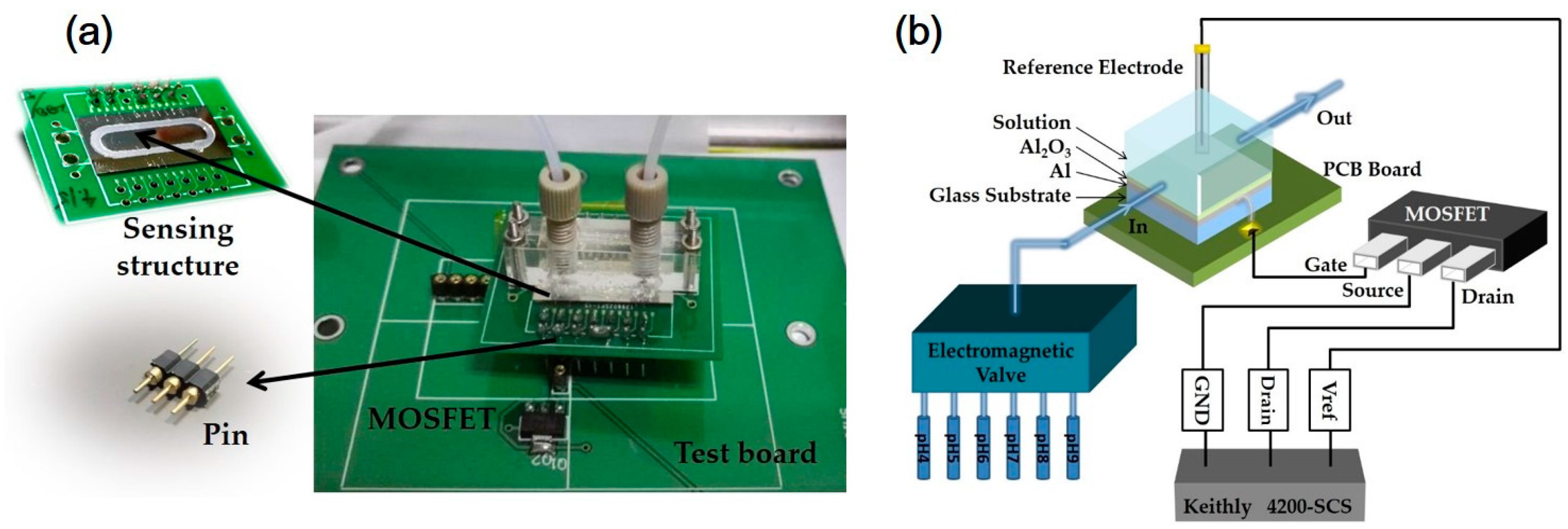
Figure 2.
Transfer characteristics, sensitivity and linearity of EGFETs using 50 nm-Al2O3: (a) without UVO treatment; and with UVO treatment for (b) 5; (c) 10; (d) 15; and (e) 30 min; and (f) a comparison of average sensitivity and Ns of three EGFETs (N = 3) without UVO treatment and with UVO treatment for 5, 10, 15, and 30 min.
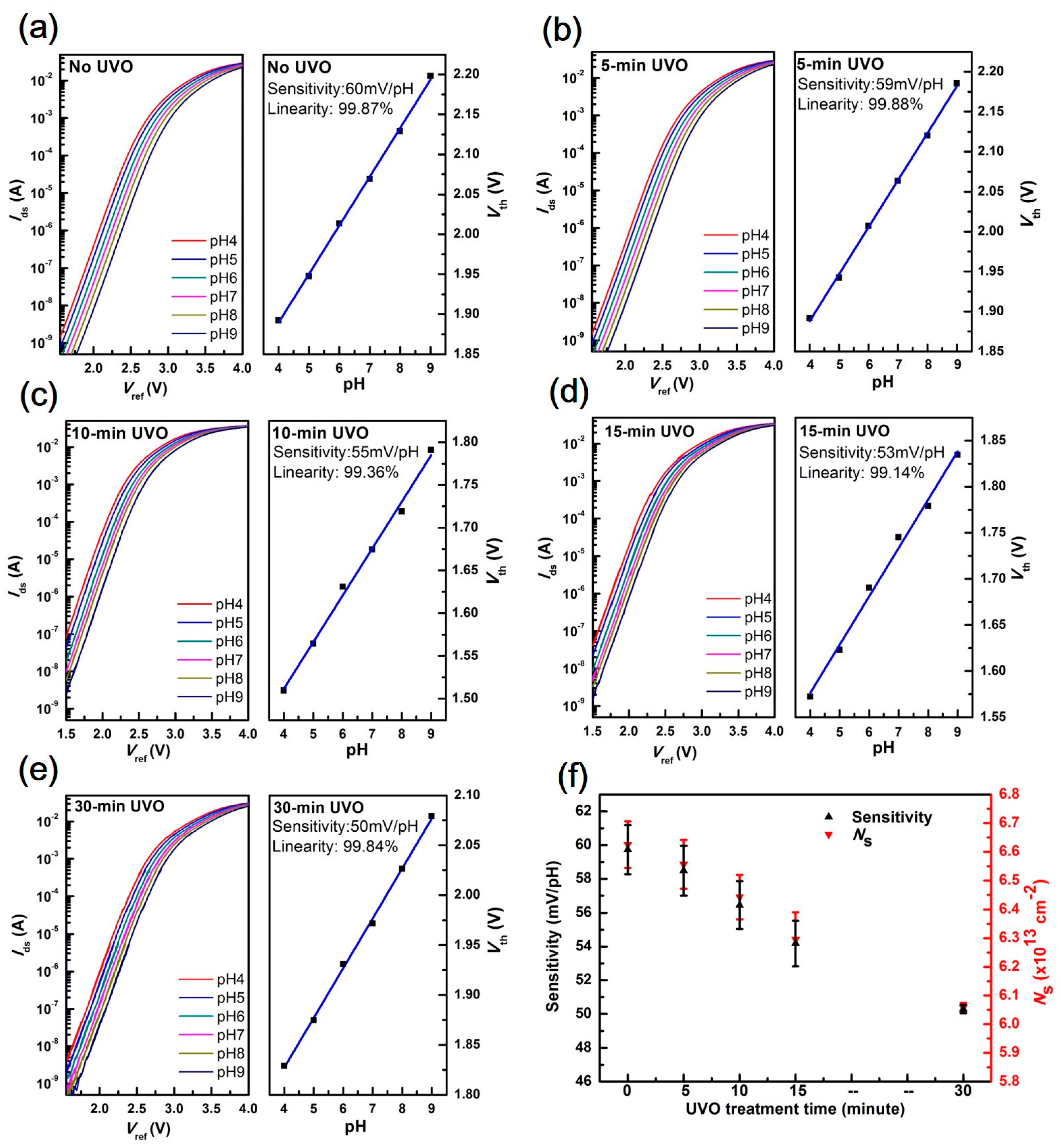
Figure 3.
(a) Real-time measurement results for EGFETs with different UVO treatments; and (b) real-time curve to evaluate hysteresis width at pH 7 over pH loops in the sequence pH 9–4 and pH 4–9.
Figure 3.
(a) Real-time measurement results for EGFETs with different UVO treatments; and (b) real-time curve to evaluate hysteresis width at pH 7 over pH loops in the sequence pH 9–4 and pH 4–9.
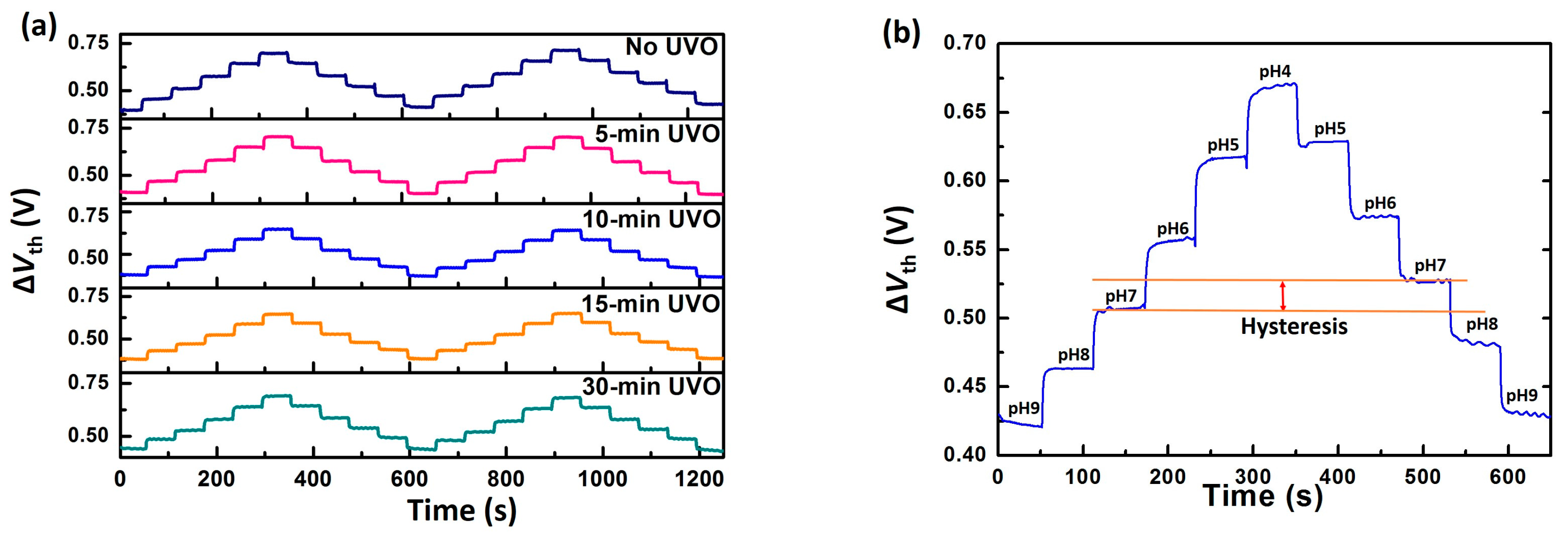
Figure 4.
(a) Hysteresis characteristics and (b) sensitivity characteristics of EGFETs using 50 nm-Al2O3 without and with UVO treatment over three weeks. The lines in (a) are guides to the eye.
Figure 4.
(a) Hysteresis characteristics and (b) sensitivity characteristics of EGFETs using 50 nm-Al2O3 without and with UVO treatment over three weeks. The lines in (a) are guides to the eye.
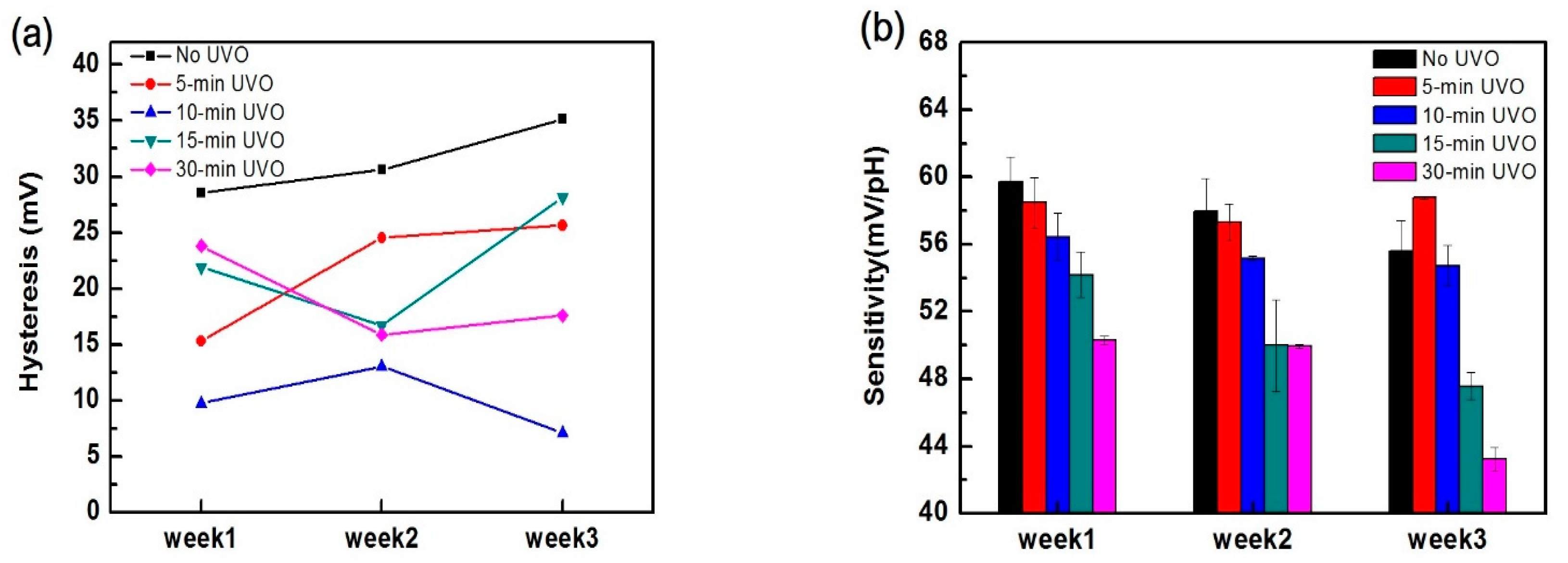
Figure 5.
XPS O 1s core level spectra of Al2O3: (a) without UVO treatment; and with UVO treatment for (b) 5; (c) 10; (d) 15; and (e) 30 min; and (f) XPS N 1s core level spectra of Al2O3 with different UVO treatment.
Figure 5.
XPS O 1s core level spectra of Al2O3: (a) without UVO treatment; and with UVO treatment for (b) 5; (c) 10; (d) 15; and (e) 30 min; and (f) XPS N 1s core level spectra of Al2O3 with different UVO treatment.
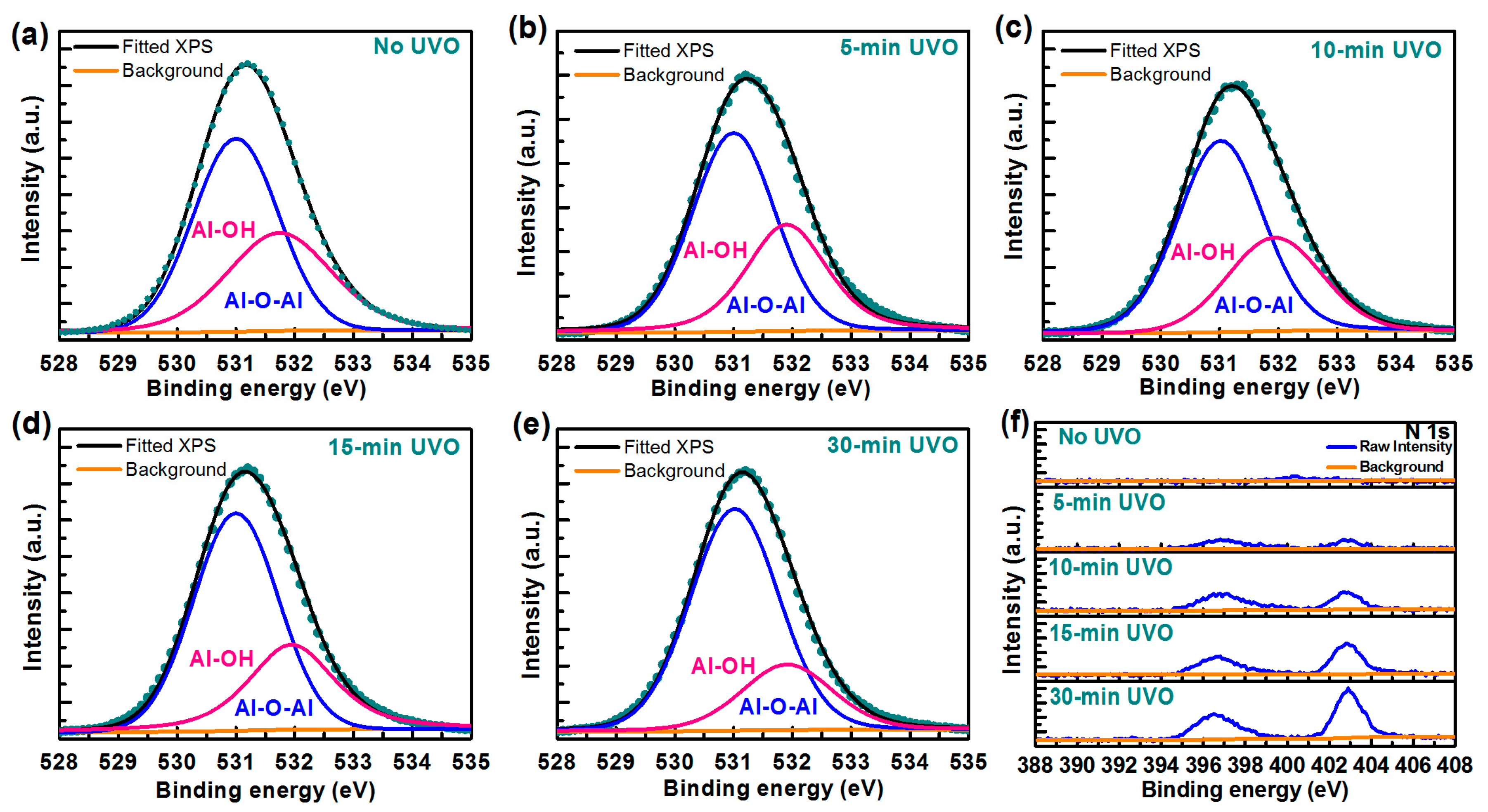
Figure 6.
AFM images of Al2O3 (a) without UVO treatment and with UVO treatment for (b) 5; (c) 10; (d) 15; and (e) 30 min; and (f) Rq as a function of UVO treatment.
Figure 6.
AFM images of Al2O3 (a) without UVO treatment and with UVO treatment for (b) 5; (c) 10; (d) 15; and (e) 30 min; and (f) Rq as a function of UVO treatment.


Table 1.
Hysteresis characteristics of EGFETs using 50 nm-Al2O3 without UVO treatment and with UVO treatment for 5, 10, 15, and 30 min.
Table 1.
Hysteresis characteristics of EGFETs using 50 nm-Al2O3 without UVO treatment and with UVO treatment for 5, 10, 15, and 30 min.
| Treatment | No UVO | 5-min UVO | 10-min UVO | 15-min UVO | 30-min UVO |
|---|---|---|---|---|---|
| Hysteresis (mV) | 28 | 15 | 10 | 22 | 24 |
Table 2.
Elemental composition in the surface and bulk based on XPS measurement. Values are given in at %.
Table 2.
Elemental composition in the surface and bulk based on XPS measurement. Values are given in at %.
| Treatment | Surface | Bulk | ||
|---|---|---|---|---|
| C (Atom %) | Al-O-Al (Area %) | Al-OH (Area %) | Al-O-Al/Al-OH (Area Radio) | |
| No UVO | 12.59 | 59.35 | 40.65 | 1.46 |
| 5-min UVO | 12.21 | 62.76 | 37.24 | 1.69 |
| 10-min UVO | 9.56 | 65.62 | 34.38 | 1.91 |
| 15-min UVO | 9.45 | 66.91 | 33.09 | 2.02 |
| 30-min UVO | 9.27 | 75.72 | 24.28 | 3.12 |
© 2017 by the authors. Licensee MDPI, Basel, Switzerland. This article is an open access article distributed under the terms and conditions of the Creative Commons Attribution (CC BY) license (http://creativecommons.org/licenses/by/4.0/).
Share and Cite
MDPI and ACS Style
Sun, C.; Zeng, R.; Zhang, J.; Qiu, Z.-J.; Wu, D. Effects of UV-Ozone Treatment on Sensing Behaviours of EGFETs with Al2O3 Sensing Film. Materials 2017, 10, 1432. https://doi.org/10.3390/ma10121432
AMA Style
Sun C, Zeng R, Zhang J, Qiu Z-J, Wu D. Effects of UV-Ozone Treatment on Sensing Behaviours of EGFETs with Al2O3 Sensing Film. Materials. 2017; 10(12):1432. https://doi.org/10.3390/ma10121432
Chicago/Turabian StyleSun, Cuiling, Ruixue Zeng, Junkai Zhang, Zhi-Jun Qiu, and Dongping Wu. 2017. "Effects of UV-Ozone Treatment on Sensing Behaviours of EGFETs with Al2O3 Sensing Film" Materials 10, no. 12: 1432. https://doi.org/10.3390/ma10121432
Note that from the first issue of 2016, this journal uses article numbers instead of page numbers. See further details here.