High Mobility Thin Film Transistors Based on Amorphous Indium Zinc Tin Oxide
by
Imas Noviyana
1, 
Annisa Dwi Lestari
1,
Maryane Putri
1,
Mi-Sook Won
2,
Jong-Seong Bae
2,
Young-Woo Heo
3 and
Hee Young Lee
1,* 
1
School of Materials Science and Engineering, Yeungnam University, Gyeongsan 38541, Korea
2
Busan Center, Korea Basic Science Institute, Busan 46742, Korea
3
School of Materials Science and Engineering, Kyungpook National University, Daegu 41566, Korea
*
Author to whom correspondence should be addressed.
Materials 2017, 10(7), 702; https://doi.org/10.3390/ma10070702
Submission received: 2 May 2017
/
Revised: 21 June 2017
/
Accepted: 21 June 2017
/
Published: 26 June 2017
Abstract
:Top-contact bottom-gate thin film transistors (TFTs) with zinc-rich indium zinc tin oxide (IZTO) active layer were prepared at room temperature by radio frequency magnetron sputtering. Sintered ceramic target was prepared and used for deposition from oxide powder mixture having the molar ratio of In2O3:ZnO:SnO2 = 2:5:1. Annealing treatment was carried out for as-deposited films at various temperatures to investigate its effect on TFT performances. It was found that annealing treatment at 350 °C for 30 min in air atmosphere yielded the best result, with the high field effect mobility value of 34 cm2/Vs and the minimum subthreshold swing value of 0.12 V/dec. All IZTO thin films were amorphous, even after annealing treatment of up to 350 °C.
Keywords:
amorphous oxide; thin film transistor; indium zinc tin oxide; RF magnetron sputtering; high field effect mobilityPACS:
73.61.Jc; 73.61.-r; 81.05.Gc1. Introduction
Transparent amorphous oxide semiconductors have received much attention for such applications as thin film transistor (TFT) devices in liquid crystal displays (LCD), organic light emitting diodes (OLED), and transparent displays. In 2004, Hosono et al. made a breakthrough in replacing hydrogenated amorphous silicon (a-Si:H) and low-temperature polysilicon (LTPS) devices with amorphous oxide semiconductor in the fabrication of thin film transistors which were widely used in various display panels [1]. More recently, a-Si:H semiconductor has been excluded by most manufacturers because of its poor mobility, degradation under electrical bias stress, and instability under illumination [2,3,4,5]. In particular, LTPS is mostly used in active-matrix organic light emitting diode (AMOLED) displays with field effect mobility value of up to 100 cm2/Vs. However, despite its high mobility characteristics, LTPS usually showed relatively large threshold voltage variation [6,7,8]. In contrast, TFTs based on metal oxide channel layer created a whole new area to explore with such advantages as simpler manufacturing process with good characteristics including high on-current and low off-current [1,9,10].
A lot of amorphous semiconductors have been studied for possible TFT applications, e.g., zinc oxide (ZnO) [11], indium zinc oxide (IZO) [12], zinc tin oxide (ZTO) [13] and indium gallium zinc oxide (IGZO) [1]. Since Arai reported the amorphous indium zinc tin oxide (a-IZTO) with good field effect mobility in the range of ~30 cm2/Vs, it has attracted some attention to see if there exists the possibility of an alternative to a-IGZO [6]. IZTO is a ternary oxide semiconductor which is known to exhibit good electrical conductivity, high transparency, and high mobility, making it a promising candidate for further enhancement of the performance of display technologies [6]. In the IZTO system, both indium and tin have similar electron configurations with about the same conduction bands, which then allows electrons to move easier and faster, even in amorphous state [14].
In this study, the electrical and optical properties of IZTO thin films were examined for the films deposited from a ceramic target with the nominal chemical composition corresponding to 40 at % indium, 50 at % zinc, and 10 at % tin on the metallic component basis. The deposition of IZTO thin films was conducted using radio frequency (RF) magnetron sputtering as reported earlier by our group [15,16,17]. The variation of the electrical properties and TFT performance with annealing treatment was investigated in detail.
2. Experimental Section
Zinc-rich IZTO ceramic target with the metal ratio of In:Zn:Sn = 40:50:10 at % was prepared using the conventional mixed-oxide process. IZTO thin films were then sputter-deposited onto 15 mm × 15 mm-square commercial glass in order to observe the transparency and morphology of the films. Top-contact bottom-gate TFTs were fabricated where an IZTO active layer was deposited onto n++ heavily-doped silicon wafer with 200 nm-thick SiO2 gate insulating layer. Deposition of IZTO films was conducted using RF magnetron sputtering at room temperature with RF power of 125 W and working pressure of 5 × 10⁻³ Torr. Prior to deposition, the vacuum chamber was evacuated to a base pressure of 2 × 10⁻⁵ Torr or below. The deposition time was kept for 3 min to obtain the channel layer thickness of around 50 nm. During deposition, oxygen acted as ambient gas where O2:Ar ratio was 5%:95% while the gas flow rate was fixed at 20 sccm. After deposition, the films were annealed at temperature in the range of 150–350 °C for 30 min in air inside of the tube furnace. Titanium and copper bilayer metallic films were subsequently deposited as source and drain contacts using an e-beam evaporator through shadow mask with width and length dimensions of 350 μm and 150 μm, respectively. The structural and surface topography were characterized and confirmed by X-ray diffraction (XRD, Rigaku D-500) and atomic force microscopy (AFM, Nanoscope IIIA). The X-ray photoelectron spectroscopy (XPS) study was performed using an XPS system (Thermo Fisher Scientific K-Alpha, Waltham, MA, USA) with monochromated Al Kα X-ray source (hν = 1486.6 eV) at a spot size of 400 μm in diameter with charge compensation. Survey spectra were obtained at pass energy of 200 eV and a resolution of 1 eV, and high-resolution spectra were acquired at pass energy of 30 eV and a resolution of 0.1 eV. All of the obtained binding energies (BEs) were compensated with that of adventitious carbon (C 1s) core level peak at 284.6 eV as a reference [18]. The Avantage software provided by the manufacturer was used for controlling the spectrometer, analyzing the spectra, and the deconvolution of O 1s core level spectra.
The electrical properties of the IZTO films and TFTs were characterized using Hall effect measurement (Ecopia HMS-5000, Anyang, Republic of Korea) and I–V measurement (Keithley 4200-SCS, Beaverton, OR, USA). The optical transmittance of the films across visible spectrum was observed using ultraviolet-visible spectrophotometer (UV/Vis/NIR spectrophotometer, Cary 5000, Agilent, Santa Clara, CA, USA).
3. Results and Discussion
X-ray diffraction patterns of the IZTO films deposited onto glass substrates at room temperature by RF magnetron sputtering are shown in Figure 1. The amorphous nature is clearly seen in all samples. This commonly happens in many multicomponent complex mixed oxide films where the crystallization energy is considerably higher than the thermal energy available at room temperature. Similar results were reported elsewhere [19,20], where IZTO films with low zinc content deposited at room temperature remained in amorphous state [20]. The crystallinity of the films is known to be affected by the processing variables, such as gas ambient, deposition temperature, working pressure, annealing temperature, and chemical composition [17,18,19]. However, even after annealing with temperature of up to 350 °C, no particular diffraction peaks corresponding to crystalline phases were observed from all IZTO films we had prepared. Furthermore, the surface topography observed using AFM revealed that subsequently, all films showed very smooth and uniform surface, which is very important for TFT application to minimize defects at the interlayers [21]. There was no prominent change in root-mean-square surface roughness values (Rq), which increased from about 0.2 nm to 0.3 nm for all IZTO films as the annealing temperature increased, as summarized in Table 1.
The optical transmittance was determined by taking the average value in the visible light region ranging between 400 nm and 700 nm in wavelength. Figure 2 illustrates the optical transmittance of the IZTO films deposited on glass substrate. Among all films, as-deposited IZTO film showed the lowest average transmittance of about 84%. The band gap energy value of IZTO films was estimated from the inset in Figure 2, which was done by extrapolating the linear part of hν versus (αhν)2 graph to the x axis according to Tauc equation [22,23]. The average optical band gap energy value was estimated at 3.25 eV, while there was no significant difference, even after annealing treatment. An optical band gap value of about 3 eV was reported from IZTO with composition of 50 at % zinc and 30 at % indium [20], as increasing indium and zinc deteriorated the optical transmittance and decreased the optical band gap energy of IZTO thin films [15,20]. Nevertheless, a shift in band gap energy and average transmittance values was reported elsewhere by composition variation of IZTO [15]. This is why an annealing treatment did not alter the band gap value of the IZTO film. Overall, the optical properties of all IZTO films exhibited high average transmittance above 80% and relatively high band gap energy, which is desirable for transparent display application.
Table 2 summarizes the typical electrical property data (i.e., carrier concentration and resistivity) of IZTO films. The carrier concentration value increased, while resistivity value decreased with the increase of annealing temperature. Lower values of resistivity led to an active layer with more electrons, resulting in the threshold voltage shift to the negative direction [24].
Table 3 shows relative peak area ratio and binding energy of the IZTO thin films deposited by RF magnetron sputtering on silicon substrates at various annealing temperatures in the range of 150–350 °C. The related binding energies existed in metal-oxide (In-O, Zn-O, and Sn-O), oxygen vacancy (Oxy. Vac), and impurities such as hydroxides (O-OH) known as trapping sites on the interface of the TFT [25]. Based on the detailed O 1s XPS spectra of IZTO films shown in Figure 3a, the oxygen vacancy peak existed at the binding energy of 530.4 eV. It was seen that the oxygen vacancy tended to increase slightly with the increase of annealing temperature. This rather unusual result could only be explained by the rearrangement of oxygen ions in the film to thermodynamically more stable positions, thereby yielding slightly more oxygen vacancies. However, as shown in Table 2, the increase of electron concentration is much higher than the increase of oxygen vacancy, and thereby is not just because of the increase of oxygen vacancy concentration but rather because of the increase of singly- or doubly-ionized oxygen vacancy concentration yielding mobile electrons. As-deposited films should have a greater number of neutral oxygen vacancies with the two electrons trapped at or near the vacancy and does not contribute to mobile carriers [26]. In turn, this electron concentration increase brought the negative shift of the threshold voltage to be further explained below.
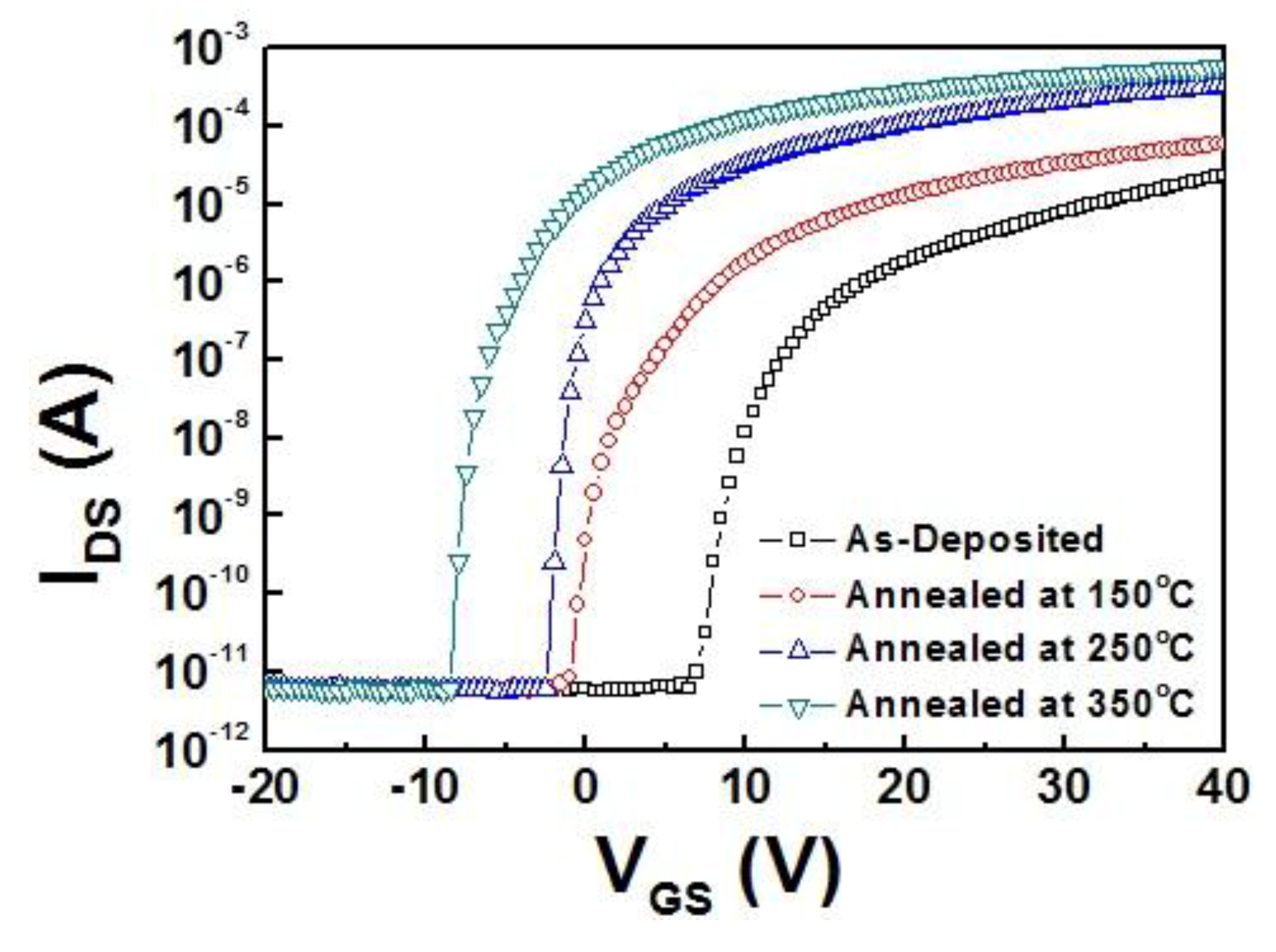
To investigate TFT device performance based on IZTO semiconductor channel layer, the transistor prepared using heavily-doped silicon wafer substrate was examined in n-channel mode. Figure 4 depicts the transfer characteristic of IZTO TFT device deposited by RF magnetron sputtering with annealing temperature variation. It is seen that field effect mobility (μFE), on/off current ratio (Ion/off), and subthreshold swing (SS) values improved as annealing temperature increased from 150 °C to 350 °C, as shown in Table 4. Threshold voltage (VT) value tended to shift to zero voltage by controlling the carrier concentration of IZTO channel layer with the increasing annealing temperature. As the carrier concentration increased, the threshold voltage and subthreshold swing values shifted to more desirable values [27,28]. The enhancement of TFT performance was noticed by lowering resistivity and reducing SS values of IZTO channel layer with increasing annealing temperature, which might be mainly due to oxygen diffusion from IZTO layer and rearrangement of molecular bonding during annealing process, thus inducing the acceleration of electrons to pass through channel region between source and drain [29].
Our TFT devices made from a zinc-rich IZTO channel layer demonstrated excellent performance with a field effect mobility value of 34 cm2/Vs, which is higher than the values reported by other research groups [24,30]. It is also noticed that interface defect concentration (NT) value, which was estimated from SS value, was reduced with increasing annealing temperature. It is obvious the mobility of charge carriers would then be improved as electrons travel from source to drain through the a-IZTO channel layer [19].
The stability of the a-IZTO thin film transistor annealed at 350 °C was explored under both positive bias stress (PBS) and negative bias stress (NBS). The tests were performed at drain voltage (VDS) of ±10 V with stress time of up to 1200 s. As shown in Figure 5, the transfer characteristics curve shifted to the positive direction, and thus threshold voltage also changed to the positive direction with the increase of bias stress time. This voltage shift of transfer characteristics was attributed to electron trapping at the gate/insulator interface in n-type TFTs [31]. The threshold voltage shift under PBS is about +1.9 V while the NBS is about +3.1 V. Higher bias instability of a-IZTO thin film transistor would be expected to decrease further by applying passivation layer to prevent humidity [32].
4. Summary and Conclusions
Room-temperature-deposited IZTO films remained uniform amorphous phase even after annealing at temperatures of up to 350 °C, indicating that the enhancement of TFT performance was not due to the crystallization of the IZTO layer. IZTO films deposited by RF magnetron sputtering showed transparency values higher than 84%, regardless of the annealing treatment across the visible light range, which is desirable for transparent electronic device applications. It was found that annealing treatment affected TFT parameters in such a way as to increase the carrier mobility and on/off current ratio, and to decrease the sub-threshold swing value. The threshold voltage value also shifted to the negative direction, and the carrier concentration value increased upon annealing. Interface defect concentration also reduced, resulting in the movement of more electrons without being trapped between the active layer and the source or drain electrode. However, stability improvement under bias stress still remains as an issue to enhance the performance of a-IZTO thin film transistors in the near future.
Acknowledgments
This study was supported by the National Research Foundation of Korea (Grant No. 2015R1A2A2A01006655).
Author Contributions
Imas Noviyana fabricated, measured and analyzed the data of the TFTs devices and wrote the paper, Annisa Dwi Lestari performed Hall measurement and processed experimental data, Maryane Putri contributed in suggestions for discussion, Mi-Sook Won and Jong-Seong Bae assisted with the interpreting XPS data, Young-Woo Heo and Hee Young Lee monitored and provided discussions and valuable suggestions.
Conflicts of Interest
The authors declare no conflict of interest.
References
- Nomura, K.; Ohta, H.; Takagi, A.; Kamiya, T.; Hirano, M.; Hosono, H. Room-temperature fabrication of transparent flexible thin-film transistors using amorphous oxide semiconductors. Nature 2004, 432, 488–492. [Google Scholar] [CrossRef] [PubMed]
- Staebler, D.L.; Wronski, C.R. Reversible conductivity changes in discharge-produced amorphous Si. Appl. Phys. Lett. 1977, 31, 292–294. [Google Scholar] [CrossRef]
- Jahinuzzaman, S.M.; Sultana, A.; Sakariya, K.; Servati, P.; Nathan, A. Threshold voltage instability of amorphous silicon thin-film transistors under constant current stress. Appl. Phys. Lett. 2005, 87, 023502. [Google Scholar] [CrossRef]
- Chang, T.S.; Chang, T.C.; Liu, P.T.; Tu, C.H.; Yeh, F.S. Improvement of hydrogenated amorphous-silicon TFT performance with low-k siloxane-based Hydrogen Silsesquioxane (HSQ) passivation layer. IEEE Electron Device Lett. 2006, 27, 902–904. [Google Scholar] [CrossRef]
- Karim, S.K.; Nathan, A.; Hack, M.; Milne, W.I. Drain-bias dependence of threshold voltage stability of amorphous silicon TFTs. IEEE Electron Device Lett. 2004, 25, 188–190. [Google Scholar] [CrossRef]
- Arai, T. Oxide-TFT technologies for next-generation AMOLED displays. J. Soc. Inf. Disp. 2012, 20, 156–161. [Google Scholar] [CrossRef]
- Chung, H.K.; Lee, K.Y.; Lee, S.T. Alternative approach to large-size AMOLED HDTV. J. Soc. Inf. Disp. 2006, 14, 49–55. [Google Scholar] [CrossRef]
- Hong, S.K.; Kim, B.K.; Ha, Y.M. LTPS technology for improving the uniformity of AMOLEDs. SID Symp. Dig. Tech. Pap. 2007, 38, 1366–1369. [Google Scholar] [CrossRef]
- Hayashi, R.; Sato, A.; Ofuji, M.; Abe, K.; Yabuta, H.; Sano, M.; Kumomi, H.; Nomura, K.; Kamiya, T.; Hirano, M.; et al. Improved amorphous In-Ga-Zn-O TFTs. SID Symp. Dig. Tech. Pap. 2008, 39, 621–624. [Google Scholar] [CrossRef]
- Park, S.H.K.; Hwang, C.S.; Cho, D.H.; Yoon, S.M.; Yang, S.; Byun, C.; Ryu, M.; Lee, J.I.; Kwon, O.; Cheong, W.S.; et al. Effect of channel/insulator interface formation process on the oxide TFT performance. SID Symp. Dig. Tech. Pap. 2009, 40, 276–279. [Google Scholar] [CrossRef]
- Caglar, Y.; Caglar, M.; Ilican, S.; Aksoy, S.; Yakuphanoglu, F. Effect of channel thickness on the field effect mobility ZnO-TFT fabricated by sol gel process. J. Alloy. Compd. 2015, 621, 189–193. [Google Scholar] [CrossRef]
- Fortunato, E.; Barquinha, P.; Pimintel, A.; Pereira, L.; Goncalves, G.; Martins, R. Amorphous IZO TTFTs with saturation mobilities exceeding 100 cm2/Vs−1. Phys. Status Solid 2007, 34, R34–R36. [Google Scholar] [CrossRef]
- Avis, C.; Jang, J. High-performance processed Oxide TFT with aluminum oxide gate dielectric fabricated by a sol-gel method. J. Mater. Chem. 2011, 21, 10649–10652. [Google Scholar] [CrossRef]
- Hoel, C.A.; Gaillard, J.F.; Poeppelmeier, K.R. Probing the local structure of crystalline ZITO: In2−2xSnxZnxO3 (x ≤ 0.4). Solid State Chem. 2010, 183, 761–768. [Google Scholar] [CrossRef]
- Putri, M.; Koo, C.Y.; Lee, J.A.; Kim, J.J.; Lee, H.Y. Transparent conducting indium zinc tin oxide thin films with low indium content deposited by radio frequency magnetron sputtering. Thin Solid Films 2014, 559, 44–48. [Google Scholar] [CrossRef]
- Damisih; Ma, H.C.; Kim, J.J.; Lee, H.Y. The electrical and optical properties of indium zinc tin oxide thin films with different Sn/Zn ratio. Thin Solid Films 2012, 520, 3741–3745. [Google Scholar] [CrossRef]
- Damisih; Ma, H.C.; Yoon, D.J.; Kim, D.J.; Lee, H.Y. Transparent conductive indium zinc tin oxide thin films for solar cell applications. J. Nanoelectron. Optoelectron. 2011, 6, 223–229. [Google Scholar] [CrossRef]
- Wagner, C.D.; Gale, L.H.; Raymond, R.H. Two-dimensional chemical state plots: A standardized data set for use in identifying chemical states by X-ray photoelectron spectroscopy. Anal. Chem. 1979, 51, 466–482. [Google Scholar] [CrossRef]
- Fuh, C.S.; Liu, P.T.; Huang, W.H. Effect of annealing on defect elimination for high mobility amorphous indium-zinc-tin-oxide thin-film transistor. IEEE Electron Device Lett. 2014, 35, 1103–1105. [Google Scholar] [CrossRef]
- Saji, K.J.; Jayaraj, M.K. Optical and electrical properties of co-sputtered amorphous transparent conducting zinc oxide thin films. Thin Solid Films 2008, 516, 6002–6007. [Google Scholar] [CrossRef]
- Hung, L.S.; Chen, C.H. Recent progress of molecular organic electroluminescent materials and devices. Mater. Sci. Eng. 2002, 39, 143–222. [Google Scholar] [CrossRef]
- Ow-Yang, C.W.; Yeom, H.Y.; Paine, D.C. Fabrication of transparent conducting amorphous Zn-Sn-In-O thin films by direct current magnetron sputtering. Thin Solid Films 2008, 516, 3105–3111. [Google Scholar] [CrossRef]
- Tauc, J.; Grigorovici, R.; Vancu, A. Optical properties and electronic structure of amorphous germanium. Phys. Status Solid 1966, 15, 627–637. [Google Scholar] [CrossRef]
- Kim, S.H.; Ahn, C.H.; Yun, M.G.; Cho, S.W.; Cho, H.K. Anomalous tin chemical bonding in indium-zinc-tin oxide films and their thin film transistor performance. J. Phys. D 2014, 47, 485101. [Google Scholar] [CrossRef]
- Nayak, P.K.; Hedhili, M.N.; Cha, D.; Alshareef, H.N. High performance In2O3 thin film transistors using chemically derived aluminum oxide dielectric. Appl. Phys. Lett. 2013, 103, 033518. [Google Scholar] [CrossRef]
- Kofstad, P. Defect reactions. In Nonstoichiometry, Diffusion and Electrical Conductivity in Binary Metal Oxides; Wiley Interscience: New York, NY, USA, 1972; Chapter 2. [Google Scholar]
- Kim, M.H.; Lee, H.S. Effect of in addition and annealing temperature on the device performance of solution-processed In-Zn-Sn-O thin film transistors. Solid-State Electron. 2014, 96, 14–18. [Google Scholar] [CrossRef]
- Bang, S.; Lee, S.; Park, J.; Park, S.; Jeong, W.; Jeon, H. Investigation of the effects of interface carrier concentration on ZnO thin film transistors fabricated by atomic layer deposition. J. Phys. D 2009, 42, 235102. [Google Scholar] [CrossRef]
- Nguyen, C.P.T.; Trinh, T.T.; Dao, V.A.; Raja, J.; Jang, K.; Le, T.A.H.; Iftiquar, S.M.; Yi, J. Bias-stress-induced threshold voltage shift dependence of negative charge trapping in the amorphous indium tin zinc oxide thin-film transistors. Semiconduct. Sci. Technol. 2013, 28, 105014. [Google Scholar] [CrossRef]
- Denny, Y.R.; Lee, K.; Seo, S.; Oh, S.K.; Kang, H.J.; Yang, D.S.; Heo, S.; Chung, J.C.; Lee, J.C. Electrical, electronic and optical properties of amorphous indium zinc tin oxide thin films. Appl. Surf. Sci. 2014, 315, 454–458. [Google Scholar] [CrossRef]
- Jun, T.; Song, K.; Jung, Y.; Jeong, S.; Moon, J. Bias stress stable aqueous solution derived Y-doped ZnO thin film transistors. J. Mater. Chem. 2011, 21, 13524–13529. [Google Scholar] [CrossRef]
- Olziersky, A.; Barquinha, P.; Vila, A.; Pereira, L.; Goncalves, G.; Fortunato, E.; Martins, R.; Morante, J.R. Insight on the SU-8 resist as passivation layer for transparent Ga2O3-In2O3-ZnO thin-film transistors. J. Appl. Phys. 2010, 108, 064505. [Google Scholar] [CrossRef]
Figure 1.
X-ray diffraction patterns of the indium zinc tin oxide (IZTO) films deposited at room temperature onto glass substrates at various annealing temperatures in the range of 150–350 °C.
Figure 1.
X-ray diffraction patterns of the indium zinc tin oxide (IZTO) films deposited at room temperature onto glass substrates at various annealing temperatures in the range of 150–350 °C.
Figure 2.
Optical properties of IZTO films deposited at room temperature onto glass substrates at various annealing temperatures in the range of 150–350 °C.
Figure 2.
Optical properties of IZTO films deposited at room temperature onto glass substrates at various annealing temperatures in the range of 150–350 °C.

Figure 3.
X-ray photoelectron spectroscopy (XPS) spectra of (a) detailed and (b) O 1s for IZTO films at various annealing temperatures in the range of 150–350°C. Metal-O: metal oxide; Oxy. Vac: oxygen vacancy.
Figure 3.
X-ray photoelectron spectroscopy (XPS) spectra of (a) detailed and (b) O 1s for IZTO films at various annealing temperatures in the range of 150–350°C. Metal-O: metal oxide; Oxy. Vac: oxygen vacancy.

Figure 4.
Transfer curve of IZTO thin film transistors deposited at various annealing temperatures in the range of 150–350 °C.
Figure 4.
Transfer curve of IZTO thin film transistors deposited at various annealing temperatures in the range of 150–350 °C.

Figure 5.
Transfer curves of amorphous IZTO (a-IZTO) thin film transistors annealed at 350 °C as a function of stress time under (a) positive bias stress (PBS) and (b) negative bias stress (NBS).
Figure 5.
Transfer curves of amorphous IZTO (a-IZTO) thin film transistors annealed at 350 °C as a function of stress time under (a) positive bias stress (PBS) and (b) negative bias stress (NBS).

Table 1.
Root-mean-square values of the IZTO films from atomic force microscopy (AFM) data.
| Annealing Temperature | Rq (nm) |
|---|---|
| As-Deposited | 0.21 |
| 150 °C | 0.31 |
| 250 °C | 0.23 |
| 350 °C | 0.33 |
Table 2.
Electrical property data of the IZTO thin films deposited by RF magnetron sputtering on glass substrates at various annealing temperatures in the range of 150–350 °C.
Table 2.
Electrical property data of the IZTO thin films deposited by RF magnetron sputtering on glass substrates at various annealing temperatures in the range of 150–350 °C.
| Annealing Temperature | Carrier Concentration (cm−3) | Resistivity (Ω·cm) |
|---|---|---|
| As-Deposited | 5.4 × 10¹⁶ | 10 |
| 150 °C | 6.7 × 10¹⁶ | 9.5 |
| 250 °C | 7.2 × 10¹⁷ | 0.60 |
| 350 °C | 1.0 × 10¹⁸ | 0.33 |
Table 3.
Relative peak area ratio and binding energy of the IZTO thin films deposited by RF magnetron sputtering on silicon substrates at various annealing temperatures in the range of 150–350 °C.
Table 3.
Relative peak area ratio and binding energy of the IZTO thin films deposited by RF magnetron sputtering on silicon substrates at various annealing temperatures in the range of 150–350 °C.
| Annealing Temperature | Binding Energy (eV) | Peak Area (%) | |||
|---|---|---|---|---|---|
| Metal-Oxide | O-OH | Oxy. Vac | Metal-Oxide | Oxy. Vac | |
| As-Deposited | 529.42 | 531.39 | 530.40 | 82 | 18 |
| 150 °C | 529.28 | 531.33 | 530.40 | 77 | 23 |
| 250 °C | 529.32 | 531.34 | 530.40 | 75.8 | 24.2 |
| 350 °C | 529.31 | 531.39 | 530.40 | 71.2 | 28.8 |
Table 4.
Summary of transistor parameters of IZTO thin film transistors (TFTs) deposited by RF magnetron sputtering at various annealing temperatures in the range of 150–350 °C.
Table 4.
Summary of transistor parameters of IZTO thin film transistors (TFTs) deposited by RF magnetron sputtering at various annealing temperatures in the range of 150–350 °C.
| Annealing Temperature | µFE (cm2/Vs) | Ion/off (A) | VT (V) | SS (V/dec) | NT (cm−2) |
|---|---|---|---|---|---|
| As-Deposited | 2.5 | ~106 | 18.6 | 1.22 | 2.1 × 10¹² |
| 150 °C | 4.0 | ~107 | 4.6 | 0.38 | 5.8 × 10¹¹ |
| 250 °C | 14 | ~107 | −0.8 | 0.15 | 1.6 × 10¹¹ |
| 350 °C | 34 | ~108 | −4.6 | 0.12 | 1.1 × 10¹¹ |
© 2017 by the authors. Licensee MDPI, Basel, Switzerland. This article is an open access article distributed under the terms and conditions of the Creative Commons Attribution (CC BY) license (http://creativecommons.org/licenses/by/4.0/).
Share and Cite
MDPI and ACS Style
Noviyana, I.; Lestari, A.D.; Putri, M.; Won, M.-S.; Bae, J.-S.; Heo, Y.-W.; Lee, H.Y. High Mobility Thin Film Transistors Based on Amorphous Indium Zinc Tin Oxide. Materials 2017, 10, 702. https://doi.org/10.3390/ma10070702
AMA Style
Noviyana I, Lestari AD, Putri M, Won M-S, Bae J-S, Heo Y-W, Lee HY. High Mobility Thin Film Transistors Based on Amorphous Indium Zinc Tin Oxide. Materials. 2017; 10(7):702. https://doi.org/10.3390/ma10070702
Chicago/Turabian StyleNoviyana, Imas, Annisa Dwi Lestari, Maryane Putri, Mi-Sook Won, Jong-Seong Bae, Young-Woo Heo, and Hee Young Lee. 2017. "High Mobility Thin Film Transistors Based on Amorphous Indium Zinc Tin Oxide" Materials 10, no. 7: 702. https://doi.org/10.3390/ma10070702
Note that from the first issue of 2016, this journal uses article numbers instead of page numbers. See further details here.