Sol-Gel Derived Active Material for Yb Thin-Disk Lasers


Centro de Química Estrutural/DEQ, Instituto Superior Técnico, Universidade de Lisboa, Av. Rovisco Pais, 1049-001 Lisboa, Portugal
*
Authors to whom correspondence should be addressed.
Materials 2017, 10(9), 1020; https://doi.org/10.3390/ma10091020
Submission received: 27 July 2017
/
Revised: 28 August 2017
/
Accepted: 28 August 2017
/
Published: 2 September 2017
(This article belongs to the Special Issue Sol-Gel Chemistry Applied to Materials Science)
Abstract
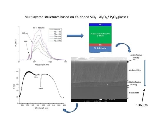
:A ytterbium doped active material for thin-disk laser was developed based on aluminosilicate and phosphosilicate glass matrices containing up to 30 mol% YbO1.5. Thick films and bulk samples were prepared by sol-gel processing. The structural nature of the base material was assessed by X-ray diffraction and Raman spectroscopy and the film morphology was evidenced by scanning electron microscopy. The photoluminescence (PL) properties of different compositions, including emission spectra and lifetimes, were also studied. Er3+ was used as an internal reference to compare the intensities of the Yb3+ PL peaks at ~ 1020 nm. The Yb3+ PL lifetimes were found to vary between 1.0 and 0.5 ms when the Yb concentration increased from 3 to 30 mol%. Based on a figure of merit, the best active material selected was the aluminosilicate glass composition 71 SiO2-14 AlO1.5-15 YbO1.5 (in mol%). An active disk, ~ 36 μm thick, consisting of a Bragg mirror, an aluminosilicate layer doped with 15 mol% Yb and an anti-reflective coating, was fabricated.
1. Introduction
The use of laser technology in industrial and scientific applications is widely spread, given its added value in tasks such as welding, cutting or marking, where the speed and quality of the laser beam are determinant, thus influencing the competitiveness of the industry. Among the various types of lasers currently available, dielectric solid state lasers play an important role due mainly to the beam quality. They normally use a crystalline material as the lasing medium and, contrarily to semiconductor diode lasers, they are usually optically pumped. Fiber and disk lasers, in particular Yb3+-doped ones, such as Yb:YAG, present high average output power, excellent beam quality and high efficiency [1,2]. Due to their unique features, thin-disk lasers are one of the best laser solutions for material micro-processing in automotive, aerospace, and heavy industry, with laser powers of up to 16 kW and beam qualities ≥2 mm·mrad [3], or for military applications as recently demonstrated by Boeing, where more than 30 kW power was attained [4].
The thin-disk laser concept was developed by Adolf Giesen et al. [5], who used a thin laser crystal disc with one face mounted on a water cooled block. The use of a very small thickness of active material (~100–200 µm), corresponding to a high surface area to volume ratio, leads not only to superior beam quality, but also to highly efficient cooling, resulting in almost negligible thermal gradients. Moreover, the residual gradient is symmetrical, which also contributes to an optimal beam quality. However, the small thickness of the active material results in an insufficient absorption length that must be compensated by a multi-pass pumping scheme [6]. The gain medium is typically a thin disk of Yb:YAG crystal grown by the Czochralski method, or another ytterbium-doped medium such as Yb:Lu3Al5O12 or Yb:Lu2O3 [7,8], with a highly reflective coating on one side and an anti-reflective coating on the other side. The advantages of Yb-doped active material include the simple electronic structure of Yb3+, with only one excited state level (2F5/2) with a lifetime of the order of 1–2 ms and ~10,000 cm−1 above the ground state (2F7/2), therefore with low non-radiative decay rates in most solid matrices and the possibility of achieving high doping levels without excessive luminescence quenching [9]. However, cutting such a small crystal thickness presents problems that could be overcome with a different approach: the active medium could be prepared by sol-gel (SG) processing. This is a relatively cheap wet chemistry technique which involves the hydrolysis and condensation of precursor species like organometallic compounds and nitrates in the presence of a catalyst, forming a porous gel structure that can be densified by subsequent heat treatment. Thick films can be doped with different concentrations of an active species like Yb and deposited on an appropriate substrate, e.g., a single crystal Si wafer. Moreover, anti-reflective and highly reflective coatings can be obtained as 1-D Photonic Bandgap Structures (PBGs), or photonic crystals (PCs), which are multilayered structures at the optical nanoscale that control the propagation of light, including the inhibition or enhancement of spontaneous emission (SE) of light at certain wavelengths [10,11]. Such structures may be deposited with high optical quality by the SG process [12].
Recently, our research group obtained polycrystalline Yb:YAG ceramic films as well as Yb-doped silicate glass films by the sol-gel process, with potential application as the active material in thin-disk lasers [13,14]. In the present work, multilayered structures based on Yb-doped SiO2-Al2O3 or SiO2-P2O5 oxide glass matrices were investigated and active films prepared; the purpose of the addition of Al or P to the silica matrix was to create non-bridging oxygen species to help disperse the Yb3+ ions homogeneously in the glass network, reducing possible concentration quenching phenomena.
2. Results
2.1. X-Ray Diffraction
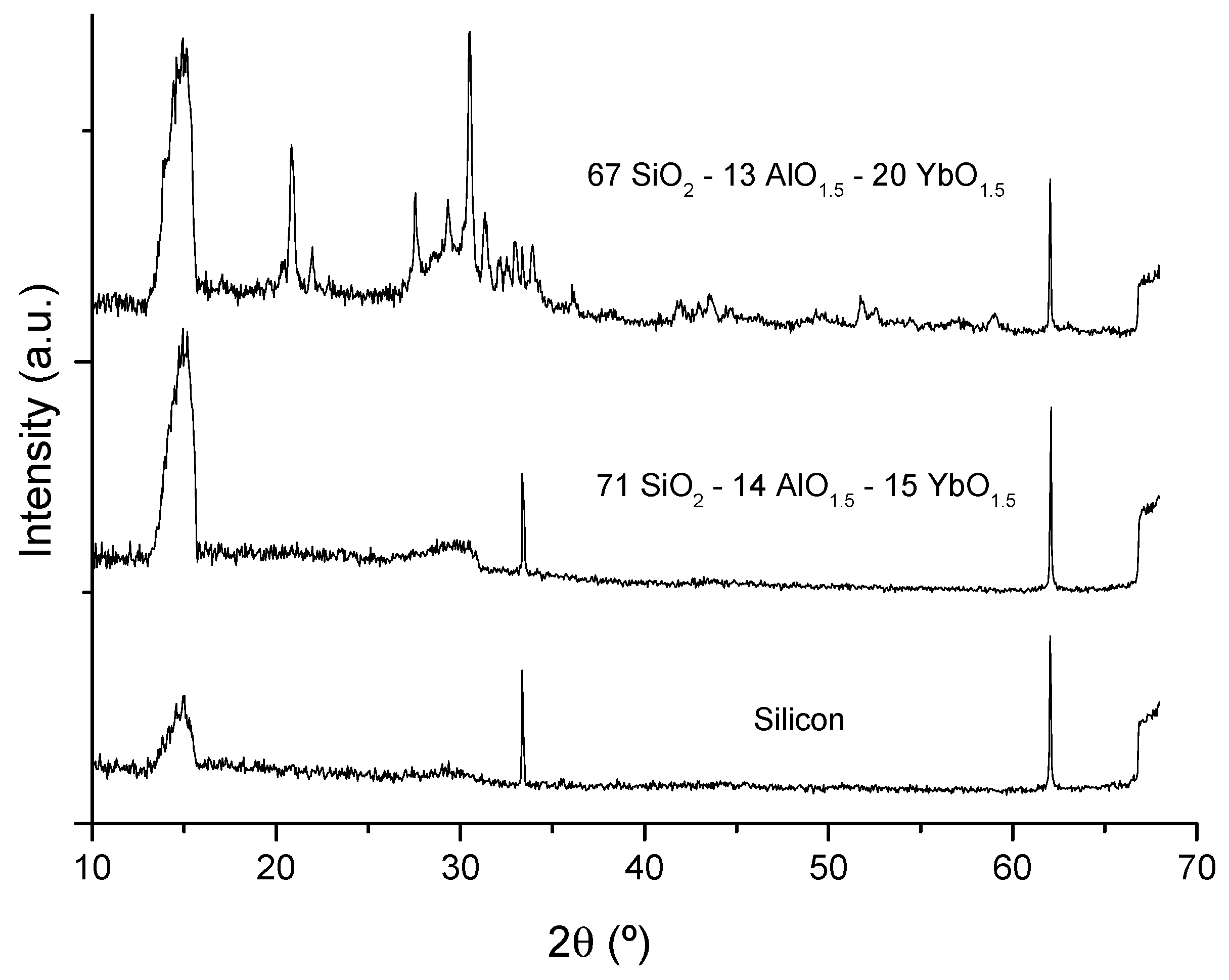
In order to avoid the presence of scattering centers, it is important to determine whether the heat treatments of the bulk samples (up to ~1050 °C) or the films (up to ~1100 °C) may cause any crystallization. The difference in the temperatures used was due to the fact that multilayer films are treated sequentially, with fast heating from room temperature to the final heat treatment temperature, while bulk samples are monolithic and slowly heated until the final temperature, in order to allow complete combustion of the organic residues. For this purpose, both films and powdered bulk samples were analyzed by XRD. Figure 1 includes the XRD patterns of four aluminosilicate bulk samples, showing the amorphous nature of the aluminosilicates up to 15 mol% YbO1.5, whereas higher Yb concentrations led to partial crystallization, namely of the Yb2Si2O7 phase. The same behavior had already been observed for phosphosilicate glass films, where partial crystallization occurred for compositions with more than 5 mol% YbO1.5, as reported in [14]. Figure 2 shows the X-ray diffraction (XRD) patterns of Yb-doped aluminosilicate films plus a silicon wafer reference, where partial crystallization is also observed for the 20 mol% YbO1.5 film, while the amorphous character of a film with 15 mol% YbO1.5 is confirmed. The patterns are truncated at 2θ = 68°, due to the main Si peak at 69.2°, corresponding to the {400} planes.
2.2. Raman Spectroscopy
Figure 3 shows the Raman spectra of the heat treated Yb-doped aluminosilicate bulk glass samples. The Raman spectra, up to 15 mol% ytterbia, are relatively similar to that of pure vitreous silica, with the growth of a peak near 940 cm−1 with increasing Yb concentrations, probably due to the formation of Si-O– non-bridging oxygen bonds with the Yb3+ ions, rather than Si-O-Al sequences as previously assigned [14], since there is no correlation with the alumina content, which remains practically constant. For heat treated aluminosilicate compositions with higher Yb contents, the appearance of several sharp peaks suggests the formation of one or more crystalline phases, in agreement with the XRD results. However, this behavior depends also on the heat treatment temperature, as observed for the 71 SiO2-14 AlO1.5-15 YbO1.5 samples, where an increase of 50 °C is sufficient to promote significant crystallization for this composition.
2.3. Fourier Transform Infrared (FTIR) Spectroscopy
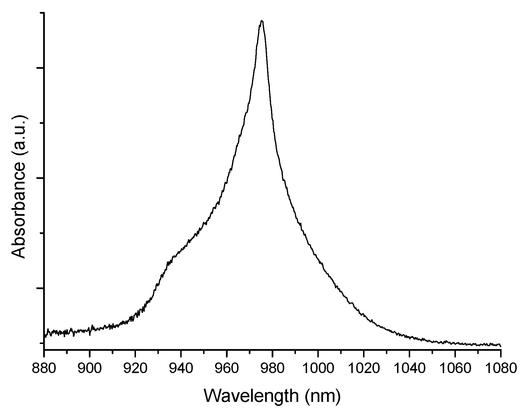
Yb3+ ion absorption was measured in the near infrared (NIR), for both aluminosilicate and phosphosilicate monolithic gels. The Yb3+ ion is known to absorb at wavelengths near ~975 nm, due to the 2F7/2 → 2F5/2 transition starting from the ground state, with a shoulder near ~940 nm [14]. Figure 4 shows the Yb3+ absorption spectrum for the 79 SiO2-16 AlO1.5-5 YbO1.5 bulk gel sample, before heat treatment, when it was still monolithic and transparent.
2.4. Photoluminescence Spectroscopy
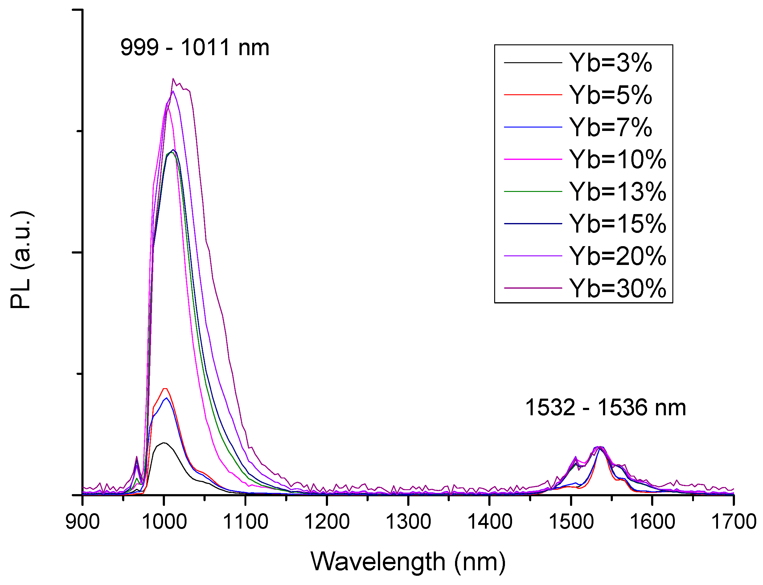
Figure 5 and Figure 6 show the photoluminescence (PL) spectra of bulk Yb/Er co-doped phosphosilicate and aluminosilicate-matrix samples, respectively. The spectra have been normalized to the intensity of the Er3+ peak emission at 1532 nm. Erbium was used here as an internal reference [13,14] and its concentration, the same in all cases (0.002 mol% Er), was kept to a minimum in order to avoid any significant Yb3+ → Er3+ energy transfer through the so-called “antenna effect”.
In Figure 5, two main peaks can be observed for the phosphosilicate glasses at 999–1011 and 1532 nm, representing Yb3+ and Er3+ PL emissions due to 2F5/2 → 2F7/2 and 4I13/2 → 4I15/2, respectively. The Yb3+ PL peak position varied with the Yb content between 999 nm (for 3 mol% Yb) and 1011 nm (for 30 mol% YbO1.5). The normalization at 1532 nm revealed a general increase in the PL peak intensity with increasing Yb content. A residual peak is also observed at 970 nm, due to the incompletely filtered excitation laser light.
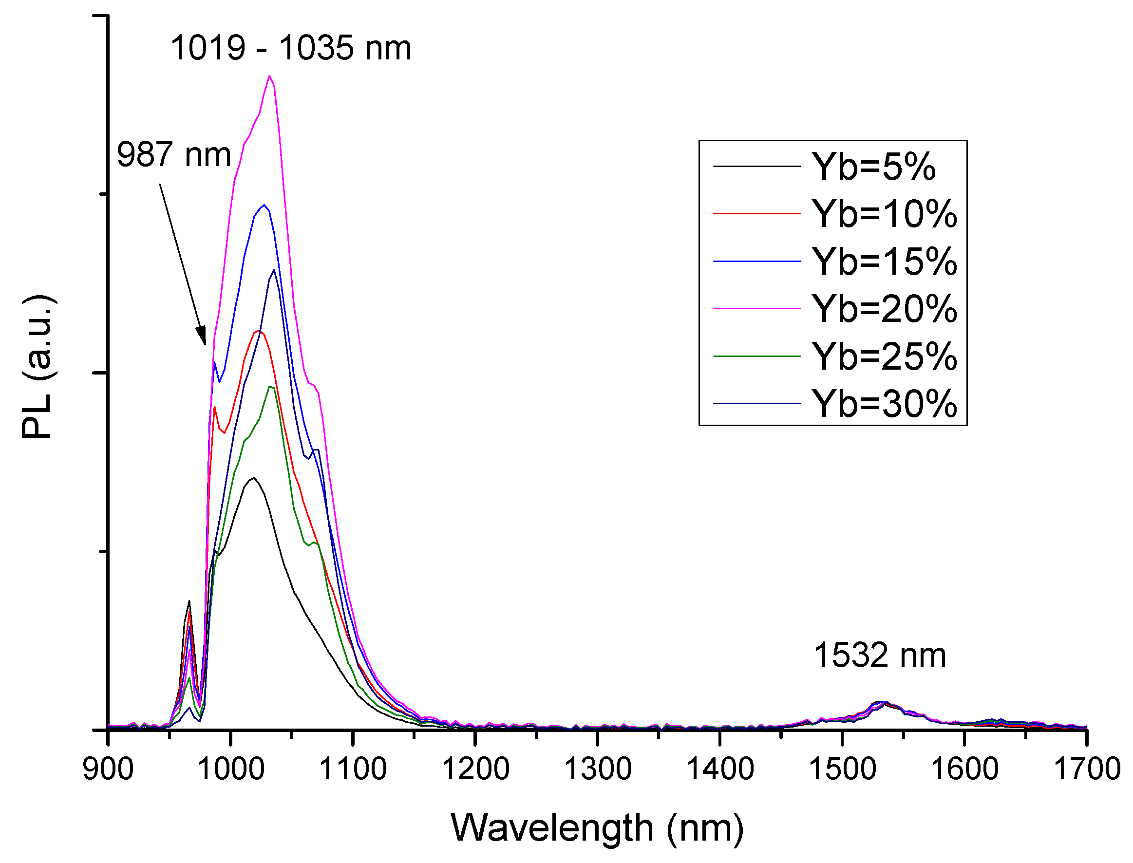
In Figure 6, the main emission peak of Yb-doped aluminosilicate glasses is located between 1019 and 1035 nm and its intensity increased for Yb contents up to 20 mol%, whereas it decreased for concentrations above that. An additional Yb3+ emission peak can be observed at 987 nm, which was not resolved in the phosphosilicate glass spectra of Figure 5.
The Yb3+:2F5/2 metastable level lifetimes were also measured for the phosphosilicate and aluminosilicate compositions. The PL decay curves had single exponential behavior as a function of time, t, as shown by the logarithmic plots of Figure 7 for aluminosilicate bulk glass samples doped with 5–30 mol% YbO1.5. The corresponding 1/e lifetime, τ, was found to vary between 1043 and 542 μs for phosphosilicates and between 624 and 482 μs for aluminosilicates, as shown in Table 1 and Table 2, respectively.
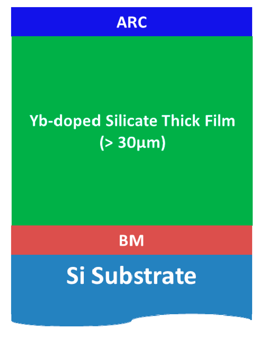
2.5. Active Disk
The active disk may consist of a thin disk (or thick film) of Yb-doped material, sandwiched between a highly reflective coating or Bragg Mirror (BM) and an anti-reflective coating (ARC). The characteristics of the BM, the ARC and active disk were all simulated and designed using the Transfer Matrix Method (TMM) software, developed in our group [11].
The high-reflective coatings, or BMs, were prepared by depositing seven pairs of low/high index layers of aluminosilicate glass (AS) and titania (T), respectively, directly onto the Si substrate. The molar composition 90 SiO2-10 AlO1.5 was chosen for the low-index AS material, based on previously developed 91 SiO2-9 AlO1.5 similar compositions [11]. Next, a thick Yb-doped aluminosilicate glass film with the optimized composition (71 SiO2-14 AlO1.5-15 YbO1.5) was deposited, followed by a photonic structure with anti-reflective properties at the top of the active disk. A small number of layers were used for this ARC, in order to avoid damaging the previously deposited Yb-doped multilayer disk through the additional heat treatment routines. The final ARC structure prepared consisted of three layers only (AS/T/AS) deposited on top of the Yb-doped active disk.
2.5.1. TMM Simulations
TMM simulations allowed the calculation of the transmission and reflection of a multilayer structure within a given wavelength range, based on the thickness and refractive index of each individual layer. Such simulations were performed in order to optimize both the BM and ARC, in terms of the number of low/high index pairs and individual layer thickness. The optimized BM consisted of seven pairs of AS (90 SiO2-10 AlO1.5)/T (TiO2) layers. The basic criterion is the “quarter-wave” condition Equation (1) for the optical thickness of each layer (equal to the product of the physical thickness, x and the refractive index, n) for a peak wavelength λ. The thickness of the AS (low index, n = 1.46) and T (high index, n = 2.22) layers were 175 and 115 nm, respectively, for a BM stop band with a center wavelength λ = 1020 nm (near the Yb3+ PL emission maximum), according to:
The ARC, on the other hand, designed for optimum anti-reflectivity at a pumping wavelength of 940 nm, was formed by a 42 nm titania layer sandwiched between two 180 nm aluminosilicate glass layers, whose thickness values (not “quarter-wave”) were obtained from TMM simulations by trial and error.
Figure 8 compares a BM reflectance measurement with its TMM simulation, while Figure 9 compares the transmission of the ARC with the corresponding TMM simulation. In the former case, high reflectivity is observed at both the 940 nm and the 1020 nm wavelengths; the observed values were slightly higher than 100%, since the BM reflected more than the Al mirror used as reference. In the latter case, the transmission is near 100%, evidencing the ARC properties and the interference fringes are due to the ARC thickness the agreement between theory and experiment appears reasonably good in both cases.
2.5.2. Active Disk Structure
An active disk doped with 15 mol% YbO1.5, whose structure consisted of a 7-pair BM, an active layer with molar composition 71 SiO2-14 AlO1.5-15 YbO1.5 and a 3-layer ARC, deposited on single-crystal silicon, was observed by scanning electron microscopy (SEM) and Figure 10 shows the corresponding cross-sectional image. This active disk had an overall thickness of ~10 μm. In the highly reflective portion, it is possible to distinguish the individual BM layers, for a total of seven high/low index pairs. In addition, the fracture surface of the Yb-doped portion is typical of an amorphous material, without any visible grains at this magnification.
2.5.3. Active Disk Properties
Figure 11 shows the XRD patterns of a ~36 μm active disk, deposited on silicon, where there is no evidence of any residual crystalline material.
The reflectance of the same active disk was measured in the NIR region (Figure 12) and a broad stop band of high reflectivity is visible over the range of ~750–1200 nm, due to the BM. A reflection-absorption effect is also observed at ~900–1000 nm, due to the Yb3+ absorption within the active layer.
The PL spectrum of the active disk is presented in Figure 13, which clearly shows the 987 nm and the major Yb3+ PL emission peaks, in addition to the residual excitation laser line.
3. Discussion
The SG method used in the present work enables the synthesis of the active material for an Yb-doped thin-disk laser through spin-coating deposition of disk-like films more than 30 μm thick. While the nature of the Yb-doped material was assessed by XRD plus FTIR and Raman spectroscopies, the morphology of the multilayer films and their optical quality were determined based on SEM analysis. The PL emission spectra and Yb3+ metastable level lifetimes of the doped material were also studied in detail.
XRD and Raman data indicate the amorphous nature of these aluminosilicate bulk samples and films with up to 15 mol% Yb, reveal a partially crystalline nature for 20 to 30 mol% Yb. However, an increase of the final heat treatment temperature of the bulk glasses from 1050 to 1100 °C is enough to promote some crystallization in the composition with 15 mol% Yb. Therefore, the Yb content, the glass matrix, and the heat treatment conditions are critical for the amorphous character of the samples. In fact, while aluminosilicate compositions remain amorphous for up to 15 mol% Yb, the phosphosilicates become partially crystallized with just 5 mol% Yb [14], revealing the different capabilities of Al and P to disperse the Yb3+ ions in the matrix, since the pentavalent P is less easily incorporated in the silicate glass structure compared to Al, which readily substitutes for Si.
The PL emission peaks at 987 and 1019–1035 nm correspond to transitions between the Stark levels of the 2F5/2 excited state and the 2F7/2 ground state of Yb3+: the sharp peak at 987 nm corresponds to the transition 5 → 1, between the lowest Stark levels of each J-manifold, whereas the intense peak at 1019–1035 nm is attributed to longer wavelength transitions from level 5 to higher lying Stark levels of the ground state, followed by thermalization to the lower J-level [15], without well resolved Stark splitting due to the amorphous nature of the host matrix. The continuous decrease of the measured PL lifetime with increasing Yb content, especially in the case of the phosphosilicate glass matrix (Table 1), indicates the occurrence of concentration quenching phenomena. This effect was already observed in previous studies [14,16,17], involving non-radiative energy transfer phenomena between closely spaced Yb3+ ions, despite the common assumption that the simple electronic energy level structure of Yb3+ excludes Excited State Absorption and a variety of quenching processes [18]. While the PL spectra (Figure 5 and Figure 6) refer to Yb/Er co-doped samples, the lifetime values were measured in Yb-doped samples without Er, to avoid any possible influence of Yb3+ → Er3+ energy transfer phenomena on the measured lifetimes. It is important to add that most samples were in the form of small plates, a few millimeters on the sides and a fraction of a mm thick. Since this area was still much larger than the laser spot size (typically of the order of ~0.5 mm), we did not observe any size effects. We also did not consider the possibility of self-absorption and photon trapping phenomena of the type reported by Mattarelli et al. [19] and Koughia and Kasap [20], given the fact that the samples were opaque and quite thin.
The potential performance of the present Yb-doped sol-gel thick films as thin-disk laser materials was evaluated based on the PL results, through a figure of merit (FOM) defined as the στ product between the normalized spontaneous emission cross section σ, taken as the ratio of Yb3+ (1000–1035 nm)/Er3+ (1532 nm) PL peak intensities and the corresponding 2F5/2 metastable level lifetime, τ. Table 1 and Table 2 indicate that the aluminosilicate composition 67 SiO2-13 AlO1.5-20 YbO1.5 had the highest FOM. However, XRD data (Figure 1 and Figure 2) show the occurrence of some incipient crystallization in this material. Therefore, the aluminosilicate composition 71 SiO2-14 AlO1.5-15 YbO1.5, which is completely amorphous and had the second highest FOM value, is chosen as the best composition for the doped film portion of the active disk. It is expected that an FOM based on stimulated emission cross-sections would lead to a similar conclusion.
4. Materials and Methods
4.1. Sample Preparation
Heavily Yb-doped aluminosilicate and phosphosilicate glass films and monoliths were prepared by the acid (HCl) catalyzed SG method, with the compositions shown in Table 3, where the aluminosilicate and phosphosilicate matrices had Si:Al and Si:P molar ratios approximately constant and equal to ~5:1 in both cases in order to keep a similar starting glass matrix structure, while the YbO1.5 content varied between 3 and 30 mol% on a cation basis. A small quantity of Er (0.002 mol%) was added as an internal reference for the PL measurements [13,14]. The precursors used for silica, phosphorus oxide, alumina, ytterbia, and erbia were tetraethyl orthosilicate (Alfa Aesar, Karlsruhe, Germany, 98%), P2O5 (Sigma-Aldrich Gmbh, Munich, Germany, ≥98%), aluminium nitrate nonahydrate (Alfa Aesar, Karlsruhe, Germany, 98%–102%), ytterbium nitrate pentahydrate (Strem Chemicals, Bischheim, France, 99.9%) and erbium nitrate pentahydrate (Aldrich Chemical Co., Inc., Milwaukee, WI, USA, 99.9%), respectively. Processing details for these materials are given elsewhere [14]. Titania films, used as high index material in the photonic bandgap (PBG) structures, were also synthetized by the SG method, using titanium (IV) isopropoxide (TiPOT) (Alfa Aesar, Karlsruhe, Germany, ≥97%) as precursor. Acid catalysis was also used here, through the mixing of glacial acetic acid (GAA), (Merck, Darmstadt, Germany, 100%) with TiPOT and stirring at room temperature over 1 h. After mixing, ethanol (Merck, ≥99.5%) was added slowly and the titania solution was stirred at room temperature for an additional hour.
4.1.1. Bulk Sample Preparation
Transparent silicate glass monoliths were obtained by aging the final SG solution for several days in an open container, followed by a heat-treatment of the obtained gel up to 1050 °C at a rate of 0.5 °C/min and slow cooling inside the furnace. During the heat treatment, most samples crumbled into a powder.
4.1.2. Film Deposition
Silicate or titania precursor solutions were aged for at least 24 h and 3 h, respectively, in a closed container and they were then spin-coated onto single crystal Si wafer substrates, at 2000 rpm for 30 s, using a Chemat KW-4A spin-coater. For thick multilayer deposition, each individual layer was heat treated at 1100 °C for 30 s in a muffle furnace.
4.1.3. Active Disk Preparation
In a Yb thin-disk laser, the active element may consist of a thin disk (or thick film) of Yb-doped material, sandwiched between a highly reflective coating or Bragg Mirror with peak reflectance at the signal wavelength (~1020 nm) and an anti-reflective coating with lowest reflectance at the pump wavelength (usually ~940 nm). When prepared by SG, the active disk will be a multilayered structure formed by several individual layers deposited in sequence according to the scheme shown in Figure 14.
4.2. Sample Characterization
Bulk powdered samples and thick films were analyzed by X-ray diffraction (XRD) with a Philips PW3020 powder diffractometer, at room temperature, using Cu Kα radiation (λ = 1.541874 Å) generated at 40 kV and 30 mA, in the 2θ range of 10°–90°, with a step of 3°/min. The average crystal size was estimated by X-ray line broadening, using the Scherrer formula [21] and taking into account the instrumental broadening.
Surface and cross-section images of active disk samples were obtained by Scanning Electron Microscopy (SEM) using a 7001F FEG-SEM (JEOL, Zaventem, Belgium) in secondary and/or back-scattered electron modes, at 15 kV. A ~15 nm layer of chromium was deposited onto the film samples, in order to promote the electrical conductivity at the surface of the insulating materials under observation.
A Nicolet 5700 FT-IR spectrometer (Thermo Electron Corporation, Madison, WI, USA) was used to record near infrared spectra, at a resolution of 4 cm−1. The 975 nm Yb3+ absorption peak was recorded in the NIR, in transmission, for transparent glass monolithic samples and in reflection mode, for highly reflective and ARC layers deposited on silicon wafers.
Raman spectra were collected with a LabRam HR 800 Evolution confocal micro-Raman spectrometer (Horiba, Villeneuve d’Ascq, France). The measurements were carried out with 532 nm laser excitation, using a 600 gr/mm grating and 100× objective lens. The incident laser power on the samples was ~10 mW and the spot diameter was ~1 µm.
The PL of Yb-doped silicate materials was excited with a 970 nm laser (Lumics High Power Module), using 3 W power and a filter to block the laser radiation. The emitted light was analyzed by an Avaspec-NIR256-1.7 fiber-optic spectrometer (Avantes, Apeldoorn, The Netherlands), at a resolution of 4 nm. The Yb3+ PL lifetimes were measured for chopped light with a PM3370B 60 MHz digital oscilloscope (Fluke, Eindhoven, The Netherlands).
5. Conclusions
A Ytterbium-doped active material for a thin-disk laser was developed using sol-gel processing. Ytterbium doped aluminosilicate and phosphosilicate glass matrices were investigated with a doping level between 3 and 30 mol% YbO1.5. Films with a thickness up to ~36 μm were prepared by spin-coating and bulk samples were obtained by sol-gel processing as well. The amorphous nature of the materials prepared was assessed by XRD and Raman spectroscopy, with some incipient crystallization observed in aluminosilicate samples with ≥20 mol% Yb and in phosphosilicate samples with ≥5 mol% Yb. The PL properties of Yb3+ were measured, with lifetime values between 1.0 and 0.5 ms when the Yb concentration increased from 3 to 30 mol%, with a concentration quenching effect for >3 mol% Yb. The Yb3+ PL intensities at λ ~1 μm, normalized to that of Er3+ internal standard at ~1.5 μm, together with the lifetime values, were combined in an FOM which led to the selection of the 71 SiO2-14 AlO1.5-15 YbO1.5 composition (mol%) as the best material for the active layer. An active disk ~36 μm thick, with a structure consisting of a Bragg mirror, an aluminosilicate layer doped with 15 mol% Yb and an anti-reflective coating was fabricated.
Acknowledgments
We gratefully acknowledge the “Fundação para a Ciência e a Tecnologia (FCT)”, for financial support under contract UID/QUI00100/2013. We would also like to thank ANI for support under project Multilaser (QREN project (SI I & DT) NO. 30179 (2013) and Paulo Morais for useful discussions.
Author Contributions
The samples were prepared by Tiago Ribeiro. Characterization of the samples was performed by Tiago Ribeiro, Rui M. Almeida and Luís F. Santos. The manuscript was written by Tiago Ribeiro, Rui M. Almeida and Luís F. Santos, and approved by all authors. All authors contributed to discussions and reviewed the manuscript.
Conflicts of Interest
The authors declare no conflict of interest.
References
- Heckl, O.H.; Kleinbauer, J.; Bauer, D.; Weiler, S.; Metzger, T.; Sutter, D.H. Ultrafast Thin-Disk Lasers. In Ultrashort Pulse Laser Technology—Laser Sources and Applications; Nolte, S., Schrempel, F., Dausinger, F., Eds.; Springer International Publishing AG: Cham, Switzerland, 2016; Volume 195, pp. 93–115. ISBN 978-3-319-17659-8. [Google Scholar]
- Giesen, A.; Speiser, J. Fifteen Years of Work on Thin-Disk Lasers: Results and Scaling Laws. IEEE J. Sel. Top. Quantum Electron. 2007, 13, 598–609. [Google Scholar] [CrossRef]
- TRUMPF. Disk Lasers. Available online: http://www.trumpf-laser.com/en/products/solid-state-lasers/disk-lasers.html (accessed on 5 July 2017).
- BOEING. Boeing Thin Disk Laser Exceeds Performance Requirements During Testing. Available online: http://boeing.mediaroom.com/Boeing-Thin-Disk-Laser-Exceeds-Performance-Requirements-During-Testing (accessed on 5 July 2017).
- Giesen, A.; Hugel, H.; Voss, A.; Wittig, K.; Brauch, U.; Opower, H. Scalable concept for diode-pumped high-power solid-state lasers. Appl. Phys. B 1994, 58, 365–372. [Google Scholar] [CrossRef]
- Huang, Y.; Zhu, X.; Zhu, G.; Shang, J.; Wang, H.; Qi, L.; Zhu, C.; Guo, F. A multi-pass pumping scheme for thin disk lasers with good anti-disturbance ability. Opt. Express 2015, 23, 4605–4613. [Google Scholar] [CrossRef] [PubMed]
- Marchese, S.V.; Baer, C.R.E.; Peters, R.; Kränkel, C.; Engqvist, A.G.; Golling, M.; Maas, D.J.H.C.; Petermann, K.; Südmeyer, T.; Huber, G.; et al. Efficient femtosecond high power Yb:Lu2O3 thin disk laser. Opt. Express 2007, 15, 16966–16971. [Google Scholar] [CrossRef] [PubMed]
- Peters, R.; Kränkel, C.; Petermann, K.; Huber, G. Broadly tunable high-power Yb:Lu2O3 thin disk laser with 80% slope efficiency. Opt. Express 2007, 15, 7075–7082. [Google Scholar] [CrossRef]
- Francini, R.; Giovenale, F.; Grassano, U.M.; Laporta, P.; Taccheo, S. Spectroscopy of Er and Er-Yb-doped phosphate glasses. Opt. Mater. 2000, 13, 417–425. [Google Scholar] [CrossRef]
- Marques, A.C.; Almeida, R.M. Rare earth-doped photonic crystals via sol-gel. J. Mater. Sci. Mater. Electron. 2009, 20, 307–311. [Google Scholar] [CrossRef]
- Li, Y.G.; Almeida, R.M. Simultaneous broadening and enhancement of the 1.5 micron photoluminescence peak of Er3+ ions embedded in a 1-D photonic crystal microcavity. Appl. Phys. B 2010, 98, 809–814. [Google Scholar] [CrossRef]
- Li, Y.G.; Almeida, R.M. Elimination of porosity in heavily rare-earth doped sol–gel derived silicate glass films. J. Sol-Gel Sci. Technol. 2012, 61, 332–339. [Google Scholar] [CrossRef]
- Ferreira, J.; Santos, L.F.; Almeida, R.M. Sol-gel derived Yb:YAG polycrystalline ceramics for laser applications. J. Sol-Gel Sci. Technol. 2017, 83, 436–446. [Google Scholar] [CrossRef]
- Ribeiro, T.V.; Santos, L.F.; Gonçalves, M.C.; Almeida, R.M. Heavily Yb-doped silicate glass thick films. J. Sol-Gel Sci. Technol. 2017, 81, 105–113. [Google Scholar] [CrossRef]
- Perumal, R.N.; Subalakshmi, G. Near-infrared down-conversion in Yb3+:TiO2 for solar cell applications. J. Mater. Sci. Mater. Electron. 2017. [Google Scholar] [CrossRef]
- Paschotta, R.; Nilsson, J.; Barber, P.R.; Caplen, J.E.; Tropper, A.C.; Hanna, D.C. Lifetime quenching in Yb-doped fibers. Opt. Commun. 1997, 136, 375–378. [Google Scholar] [CrossRef]
- Malinoski, M.; Kaczkan, M.; Piramidowicz, R.; Frukacz, Z.; Sarnecki, J. Cooperative emission in Yb3+: YAG planar epitaxial waveguides. J. Lumin. 2011, 94–95, 29–33. [Google Scholar] [CrossRef]
- RP Photonics Encyclopedia. Available online: http://www.rp-photonics.com/ytterbium_doped_gain_media.html (accessed on 5 July 2017).
- Matarrelli, M.; Montagna, M.; Zampedri, L.; Chiasera, A.; Ferrari, M.; Righini, G.C.; Fortes, L.M.; Gonçalves, M.C.; Santos, L.F.; Almeida, R.M. Self-absorption and Radiation trapping in Er3+-doped TeO2-based glasses. Europhys. Lett. 2005, 71, 394–399. [Google Scholar] [CrossRef]
- Kouhia, C.; Kasap, S.O. Excitation diffusion in GeGaSe and GeGaS glasses heavily doped with Er3+. Opt. Express 2008, 16, 7709–7714. [Google Scholar] [CrossRef]
- Langford, J.; Wilson, A. Scherrer after Sixty Years: A Survey and Some New Results in the Determination of Crystallite Size. J. Appl. Crystallogr. 1978, 11, 102–103. [Google Scholar] [CrossRef]
Figure 1.
X-ray diffraction patterns of sol-gel derived Yb-doped aluminosilicate bulk samples, heat treated at 1050 °C.
Figure 1.
X-ray diffraction patterns of sol-gel derived Yb-doped aluminosilicate bulk samples, heat treated at 1050 °C.
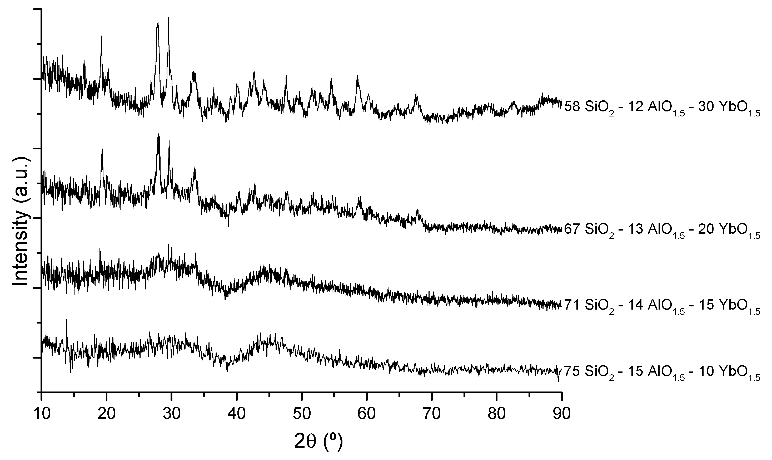
Figure 2.
X-ray diffraction patterns of silicon and two aluminosilicate films with 15 and 20 mol% YbO1.5, heat treated at 1100 °C.
Figure 2.
X-ray diffraction patterns of silicon and two aluminosilicate films with 15 and 20 mol% YbO1.5, heat treated at 1100 °C.

Figure 3.
Raman spectra of Yb-doped aluminosilicate bulk glasses. The samples were heat treated at 1050 °C, except for the sample labelled (*) which was heat-treated at 1100 °C.
Figure 3.
Raman spectra of Yb-doped aluminosilicate bulk glasses. The samples were heat treated at 1050 °C, except for the sample labelled (*) which was heat-treated at 1100 °C.
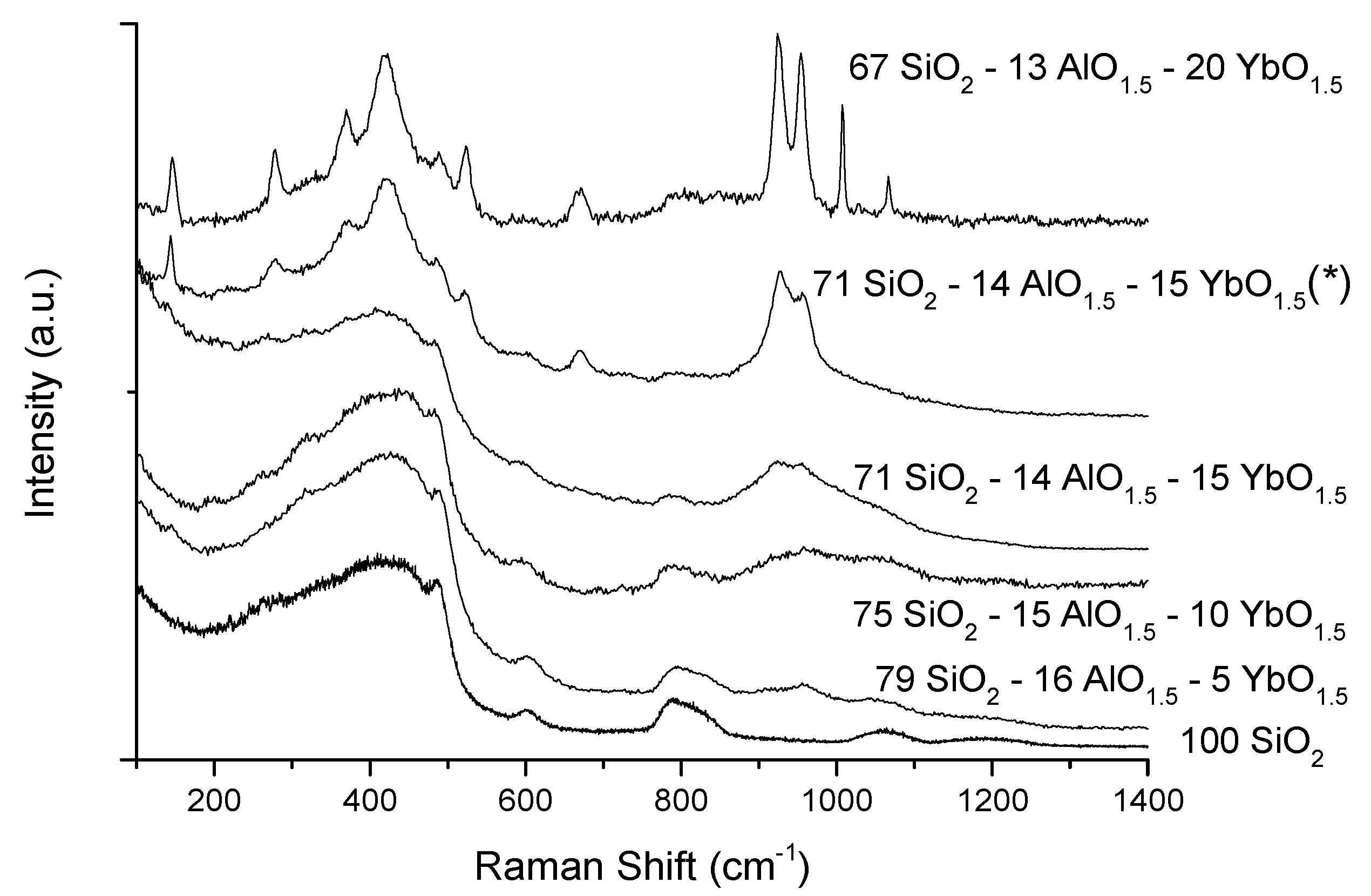
Figure 4.
Near infrared absorption spectrum of 79 SiO2-16 AlO1.5-5 YbO1.5 bulk gel.

Figure 5.
Normalized photoluminescence (PL) emission spectra of Yb/Er co-doped phosphosilicate bulk glass samples, excited at 970 nm.
Figure 5.
Normalized photoluminescence (PL) emission spectra of Yb/Er co-doped phosphosilicate bulk glass samples, excited at 970 nm.

Figure 6.
Normalized PL emission spectra of Yb/Er co-doped aluminosilicate bulk glass samples, excited at 970 nm.
Figure 6.
Normalized PL emission spectra of Yb/Er co-doped aluminosilicate bulk glass samples, excited at 970 nm.

Figure 7.
PL decay curves of aluminosilicate bulk glass samples doped with 5–30 mol% YbO1.5.
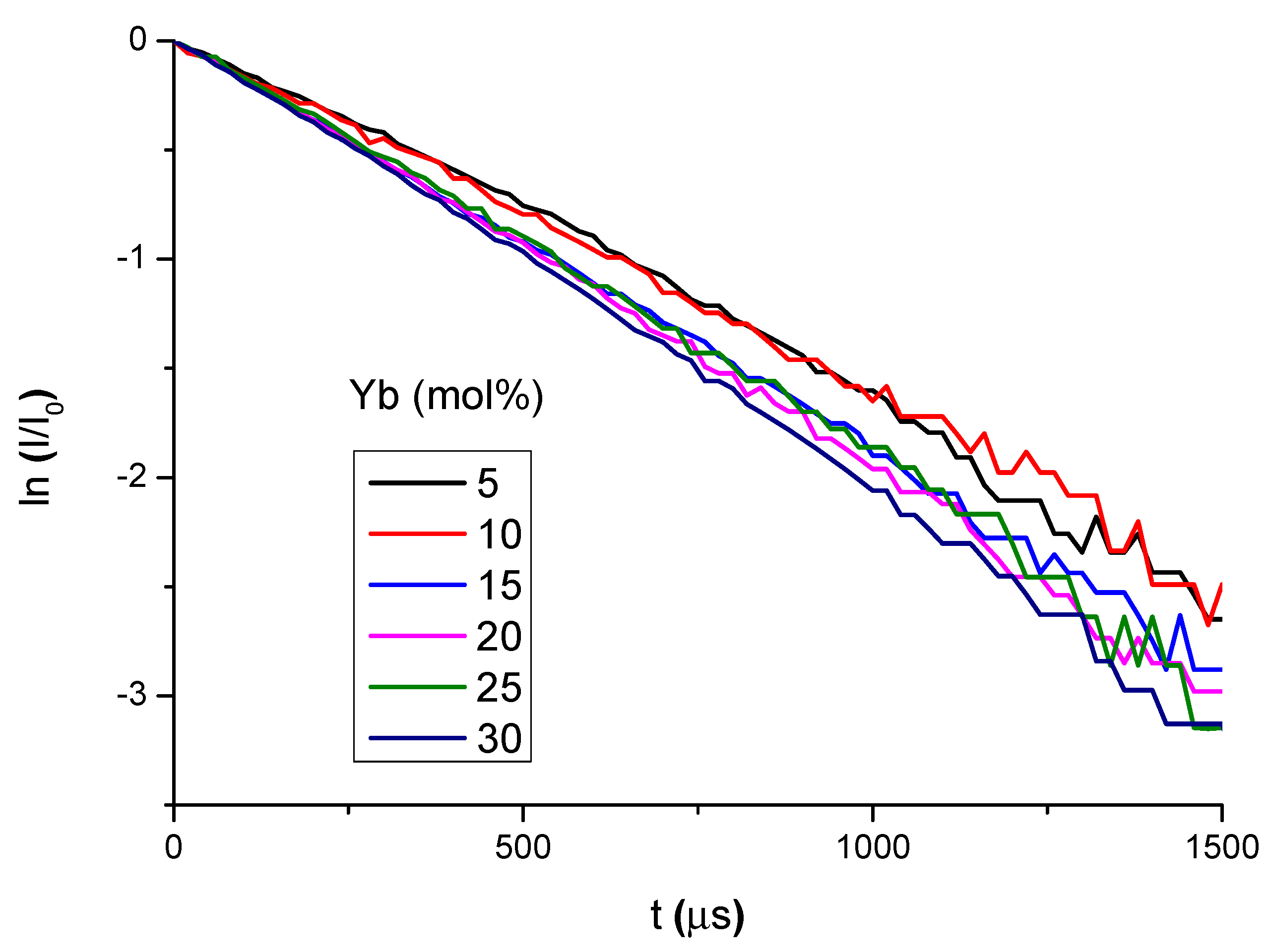
Figure 8.
Measured reflectance spectrum of a Bragg Mirror (BM) with 7 pairs of AS/T layers deposited on a Si wafer, compared with Transfer Matrix Method (TMM) simulation.
Figure 8.
Measured reflectance spectrum of a Bragg Mirror (BM) with 7 pairs of AS/T layers deposited on a Si wafer, compared with Transfer Matrix Method (TMM) simulation.
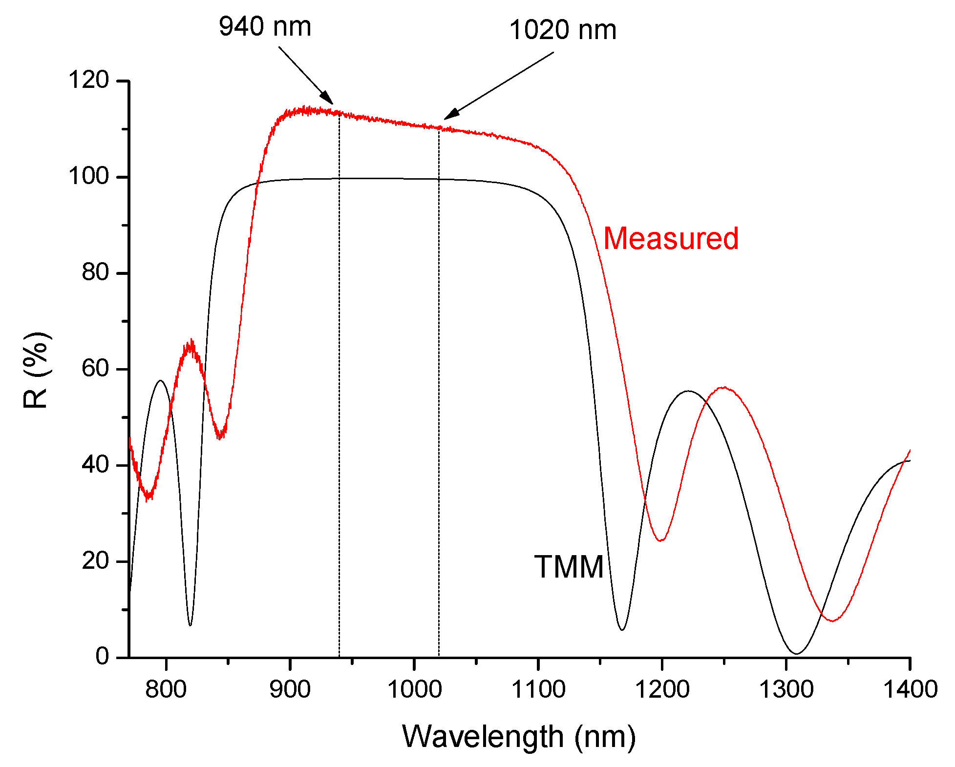
Figure 9.
Transmission of an anti-reflective coating (ARC) with 3 layers deposited on 71 SiO2-14 AlO1.5-15 YbO1.5 glass film deposited on silicon substrate, compared with TMM simulation.
Figure 9.
Transmission of an anti-reflective coating (ARC) with 3 layers deposited on 71 SiO2-14 AlO1.5-15 YbO1.5 glass film deposited on silicon substrate, compared with TMM simulation.
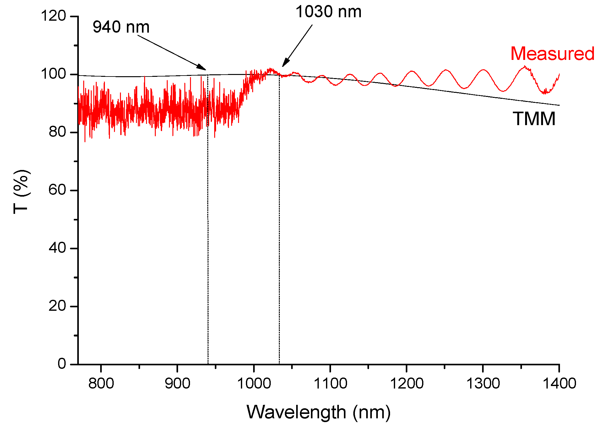
Figure 10.
FEG-SEM cross section micrograph of a ~10 μm thick active disk doped with 15 mol% YbO1.5, obtained in secondary electron mode. (Scale bar = 1 μm).
Figure 10.
FEG-SEM cross section micrograph of a ~10 μm thick active disk doped with 15 mol% YbO1.5, obtained in secondary electron mode. (Scale bar = 1 μm).
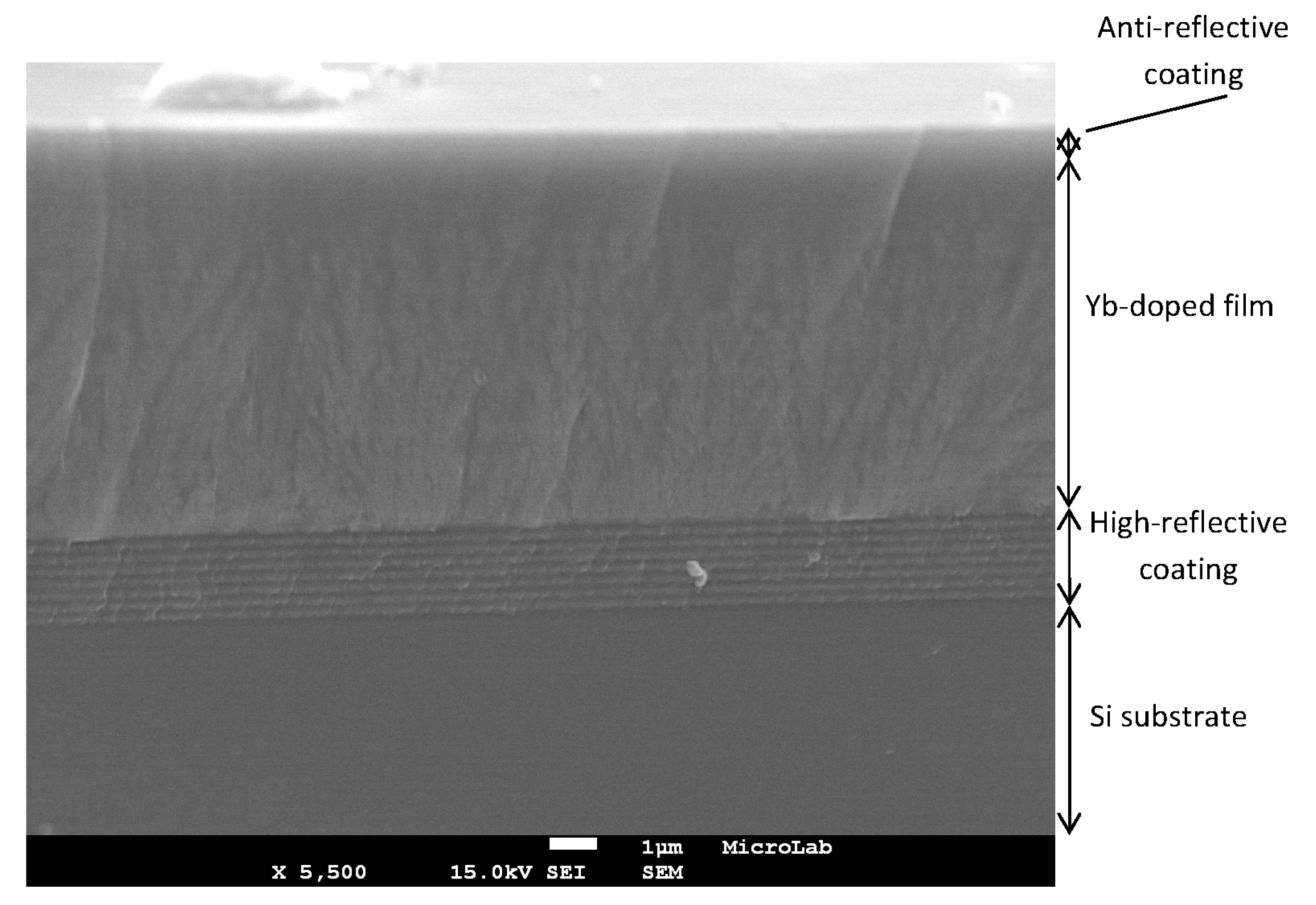
Figure 11.
X-ray diffraction patterns of an active disk (BM/36.3 μm thick 71 SiO2-14 AlO1.5-15 YbO1.5 film/ARC) on a silicon substrate.
Figure 11.
X-ray diffraction patterns of an active disk (BM/36.3 μm thick 71 SiO2-14 AlO1.5-15 YbO1.5 film/ARC) on a silicon substrate.
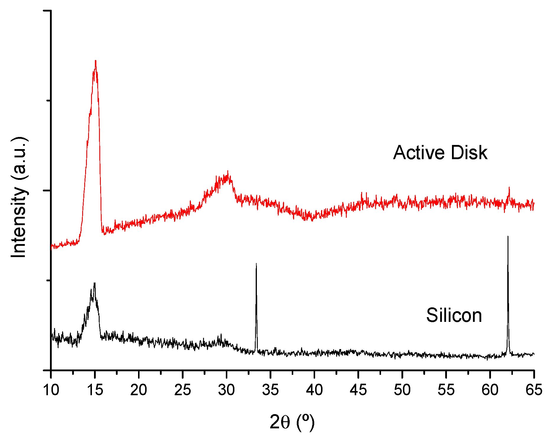
Figure 12.
Reflectance of an active disk composed of a BM, an Yb-doped layer (36.3 micron thick) and an ARC coating, deposited on silicon.
Figure 12.
Reflectance of an active disk composed of a BM, an Yb-doped layer (36.3 micron thick) and an ARC coating, deposited on silicon.
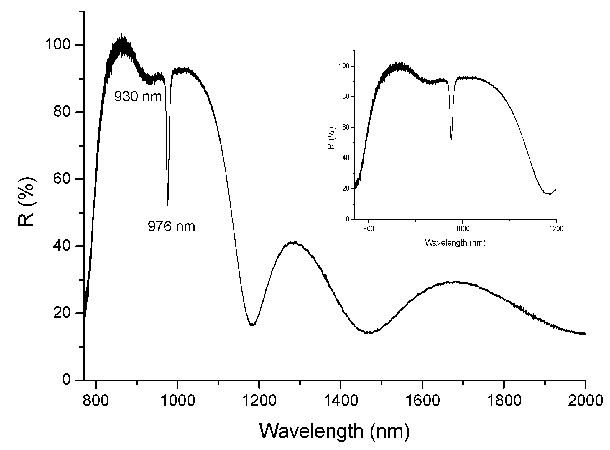
Figure 13.
PL emission spectrum of an active disk (BM/71 SiO2-14 AlO1.5-15 YbO1.5 film, 36.3 μm thick/ARC), excited at 970 nm.
Figure 13.
PL emission spectrum of an active disk (BM/71 SiO2-14 AlO1.5-15 YbO1.5 film, 36.3 μm thick/ARC), excited at 970 nm.
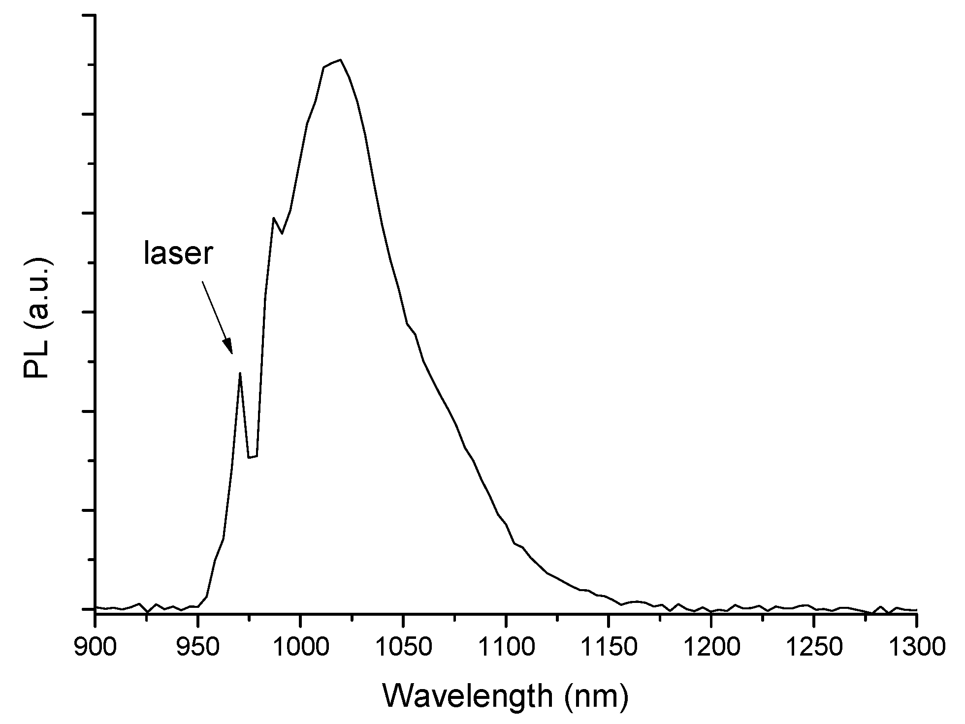
Figure 14.
Schematic structure of the active disks prepared.

Table 1.
Lifetime, τ and σ × τ values for Yb-doped phosphosilicate glasses.
| YbO1.5 (mol%) | τ (μs) | σ × τ (μs) |
|---|---|---|
| 3 | 1043 | 1126 |
| 5 | 782 | 1718 |
| 7 | 763 | 1528 |
| 10 | 735 | 5931 |
| 13 | 828 | 5845 |
| 15 | 586 | 4173 |
| 20 | 485 | 4039 |
| 30 | 542 | 4652 |
Table 2.
Lifetime, τ and σ × τ values for Yb-doped aluminosilicate glasses.
| YbO1.5 (mol%) | τ (μs) | σ × τ (μs) |
|---|---|---|
| 5 | 624 | 5509 |
| 10 | 614 | 8586 |
| 15 | 525 | 9648 |
| 20 | 511 | 11699 |
| 25 | 528 | 6349 |
| 30 | 482 | 7762 |
Table 3.
Rare-earth doped phosphosilicate and aluminosilicate glass compositions (mol%).
| SiO2 | PO2.5 | AlO1.5 | YbO1.5 |
|---|---|---|---|
| 81 | 16 | − | 3 |
| 79 | 16 | − | 5 |
| 77 | 16 | − | 7 |
| 75 | 15 | − | 10 |
| 73 | 14 | − | 13 |
| 71 | 14 | − | 15 |
| 67 | 13 | − | 20 |
| 58 | 12 | − | 30 |
| 79 | − | 16 | 5 |
| 75 | − | 15 | 10 |
| 71 | − | 14 | 15 |
| 67 | − | 13 | 20 |
| 63 | − | 12 | 25 |
| 58 | − | 12 | 30 |
© 2017 by the authors. Licensee MDPI, Basel, Switzerland. This article is an open access article distributed under the terms and conditions of the Creative Commons Attribution (CC BY) license (http://creativecommons.org/licenses/by/4.0/).
Share and Cite
MDPI and ACS Style
Almeida, R.M.; Ribeiro, T.; Santos, L.F. Sol-Gel Derived Active Material for Yb Thin-Disk Lasers. Materials 2017, 10, 1020. https://doi.org/10.3390/ma10091020
AMA Style
Almeida RM, Ribeiro T, Santos LF. Sol-Gel Derived Active Material for Yb Thin-Disk Lasers. Materials. 2017; 10(9):1020. https://doi.org/10.3390/ma10091020
Chicago/Turabian StyleAlmeida, Rui M., Tiago Ribeiro, and Luís F. Santos. 2017. "Sol-Gel Derived Active Material for Yb Thin-Disk Lasers" Materials 10, no. 9: 1020. https://doi.org/10.3390/ma10091020
Note that from the first issue of 2016, this journal uses article numbers instead of page numbers. See further details here.