Optimal Structure of a Plasmonic Chip for Sensitive Bio-Detection with the Grating-Coupled Surface Plasmon-Field Enhanced Fluorescence (GC-SPF)


1
School of Science and Technology, Kwansei Gakuin University, 2-1 Gakuen, Sanda, Hyogo 669-1337, Japan
2
Inorganic Functional Materials Research Institute, National Institute of Advanced Industrial Science and Technology (AIST), 1-8-31 Midorigaoka, Ikeda, Osaka 563-8577, Japan
*
Author to whom correspondence should be addressed.
Materials 2017, 10(9), 1063; https://doi.org/10.3390/ma10091063
Submission received: 11 July 2017
/
Revised: 14 August 2017
/
Accepted: 5 September 2017
/
Published: 11 September 2017
(This article belongs to the Special Issue Advance in Plasmonics and Metamaterials)
Abstract
:Surface plasmon field-enhanced fluorescence (SPF) has been one of the powerful tools for biosensors and bioimaging. A wavelength-scale periodic structure coated with a thin metal film is called a plasmonic chip, and it can provide SPF. SPF of Cy5-streptavidin (Cy5-SA) was measured on a biotinylated plasmonic chip with a grating of 480 nm-pitch. The optimal structure of a plasmonic sensor-chip was designed for improving detection sensitivity. The silver film thickness dependence of the SPF intensity was measured under the irradiation of the top panel of a sensor chip. Furthermore, the dependence of the SPF intensity on the distance from the metal surface was also investigated. The optimal structure for the largest fluorescence enhancement factor was 150 nm-thick silver and 10 nm-thick SiO2 layers due to the enhanced electric field (excitation field), the surface plasmon coupled emission (SPCE), and the interference effect with reflected light. The largest enhancement factor was found to be 170-fold. Furthermore, not only the largest fluorescence intensity but also stable lower background noise were found to be essential for higher-sensitive detection.
1. Introduction
Surface plasmon field-enhanced fluorescence (SPF) has been known as one of the powerful tools in immunosensors [1,2]. This is because fluorescence is a sensitive technique compared with methods measuring absorbance and reflectivity, and further, enhanced fluorescence can improve the detection sensitivity compared with the general fluorescence method. In SPF, the surface plasmon resonance (SPR) field is utilized as an excited field for fluorescent molecules. SPR is classified to propagating SPR and localized SPR. Localized SPR has been shown in nanoparticle-arrays and nanostructure-arrays with a size of several nm to several tens of nm [3,4]. Recently, localized SPR has been mainly studied for surface-enhanced Raman scattering (SERS) spectroscopy [3,5], photochemical reaction [6,7], light harvesting [8], and photonics [9,10]. It has the advantage of strongly enhanced electric field, but the area of the enhanced field is quite limited. On the other hand, localized SPR and propagating SPR have also been applied to SPF [11,12,13]. In fluorescence immunosensors, a large area is generally required for a sensor chip. So, propagating-SPF has an advantage due to the fabrication of a regular nano-structure array in a wide region and the less strict control of a distance from a metal surface compared with a localized-SPF. Basically, the fluorescence enhancement can be interpreted from the improvement of fluorescence quantum efficiency in Jablonski diagrams [14]. The fluorescence quantum efficiency η is given by η = kr/(kr + knr) using radiative and nonradiative decay rate constants, respectively. When the molecule is located on the plasmonic chip, energy transfer to surface plasmons with a rate ksp’ and interband or intraband transitions with a rate kisw’ were added, and fluorescence quantum efficiency was modified to η’= kr’/(kr’ + knr + ksp’ + kisw’). Moreover, when the possibility for the plasmon to reradiate is added as the probability χ = Гr/(Гr + Гa), where Гr and Гa are the radiative decay rate and the absorption decay rate, respectively, η’ is given by
η’ = (kr’ + χksp’)/(kr’ + knr + ksp’ + kisw’)
The enhancement factor for quantum efficiency is
η’/η = (kr’ + χksp’) (kr + knr)/kr (kr’ + knr + ksp’ + kisw’)
The fluorescence enhancement based on the excitation process is found to be composed of the increase of quantum efficiency and the enhanced excited-field.
In propagating SPR, there are prism-coupled SPR (PC-SPR) and grating-coupled SPR (GC-SPR). Early biosensors were based on PC-SPF [11], but GC-SPF has recently been applied to biosensors [15,16,17,18]. Wavelength-scale periodic structure coated with metal films is essential for GC-SPF method. We call it a plasmonic chip [15,16,17,18,19,20], which has been used as a sensor-chip. The plasmonic chip used with the SPF method has an overlayer composed of dielectric medium such as SiO2 on the metal film. The roles of the SiO2 layer are the protection of the metal layer from oxidation, suppression of a fluorescence quench by a metal layer [21], and the formation of an appropriate environment for biomaterial. The excited light can be incident from the top or bottom of a chip. The resonance condition is described as
where kspp, kph, and kg are the wavenumber vectors of the surface plasmon, the incident light, and the grating proportional to the inverse of pitch, respectively [22,23]. kspp was composed of complex dielectric constants for the metal and dielectric medium at the interface. m is an integer and θ is an incident angle or a detection angle (i.e., surface plasmon resonance angle for excitation and peak angle for surface plasmon coupled emission (SPCE), respectively) [24,25].
kspp = kph·sin θ ± m·kg,
Immunosensors using GC-SPF have been applied to detect various biomarkers [15,16,17,26]. In the detection of α-fetoprotein, the plasmonic chip can quantitatively detect until 2 pg/mL, in which the illumination was incident from the top side of the chip. The detection limit was quite low, but it can be further improved if the fluorescence enhancement factor can increase by optimizing the structure of a plasmonic chip (i.e., silver-film thickness and SiO2-film thickness), maintaining the pitch size and groove depth. In this study, the interaction between Cy5 fluorescently-labeled streptavidin and biotin modified with the surface of a plasmonic chip was used to study the improvement of fluorescence enhancement on the plasmonic chip as the model system. The light source was a He-Ne laser with the wavelength of 632.8 nm, and emission with a wavelength of 670 nm was detected for Cy5 (Figure S1). The SPCE peak can be detected at the direction normal to surface, 0 degree, which is the resonance condition as denoted by Equation (3) at wavelength of 670 nm. The SPCE peaks obtained at ±θ can overlap at 0 degrees, and the single peak has a higher intensity than double peaks separated at ±θ degrees. The optimal plasmonic chip structure including duty ratio, groove depth, and shape was already studied in our previous papers [18,19]. In this study, the plasmonic structure of pitch and groove depth was kept, and the silver film thickness and the silica film thickness were studied in order to improve the fluorescence enhancement factor in the top illumination system.
2. Results
2.1. Surface Analysis
Plasmonic chips with various silver film thickness or various SiO2 film thickness were fabricated, and they were measured by atomic force microscopy (AFM) (Figure S2). Cross-section contour of AFM images provided the slope α for a wall of convex in a periodic structure (Figure 1a,b), and surface roughness Ra was evaluated as the mean value of each Ra measured along the top of each convex line and the bottom of each groove line in AFM images (see Figure S2). Figure 1c shows the results of Ra and slope α plotted against the silver-film thickness. As the silver-film thickness increased, the roughness also gradually increased, and the slope was loose until silver film thickness of 200 nm, and then the slope kept constant over 200 nm.
2.2. SPF Measurement
2.2.1. Silver-Film Thickness Dependence of the Fluorescence Intensity
Silver-film thickness dependence of fluorescence intensity was investigated for the two types of optical systems; the detection angles scanning under the incident angle were fixed to 45 degrees, corresponding to out-of-resonance angle (DAS) and the incident angles scanning under the detector were fixed to 60 degrees, corresponding to out-of-SPCE angle (IAS). From IAS, the fluorescence intensities excited at resonance angle (peak) and out-of-resonance angle (base) were evaluated. Similar to IAS, the fluorescence intensities detected at SPCE angle (peak) and out-of-SPCE angle (base) were evaluated in DAS.
Figure 2c shows the fluorescence intensities for peaks and baselines in both DAS and IAS plotted against the silver-film thickness. The fluorescence intensities at base increased similarly to those at resonance peaks as the silver film became thick. Therefore, Figure 2 shows the silver-film thickness dependence of fluorescence enhancement by not only the plasmonic effect, but also the other optical effect. The surface roughness Ra—obtained by AFM images—also increased with the silver film thickness (as shown in Figure 1c), and the increase of fluorescence intensities was considered to be due to the increase of scattering effect based on the surface roughness.
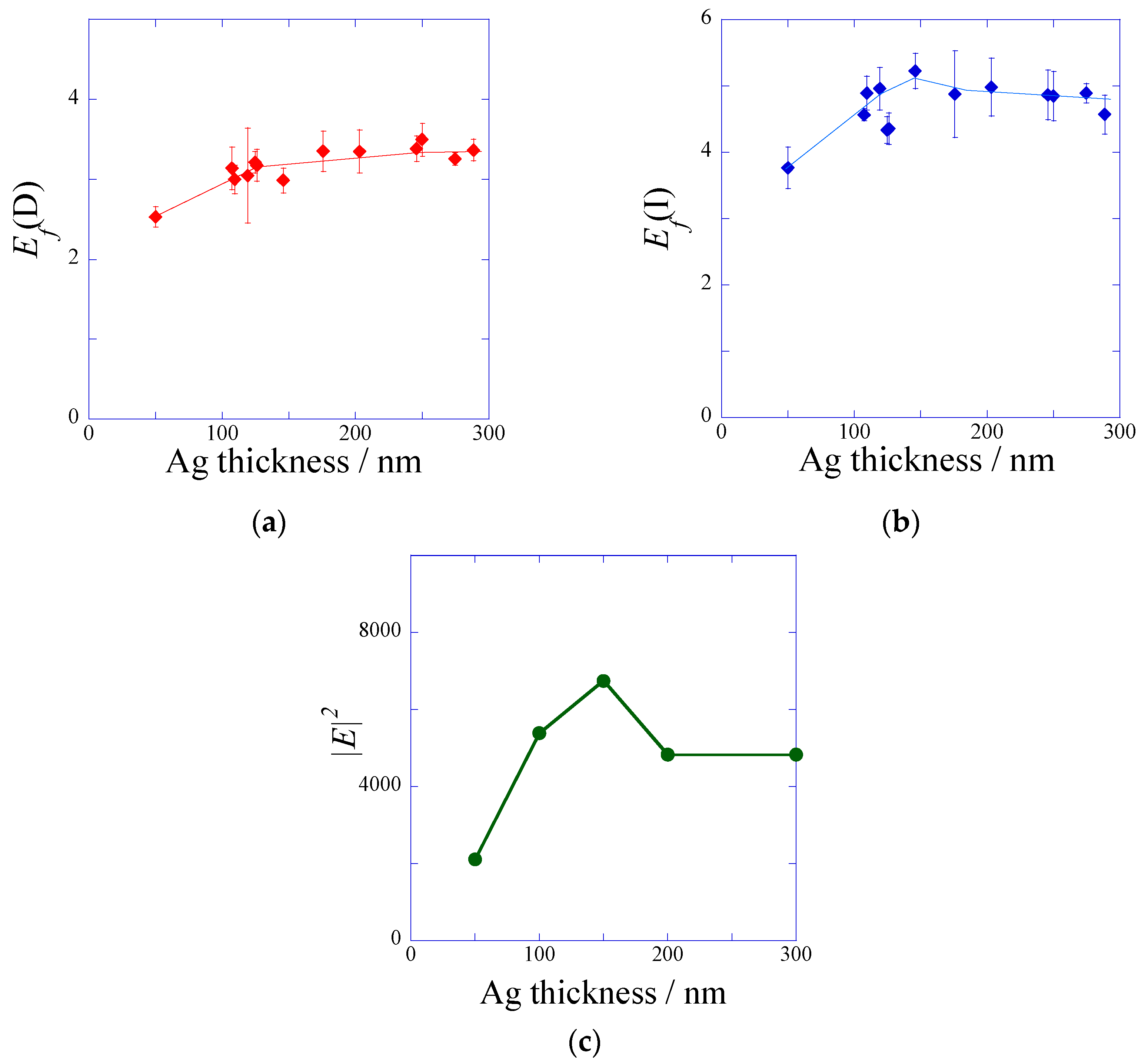
Plasmonic enhancement factors Ef(D) and Ef(I) were evaluated from the ratio of fluorescence intensity at peak to that at base in DAS and IAS systems in order to remove the scattering effect. As shown in Figure 3a, Ef(D) for SPCE effect increased up to around 150 nm-thick silver film, and it kept constant above 150 nm. In the Ef(I) for excited field enhancement shown in Figure 3b, the effect increased up to 150 nm and then it decreased over 150 nm. In both DAS and IAS, the increases of Ef(D) and Ef(I) for thinner silver film between 50 and 150 nm was considered to be due to suppressing the transmittance of illumination light by a silver film and improving the coupling efficiency between plasmon and light. On the other hand, the decrease of Ef(I) for thicker silver film (more than 150 nm) was explained by the Finite-difference time-domain method (FDTD) simulation result (Figure 3c). The slope of wall for a convex in a periodic structure was loose at silver film thickness over 200 nm as shown in Figure 1c. In FDTD simulation, when the parameter of slope keeps constant, the electric field also keeps for silver film thickness of more than 150 nm. However, when the value of incline analyzed from AFM cross-section contour was applied to the calculation parameter in FDTD, the electric field steeply decreased at 150 nm-thick silver film. This is consistent with the decrease of Ef(I).
The fluorescence intensity increased with silver-film thickness by the scattering effect due to the surface roughness. On the other hand, the coupling efficiency between incident light and surface plasmon, which is composed of suppressing the transmittance of incident light and the effect of incline of convex in periodic structure, were also considered to contribute to the fluorescence enhancement. Therefore, the surface selective fluorescence originating from GC-SPR was found to be maximized in 150 nm-thick silver film. The largest Ef(D) and Ef(I) values were found to be 3.2 and 5.1, respectively. The total plasmon effect of Ef(D) × Ef(I) was considered to be 16-fold. On the other hand, the fluorescence intensity was measured for the same assay on the glass slide as a reference. The mean fluorescence intensity on the glass slide was 1.8 × 10⁶ and 1.5 × 10⁶ in DAS and IAS, respectively. When the fluorescence intensities at base measured in DAS and IAS for 150 nm-thick silver film were divided by the mean fluorescence intensity on the glass slide, their values corresponded to the fluorescence enhancement factor by the reflection interference effect Ef(R), and they were between 2.5-fold and 3-fold. Therefore, if the fluorescence excited at SPR angle was detected at SPCE peak, around 50-fold (Ef(D) × Ef(I) × Ef(R) = 3.2 × 5.1 × 3) was obtained as the fluorescence enhancement Ef.
2.2.2. Dependence of the Fluorescence Intensity on the Distance from the Metal Surface
The SiO2 overlayer of a plasmonic chip was prepared in various film thicknesses between 8–300 nm. The SiO2 film thickness was controlled by the sputtering time and the film thickness was evaluated with theoretical fitting of the reflectivity spectra measured by PC-SPR. The linearity between the sputtering time and SiO2 film thickness was confirmed previously. SiO2-film thickness corresponds to the distance from a metal surface, and the SiO2 layer suppresses fluorescence quench. The fluorescence curves were measured by DAS and IAS, and both fluorescence intensities for DAS and IAS evaluated under the resonance (peak) and off resonance (base) were plotted against the distance from a metal surface as shown in Figure 4a,b, respectively. In IAS and DAS, the most enhanced fluorescence was observed at the distance of 30–40 nm. The distance was larger than the values predicted from fluorescence quench to the silver film [27]. The enhanced fluorescence intensity includes three kinds of distance dependence; i.e., an exponential decay of an enhanced electric field by SPR, an excited energy transfer (=quench) to the metal surface by Förster energy transfer [28], and an electric field enhanced by the interference effect between incident light and reflection light. Except for the decay of an electric field, the quench effect and the interference effect were observed even for the flat metal surface or under off resonance. The distance dependences of the fluorescence intensities observed in the base (off resonance) in IAS and DAS were almost equivalent, and they were consistent with the square of the electric field intensity due to the reflection interference calculated by FDTD (Figure S3).
In a similar way to the metal film thickness dependence, the peak values were divided by the base values in DAS and IAS, individually, in order to remove the fluorescence quench and reflection interference effect by a metal film. The SiO2-film thickness dependences of Ef(D) and Ef(I) are shown in Figure 5a,b, respectively. In both cases, the largest fluorescence enhancement factor was observed at a distance of around 10 nm, and Ef decreased to 1 at several hundreds of nm. Their behaviors were based on the decay of the plasmon field. The fluorescence quench was known to disappear at 10 nm, which is the Förster radius between a thin silver film and a dye molecule discussed in the Chance-Prock-Silbey (CPS) model [27,28]. At SiO2 film thickness less than 10 nm, the fluorescence quench effect strongly depends on the distance from the metal surface, and it is very difficult to completely remove the quenching effect under 10 nm. The largest enhancement factors in DAS and IAS were found to be 6.5-fold and 8.7-fold at 10 nm from a silver surface (Figure 5a,b).
2.3. Limit of Detection for IAS and DAS
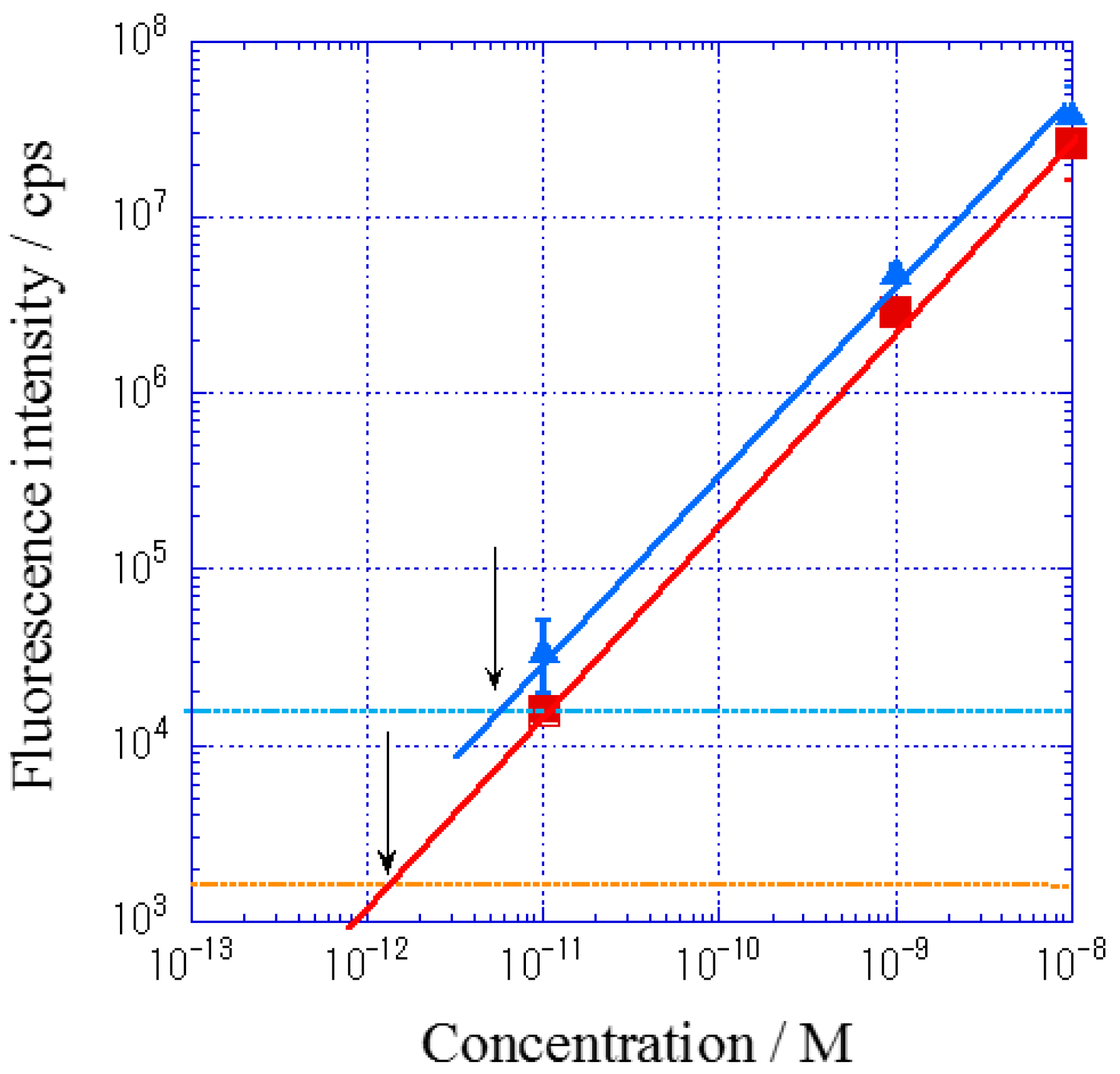
Figure 6 shows the calibration curve for Cy5-streptavidin (Cy5-SA). Fluorescence intensities were measured at three kinds of Cy5-SA concentration in DAS and IAS systems, and their mean values at peaks are plotted in Figure 6. The calibration curve in IAS is shown in the upper line in Figure 6, and each value was larger than that in DAS, depicted in the lower line. The standard deviation (SD) values in IAS were also larger than those in DAS, possibly due to the larger light scattering. The cross points of calibration curve and +SD line of background (as shown with arrows in Figure 6) indicate the limit of detection. Though the larger fluorescence intensity was observed in IAS, more sensitive detection was obtained in DAS.
3. Discussion
The fluorescence enhancement factor Ef evaluated from the multiplication of Ef(I) and Ef(D) was plotted against the distance from a metal surface (Figure 7). The most enhanced fluorescence could be detected at the SPCE peak angle under the illumination at the incident angle of SPR. In this study, the resonance angle was 8 degrees for the plasmonic chip prepared with the silver-film thickness of 150 nm and the SiO2-film thickness of 10 nm. So, a detection angle of 0 degree means that the detector was set to 8 degrees against the incident beam line. In the configuration of the optical system, the detector was not set to 8 degrees, because the incident beam was blocked (Figure 8). The enhancement factor due to Ef(I) and Ef(D) reached 57-fold from calculation, as shown in Figure 7. When the plasmonic chip was used for immuno-detection, the fluorescence intensity measured included the three-fold reflection interference effect compared with the fluorescence intensity on the glass slide, and total enhancement reached around 170-fold (=57 × 3). The fluorescence enhancement factors have been reported in the other system. S. Bae et al. reported the values of 10–14 for silver nanowire based on the localized SPR [29], and Y. Wang et al. reported 100 times for fluorescence co-enhanced by localized SPR and propagating SPR [30]. Among the SPF systems, the enhancement factor of 170-fold based on the GC-SPR was the larger value. Higher sensitivity detection can be achieved by suppressing the background noise. As shown in Figure 6, comparing the limit of detection between IAS and DAS, IAS showed a larger fluorescence intensity than that in DAS and had larger standard deviation in background. As a result, the sensitive detection was observed in DAS, suppressing the standard deviation of background. Highly sensitive detection of biomarkers can be achieved by the largest fluorescence enhancement and the smallest deviation of background.
4. Materials and Methods
4.1. Fabrication of a Plasmonic Chip
The periodic structure of the plasmonic chip was fabricated by UV-nanoimprint method. The details were shown in a previous study [31]. The replica was coated with thin films of titanium silver, titanium, and silica in order. Titanium films were prepared with film thickness less than 1 nm. The other film thicknesses are summarized in Table 1. The pitch, groove depth, and duty ratio of the plasmonic chip were 480 nm, 27 nm, and 0.5, respectively.
Although the SPR angle was independent of the silver-film thickness, it shifted to higher angle as SiO2-film thickness increased (Figure S4).
4.2. Surface Measurement
The plasmonic chip was measured by AFM (SPI3800N, SII, Chiba, Japan). The mean surface roughness Ra was evaluated from roughness on the lines of convex part. The pitch and groove depth were also evaluated from AFM images. From cross-section contour, the slope of a wall for convex was evaluated.
4.3. Samples
All the plasmonic chips were modified with 3-aminopropyltriethoxysilane (APTES; Sigma-Aldrich, St. Louis, MO, USA) by silane-coupling reaction and biotin-polyethylene glycol-succinimide (NHS-PEGBio; BI-050TS, NOF, Tokyo, Japan) by chemical reaction with the amino group of APTES. Cover glass was attached to the sensor-chip with double-sided tape, and a gap was satisfied with solution by capillary phenomena. Cy5-SA (GE Healthcare, Little Chalfont, UK) prepared at 10 nM was applied to the fluorescence intensity measurement in order to optimize the plasmonic structure. For fluorescence measurement, the distance from the metal surface over 300 nm was prepared using 370 nmφ- or 4500 nmφ-microbeads as a binder and the cover glass modified with NHS-PEGBio was attached to the plasmonic chip. The Cy5-SA can be bound to biotin in the cover glass side. Furthermore, in order to make a comparison of the detection sensitivity between IAS and DAS systems, Cy5-SA was prepared at the concentrations of 10, 1 nM, and 10 pM, and their florescence intensity was measured by SPF setup.
4.4. Fluorescence Measurement
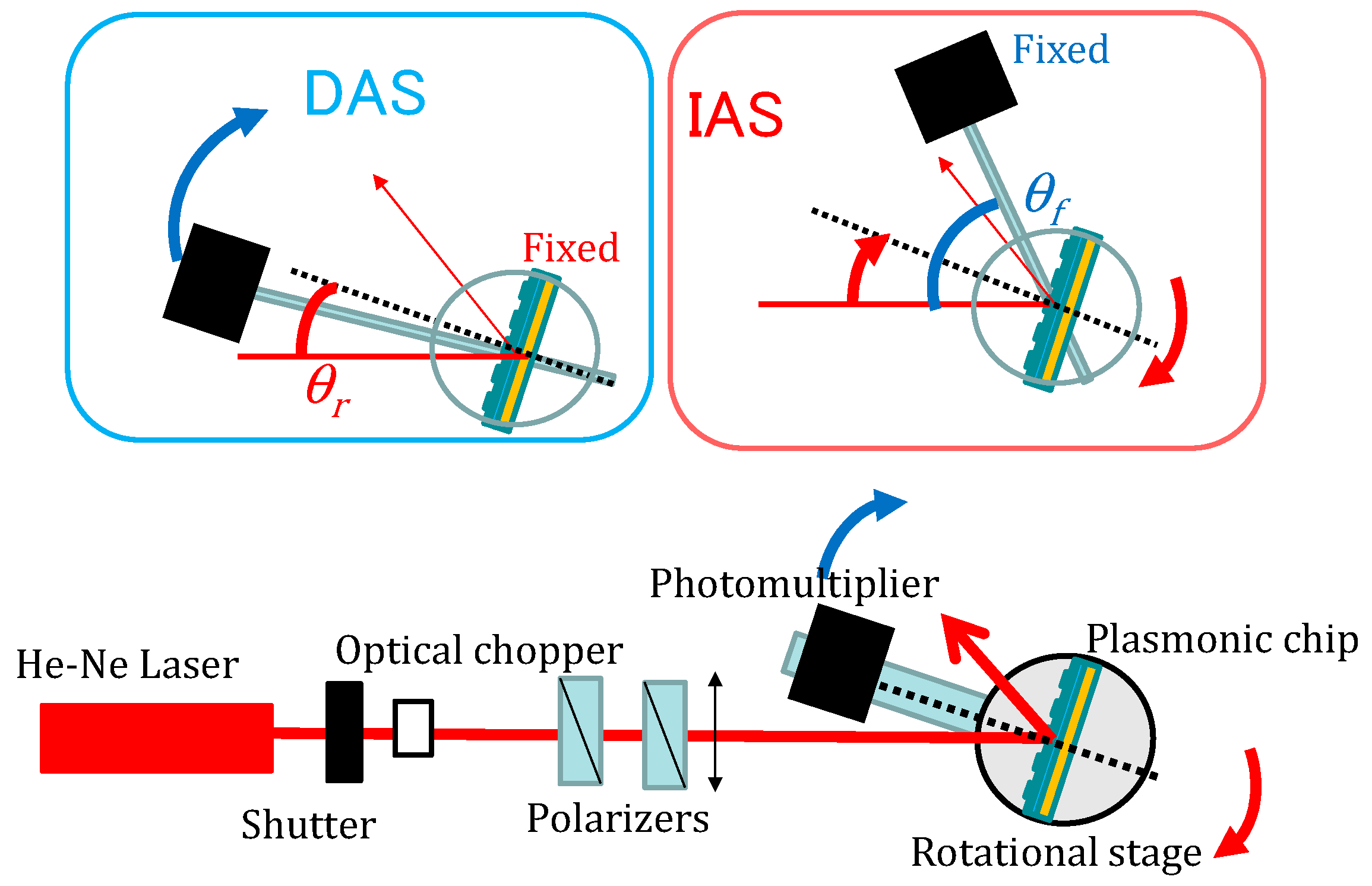
The measurement method is briefly shown here, and details were described in the previous papers [15,17,18]. A He-Ne laser beam of 632.8 nm wavelength with 1 mW passes through an optical chopper and two polarizers for intensity and polarization control. Using a θ-2θ goniometer, the light reflected on the substrate was monitored against an incident angle (θi) of 5–30 degrees by a Si photodiode. The diameter of the illumination spot was about 1 mm. The emission was monitored by a photomultiplier tube (after passing through lenses and a narrow band interference filter (λ = 670 + 5 nm) and a notch filter (Stopline, NF03-633E, Semrock, New York, NY, USA) mounted on the goniometer unit instead of a Si photodiode. Incident angle θi and detection angle θf were defined as the angle between the laser beam line and normal to the chip and the angle between the direction of the detector and normal to the chip, respectively (Figure 8). For the incident light from the top of a panel, fluorescence intensity was measured against the detection angle between 10 and 15 or 50 degrees at the fixed incident angle of 45 degrees (DAS; left panel of upper in Figure 8) and that against the incident angle between 5 and 30 or 60 degrees at the fixed detection angle of 60 degrees (IAS; right panel of Figure 8, upper).
4.5. Numerical Analysis
The electric field near the surface of the grating patterns was calculated using the two-dimensional FDTD (FullWAVE, RSOFT, Synopsys Mountain View, CA, USA) method [32]. The calculation parameters for the grating models were as follows: the silica grating patterns had a pitch of 480 nm and a groove depth of 30 nm. The thickness of the silver layer was varied between 0–300 nm, and a 20 nm-thick SiO2 overlayer was prepared for the study of the silver film thickness-dependence of the fluorescence enhancement. Furthermore, the thickness of the SiO2 layer was varied between 10–300 nm, and a 150 nm-thick-silver layer was prepared for the study of the SiO2 film thickness-dependence of the fluorescence enhancement. A trapezoidal model was used as a surface profile. From the cross-sectional areas measured by AFM, the incline (slope) of a wall for convex was evaluated. The computational parameters of slope of a wall for convex were determined from cross-section contours for plasmonic chips fabricated as shown in Figure 1c. Calculations were executed for two periodically repeating units drawn using non-uniform grids ranging from 5 nm to 1 μm to reduce the computational time. The smallest grids of 5 nm were used for the regions close to the interface. A periodic boundary condition was used for the unit-cell edges in the direction orientated normal to the grating surface, and a perfectly matched layer absorbing boundary condition was used for the edges in the direction orientated parallel to the grating surface. The refractive index of SiO2 for an overlayer and a grating substrate, and of silver, was used as n = 1.457 and k = 0 and n = 0.015 and k = 4.13, respectively. The refractive index of water was used as n = 1.33. The FDTD computations were carried out in an incident plane with a wavelength of 632.8 nm and the polarization of transverse magnetic mode. The light source was placed in the matrix, and therefore, the incident angle of the propagating light into water was converted to the angle in air to adjust to the SPF experimental conditions.
5. Conclusions
A plasmonic chip can enhance the fluorescence intensity of fluorescent dye by the GC-SPF. The optimal structure of a sensor-chip was found to be covered with 150 nm-thick silver film and 10 nm-thick SiO2 film with a grating of 480 nm pitch under the irradiation from the top panel of a sensor chip. Enhancement factor is composed of Ef(I) by the enhanced electric field (excitation field), Ef(D) by the surface plasmon coupled emission (SPCE), and Ef(R) by the reflection interference effect. The largest plasmonic enhancement calculated by Ef(D) × Ef(I) was 57-fold. The total enhancement factor adding reflection interference effect Ef(R) was found to be around 170-fold. The enhanced fluorescence also induces a large deviation in background due to the scattering light. Therefore, not only the largest fluorescence intensity, but also the stable lower background noise were the most important factors for the sensitive detection.
Supplementary Materials
The following are available online at www.mdpi.com/1996-1944/10/9/1063/s1. Figure S1: Cy5 absorption and fluorescence spectra from web page of GE healthcare. Figure S2: AFM images of plasmonic chips with various silver-film thickness and a top view of AFM image. Each silver-film thickness is: (a) 0 (replica before coating), (b) 49, (c) 126, (d) 175, (e) 203, (f) 245, (g) 250, (h) 275, (i) 288 nm, respectively. The surface roughness Ra was evaluated as the mean value of each Ra measured along the top of each convex line and the bottom of each groove line in AFM images as depicted with lines in (j). Figure S3: The square of the electric field intensity on the flat metal-coated substrate calculated against the distance from metal surface by FDTD method. Figure S4: (a) Reflectivity measured against the incident angle (SPR curves) for the plasmonic chip with SiO2- film thickness of 8 (red cross, ×), 16 (orange full circle, ●), 30 (green square, □), 41 (green full triangle, ▲), 72 (blue triangle, ▽), 140 (blue full square, ■), 200 (purple circle, ○), 300 (gray diamond, ◇) nm. (b) The SPR angle plotted against the SiO2-film thickness
Acknowledgments
K.T. thanks Toyo Gosei for providing the UV-curable resin PAK-02-A. This work was supported by JSPS KAKENHI Grant Numbers 25286032 in Scientific Research (B).
Author Contributions
K.T. conceived and designed the experiments, and wrote the paper; K.K. designed the calculation; T.N. performed the experiments and calculation and analyzed the data.
Conflicts of Interest
The authors declare no conflict of interest.
References
- Vareiro, M.L.M.; Liu, J.; Knoll, W.; Zak, K.; Williams, D.; Jenkins, A.T.A. Surface plasmon fluorescence measurements of human chorionic gonadotrophin: Role of antibody orientation in obtaining enhanced sensitivity and limit of detection. Anal. Chem. 2005, 77, 2426–2431. [Google Scholar] [CrossRef] [PubMed]
- Chang, Y.F.; Chen, R.C.; Lee, Y.J.; Chao, S.C.; Su, L.C.; Li, Y.C.; Chou, C. Localized surface plasmon coupled fluorescence fiber-optic biosensor for alpha-fetoprotein detection in human serum. Biosens. Bioelectron. 2009, 24, 1610–1614. [Google Scholar] [CrossRef] [PubMed]
- Willets, K.A.; Van Duyne, R.P. Localized Surface Plasmon Resonance Spectroscopy and Sensing. Annu. Rev. Phys. Chem. 2007, 58, 267–297. [Google Scholar] [CrossRef] [PubMed]
- Hao, E.; Schatz, G.C. Electromagnetic fields around silver nanoparticles and dimers. J. Chem. Phys. 2004, 120, 357–366. [Google Scholar] [CrossRef] [PubMed]
- Lim, D.K.; Jeon, K.S.; Hwang, J.H.; Kim, H.; Kwon, S.; Suh, Y.D.; Nam, J.M. Highly uniform and reproducible surface-enhanced Raman scattering from DNA-tailorable nanoparticles with 1-nm interior gap. Nat. Nanotechnol. 2011, 6, 452–460. [Google Scholar] [CrossRef] [PubMed]
- Ueno, K.; Misawa, H. Surface plasmon-enhanced photochemical reactions. J. Photochem. Photobiol. C-Photochem. Rev. 2013, 15, 31–52. [Google Scholar] [CrossRef]
- Linic, S.; Christopher, P.; Ingram, D.B. Plasmonic-metal nanostructures for efficient conversion of solar to chemical energy. Nat. Mater. 2011, 10, 911–921. [Google Scholar] [CrossRef] [PubMed]
- Beck, F.J.; Polman, A.; Catchpole, K.R. Tunable light trapping for solar cells using localized surface plasmons. Appl. Phys. 2009, 105, 114310. [Google Scholar] [CrossRef]
- Tagliabue, G.; Höller, C.; Eghlidi, H.; Poulikakos, D. Proximal gap-plasmon nanoresonators in the limit of vanishing inter-cavity separation. Nanoscale 2014, 6, 10274–10280. [Google Scholar] [CrossRef] [PubMed]
- Zayats, A.V.; Smolyaninov, I.I. Near-field photonics: Surface plasmon polaritons and localized surface plasmons. J. Opt. A Pure Appl. Opt. 2003, 5, S16. [Google Scholar] [CrossRef]
- Liebermann, T.; Knoll, W. Surface-plasmon field-enhanced fluorescence spectroscopy. Colloids Surf. A 2000, 177, 115–130. [Google Scholar] [CrossRef]
- Tawa, K.; Knoll, W. Mismatching base-pair dependence of the kinetics of DNA-DNA hybridization studied by surface plasmon fluorescence spectroscopy. Nucleic Acids Res. 2004, 32, 2372–2377. [Google Scholar] [CrossRef] [PubMed]
- Zhang, J.; Fu, Y.; Chowdhury, M.H.; Lakowicz, J.R. Metal-enhanced single-molecule fluorescence on silver particle monomer and dimer: Coupling effect between metal particles. Nano Lett. 2007, 7, 2101–2107. [Google Scholar] [CrossRef] [PubMed]
- Hayashi, S.; Okamoto, T. Plasmonics: Visit the past to know the future. J. Phys. D Appl. Phys. 2012, 45, 433001. [Google Scholar] [CrossRef]
- Tawa, K.; Kondo, F.; Sasakawa, C.; Nagae, K.; Nakamura, Y.; Nozaki, A.; Kaya, T. Sensitive Detection of a Tumor Marker, α-Fetoprotein, with a Sandwich Assay on a Plasmonic Chip. Anal. Chem. 2015, 87, 3871–3876. [Google Scholar] [CrossRef]
- Matsuura, R.; Tawa, K.; Kitayama, Y.; Takeuchi, T. A Plasmonic Chip-Based Bio/Chemical Hybrid Sensing System for the Highly Sensitive Detection of C-Reactive Protein. Chem. Commun. 2016, 52, 3883–3886. [Google Scholar] [CrossRef] [PubMed]
- Tawa, K.; Umetsu, M.; Nakazawa, N.; Hattori, T.; Kumagai, I. Application of 300× Enhanced Fluorescence on a Plasmonic Chip Modified with a Bispecific Antibody to a Sensitive Immunosensor. ACS Appl. Mater. Interfaces 2013, 5, 8628–8632. [Google Scholar] [CrossRef] [PubMed]
- Tawa, K.; Hori, H.; Kintaka, K.; Kiyosue, K.; Tatsu, Y.; Nishii, J. Optical microscopic observation of fluorescence enhanced by grating-coupled surface plasmon resonance. Opt. Express 2008, 16, 9781–9790. [Google Scholar] [CrossRef] [PubMed]
- Cui, X.Q.; Tawa, K.; Hori, H.; Nishii, J. Tailored Plasmonic Gratings for Enhanced Fluorescence Detection and Microscopic Imaging. Adv. Funct. Mater. 2010, 20, 546–553. [Google Scholar] [CrossRef]
- Tawa, K.; Yasui, C.; Hosokawa, C.; Aota, H.; Nishii, J. In Situ Sensitive Fluorescence Imaging of Neurons Cultured on a Plasmonic Dish Using Fluorescence Microscopy. ACS Appl. Mater. Interfaces 2014, 6, 20010–20015. [Google Scholar] [CrossRef] [PubMed]
- D’Agostino, S.; Sala, F.D. Active Role of Oxide Layers on the Polarization of Plasmonic Nanostructures. ACS Nano 2010, 4, 4117–4125. [Google Scholar] [CrossRef] [PubMed]
- Räther, H. Surface Plasmons on Smooth and Rough Surfaces and on Gratings; Springer: Heidelberg, Germany, 1988; pp. 1–133. [Google Scholar]
- Knoll, W. Interfaces and Thin Films as Seen by Bound Electromagnetic Waves. Annu. Rev. Phys. Chem. 1998, 49, 569–638. [Google Scholar] [CrossRef] [PubMed]
- Malicka, J.; Gryczynski, I.; Gryczynski, Z.; Lakowicz, J.R. DNA Hybridization Using Surface Plasmon-Coupled Emission. Anal. Chem. 2003, 75, 6629–6633. [Google Scholar] [CrossRef] [PubMed]
- Wintera, G.; Barnes, W.L. Emission of light through thin silver films via near-field coupling to surface plasmon polaritons. Appl. Phys. Lett. 2006, 88, 051109. [Google Scholar] [CrossRef] [Green Version]
- Tsuneyasu, M.; Sasakawa, C.; Naruishi, N.; Tanaka, Y.; Yoshida, Y.; Tawa, K. Sensitive detection of interleukin-6 (IL-6) on a plasmonic chip by grating-coupled surface-plasmon-field-enhanced fluorescence imaging. Jpn. J. Appl. Phys. 2014, 53, 06JL05. [Google Scholar] [CrossRef]
- Chance, R.R.; Prock, A.; Silbey, R. Molecular Fluorescence and Energy Transfer Near Interfaces. Adv. Chem. Phys. 1978, 37, 1–65. [Google Scholar] [CrossRef]
- Tawa, K.; Morigaki, K. Substrate-Supported Phospholipid Membranes Studied by Surface Plasmon Resonance and Surface Plasmon Fluorescence Spectroscopy. Biophys. J. 2005, 89, 2750–2758. [Google Scholar] [CrossRef] [PubMed]
- Bae, S.; Jin, H.H.; Bae, G.; Lee, E.Y.; Im, S.H.; Kim, D.H.; Seo, T.S. Growth of Silver Nanowires from Controlled Silver Chloride Seeds and Their Application for Fluorescence Enhancement Based on Localized Surface Plasmon Resonance. Small 2017, 13, 1603392. [Google Scholar] [CrossRef] [PubMed]
- Wang, Y.; Wu, L.; Wong, T.I.; Bauch, M.; Zhang, Q.; Zhang, J.; Liu, Z.; Zhou, X.; Bai, P.; Dostalek, J.; et al. Directional fluorescence emission co-enhanced by localized and propagating surface plasmons for biosensing. Nanoscale 2016, 8, 8008. [Google Scholar] [CrossRef] [PubMed]
- Akashi, N.; Tawa, K.; Tatsu, Y.; Kintaka, K.; Nishii, J. Grating Substrates Fabricated by Nanoimprint Lithography for Fluorescence Microscopy. Jpn. J. Appl. Phys. 2009, 48, 06FH17. [Google Scholar] [CrossRef]
- Hori, H.; Tawa, K.; Kintaka, K.; Nishii, J.; Tatsu, Y. Surface Profile Dependence on the Grating-Coupled Surface Plasmon Enhanced Fluorescence. J. Appl. Phys. 2010, 107, 114702. [Google Scholar] [CrossRef]
Figure 1.
(a) Atomic force microscopy (AFM) image; (b) Cross-section contour of AFM image shows slope, α; and (c) Ra and slope α plotted against the silver film thickness.
Figure 1.
(a) Atomic force microscopy (AFM) image; (b) Cross-section contour of AFM image shows slope, α; and (c) Ra and slope α plotted against the silver film thickness.
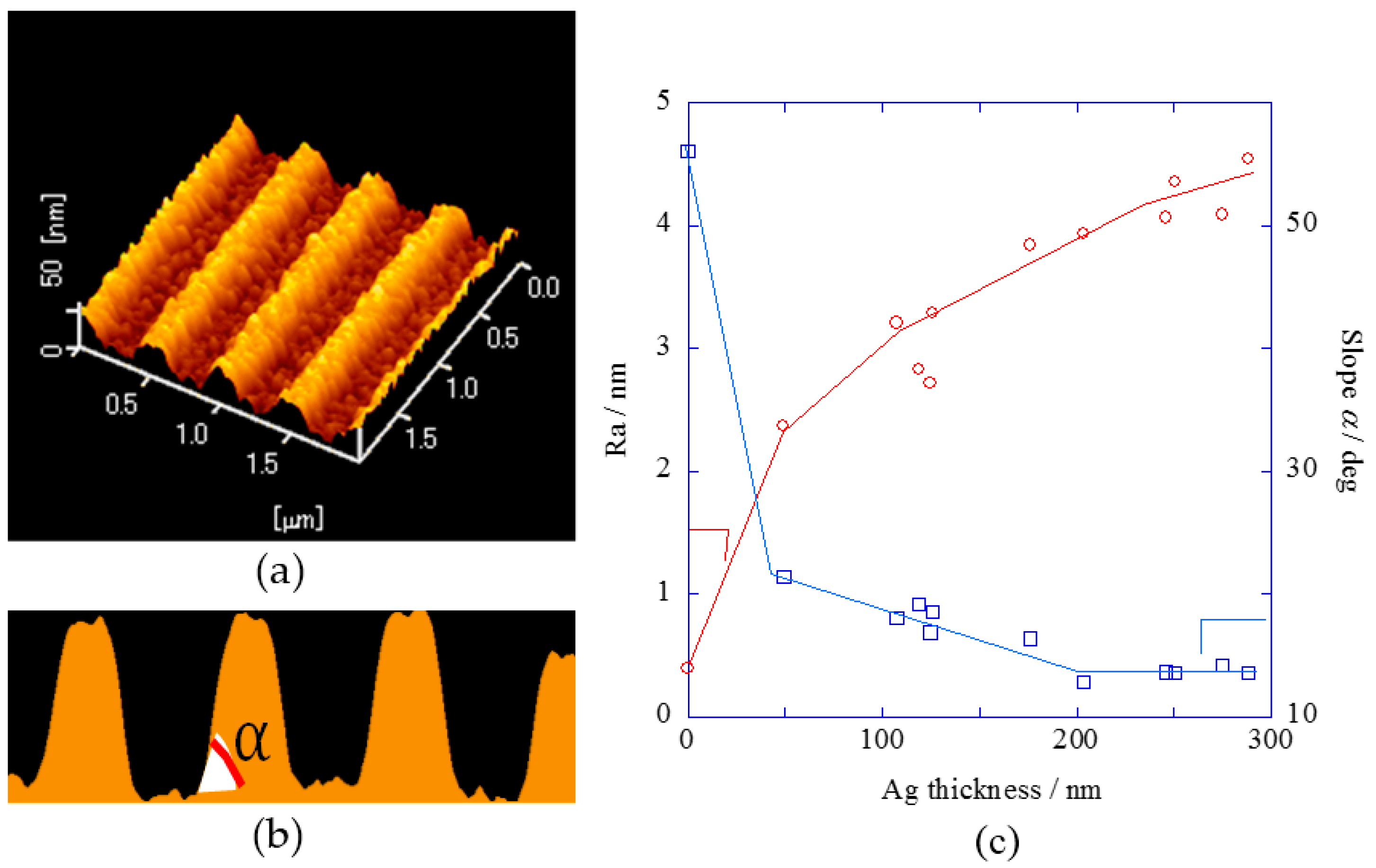
Figure 2.
Fluorescence intensities measured (a) against the detection angle under the excitation at out-of-resonance angle (DAS) system and (b) against the incident angle under the detection at out-of-SPCE (surface plasmon coupled emission) angle (IAS) system; and (c) fluorescence intensities plotted against the silver film thickness for the peak values in DAS (red solid line) and IAS (blue solid line) and for the base values in DAS (red broken line) and IAS (blue broken line).
Figure 3.
Enhancement factors against the silver film thickness in (a) DAS and (b) IAS measurement, which were evaluated as the fluorescence intensity at peak divided by the fluorescence intensity at baseline; and (c) the square of electric field intensity calculated against the silver film thickness by Finite-difference time-domain method (FDTD) method.

Figure 4.
Fluorescence peak (solid line and rhombuses) and base (broken line and triangles) intensities plotted against the distance from a metal surface (a) in DAS system and (b) in IAS system.
Figure 4.
Fluorescence peak (solid line and rhombuses) and base (broken line and triangles) intensities plotted against the distance from a metal surface (a) in DAS system and (b) in IAS system.

Figure 5.
Enhancement factor obtained from the peak values divided by the base values (a) in DAS system and (b) in IAS system.
Figure 5.
Enhancement factor obtained from the peak values divided by the base values (a) in DAS system and (b) in IAS system.
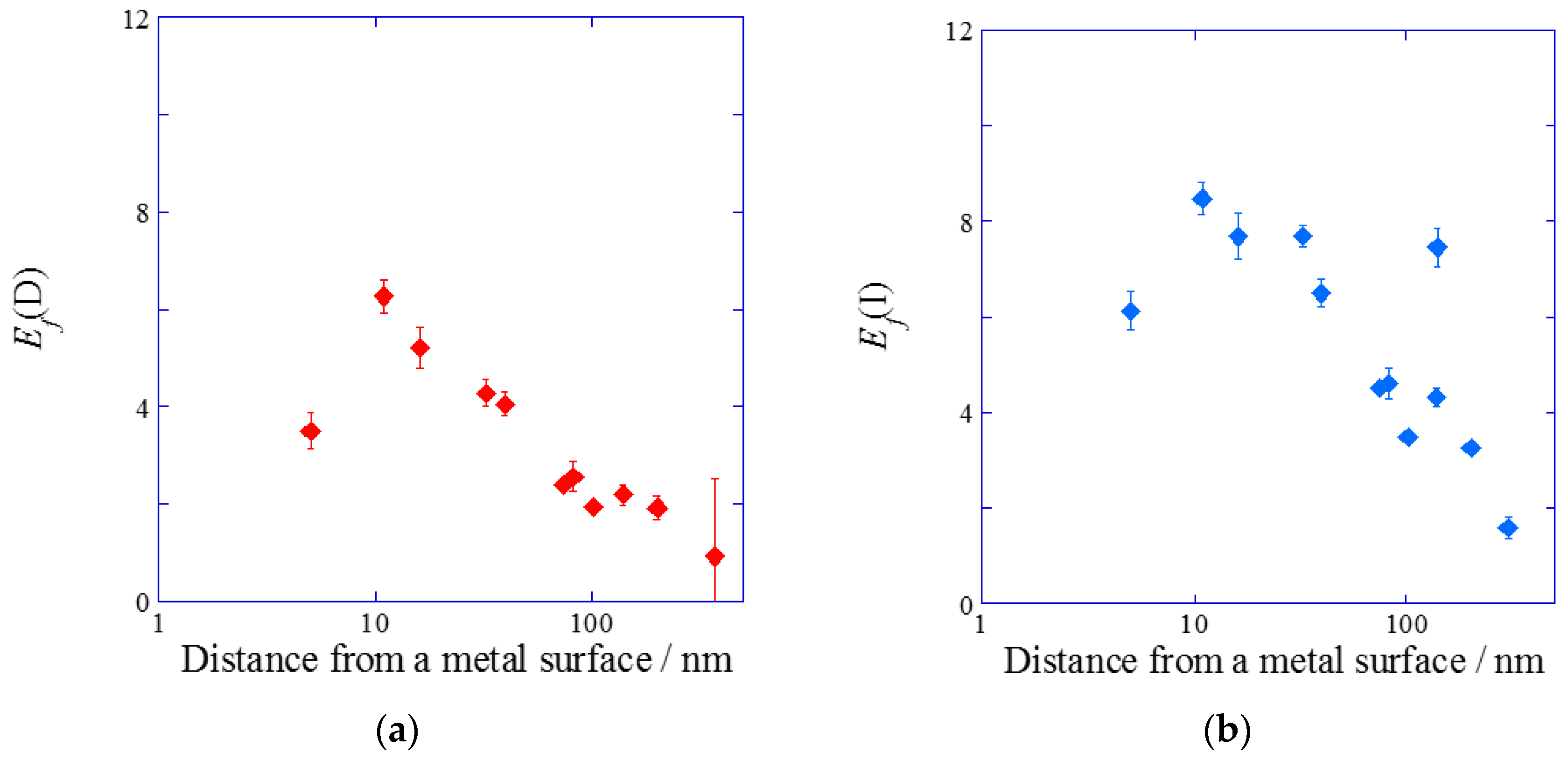
Figure 6.
Calibration curve for Cy5-streptavidin (Cy5-SA): blue line shows the plots for IAS system and red line shows those for DAS system. Two broken lines with blue and red correspond to the standard deviation of background for IAS and DAS, respectively.
Figure 6.
Calibration curve for Cy5-streptavidin (Cy5-SA): blue line shows the plots for IAS system and red line shows those for DAS system. Two broken lines with blue and red correspond to the standard deviation of background for IAS and DAS, respectively.

Figure 7.
Fluorescence enhancement factor multiplied the normalized peak value to base value for DAS and that for IAS.
Figure 7.
Fluorescence enhancement factor multiplied the normalized peak value to base value for DAS and that for IAS.
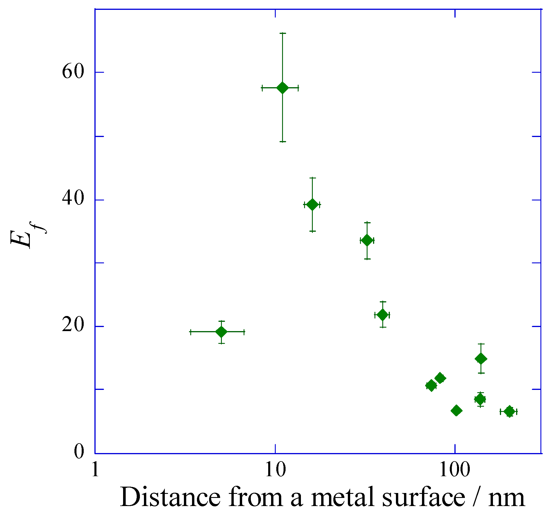
Figure 8.
Surface plasmon field-enhanced fluorescence (SPF) setup and optical configuration for DAS and IAS measurement system.
Figure 8.
Surface plasmon field-enhanced fluorescence (SPF) setup and optical configuration for DAS and IAS measurement system.


Table 1.
Each film thickness prepared for each experiment.
| Experiment | Silver/nm | SiO2/nm |
|---|---|---|
| Ag film thickness dependence | 50–288 | 20 ± 4 (fixed) |
| SiO2 film thickness dependence | 211 ± 8 (fixed) | 8–300 |
© 2017 by the authors. Licensee MDPI, Basel, Switzerland. This article is an open access article distributed under the terms and conditions of the Creative Commons Attribution (CC BY) license (http://creativecommons.org/licenses/by/4.0/).
Share and Cite
MDPI and ACS Style
Tawa, K.; Nakayama, T.; Kintaka, K. Optimal Structure of a Plasmonic Chip for Sensitive Bio-Detection with the Grating-Coupled Surface Plasmon-Field Enhanced Fluorescence (GC-SPF). Materials 2017, 10, 1063. https://doi.org/10.3390/ma10091063
AMA Style
Tawa K, Nakayama T, Kintaka K. Optimal Structure of a Plasmonic Chip for Sensitive Bio-Detection with the Grating-Coupled Surface Plasmon-Field Enhanced Fluorescence (GC-SPF). Materials. 2017; 10(9):1063. https://doi.org/10.3390/ma10091063
Chicago/Turabian StyleTawa, Keiko, Takuya Nakayama, and Kenji Kintaka. 2017. "Optimal Structure of a Plasmonic Chip for Sensitive Bio-Detection with the Grating-Coupled Surface Plasmon-Field Enhanced Fluorescence (GC-SPF)" Materials 10, no. 9: 1063. https://doi.org/10.3390/ma10091063
Note that from the first issue of 2016, this journal uses article numbers instead of page numbers. See further details here.