High-Quality GaSe Single Crystal Grown by the Bridgman Method
by
 , and
, and
Tao Wang
1,2,* ,
,
Jie Li
1,2,
Qinghua Zhao
1,2,
Ziang Yin
1,2,
Yinghan Zhang
1,2,
Bingqi Chen
1,2,
Yong Xie
3 and
Wanqi Jie
1,2 1
State Key Laboratory of Solidification Processing, Northwestern Polytechnical University, Xi’an 710072, China
2
Key Laboratory of Radiation Detection Materials and Devices, Ministry of Industry and Information Technology, Northwestern Polytechnical University, Xi’an 710072, China
3
State Key Discipline Laboratory of Wide Band Gap Semiconductor Technology, School of Advanced Materials and Nanotechnology, Xidian University, Xi’an 710071, China
*
Author to whom correspondence should be addressed.
Materials 2018, 11(2), 186; https://doi.org/10.3390/ma11020186
Submission received: 7 January 2018
/
Revised: 18 January 2018
/
Accepted: 22 January 2018
/
Published: 24 January 2018
(This article belongs to the Section Thin Films and Interfaces)
Abstract
:A high-quality GaSe single crystal was grown by the Bridgman method. The X-ray rocking curve for the studied GaSe sample is symmetric and the Full Width at Half Maximum (FWHM) is only 46 arcs, which is the smallest value ever reported for GaSe crystals. The IR-transmittance is about 66% in the range from 500 to 4000 cm−1. The photoluminescence spectrum at 9.2 K shows a symmetric and sharp excition peak in 2.1046 eV. The results indicate that the as-grown GaSe crystal is of high crystalline quality. The as-grown -GaSe crystal has a p-type conductance with the resistivity of 103 Ω/cm, and the Hall mobility is ~25 cm2 V−1 s−1. Few-layer GaSe crystals were prepared through mechanical exfoliation from this high-quality crystal sample. Few-layer GaSe-based photodetectors were fabricated, which exhibit an on/off ratio of 104, a field-effect differential mobility of 0.4 cm2 V−1 s−1, and have a fast response time less than 60 ms under light illumination.
1. Introduction
GaSe is known as a non-linear optical material, which possesses great potential in non-linear optical devices and THz generation [1,2,3,4,5,6,7,8]. Recently, two-dimensional (2D) GaSe materials have drawn the increasing attention of researchers because of their superior performance in optical and electrical aspects. Hu et al. [9] reported a photodetector based on few-layer GaSe materials for the first time, with an responsivity of 2.8 A/W under 254 nm illumination and a corresponding quantum efficiency of 1367%, which is much higher than MoS2 and other two-dimensional semiconductor materials, such as grapheme. Since then, many efforts have been made to improve the performance of 2D GaSe devices through changing the device structure or device processing [10,11,12]. Meanwhile, obtaining high-quality 2D GaSe materials is also an important way to improve device performance.
2D GaSe is often prepared by mechanical exfoliation from bulk GaSe [13,14,15] or grown by vapor phase transport techniques [16,17,18,19,20,21]. Lei et al. [16] reported vapor phase transport method to grow GaSe atomic layers for the first time, and the photoconductivity measurements shows an on/off ratio of 103. GaSe nanoplates epitaxial growth on transparent flexible mica substrates showed photo-responsivity of 0.6 A/W [17]. Recently, Xiong et al. [19] succeed in synthesizing GaSe nanoribbons through one step thermal deposition process. The GaSe nanoribbon-based photodetectors showed an on/off ratio of 103, a field-effect differential mobility of 0.03 cm2 V−1 s−1, and the response time is less than 0.3 s. In general, those methods use Ga/Ga2Se3 or Ga2Se3 as source materials, which may result in heterogeneous or non-stoichiometric composition and morphology. These introduced impurities and defects will finally deteriorate the performance of devices. Mechanical exfoliation is a promising method where the high quality can be inherited from the bulk crystal and large scale 2D GaSe can be obtained. However, most GaSe materials used to fabricate 2D GaSe devices through mechanical exfoliation were bought from commercial vendors, making it difficult to fully understand the properties of the materials. There have been many attempts to grow GaSe crystals [20,21,22,23,24,25,26,27], but the growth of high-quality bulk GaSe crystal is still a challenge. The great difference in saturation vapor pressure of the components Se and Ga can cause non-stoichiometry of a melt-grown crystal composition. Another obstacle is the dendrite growth caused by instability of the growth front [28]. The X-ray rocking curve and IR-transmittance results reveals that crystalline quality still needs to be improved. In addition, high-quality crystals are also required to reduce scattering and improve the phase matching for nonlinear applications.
In this work, we report our efforts on the grown of high-quality GaSe crystals by the Bridgman method. Great crystalline quality was exhibited by several methods. 2D GaSe devices were fabricated based on the high-quality crystal. The few-layered GaSe photodetector exhibits a high on/off ratio of 104, a field-effect differential mobility of 0.4 cm2 V−1 s−1, and has a response time less than 60 ms under light illumination.
2. Experimental Section
2.1. Synthesis of GaSe Polycrystals
High-purity Ga (6N, 99.9999%) and Se (6N, 99.9999%) from Emei Corp., Ltd. (Emei, China) was used as the raw material. The fused quartz ampoule coated with a carbon film was used to prevent adhesions. Gallium was baked at 673 K for 4 h under high vacuum to remove the oxide layer. Ga and Se were mixed in a stoichiometric ratio and sealed at 10−5 Torr. A single-temperature zone rocking furnace was used for synthesis.
2.2. Growth of Single-Crystal GaSe
A two-temperature zone furnace was used to grow the GaSe single crystal by the vertical Bridgman method. The upper and lower zones were set at 1293 K and 1173 K, separately, and the temperature gradient was 10 K/cm. The crystal growth rate was 0.5 mm/h. A BN-crucible with an inner diameter of 22 mm was used to grow the GaSe crystal.
2.3. Characterization Methods
The phase and crystal structure of the as-grown GaSe crystals were identified by powder X-ray diffraction. The rocking curve was obtained from (004) reflex of the cleaved GaSe face using an Empyrean X-ray diffraction machine (PANalytical, X’Pert Pro, Eindhoven, The Netherlands). The morphology was characterized by scanning electron microscopy (SEM) using a Supra-55 (Carl Zeiss, Jena, Germany). The composition of GaSe was measured by an electro-probe microanalyzer (EPMA; JXA-8100, JEOL, Tokyo, Japan). The infrared transmittance from 500 to 4000 cm−1 was measured by a Nicolet Nexus Fourier Transform Infrared Spectrometer (Nexus 670, Nicolet, Waltham, MA, USA). The optical energy gap at room temperature was determined by a UV-3150 ultraviolet visible/near-infrared spectrometer (Shimadzu, Kyoto, Japan). The photoluminescence spectrum was measured by using an argon ion laser with the wavelength of 488 nm and the luminescence signals were recorded with the spectrometer of TRIAX 550 (Jobin Yvon, Paris, France). The I–V characteristic curve was measured with an Agilent 4155C semiconductor parameter analyzer (Agilent, Santa Clara, CA, USA). The Hall measurement was carried out on Keithley HMS Model 7077 (Tektronix, Beaverton, OR, USA) to identify the carrier type and concentration, and to obtain the mobility of the sample in Van der Pauw geometry.
2.4. The Preparation of GaSe (Metal-Oxide Semiconductor Field-Effect Transistor) MOSFET Photodetector
Few-layered GaSe was obtained by mechanical exfoliation by using scotch tape. Photodetectors were fabricated on p-doped Si substrates with a 300 nm SiO2. A Ti (5 nm)/Au (50 nm) electrode was deposited on clean SiO2/Si substrates by magnetron sputtering assisted with a mask. Few-layered GaSe was transferred onto the electrodes using poly (dimethyl siloxane) (PDMS). The devices were annealed under high vacuum for 2 h at 200 °C to reduce contact resistance. Electrical measurements were made by using an Agilent 4155C (Agilent, Santa Clara, CA, USA) combined with a probe station.
3. Results and Discussion
3.1. Crystalline Structure and Composition
A GaSe ingot with diameter of 22 mm and length of 20 mm was obtained, as shown in Figure 1a. The crystal is transparent and shows rufous color with a light illumination. Figure 1b shows the sample cleaved along the (001) layers from as-grown ingots with no additional treatment or polishing of the surface. The whole surface indicates one large grain along the cleavage surface, and several voids are seen at the surface. Figure 1c shows a GaSe single-crystal wafer of 10 × 10 × 1 mm and Figure 1d indicates that it can be easily exfoliated because of the weak interlayer van der Waals interaction. The SEM pattern of the cleavage surface (see supplementary materials Figure S1) shows the laminated structure and it is atomically flat without any micro-cracks or defects.
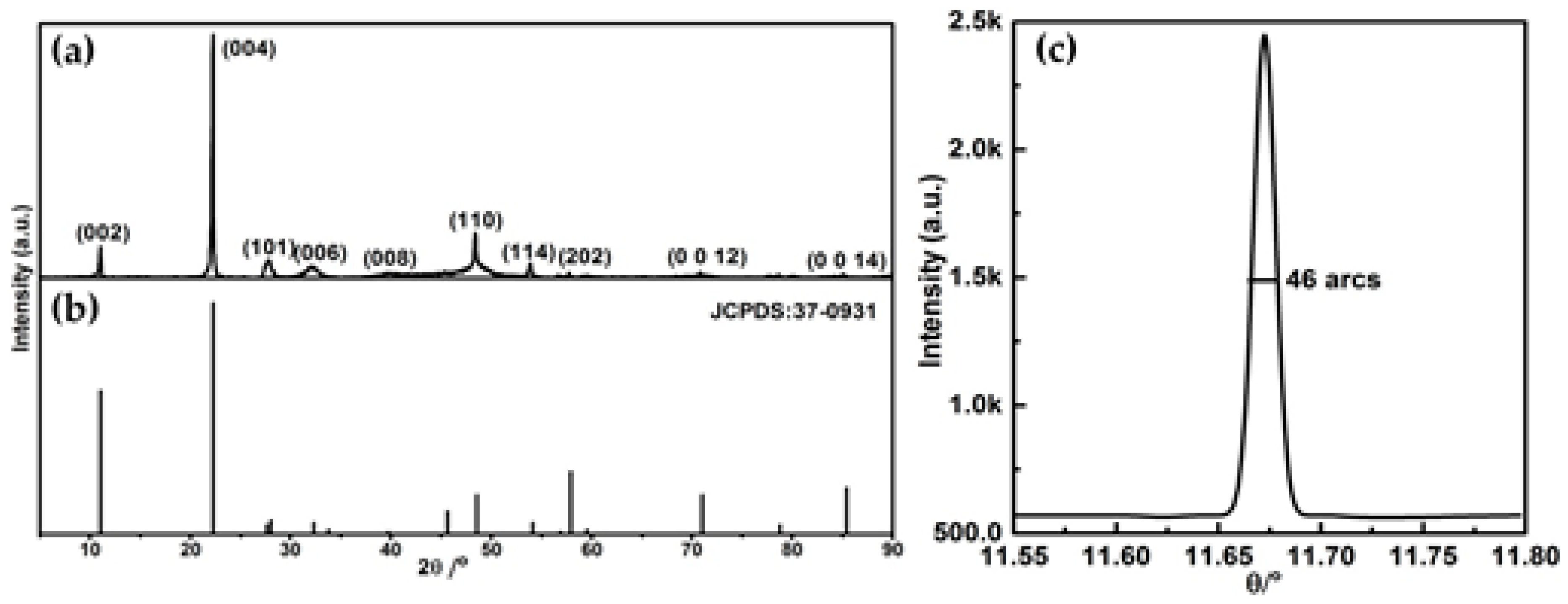
Figure 2a,b shows the powder diffraction pattern of the as-grown GaSe crystal and the theoretical curve of GaSe (JCPDS: 37-0931). They are in good agreement and confirm that hexagonal GaSe crystal is grown with cell parameters a = b = 3.749 Å, and c = 15.907 Å, space group D3h1 (Pm2).
Usually, the symmetry of the X-ray rocking curve is directly related to the structural uniformity of the crystal. Figure 2c shows the X-ray rocking curve of the (004) face of the as grown GaSe crystal. The peak shape is symmetric and the FWHM is about 46 arcs, which is the smallest values ever reported for GaSe crystals (0.15° in [20], split peaks in [21], 0.07° in [24], and 0.04° in [28]). The results indicated the as-grown GaSe crystals has a good crystalline quality.
Table 1 shows the composition distribution from the tip to tail of the GaSe ingot, as measured by EPMA. The Ga/Se ratio is near 1:1 and it is more close to stoichiometric ratio than some earlier reports [19,28]. The results of these measurements showed a good stoichiometry and homogeneity across the crystals. Slight Ga rich in composition is probably resulted from the loss of Se during synthesis and growth process because of its high vapor pressure.
3.2. Optical Measurements
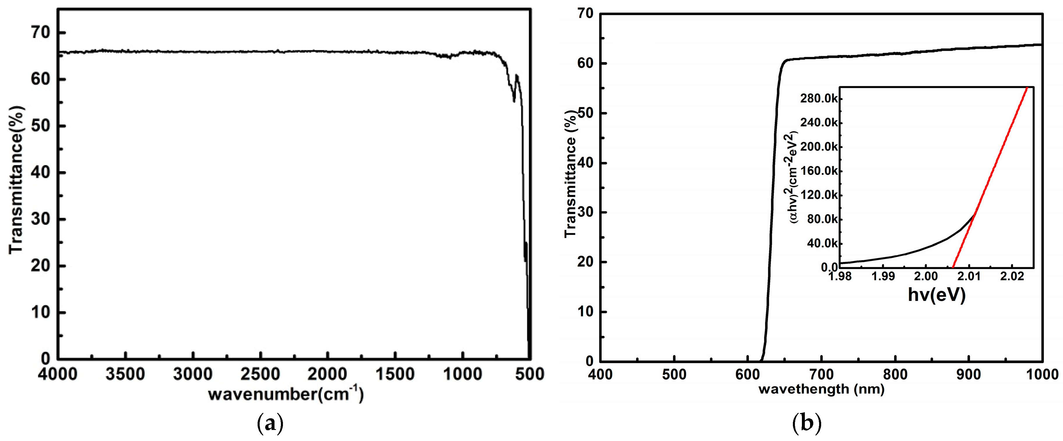
The infrared-transmission spectrum is shown in Figure 3a, and the infrared transmittance is about 66% over the all range from 500 to 4000 cm−1, which is the highest ever reported for GaSe crystals grown by the Bridgman method. The optical absorption coefficient was calculated by the equation in [29,30]. The absorption coefficient is as low as 0.18–0.2 cm−1 in the range of 0.9–14 μm (see Supplementary Materials, Figure S2), indicating the perfect optical quality of GaSe sample. The ultraviolet–visible–near-IR spectrum of GaSe over the wavelength range from 200 nm to 2600 nm is shown in Figure 3b, from which the band gap is determined to be about 2.00 eV at room temperature.
We also measured the photoluminescence (PL) spectrum of the as grown GaSe crystals at 9.2 K, which is shown in Figure 4. A dominant peak at 2.1046 eV was attributed to the direct free excitonic recombination. The strong and narrow peak with FWHM of 11 meV indicates excellent crystalline quality.
3.3. Electrical Measurements
Table 2 shows the Hall measurements of four GaSe samples taken from the tip to the tail of the ingot. All samples displayed p type conductivity and the hole concentration is about 1015 cm−3, with the mobility of ~20 cm2 V−1 s−1. The p-type conductivity may be contributed to the gallium vacancies (VGa), interstitial selenium atoms (SeI), and gallium atoms on selenium sites (GaSe) [31]. Since the composition measurement of the sample shows that Ga is slightly richer than Se, we conclude the p-type conductivity appeared, probably, due to the gallium atoms on selenium sites (GaSe). The hole mobility is lower than the theoretical value of 50 cm2 V−1 s−1 and this may be contributed by the defects or traps in the surface of GaSe wafer.
3.4. Characterization of the Few-Layered GaSe Photodetector
Figure 5a shows the schematic diagram of the few-layered GaSe photodetector on the SiO2/Si substrate, and Figure 5b is the optical image of the fabricated few-layered GaSe photodetector. Figure 5c,d shows the Atomic Force Microscopy (AFM) image and thickness of this GaSe photodetector. The thickness along the black line is about ~29 nm. Considering that single layer GaSe has a thickness of 0.93 nm, the thickness corresponds to ~31 layers of GaSe.
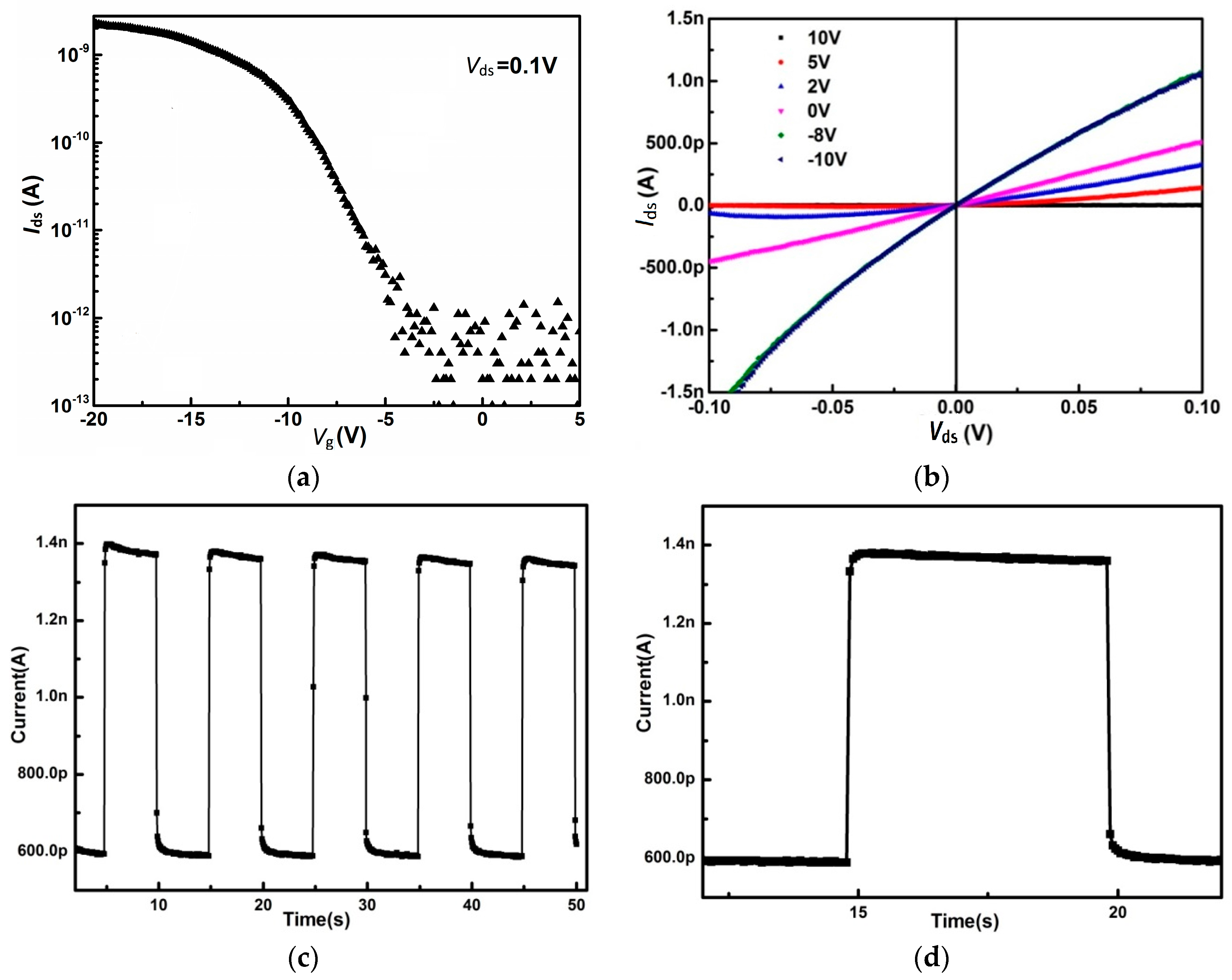
Figure 6a,b shows the room temperature Field-Effect Transistor (FET) transfer characteristics and output characteristics of this device. The few-layer GaSe FET device shows a typical p-type conductive behavior, which is “off” under a positive gate voltage and “on” under a negative gate voltage. The on/off ratio is about 104, which is comparable to earlier reports [13,14,19]. This high on/off ratio cannot be reached without the high-quality few-layered GaSe materials. The field-effect differential mobility of few-layered GaSe FET devices can be calculated by [10], where is the transconductance that equals to dIds/dVgs, which can be obtained from the transfer curve, L and W are the length (7.84 μm) and width (3.75 μm) of the channel, and Ci (6.9 × 10⁻⁵ F cm−2) is given by the equation Ci = ε0εr/d, where εr (3.9) and d (300 nm) are the dielectric constant and thickness of SiO2, respectively. The typical field-effect differential mobility for GaSe was calculated to be ≈0.4 cm2 V−1 s−1. Supposedly, the oxidation of the cleaved GaSe surface may be a source of this effect. At least, some comments could be given concerning this factor. The related information can be found elsewhere [32].
To further investigate the photoresponse of the device, a periodically-switched light with 520 nm was applied. The current exhibits a 1.5 nA light current and a 500 pA dark current, giving an Ilight/Idark ratio of ~3, which is shown in Figure 6c. Figure 6d is the time resolved photoresponse in a single period, the response time is less than 60 ms with a sharp rise and decay. The switching between “on” and “off” states is very fast and stable, allowing the device to act as a high-quality photosensitive switch. This demonstrates that few-layered GaSe may be a suitable candidate for future electronic and optical devices.
4. Conclusions
In summary, high-quality GaSe ingots 22 mm in diameter and about 20 mm in length were grown by the vertical Bridgman method. The X-ray rocking curve is symmetric and the FWHM is 46 arcs. The IR transmittance is about 66% over the wavenumber range from 500 to 4000 cm−1. The PL spectrum shows a sharp near-band peak with a FWHM of 11 meV. All these results revealed that the as-grown GaSe crystals possessed high crystalline quality. The few-layered GaSe-based photo-detectors exhibit a 104 on/off ratio, a field-effect differential mobility of 0.4 cm2 V−1 s−1, and have a fast response time less than 60 ms under light illumination.
Supplementary Materials
The following are available online at https://www.mdpi.com/1996-1944/11/2/186/s1, Figure S1. SEM pictures of GaSe (001) face; Figure S2. Calculated absorption coefficient of GaSe crystals.
Acknowledgments
This work was supported by the National Natural Science Foundations of China (No. 51672216) and the National Key R and D Program of China (No. 2016YFB0402405, no. 2016YFF0101301). This work was supported by the research fund of the State Key Laboratory of solidification processing (94-QZ-2014); the work was also supported by the State Key Laboratory for the Mechanical Behavior of Materials.
Author Contributions
T. Wang, J. Li, and W. Jie performed the experiments and wrote the paper. Q. Zhao and Y. Zhang helped to fabricate and characterize the few-layered GaSe photodetectors. Z. Yin and B. Chen helped to grow the GaSe crystals. Y. Xie helped to prepare the electrodes for the few-layered GaSe photodetectors.
Conflicts of Interest
The authors declare no conflicts of interests.
References
- Abdullaev, G.B.; Kulevskii, L.A.; Prokhorov, A.M.; Savel’Ev, A.D.; Salaev, E.Y.; Smirnov, V.V. GaSe, A New Effective Material for Nonlinear Optics. J. Exp. Theor. Phys. Lett. 1972, 16, 90. [Google Scholar]
- Kador, L.; Haarer, D.; Allakhverdiev, K.R.; Salaev, E.Y. Phase-matched second-harmonic generation at 789.5 nm in a GaSe crystal. Appl. Phys. Lett. 1996, 69, 731–733. [Google Scholar] [CrossRef]
- Shi, W.; Ding, Y.J. A monochromatic and high-power terahertz source tunable in the ranges of 2.7–38.4 and 58.2–3540 μm for variety of potential applications. Appl. Phys. Lett. 2004, 84, 1635–1637. [Google Scholar] [CrossRef]
- Ding, Y.J.; Shi, W. Widely tunable monochromatic THz sources based on phase-matched difference-frequency generation in nonlinear-optical crystals: A novel approach. Laser Phys. 2006, 16, 562–570. [Google Scholar] [CrossRef]
- Shi, W.E.I.; Ding, Y.J. Tunable Coherent Radiation from Terahertz to Microwave by Mixing Two Infrared Frequencies in a 47 mm long GaSe Crystal. Int. J. High Speed Electron. Syst. 2006, 16, 589–595. [Google Scholar] [CrossRef]
- Feng, Z.; Kang, Z.; Wu, F.; Gao, J.; Jiang, Y.; Zhang, H.; Andreev, Y.; Lanskii, G.; Atuchin, V.; Gavrilova, T. SHG in doped GaSe:In crystals. Opt. Express 2008, 16, 9978–9985. [Google Scholar] [CrossRef] [PubMed]
- Kang, Z.-H.; Guo, J.; Feng, Z.-S.; Gao, J.-Y.; Xie, J.-J.; Zhang, L.-M.; Atuchin, V.; Andreev, Y.; Lanskii, G.; Shaiduko, A. Tellurium and sulfur doped GaSe for mid-IR applications. Appl. Phys. B 2012, 108, 545–552. [Google Scholar] [CrossRef]
- Bereznaya, S.; Korotchenko, Z.; Redkin, R.; Sarkisov, S.; Tolbanov, O.; Trukhin, V.; Gorlenko, N.; Sarkisov, Y.; Atuchin, V. Broadband and narrowband terahertz generation and detection in GaSe1−xSx crystals. J. Opt. 2017, 19, 115503. [Google Scholar] [CrossRef]
- Hu, P.A.; Wen, Z.; Wang, L.; Tan, P.; Xiao, K. Synthesis of Few-Layer GaSe Nanosheets for High Performance Photodetectors. ACS Nano 2012, 6, 5988–5994. [Google Scholar] [CrossRef] [PubMed]
- Cao, Y.; Cai, K.; Hu, P.; Zhao, L.; Yan, T.; Luo, W.; Zhang, X.; Wu, X.; Wang, K.; Zheng, H. Strong enhancement of photoresponsivity with shrinking the electrodes spacing in few layer GaSe photodetectors. Sci. Rep. 2015, 5, 8130. [Google Scholar] [CrossRef] [PubMed]
- Kim, W.; Li, C.; Chaves, F.A.; Jimenez, D.; Rodriguez, R.D.; Susoma, J.; Fenner, M.A.; Lipsanen, H.; Riikonen, J. Tunable Graphene-GaSe Dual Heterojunction Device. Adv. Mater. 2016, 28, 1845–1852. [Google Scholar] [CrossRef] [PubMed]
- Yang, S.; Yue, Q.; Cai, H.; Wu, K.; Jiang, C.; Tongay, S. Highly efficient gas molecule-tunable few-layer GaSe phototransistors. J. Mater. Chem. C 2016, 4, 248–253. [Google Scholar] [CrossRef]
- Late, D.J.; Liu, B.; Luo, J.; Yan, A.; Matte, H.S.; Grayson, M.; Rao, C.N.; Dravid, V.P. GaS and GaSe ultrathin layer transistors. Adv. Mater. 2012, 24, 3549–3554. [Google Scholar] [CrossRef] [PubMed]
- Huang, H.; Wang, P.; Gao, Y.; Wang, X.; Lin, T.; Wang, J.; Liao, L.; Sun, J.; Meng, X.; Huang, Z.; et al. Highly sensitive phototransistor based on GaSe nanosheets. Appl. Phys. Lett. 2015, 107, 143112. [Google Scholar] [CrossRef]
- Ko, P.J.; Abderrahmane, A.; Takamura, T.; Kim, N.H.; Sandhu, A. Thickness dependence on the optoelectronic properties of multilayered GaSe based photodetector. Nanotechnology 2016, 27, 325202. [Google Scholar] [CrossRef] [PubMed]
- Lei, S.; Ge, L.; Liu, Z.; Najmaei, S.; Shi, G.; You, G.; Lou, J.; Vajtai, R.; Ajayan, P.M. Synthesis and photoresponse of large GaSe atomic layers. Nano Lett. 2013, 13, 2777–2781. [Google Scholar] [CrossRef] [PubMed]
- Zhou, Y.; Nie, Y.; Liu, Y.; Yan, K.; Hong, J.; Jin, C.; Zhou, Y.; Yin, J.; Liu, Z.; Peng, H. Epitaxy and photoresponse of two-dimensional GaSe crystals on flexible transparent mica sheets. ACS Nano 2014, 8, 1485–1490. [Google Scholar] [CrossRef] [PubMed]
- Li, X.; Lin, M.W.; Puretzky, A.A.; Idrobo, J.C.; Ma, C.; Chi, M.; Yoon, M.; Rouleau, C.M.; Kravchenko, I.I.; Geohegan, D.B.; et al. Controlled vapor phase growth of single crystalline, two-dimensional GaSe crystals with high photoresponse. Sci. Rep. 2014, 4, 5497. [Google Scholar] [CrossRef] [PubMed]
- Xiong, X.; Zhang, Q.; Zhou, X.; Jin, B.; Li, H.; Zhai, T. One-step synthesis of p-type GaSe nanoribbons and their excellent performance in photodetectors and phototransistors. J. Mater. Chem. C 2016, 4, 7817–7823. [Google Scholar] [CrossRef]
- Singh, N.B.; Henningsen, T.; Balakrishna, V.; Suhre, D.R.; Fernelius, N.; Hopkins, F.K.; Zelmon, D.E. Growth and characterization of gallium selenide crystals for far-infrared conversion applications. J. Cryst. Growth 1996, 163, 398–402. [Google Scholar] [CrossRef]
- Abdullah, M.M.; Bhagavannarayana, G.; Wahab, M.A. Growth and characterization of GaSe single crystal. J. Cryst. Growth 2010, 312, 1534–1537. [Google Scholar] [CrossRef]
- Kokh, K.A.; Andreev, Y.M.; Svetlichnyi, V.A.; Lanskii, G.V.; Kokh, A.E. Growth of GaSe and GaS single crystals. Cryst. Res. Technol. 2011, 46, 327–330. [Google Scholar] [CrossRef]
- Onai, T.; Nagai, Y.; Dezaki, H.; Oyama, Y. Liquid phase growth of bulk GaSe crystal implemented with the temperature difference method under controlled vapor pressure. J. Cryst. Growth 2013, 380, 18–22. [Google Scholar] [CrossRef]
- Ni, Y.; Wu, H.; Huang, C.; Mao, M.; Wang, Z.; Cheng, X. Growth and quality of gallium selenide (GaSe) crystals. J. Cryst. Growth 2013, 381, 10–14. [Google Scholar]
- Atuchin, V.; Andreev, Y.; Kokh, K.; Lanskii, G.; Shaiduko, A.; Izaak, T.; Svetlichnyi, V. Optimal doping of GaSe with isovalent elements. In Proceedings of the Nonlinear Optics and Applications VII, Prague, Czech Republic, 15–17 April 2013. [Google Scholar]
- Atuchin, V.; Beisel, N.; Kokh, K.; Kruchinin, V.; Korolkov, V.; Pokrovsky, L.; Tsygankov, A.; Kokhc, A. Growth and microstructure of heterogeneous crystal GaSe:InS. CrystEngComm 2013, 15, 1365–1369. [Google Scholar] [CrossRef]
- Kokh, K.; Atuchin, V.; Gavrilova, T.; Kozhukhov, A.; Maximovskiy, E.; Pokrovsky, L.; Tsygankova, A.; Saprykin, A. Defects in GaSe grown by Bridgman method. J. Microsc. 2014, 256, 208–212. [Google Scholar] [CrossRef] [PubMed]
- Kolesnikov, N.N.; Borisenko, E.B.; Borisenko, D.N.; Gartman, V.K. Influence of growth conditions on microstructure and properties of GaSe crystals. J. Cryst. Growth 2007, 300, 294–298. [Google Scholar] [CrossRef]
- Tochitsky, S.Y.; Petukhov, V.O.; Gorobets, V.A.; Churakov, V.V.; Jakimovich, V.N. Efficient continuous-wave frequency doubling of a tunable CO2 laser in AgGaSe2. Appl. Opt. 1997, 36, 1882–1888. [Google Scholar] [CrossRef] [PubMed]
- Abdullaev, G.B.; Allakhverdiev, K.R.; Karasev, M.E.; Konov, V.I.; Kulevskiĭ, L.A.; Mustafaev, N.B.; Pashinin, P.P.; Prokhorov, A.M.; Starodumov, Y.M.; Chapliev, N.I. Efficient generation of the second harmonic of CO2 laser radiation in a GaSe crystal. Sov. J. Quantum Electron. 2007, 19, 494. [Google Scholar] [CrossRef]
- Voevodin, V.G.; Voevodina, O.V.; Bereznaya, S.A.; Korotchenko, Z.V.; Morozov, A.N.; Sarkisov, S.Y.; Fernelius, N.C.; Goldstein, J.T. Large single crystals of gallium selenide: Growing, doping by In and characterization. Opt. Mater. 2004, 26, 495–499. [Google Scholar] [CrossRef]
- Bereznaya, S.; Korotchenko, Z.; Novikov, V.; Redkin, R.; Sarkisov, S.; Atuchin, V. Formation of native oxide crystallites on GaSe (001) surface. Infrared Phys. Technol. 2016, 76, 126–130. [Google Scholar] [CrossRef]
Figure 1.
(a) The as grown GaSe crystal under light; (b) the GaSe crystal cleaved along the (001) face; (c) the GaSe single-crystal wafer of 10 × 10 × 1 mm; and (d) the cleaved surface of GaSe wafer.
Figure 1.
(a) The as grown GaSe crystal under light; (b) the GaSe crystal cleaved along the (001) face; (c) the GaSe single-crystal wafer of 10 × 10 × 1 mm; and (d) the cleaved surface of GaSe wafer.
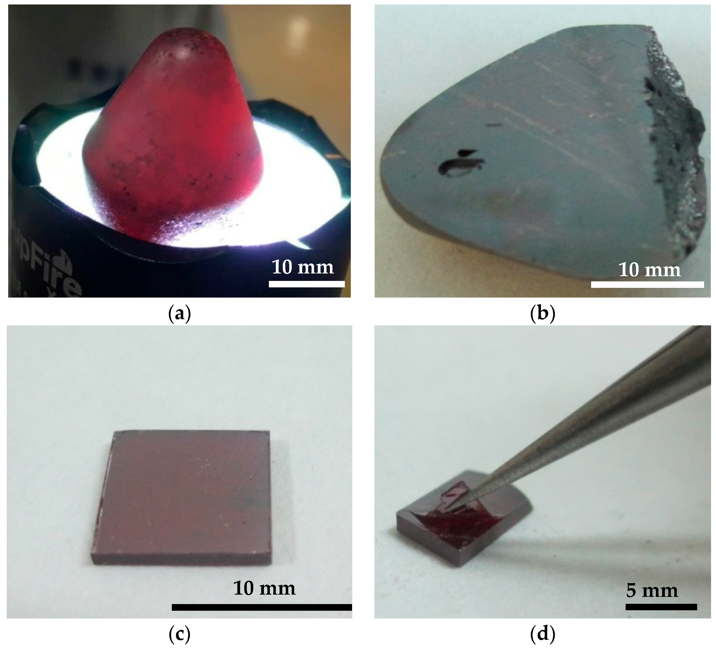
Figure 2.
(a) The powder X-ray diffraction pattern (GaSe) of GaSe sample; (b) the PDF database of GaSe (JCPDS: 37-0931); and (c) the rocking curve of the (004) face.
Figure 2.
(a) The powder X-ray diffraction pattern (GaSe) of GaSe sample; (b) the PDF database of GaSe (JCPDS: 37-0931); and (c) the rocking curve of the (004) face.

Figure 3.
(a) Typical IR transmittance spectrum of a GaSe sample; and (b) the ultraviolet–visible–near IR spectrum of the GaSe sample.
Figure 3.
(a) Typical IR transmittance spectrum of a GaSe sample; and (b) the ultraviolet–visible–near IR spectrum of the GaSe sample.

Figure 4.
Typical PL spectrum of as-grown GaSe crystals at 9.2 K.
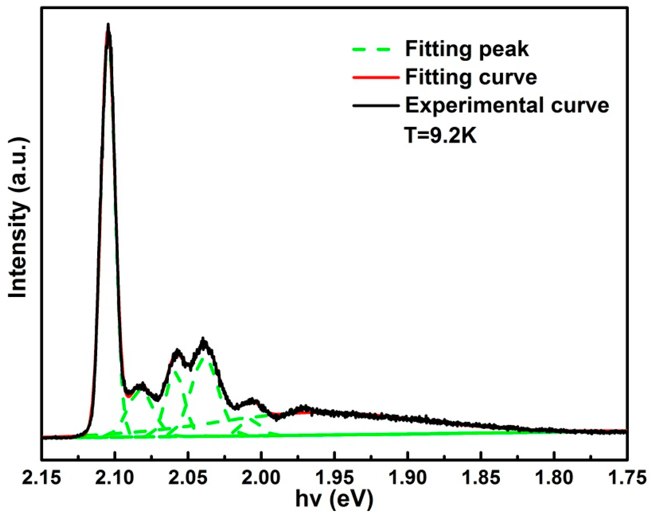
Figure 5.
Few-layered GaSe photo-detector: (a) schematic diagram; (b) optical image; (c) AFM image; (d) AFM height profile along the black line.
Figure 5.
Few-layered GaSe photo-detector: (a) schematic diagram; (b) optical image; (c) AFM image; (d) AFM height profile along the black line.
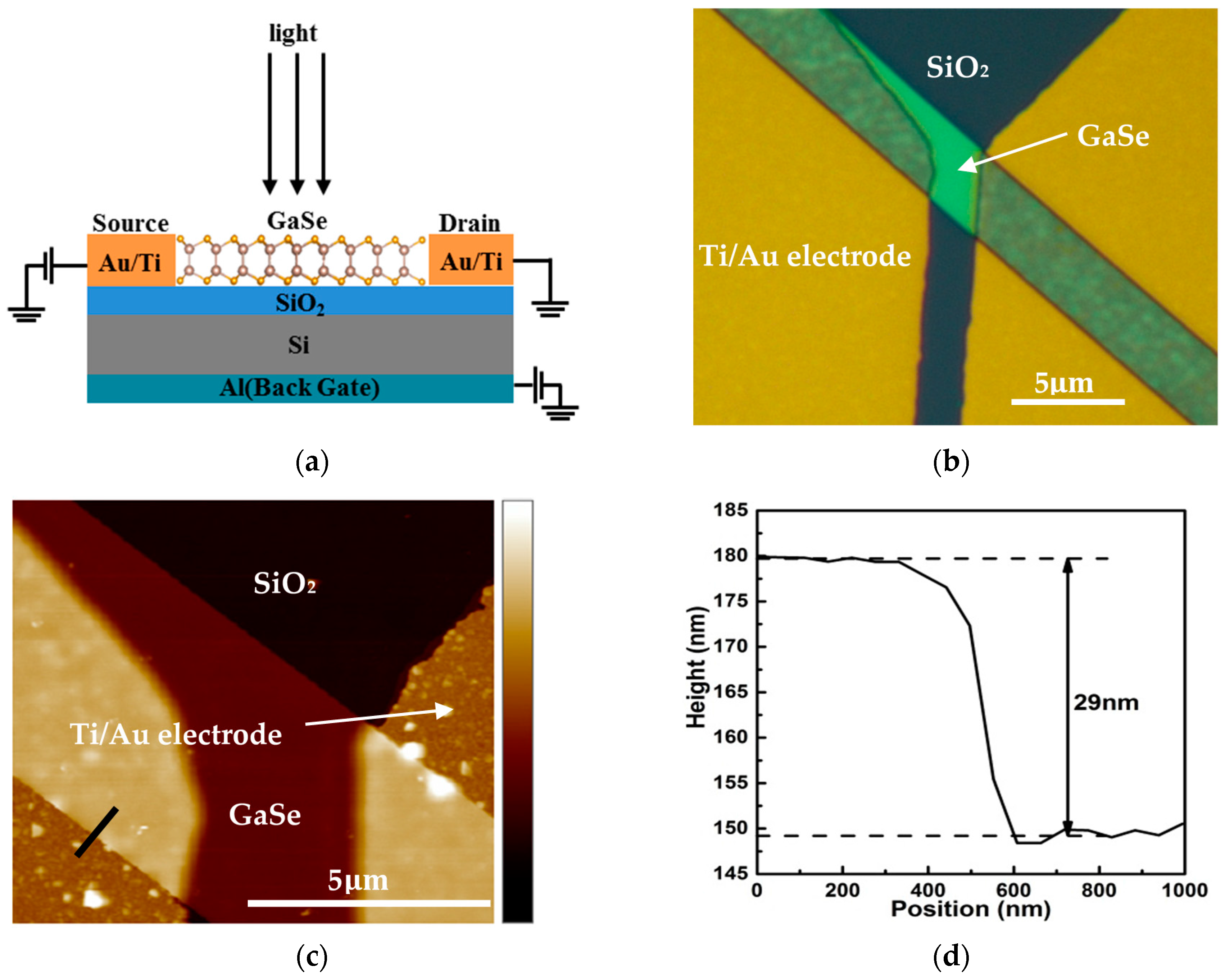
Figure 6.
(a) FET transfer characteristics; (b) output characteristics; (c) photo-response under Vds = −10 V; and (d) time resolved photoresponse in a single period.
Figure 6.
(a) FET transfer characteristics; (b) output characteristics; (c) photo-response under Vds = −10 V; and (d) time resolved photoresponse in a single period.

Table 1.
The composition of GaSe measured by EPMA.
| Sample | Se (Atom %) | Ga (Atom %) |
|---|---|---|
| 1 | 49.5613 | 50.4387 |
| 2 | 49.5203 | 50.4797 |
| 3 | 49.6189 | 50.3811 |
| 4 | 49.5266 | 50.4734 |
Table 2.
The transport properties of GaSe single crystals (T = 295 K).
| Sample | Conductivity Type | Carrier Concentration (cm−3) | Resistivity (Ω·cm) | Mobility (cm2 V−1 s−1) |
|---|---|---|---|---|
| 1 | p | 2.9894 × 10¹⁵ | 1.129546 × 10² | 1.8484 × 101 |
| 2 | p | 1.4701 × 10¹⁵ | 2.332230 × 10² | 1.8204 × 101 |
| 3 | p | 1.6830 × 10¹⁵ | 1.621991 × 10² | 2.3492 × 101 |
© 2018 by the authors. Licensee MDPI, Basel, Switzerland. This article is an open access article distributed under the terms and conditions of the Creative Commons Attribution (CC BY) license (http://creativecommons.org/licenses/by/4.0/).
Share and Cite
MDPI and ACS Style
Wang, T.; Li, J.; Zhao, Q.; Yin, Z.; Zhang, Y.; Chen, B.; Xie, Y.; Jie, W. High-Quality GaSe Single Crystal Grown by the Bridgman Method. Materials 2018, 11, 186. https://doi.org/10.3390/ma11020186
AMA Style
Wang T, Li J, Zhao Q, Yin Z, Zhang Y, Chen B, Xie Y, Jie W. High-Quality GaSe Single Crystal Grown by the Bridgman Method. Materials. 2018; 11(2):186. https://doi.org/10.3390/ma11020186
Chicago/Turabian StyleWang, Tao, Jie Li, Qinghua Zhao, Ziang Yin, Yinghan Zhang, Bingqi Chen, Yong Xie, and Wanqi Jie. 2018. "High-Quality GaSe Single Crystal Grown by the Bridgman Method" Materials 11, no. 2: 186. https://doi.org/10.3390/ma11020186
Note that from the first issue of 2016, this journal uses article numbers instead of page numbers. See further details here.