Interface Tailoring Effect for Heusler Based CPP-GMR with an L12-Type Ag3Mg Spacer


1
Institute for Materials Research, Tohoku University, Sendai 980-8577, Japan
2
Center for Spintronics Research Network, Tohoku University, Sendai 980-8577, Japan
*
Author to whom correspondence should be addressed.
Materials 2018, 11(2), 219; https://doi.org/10.3390/ma11020219
Submission received: 31 December 2017
/
Revised: 19 January 2018
/
Accepted: 29 January 2018
/
Published: 31 January 2018
(This article belongs to the Special Issue Magnetoresistance Effects and Their Application to Spintronic Devices)
Abstract
:Current perpendicular-to-plane (CPP) giant magnetoresistance (GMR) effects are of interest in a possible application of magnetic sensor elements, such as read-head of hard disk drives. To improve the junction performance, the interface tailoring effects were investigated for the Heulser alloy, Co2Fe0.4Mn0.6Si (CFMS), based CPP-GMR junctions with an -Ag3Mg ordered alloy spacer. Ultra-thin Fe or Mg inserts were utilized for the CFMS/Ag3Mg interfaces, and CPP-GMR at low bias current density, J and the J dependence were evaluated for the junctions. Although, at low bias J, MR ratio decreased with increasing the inserts thickness, the device output at high bias J exhibited quite weak dependence on the insert thickness. The output voltages of the order of 4 mV were obtained for the junctions regardless of the insert at an optimal bias J for each. The critical current density was evaluated by the shape of MR curves depending on J. increased with the insert thicknesses up to 0.45 nm. The enhancement of suggests that spin-transfer-torque effect may reduce in the junctions with inserts, which enables a reduction of noise and can be an advantage for device applications.
1. Introduction
Current perpendicular to plane (CPP) giant magnetoresistance (GMR) junction is potentially utilized for highly sensitive magnetic sensor applications, e.g., read-head devices for hard disk drives (HDDs) [1,2,3,4]. A merit of CPP-GMR junction is a relatively low areal resistance () of the order of 10−2–10−3·m2, which is an advantage over tunnel magnetoresistance (TMR) junctions. The low in the optimum range applicable to the next generation HDDs with areal recording density of several tera-bit-per-square-inches [3]. Magnetic tunnel junctions (MTJs) with an MgO barrier exhibit a high MR ratio over 100% with down to 1 ·m2 [5,6]; however, the MR ratio decreases for a lower region because of the ultra-thin tunneling barrier. The reduction of the MR with the reduced barrier thickness is unavoidable from the principle of coherent tunneling [7,8]. Thus, we can say that an advantage of CPP-GMR is the low compared to MgO-MTJs, which is currently used for HDD read-heads, and the development of CPP-GMR is necessary for futre HDD tecnology. According to the theoretical model proposed by Valet and Fert in 1993 [9], spin asymmetry coefficients crucially affect the resistance change of CPP-GMR junctions, which are defined by magnetic material as well as the interface between a non-magnetic spacer and the magnetic layer. For realization of high output for the CPP-GMR junctions, magnetic materials with high-spin polarization are essential. One of the developed magnetic material classes for CPP-GMR junctions is half-metallic cobalt (Co)-based Heusler alloys for some of which the theoretically predicted spin polarization is 100% [10]. In experiments for CPP-GMR, a pioneer work has been reported for junctions using Co2MnSi Heusler alloy and a Cr spacer, in which relatively large resistance change was observed [11]. The next trigger was given by a Ag spacer for the Co2-Heusler junctions, in which MR ratio and the areal resistance change () reached to about 30% and 10 m·m2, respectively, at room temperature [12,13]. To date, several Heusler alloys are known as half-metallic and have been utilized for CPP-GMR junctions, e.g., Co2(Al-Si) [13,14], Co2MnGe [15,16], Co2(Fe-Mn)Si [17,18], and Co2(Ga-Ge) [19]. Selection of the spacer material is another crucial factor for CPP-GMR from a viewpoint of band-dispersion-matching to the Heusle alloy layers [20,21,22,23], for the purpose of which various non-magnetic materials have also been investigated experimentally, e.g., Cr, Ag, Cu, non-magnetic Heusler alloys [20,24,25], -type NiAl [26], noble-metal(Cu or Ag)-Zn alloys [27,28], conductive oxide [29], and so on.
Among the numerous materials we have focused on a Co2Fe0.4Mn0.6Si (CFMS) alloy as a half-metallic material, and an Ag3Mg alloy as a spacer, for which schematic crystal structures are shown in Figure 1a,b, respectively. CFMS is a known half-metallic material on the bases of both theoretical and experimental studies [18,30,31]. One of the merits is a high exchange stiffness at the interface which is important for realizing large CPP-GMR at room temperature [32,33]. The Ag3Mg is an ordered alloy spacer material for which good band-dispersion-matching to CFMS has been predicted [34], and large CPP-GMR have experimentally demonstrated for CFMS/ Ag3Mg/CFMS junctions, which is an advantage over the Ag spacer junctions [34,35,36].
In this work, the interface tailoring effect is investigated for the CFMS/ Ag3Mg/CFMS junctions to improve the output performance. According to literatures [37,38], ultra-thin inserts at Heusler layer/spacer interfaces drastically modified the CPP-GMR properties. For the insert materials, Fe and Mg have been selected. The Fe insert is interested in enhancing the exchange stiffness at the interface [33,38], and the Mg insert is interesting because the electronic state consists of -components only [39], which may result in a filtering effect for the highly spin polarized electrons of Heusler alloys with -like symmetry.
2. Materials and Methods
Layered films were deposited onto MgO (100) single crystalline substrates by using an ultra-high vacuum magnetron sputtering system for which base pressure of the vacuum chamber was less than 1 × 10⁻⁷ Pa. For the sputtering power sources, radio frequency source was used for the Ag target, and direct current source was used for other targets. The stacking structure of samples is as follows and shown in Figure 1c: Cr (20 nm) | Ag (40 nm) | CFMS (20 nm) | Fe or Mg () | Ag3Mg (5 nm) | Fe or Mg () | CFMS (7 nm) | Ag (2 nm) | Au (5 nm), from bottom to top. The film compositions of the CFMS and Ag3Mg layeres were Co47Fe13Mn15Si25 (at.%) and Ag78Mg22 (at.%), respectively. The thicknesses for the inserts, , ranged from 0 to 0.6 nm in 0.15 nm increments. The surface of the MgO substrates was flushed at 650 °C by using an infrared heater equipped inside the ultra-high vacuum chamber. All layeres were deposited at room temperature and in situ post-annealing was carried out at 650 and 550 °C after the deposition of the Cr and the upper CFMS layer, respectively. Crystalline property of the films was examined using reflection high energy electron diffraction, RHEED, patterns for the surface of the upper CFMS electrode. The layered films were patterned into a pillar shape with sub-micrometer-scale using electron-beam lithography and argon ion dry etching technique. Designed pillar sizes ranged from 50 × 100 nm2 to 400 × 800 nm2 with a rectangular shape. And actual pillar sizes were estimated using the same method as that in our previous studies [34,40], which ranged from 40 × 80 nm2 to 390 × 780 nm2, approximately. The values of junctions were estimated using resistance at the parallel magnetization configuration, , as a function of the inverse junction area, , where A is in the unit of m2. The measuerments of were carried out for all sizes of junctions. The detail for the procedure of estimation was described in a previous paper of ours [36]. CPP-GMR effects were measured by four-probe method at room temperature. In this paper CPP-GMR effects were characterized by two aspects: CPP-GMR effects at low bias current density, J and the bias J dependence of CPP-GMR. For the measurements at low J, the current was fixed so that the applied bias voltage was about 1 mV at a parallel magnetization configuration, and the magnetic field was swept along a long axis of the pillar shape which is an easy magnetization axis. Regarding the value of MR ratio, two definitions are used: The observed MR ratio, MRobs, and the intrinsic MR ratio, MRint, for which the parasitic resistance, was subtracted from , where represents the junction resistance at antiparallel magnetization configuration. Here, originates from the resistance of the lead electrodes for the junction. The values are defined by the following equations;
And is also defined as follows;
For the J dependence, GMR curves were measured at several values of J within the range of about 108 A/cm2, and the magnetic field was swept along a short axis of the pillar shape, which is a hard magnetization axis direction.
3. Results and Discussion
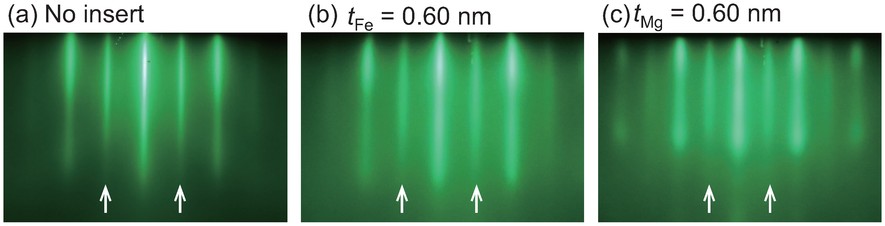
RHEED images are shown in Figure 2 for the surface of the upper CFMS layer in the layered films for CFMS<110> azimuth. The thickness of the inserts is 0.6 nm for Fe (Figure 2b) or Mg (Figure 2c), which is the maximum thickness of the inserts among the samples. Regardless of the inserts, streaks are clearly observed including the superlattice streaks from the phase of the CFMS layer which are pointed by arrows. RHEED images for another azimuth of CFMS<100> also showed streak patterns including the fundamental diffractions only (not shown here). RHEED images for other insert-thicknesses samples also showed similar features. Thus, it is confirmed that the epitaxial growth and the phase in the CFMS electrode are maintained for all samples including the samples with Fe or Mg inserts.
Summaries of , , and MR ratios at low bias J are shown in Figure 3a,d, Figure 3b,e and Figure 3c,f, respectively. Figure 3a–f indicate the inserts thickness dependence of the junctions with the Fe inserts and the Mg inserts, respectively. The error bars represent the standard deviation estimated from the measured junctions.
Regarding the junctions with Fe inserts, the value slightly increases with of up to 0.45 nm and decreases for of 0.60 nm. Both and MR ratios monotonically decrease with increasing . Although the reason for the dependence is unclear, a change of band-matching is a possible factor caused by the inserts [23,37]. On the other hand, regarding the junctions with Mg inserts, , and MR ratios exhibit smaller values than those for junctions with no insert . For the junctions with Mg inserts, and MR ratios show non-monotonic decrease, which is different from junctions with Fe inserts . The difference between the Fe and Mg inserts is discussed as follows: Firstly the Fe inserts possibly formed an alloy with the CFMS layer by annealing at 550 °C. Assuming that the interfaces became Fe-rich CFMS, the spin polarization was smaller than that of the original CFMS composition, which was reported by Sakuraba et al. [18]. Even in case that the Fe layers remained at the interfaces, the spin polarization would be smaller than that of the original CFMS/Ag3Mg interfaces, which is similar with a work done by Jung et al. [38]. On the other hand for the Mg inserts, the Mg possibly remained as Mg-layeres at the CFMS/Ag3Mg interfaces, because Mg atoms are less soluble with the CFMS layers, which was discussed in a previous paper of ours [36]. The and the MR ratios decrease due to the reduced interface spin asymmetry at the Mg interfaces. Concerning the non-monotonic decrease for the and the MR ratios, a conduction channel through the quantum states in the ultra-thin Mg layer is a possible factor [39].
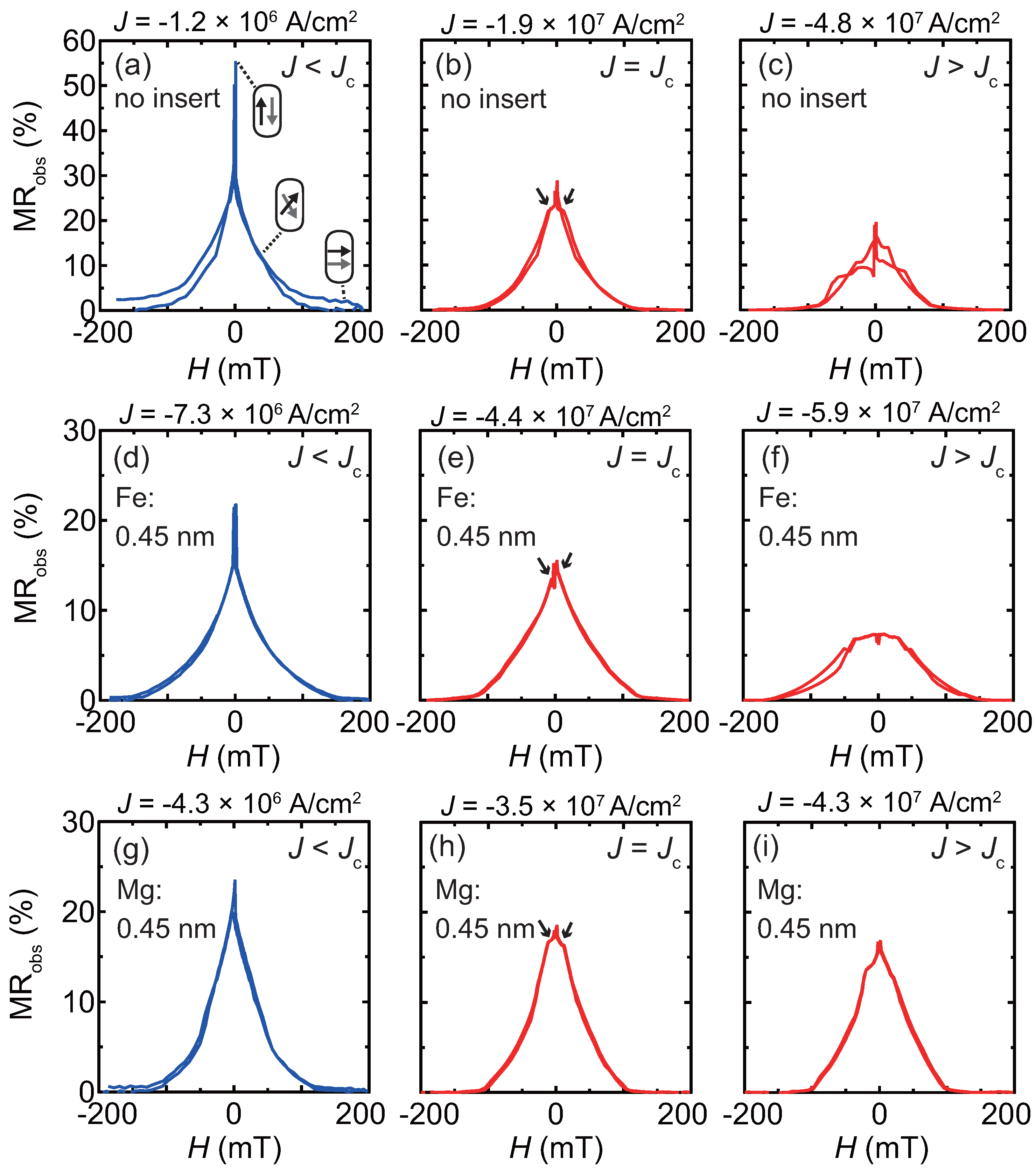
Figure 4 shows typical MR curves for the investigation of bias J dependence, the shapes of which are explained as follows for the low bias region, : Firstly, magnetizations of the CFMS layers are coupled with antiferromagnetically through the dipolar field from the pillar edges, thus the MR ratios exhibit a maximum value at the zero magnetic field, . With increasing H, magnetizations gradually rotate, the behavior of which is similar with that of the edges of scissors schematically illustrated by arrows in Figure 4a. By applying sufficiently large H, e.g., 200 mT, magnetizations aligned in parallel configuration and the junction resistance becomes a minimum. A similar shape of MR curve was reported in the literature for a Heusler alloy based CPP-GMR with antiferromagentic coupling [41].
From the shape of MR curves, the critical current density, , is defined at the point where small shoulders start to appear in the MR curve. The shoulders are pointed by arrows in Figure 4b, Figure 4e and Figure 4h for junctions with no insert, 0.45 nm-thick Fe inserts, and 0.45 nm-thick Mg insert, respectively. For , the shapes of MR curves collapse because of the unstable antiparallel configuration of the magnetization which were fluctuated by spin-transfer torque (the curves are shown in Figure 4c, Figure 4f and Figure 4i for no insert, the Fe inserts, and Mg inserts junctions, respectively).
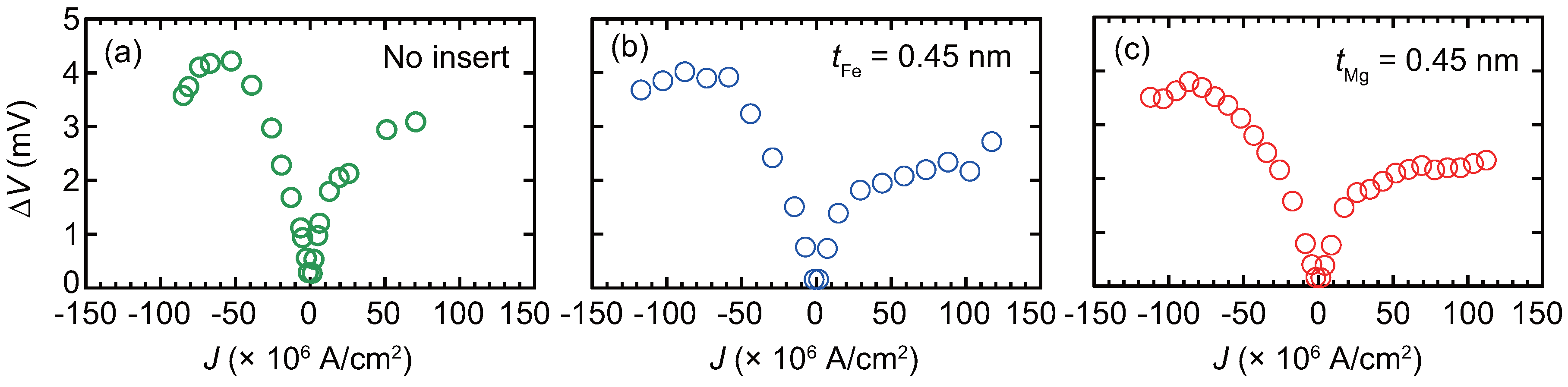
The J dependence of the output voltage () is shown in Figure 5 for a junction with no insert and junctions with 0.45 nm-thick Fe or Mg inserts. Here is defined by the following equation:
where , , and represent the maximum resistance in the MR curve, resistance at mT, and the bias current for the measured MR curve, respectively. The positive bias is defined by the electron flow from the bottom to top. The for each data point was obtained by sweeping an MR curve at a bias J, for which examples are shown in Figure 4. shows asymmetric dependence on J, because the volume of the upper CFMS layer is smaller than that of the bottom: Considering the effect of spin-transfer-torque (STT), the parallel magnetization configuration is stabilized by the electron flow for the positive bias, while the antiparallel configuration is stabilized for the negative bias. exhibits a maximum value at J at around −90–−50 A/cm2, which is defined as .
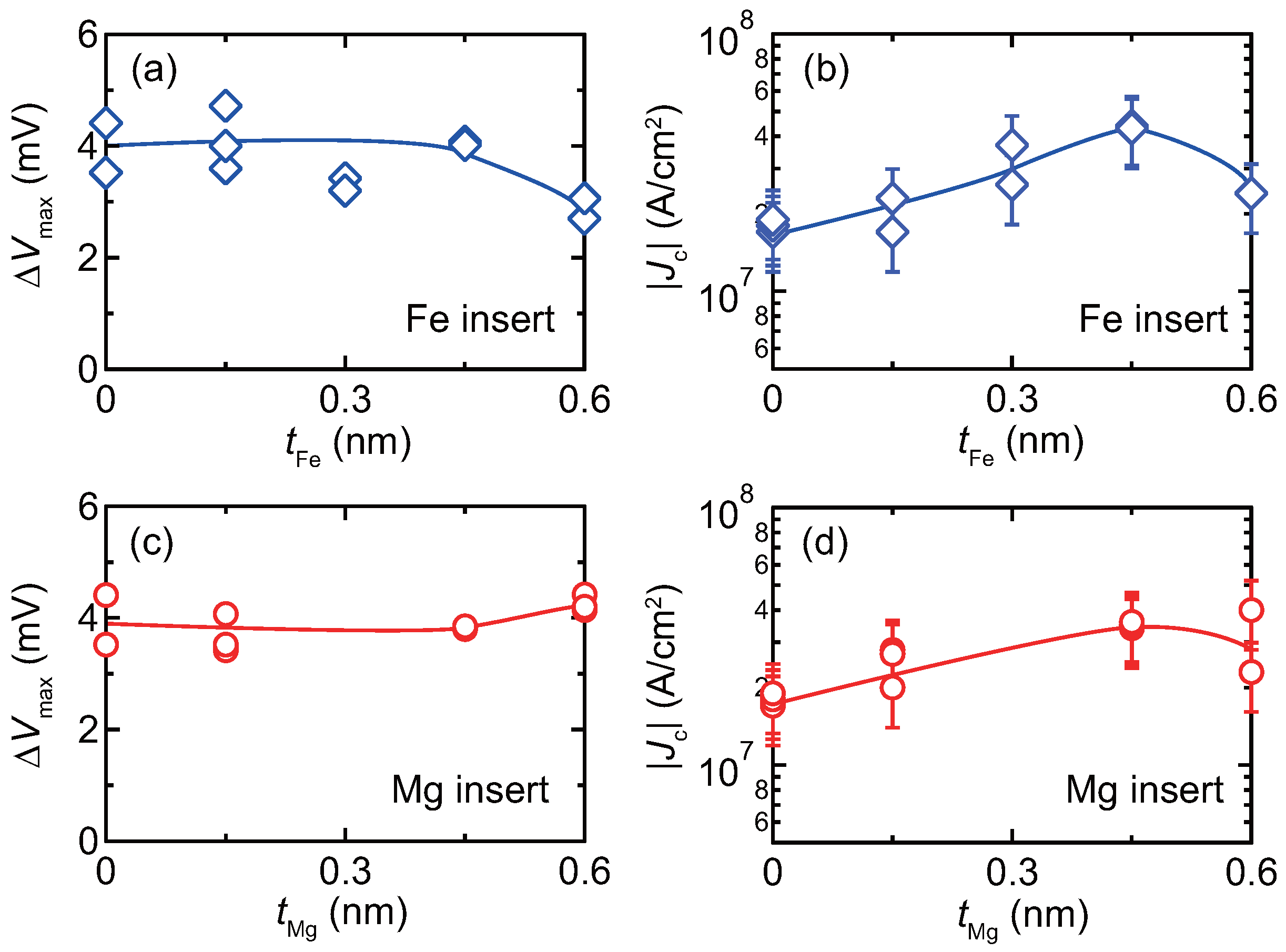
Summaries of and as a function of the insert thickness, are shown in Figure 6. For the Fe insert junctions, of the order of 4 mV is obtained for in the range of 0.45 nm, and the value drops to about 3 mV for = 0.60 nm. For the Mg insert junctions, is almost independent of and the values are about 4 mV. Regarding the dependence of , the values increase with the insert thickness of up to 0.45 nm for the Fe insert junctions and decreases at 0.60 nm, which is similar to the dependence for the Mg insert junctions. The increase of can be qualitatively explained that the STT effect reduced because of the reduced spin polarization which correlates with MR ratio. In addition, for the case of the Fe insert junctions, enhancement of Gilbert damping constant is another possible factor [42,43], which enhances torque acting towards opposite direction to that of the STT [44]. Although MR ratio was degraded at low bias J by the inserts, almost unchanged because of the balance between the spin polarization and the STT effect. Considering CPP-GMR for read head application of HDDs, the noise caused by STT is an issue to be suppressed [3]. From the bias J dependence for the present junctions, it is suggested for the junction with inserts that the can be maintained under a condition with smaller STT effect. Such a device feature is favorable for the read head or similar sensor applications.
4. Conclusions
Interface tailoring effect was investigated for the CPP-GMR junctions including the CFMS/Ag3Mg/CFMS structure with the ultra-thin Fe or Mg inserts. Epitaxially grown layered structures were successfully fabricated including the samples with the Fe or Mg inserts of the thickness up to 0.60 nm. At low bias J, MR ratio decreased with the insert thickness. On the other hand, the junctions output was almost unchanged by the inserts, which was of the order of 4 mV. These trends were similar between the junctions using Fe and Mg inserts. The inserts possibly suppressed the STT effect, resulting in the relatively large at the large bias J. The suppressed STT is considered as a merit of the insert for CPP-GMR junctions for device applications.
Acknowledgments
This work was partially supported by Grant-in-Aid for Scientific Research(S), Grant No. 25220910, from the Japan Society for the Promotion of Science, and Advanced Storage Research Consortium (ASRC). This work was a part of a cooperative program (Grant No. 17G0409) of the CRDAM-IMR, Tohoku University.
Author Contributions
Takahide Kubota and Koki Takanashi conceived and designed the experiments; Takahide Kubota and Yusuke Ina performed the experiments; all authors analyzed and discussed the data; Takahide Kubota, Zhenchao Wen and Koki Takanashi wrote the paper. Authorship must be limited to those who have contributed substantially to the work reported.
Conflicts of Interest
The authors declare no conflict of interest.
References
- Takagishi, M.; Koi, K.; Yoshikawa, M.; Funayama, T.; Iwasaki, H.; Sahashi, M. The applicability of CPP-GMR heads for magnetic recording. IEEE Trans. Magn. 2002, 38, 2277–2282. [Google Scholar] [CrossRef]
- Childress, J.R.; Carey, M.J.; Maat, S.; Smith, N.; Fontana, R.E.; Druist, D.; Carey, K.; Katine, J.A.; Robertson, N.; Boone, T.D.; et al. All-Metal Current-Perpendicular-to-Plane Giant Magnetoresistance Sensors for Narrow-Track Magnetic Recording. IEEE Trans. Magn. 2008, 44, 90–94. [Google Scholar] [CrossRef]
- Takagishi, M.; Yamada, K.; Iwasaki, H.; Fuke, H.N.; Hashimoto, S. Magnetoresistance Ratio and Resistance Area Design of CPP-MR Film for 2–5 Tb/in2 Read Sensors. IEEE Trans. Magn. 2010, 46, 2086–2089. [Google Scholar] [CrossRef]
- Hirohata, A.; Sukegawa, H.; Yanagihara, H.; Zutic, I.; Seki, T.; Mizukami, S.; Swaminathan, R. Roadmap for Emerging Materials for Spintronic Device Applications. IEEE Trans. Magn. 2015, 51, 1–11. [Google Scholar] [CrossRef]
- Nagamine, Y.; Maehara, H.; Tsunekawa, K.; Djayaprawira, D.D.; Watanabe, N.; Yuasa, S.; Ando, K. Ultralow resistance-area product of 0.4 Ωμm2 and high magnetoresistance above 50% in CoFeB/MgO/CoFeB magnetic tunnel junctions. Appl. Phys. Lett. 2006, 89, 162507. [Google Scholar] [CrossRef]
- Maehara, H.; Nishimura, K.; Nagamine, Y.; Tsunekawa, K.; Seki, T.; Kubota, H.; Fukushima, A.; Yakushiji, K.; Ando, K.; Yuasa, S. Tunnel Magnetoresistance above 170% and Resistance–Area Product of 1 Ω(μm)2 Attained by In situ Annealing of Ultra-Thin MgO Tunnel Barrier. Appl. Phys. Express 2011, 4, 033002. [Google Scholar] [CrossRef]
- Butler, W.H.; Zhang, X.G.; Schulthess, T.C.; MacLaren, J.M. Spin-dependent tunneling conductance of Fe|MgO|Fe sandwiches. Phys. Rev. B 2001, 63, 054416. [Google Scholar] [CrossRef]
- Mathon, J.; Umerski, A. Theory of tunneling magnetoresistance of an epitaxial Fe/MgO/Fe(001) junction. Phys. Rev. B 2001, 63, 220403. [Google Scholar] [CrossRef]
- Valet, T.; Fert, A. Theory of the perpendicular magnetoresistance in magnetic multilayers. Phys. Rev. B 1993, 48, 7099–7113. [Google Scholar] [CrossRef]
- Felser, C.; Fecher, G.; Balke, B. Spintronics: A Challenge for Materials Science and Solid-State Chemistry. Angew. Chem. Int. Ed. 2007, 46, 668–699. [Google Scholar] [CrossRef] [PubMed]
- Yakushiji, K.; Saito, K.; Mitani, S.; Takanashi, K.; Takahashi, Y.K.; Hono, K. Current-perpendicular-to-plane magnetoresistance in epitaxial Co2MnSiCrCo2MnSi trilayers. Appl. Phys. Lett. 2006, 88, 222504. [Google Scholar] [CrossRef]
- Iwase, T.; Sakuraba, Y.; Bosu, S.; Saito, K.; Mitani, S.; Takanashi, K. Large Interface Spin-Asymmetry and Magnetoresistance in Fully Epitaxial Co2MnSi/Ag/Co2MnSi Current-Perpendicular-to-Plane Magnetoresistive Devices. Appl. Phys. Express 2009, 2, 063003. [Google Scholar] [CrossRef]
- Furubayashi, T.; Kodama, K.; Sukegawa, H.; Takahashi, Y.K.; Inomata, K.; Hono, K. Current-perpendicular-to-plane giant magnetoresistance in spin-valve structures using epitaxial Co2FeAl0.5Si0.5/Ag/Co2FeAl0.5Si0.5 trilayers. Appl. Phys. Lett. 2008, 93, 122507. [Google Scholar] [CrossRef]
- Nakatani, T.M.; Furubayashi, T.; Kasai, S.; Sukegawa, H.; Takahashi, Y.K.; Mitani, S.; Hono, K. Bulk and interfacial scatterings in current-perpendicular-to-plane giant magnetoresistance with Co2Fe(Al0.5Si0.5) Heusler alloy layers and Ag spacer. Appl. Phys. Lett. 2010, 96, 212501. [Google Scholar] [CrossRef]
- Maat, S.; Carey, M.J.; Childress, J.R. Current perpendicular to the plane spin-valves with CoFeGe magnetic layers. Appl. Phys. Lett. 2008, 93, 143505. [Google Scholar] [CrossRef]
- Carey, M.J.; Maat, S.; Chandrashekariaih, S.; Katine, J.A.; Chen, W.; York, B.; Childress, J.R. Co2MnGe-based current-perpendicular-to-the-plane giant-magnetoresistance spin-valve sensors for recording head applications. J. Appl. Phys. 2011, 109, 093912. [Google Scholar]
- Sato, J.; Oogane, M.; Naganuma, H.; Ando, Y. Large Magnetoresistance Effect in Epitaxial Co2Fe0.4Mn0.6Si/ Ag/Co2Fe0.4Mn0.6Si Devices. Appl. Phys. Express 2011, 4, 113005. [Google Scholar] [CrossRef]
- Sakuraba, Y.; Ueda, M.; Miura, Y.; Sato, K.; Bosu, S.; Saito, K.; Shirai, M.; Konno, T.J.; Takanashi, K. Extensive study of giant magnetoresistance properties in half-metallic Co2(Fe,Mn)Si-based devices. Appl. Phys. Lett. 2012, 101, 252408. [Google Scholar] [CrossRef]
- Li, S.; Takahashi, Y.K.; Furubayashi, T.; Hono, K. Enhancement of giant magnetoresistance by L21 ordering in Co2Fe(Ge0.5Ga0.5) Heusler alloy current-perpendicular-to-plane pseudo spin valves. Appl. Phys. Lett. 2013, 103, 042405. [Google Scholar] [CrossRef]
- Nikolaev, K.; Kolbo, P.; Pokhil, T.; Peng, X.; Chen, Y.; Ambrose, T.; Mryasov, O. “All-Heusler alloy” current-perpendicular-to-plane giant magnetoresistance. Appl. Phys. Lett. 2009, 94, 222501. [Google Scholar] [CrossRef]
- Ko, V.; Han, G.; Qiu, J.; Feng, Y.P. The band structure-matched and highly spin-polarized Co2CrZ/Cu2CrAl Heusler alloys interface. Appl. Phys. Lett. 2009, 95, 202502. [Google Scholar] [CrossRef]
- Sakuraba, Y.; Izumi, K.; Iwase, T.; Bosu, S.; Saito, K.; Takanashi, K.; Miura, Y.; Futatsukawa, K.; Abe, K.; Shirai, M. Mechanism of large magnetoresistance in Co2MnSi/Ag/Co2MnSi devices with current perpendicular to the plane. Phys. Rev. B 2010, 82, 09444. [Google Scholar] [CrossRef]
- Miura, Y.; Futatsukawa, K.; Nakajima, S.; Abe, K.; Shirai, M. First-principles study of ballistic transport properties in Co2MnSi/X/Co2MnSi(001) (X = Ag, Au, Al, V, Cr) trilayers. Phys. Rev. B 2011, 84, 134432. [Google Scholar] [CrossRef]
- Kubota, T.; Oogane, M.; Mizukami, S.; Naganuma, H.; Ando, Y.; Miyazaki, T. Magnetoresistance Effect in Co2MnSi/semimetallic-Fe2VAl/CoFe Junctions. J. Phys. Conf. Ser. 2011, 266, 012096. [Google Scholar] [CrossRef]
- Li, S.; Takahashi, Y.K.; Sakuraba, Y.; Chen, J.; Furubayashi, T.; Mryasov, O.; Faleev, S.; Hono, K. Current-perpendicular-to-plane giant magnetoresistive properties in Co2Mn(Ge0.75Ga0.25)/Cu2TiAl/Co2Mn (Ge0.75Ga0.25) all-Heusler alloy pseudo spin valve. J. Appl. Phys. 2016, 119, 093911. [Google Scholar]
- Hase, N.; Nakatani, T.; Kasai, S.; Takahashi, Y.; Furubayashi, T.; Hono, K. Effect of NiAl underlayer and spacer on magnetoresistance of current-perpendicular-to-plane spin valves using Co2Mn(Ga0.5Sn0.5) Heusler alloy. J. Magn. Magn. Mater. 2012, 324, 440–444. [Google Scholar] [CrossRef]
- Furubayashi, T.; Takahashi, Y.K.; Sasaki, T.T.; Hono, K. Enhancement of current-perpendicular-to-plane giant magnetoresistance in Heusler-alloy based pseudo spin valves by using a CuZn spacer layer. J. Appl. Phys. 2015, 118, 163901. [Google Scholar] [CrossRef]
- Li, S.; Nakatani, T.; Masuda, K.; Sakuraba, Y.; Xu, X.; Sasaki, T.; Tajiri, H.; Miura, Y.; Furubayashi, T.; Hono, K. Enhancement of current-perpendicular-to-plane giant magnetoresistive outputs by improving B2-order in polycrystalline Co2(Mn0.6Fe0.4)Ge Heusler alloy films with the insertion of amorphous CoFeBTa underlayer. Acta Mater. 2018, 142, 49–57. [Google Scholar] [CrossRef]
- Nakatani, T.; Mihajlović, G.; Read, J.C.; Suk Choi, Y.; Childress, J.R. High signal output in current-perpendicular- to-the-plane giant magnetoresistance sensors using In-Zn-O-based spacer layers. Appl. Phys. Express 2015, 8, 093003. [Google Scholar]
- Balke, B.; Fecher, G.H.; Kandpal, H.C.; Felser, C.; Kobayashi, K.; Ikenaga, E.; Kim, J.J.; Ueda, S. Properties of the quaternary half-metal-type Heusler alloy Co2Mn1-xFexSi. Phys. Rev. B 2006, 74, 104405. [Google Scholar] [CrossRef]
- Kubota, T.; Tsunegi, S.; Oogane, M.; Mizukami, S.; Miyazaki, T.; Naganuma, H.; Ando, Y. Half-metallicity and Gilbert damping constant in Co2FexMn1-xSi Heusler alloys depending on the film composition. Appl. Phys. Lett. 2009, 94, 122504. [Google Scholar] [CrossRef]
- Sakuraba, Y.; Ueda, M.; Bosu, S.; Saito, K.; Takanashi, K. CPP-GMR study of half-metallic full-Heusler compound Co2(Fe,Mn)Si. J. Magn. Soc. Jpn. 2014, 38, 45–49. [Google Scholar] [CrossRef]
- Yako, H.; Sakuraba, Y.; Amemiya, K.; Sakamaki, M.; Kubota, T.; Sasaki, T.; Miura, Y.; Hono, K.; Takanashi, K. Investigation of the exchange stiffness at Co2MnSi/Ag and Co2FeSi/Ag interfaces using the depth-resolved X-ray magnetic circular dichroism. In Proceedings of the 59th Annual Conference on Magnetism and Magnetic Materials, Honolulu, HI, USA, 3–7 November 2014; p. EP–13. [Google Scholar]
- Kubota, T.; Ina, Y.; Tsujikawa, M.; Morikawa, S.; Narisawa, H.; Wen, Z.; Shirai, M.; Takanashi, K. Current perpendicular-to-plane giant magnetoresistance devices using half-metallic Co2Fe0.4Mn0.6Si electrodes and a Ag-Mg spacer. J. Phys. D Appl. Phys. 2016, 50, 014004. [Google Scholar] [CrossRef]
- Narisawa, H.; Kubota, T.; Takanashi, K. Current perpendicular to film plane type giant magnetoresistance effect using a Ag-Mg spacer and Co2Fe0.4Mn0.6Si Heusler alloy electrodes. Appl. Phys. Express 2015, 8, 063008. [Google Scholar] [CrossRef]
- Kubota, T.; Ina, Y.; Wen, Z.; Narisawa, H.; Takanashi, K. Current perpendicular-to-plane giant magnetoresistance using an L12 Ag3Mg spacer and Co2Fe0.4Mn0.6Si Heusler alloy electrodes: Spacer thickness and annealing temperature dependence. Phys. Rev. Mater. 2017, 1, 044402. [Google Scholar] [CrossRef]
- Jung, J.W.; Sakuraba, Y.; Sasaki, T.T.; Miura, Y.; Hono, K. Enhancement of magnetoresistance by inserting thin NiAl layers at the interfaces in Co2FeGa0.5Ge0.5/Ag/Co2FeGa0.5Ge0.5 current-perpendicular-to-plane pseudo spin valves. Appl. Phys. Lett. 2016, 108, 102408. [Google Scholar] [CrossRef]
- Jung, J.W.; Sakuraba, Y.; Bosu, S.; Li, S.; Hono, K. Enhancement of Interfacial Spin-Dependent Scattering of Co2Fe(Ga0.5Ge0.5)/Ag/Co2Fe(Ga0.5Ge0.5) Current-Perpendicular-to-Plane Giant Magnetoresistive Pseudo-Spin Valves. IEEE Trans. Magn. 2016, 52, 1–4. [Google Scholar] [CrossRef]
- Aballe, L.; Rogero, C.; Horn, K. Quantum-size effects in ultrathin Mg films: Electronic structure and collective excitations. Surf. Sci. 2002, 518, 141–154. [Google Scholar] [CrossRef]
- Narisawa, H.; Kubota, T.; Takanashi, K. Reply to “Comment on ‘Current perpendicular to film plane type giant magnetoresistance effect using a Ag-Mg spacer and Co2Fe0.4Mn0.6Si Heusler alloy electrodes”. Appl. Phys. Express 2015, 8, 119102. [Google Scholar] [CrossRef]
- Nakatani, T.M.; Mitani, S.; Furubayashi, T.; Hono, K. Oscillatory antiferromagnetic interlayer exchange coupling in Co2Fe(Al0.5Si0.5)/Ag/Co2Fe(Al0.5Si0.5) films and its application to trilayer magnetoresistive sensor. Appl. Phys. Lett. 2011, 99, 182505. [Google Scholar] [CrossRef]
- Oogane, M.; Kubota, T.; Kota, Y.; Mizukami, S.; Naganuma, H.; Sakuma, A.; Ando, Y. Gilbert magnetic damping constant of epitaxially grown Co-based Heusler alloy thin films. Appl. Phys. Lett. 2010, 96, 252501. [Google Scholar] [CrossRef]
- Oogane, M.; Wakitani, T.; Yakata, S.; Yilgin, R.; Ando, Y.; Sakuma, A.; Miyazaki, T. Magnetic Damping in Ferromagnetic Thin Films. Jpn. J. Appl. Phys. 2006, 45, 3889–3891. [Google Scholar] [CrossRef]
- Slonczewski, J. Current-driven excitation of magnetic multilayers. J. Magn. Magn. Mater. 1996, 159, L1–L7. [Google Scholar] [CrossRef]
Figure 1.
Schematic illustrations of crystal structures for (a) Co2(Fe,Mn)Si (CFMS) full Heusler alloy in the phase; (b) Ag3Mg alloy in the phase, and (c) stacking structure of the layered films for current perpendiculr to plane (CPP) giant magnetoresistance (GMR) junctions.
Figure 1.
Schematic illustrations of crystal structures for (a) Co2(Fe,Mn)Si (CFMS) full Heusler alloy in the phase; (b) Ag3Mg alloy in the phase, and (c) stacking structure of the layered films for current perpendiculr to plane (CPP) giant magnetoresistance (GMR) junctions.
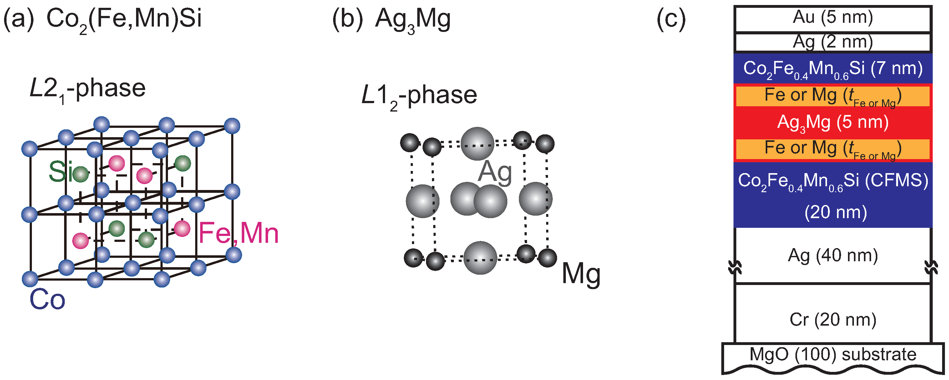
Figure 2.
Reflection high-energy electron diffraction (RHEED) images for the surface of the upper CFMS layer for azimuth of CFMS <110>. Layered films with (a) no insert; (b) Fe inserts of 0.60 nm, and (c) Mg inserts of 0.60 nm. The arrows indicate the superlattice streaks from the phase of CFMS.
Figure 2.
Reflection high-energy electron diffraction (RHEED) images for the surface of the upper CFMS layer for azimuth of CFMS <110>. Layered films with (a) no insert; (b) Fe inserts of 0.60 nm, and (c) Mg inserts of 0.60 nm. The arrows indicate the superlattice streaks from the phase of CFMS.

Figure 3.
A summary of the insert thickness dependence of CPP-GMR at low bias current density for junctions with (a–c) Fe inserts and (d–f) Mg insert. (a,d) , (b,e) , and (c,f) MR ratios. Definitions of the observed MR ratio, MRobs, the intrinsic MR ratio, MRint, and are shown in Equation (1), Equation (2), and Equation (3), respectively.
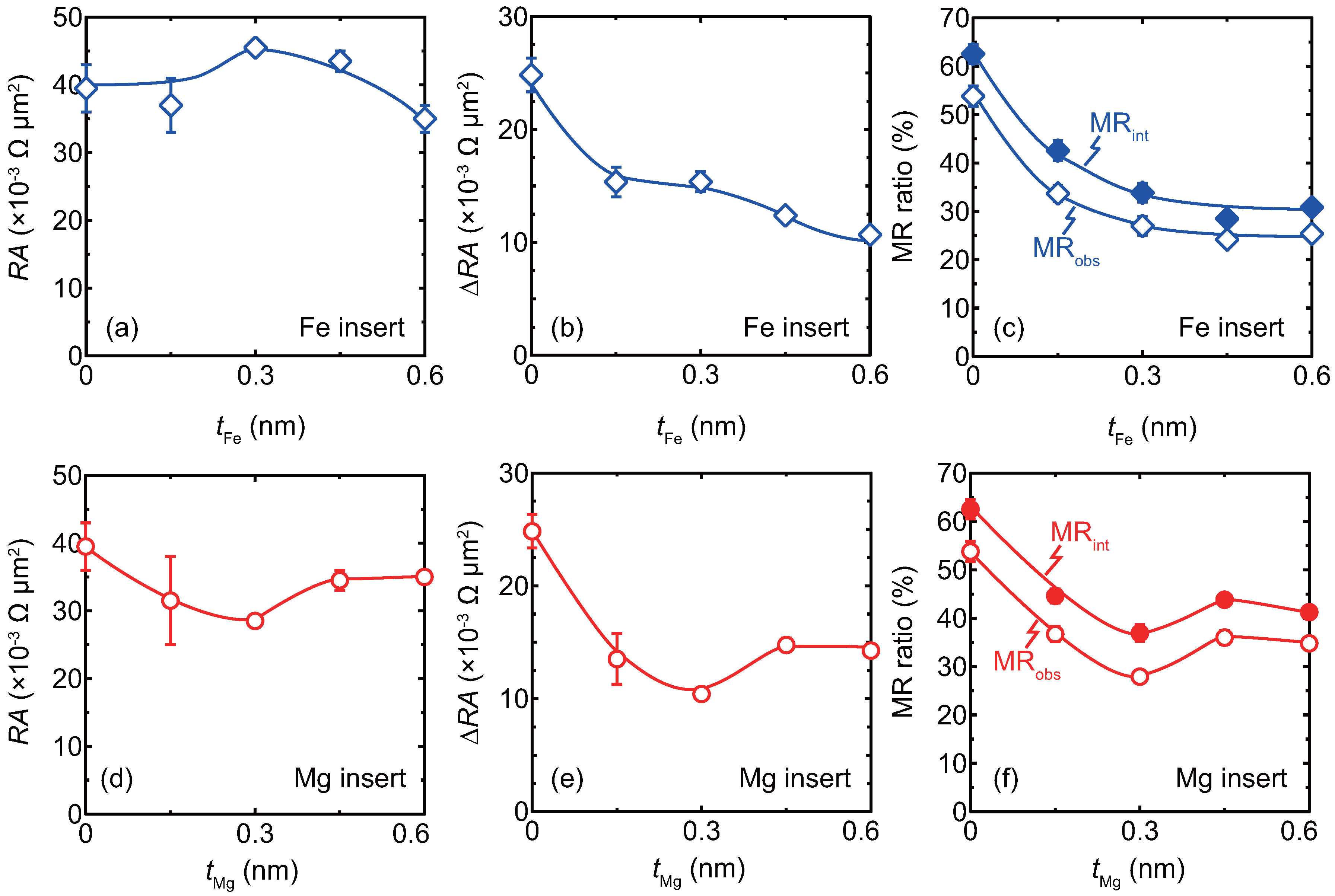
Figure 4.
Bias current density, J dependence of MR curves. Junctions with (a–c) no insert; (d–f) Fe inserts, and (g–i) Mg inserts. The thickness of the inserts is 0.45 nm.
Figure 4.
Bias current density, J dependence of MR curves. Junctions with (a–c) no insert; (d–f) Fe inserts, and (g–i) Mg inserts. The thickness of the inserts is 0.45 nm.

Figure 5.
Bias current density, J, dependence of the output voltage, for the junctions with (a) no insert; (b) Fe inserts, and (c) Mg inserts. The thickness of the inserts is 0.45 nm for (b,c).
Figure 5.
Bias current density, J, dependence of the output voltage, for the junctions with (a) no insert; (b) Fe inserts, and (c) Mg inserts. The thickness of the inserts is 0.45 nm for (b,c).

Figure 6.
Summaries of (a,c) the maximum output voltage, , and (b,d) the critical current density as a function of the insert thickness. (a,b) Fe insert, (c,d) Mg insert.
Figure 6.
Summaries of (a,c) the maximum output voltage, , and (b,d) the critical current density as a function of the insert thickness. (a,b) Fe insert, (c,d) Mg insert.
© 2018 by the authors. Licensee MDPI, Basel, Switzerland. This article is an open access article distributed under the terms and conditions of the Creative Commons Attribution (CC BY) license (http://creativecommons.org/licenses/by/4.0/).
Share and Cite
MDPI and ACS Style
Kubota, T.; Ina, Y.; Wen, Z.; Takanashi, K. Interface Tailoring Effect for Heusler Based CPP-GMR with an L12-Type Ag3Mg Spacer. Materials 2018, 11, 219. https://doi.org/10.3390/ma11020219
AMA Style
Kubota T, Ina Y, Wen Z, Takanashi K. Interface Tailoring Effect for Heusler Based CPP-GMR with an L12-Type Ag3Mg Spacer. Materials. 2018; 11(2):219. https://doi.org/10.3390/ma11020219
Chicago/Turabian StyleKubota, Takahide, Yusuke Ina, Zhenchao Wen, and Koki Takanashi. 2018. "Interface Tailoring Effect for Heusler Based CPP-GMR with an L12-Type Ag3Mg Spacer" Materials 11, no. 2: 219. https://doi.org/10.3390/ma11020219
Note that from the first issue of 2016, this journal uses article numbers instead of page numbers. See further details here.