Effect of Growth Temperature on the Structural and Electrical Properties of ZrO2 Films Fabricated by Atomic Layer Deposition Using a CpZr[N(CH3)2]3/C7H8 Cocktail Precursor

 , ,
, ,
Abstract
:1. Introduction
2. Materials and Methods
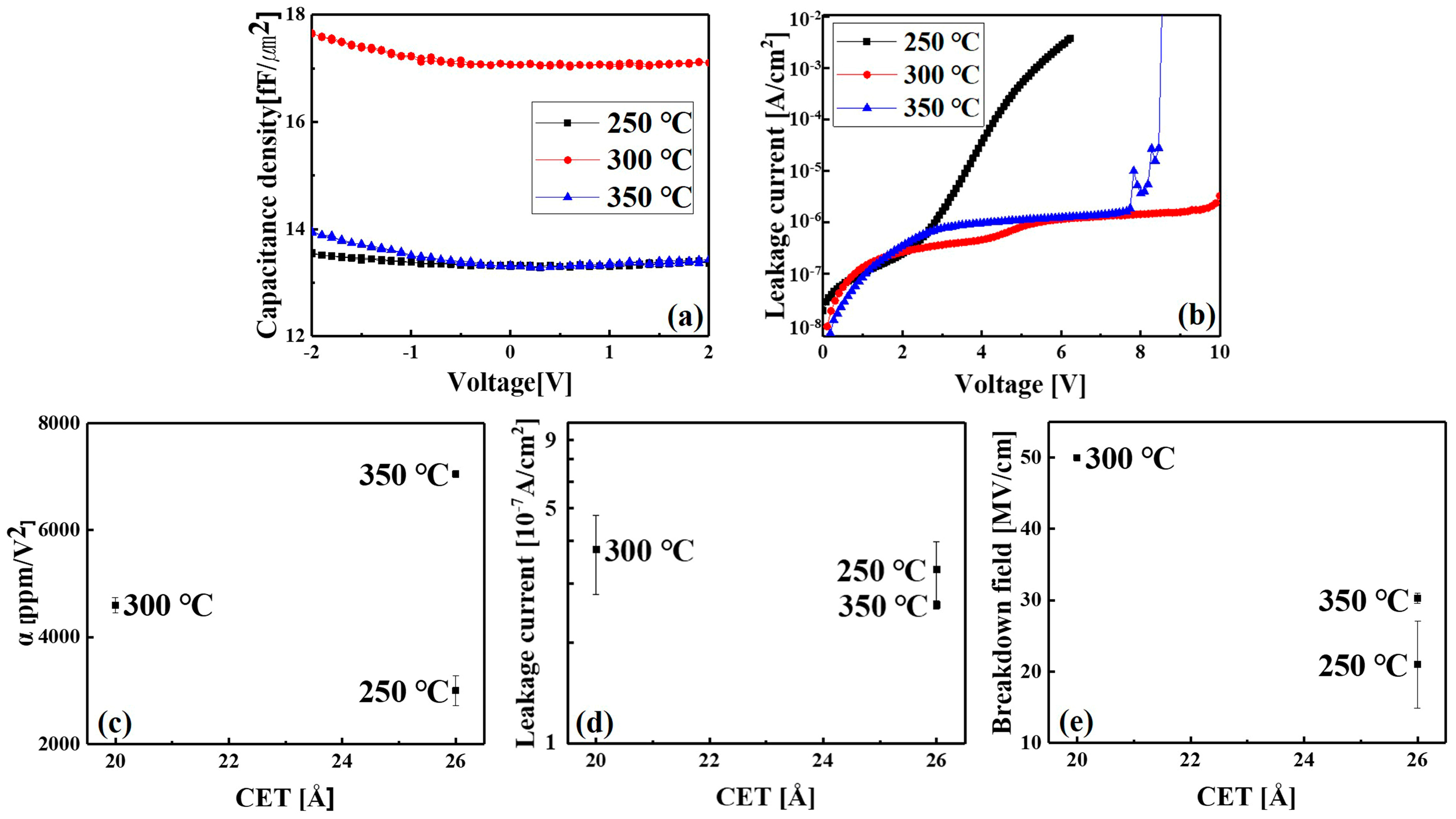
3. Results and Discussion
4. Conclusions
Acknowledgments
Author Contributions
Conflicts of Interest
References
- Panda, D.; Tseng, T.-Y. Growth, dielectric properties, and memory device applications of ZrO2 thin films. Thin Solid Films 2013, 531, 1–20. [Google Scholar] [CrossRef]
- Pešić, M.; Knebel, S.; Geyer, M.; Schmelzer, S.; Böttger, U.; Kolomiiets, N.; Afanas’ev, V.V.; Cho, K.; Jung, C.; Chang, J.; et al. Low leakage ZrO2 based capacitors for sub 20 nm dynamic random access memory technology nodes. J. Appl. Phys. 2016, 119, 064101. [Google Scholar]
- An, J.-K.; Kim, J.-T.; Kang, G.; Oh, N.K.; Hahm, S.-H.; Lee, G.; Park, I.-S.; Yun, J.-Y. ZrO2 film prepared by atomic layer deposition using less viscous cocktail CpZr[n(CH3)2]3/C7H8 precursor and ozone. J. Alloy Compd. 2017, 701, 310–315. [Google Scholar] [CrossRef]
- Lutzer, B.; Simsek, S.; Zimmermann, C.; Stoeger-Pollach, M.; Bethge, O.; Bertagnolli, E. Linearity optimization of atomic layer deposited ZrO2 metal-insulator-metal capacitors by inserting interfacial Zr-doped chromia layers. J. Appl. Phys. 2016, 119, 125304. [Google Scholar] [CrossRef]
- Akinaga, H.; Shima, H. Resistive random access memory (ReRAM) based on metal oxides. Proc. IEEE 2010, 98, 2237–2251. [Google Scholar] [CrossRef]
- Zhao, X.; Vanderbilt, D. Phonons and lattice dielectric properties of zirconia. Phys. Rev. B 2002, 65, 075105. [Google Scholar] [CrossRef]
- Clark, R.D. Emerging applications for high K materials in VLSI technology. Materials 2014, 7, 2913–2944. [Google Scholar] [CrossRef] [PubMed]
- Alimardani, N.; King, S.W.; French, B.L.; Tan, C.; Lampert, B.P.; Conley, J.F., Jr. Investigation of the impact of insulator material on the performance of dissimilar electrode metal-insulator-metal diodes. J. Appl. Phys. 2014, 116, 024508. [Google Scholar] [CrossRef]
- French, R.H.; Glass, S.J.; Ohuchi, F.S.; Xu, Y.-N.; Ching, W.Y. Experimental and theoretical determination of the electronic structure and optical properties of three phases of ZrO2. Phys. Rev. B 1994, 49, 5133–5141. [Google Scholar] [CrossRef]
- Lamperti, A.; Lamagna, L.; Congedo, G.; Spiga, S. Cubic/tetragonal phase stabilization in high-κ ZrO2 thin films grown using O3-based atomic layer deposition. J. Electrochem. Soc. 2011, 158, G221–G226. [Google Scholar] [CrossRef]
- Boscherini, F.; D’Acapito, F.; Galata, S.F.; Tsoutsou, D.; Dimoulas, A. Atomic scale mechanism for the Ge-induced stabilization of the tetragonal, very high-κ, phase of ZrO2. Appl. Phys. Lett. 2011, 99, 121909. [Google Scholar] [CrossRef]
- Lamperti, A.; Cianci, E.; Ciprian, R.; Sangalli, D.; Debernardi, A. Stabilization of tetragonal/cubic phase in Fe doped zirconia grown by atomic layer deposition. Thin Solid Films 2013, 533, 83–87. [Google Scholar] [CrossRef]
- Oh, N.K.; Kim, J.-T.; Kang, G.; An, J.-K.; Nam, M.; Kim, S.Y.; Park, I.-S.; Yun, J.-Y. Oxidant effect of La(NO3)3·6H2O solution on the crystalline characteristics of nanocrystalline ZrO2 films grown by atomic layer deposition. Appl. Surf. Sci. 2017, 394, 231–239. [Google Scholar] [CrossRef]
- Lee, S.B.; Park, I.-S.; Kim, Y.-M.; Yoo, S.J.; Kim, J.-G.; Han, H.N.; Lee, D.N. Elastic softening of sapphire by Si diffusion for dislocation-free GaN. Acta Mater. 2014, 66, 97–104. [Google Scholar] [CrossRef]
- Park, I.-S.; Jung, Y.C.; Seong, S.; Ahn, J.; Kang, J.; Noh, W.; Lansalot-Matras, C. Atomic layer deposition of Y2O3 films using heteroleptic liquid (iPrCp)2Y(iPr-amd) precursor. J. Mater. Chem. C 2014, 2, 9240–9247. [Google Scholar] [CrossRef]
- Kim, K.-R.; Park, I.-S.; Hong, J.P.; Lee, S.S.; Choi, B.L.; Ahn, J. Resistive switching characteristics of HfO2 grown by atomic layer deposition. J. Korean Phys. Soc. 2006, 49, S548–S551. [Google Scholar]
- Park, I.-S.; Lee, T.; Choi, D.-K.; Ahn, J. Metal precursor effects on deposition and interfacial characteristics of HfO2 dielectrics grown by atomic layer deposition. J. Korean Phys. Soc. 2006, 49, S544–S547. [Google Scholar]
- Barreca, D.; Battiston, G.A.; Gerbasi, R.; Tondello, E.; Zanella, P. Zirconium dioxide thin films characterized by XPS. Surf. Sci. Spectra 2000, 7, 303. [Google Scholar] [CrossRef]
- Lung, C.Y.K.; Kukk, E.; Hägerth, T.; Matinlinna, J.P. Surface modification of silica-coated zirconia by chemical treatments. Appl. Surf. Sci. 2010, 257, 1228–1235. [Google Scholar] [CrossRef] [Green Version]
- Gevorgyan, V.; Reymers, A.; Arzakantsyan, M.; Lee, K.; Ahn, J.; Park, I.-S. Influence of annealing temperature on structural and optical properties of undoped and Al-doped nano-ZnO films prepared by sol-gel method. Sci. Adv. Mater. 2016, 8, 878–883. [Google Scholar] [CrossRef]
- Niinisto, J.; Kukli, K.; Kariniemi, M.; Ritala, M.; Leskela, M.; Blasco, N.; Pinchart, A.; Lachaud, C.; Laaroussi, N.; Wang, Z.Y.; et al. Novel mixed alkylamido-cyclopentadienyl precursors for ALD of ZrO2 thin films. J. Mater. Chem. 2008, 18, 5243–5247. [Google Scholar] [CrossRef]
- Aarik, L.; Alles, H.; Aidla, A.; Kahro, T.; Kukli, K.; Niinistö, J.; Mändar, H.; Tamm, A.; Rammula, R.; Sammelselg, V.; et al. Influence of process parameters on atomic layer deposition of ZrO2 thin films from CpZr(NMe2)3 and H2O. Thin Solid Films 2014, 565, 37–44. [Google Scholar] [CrossRef]
- Park, I.-S.; Ryu, K.-M.; Jeong, J.; Ahn, J. Dielectric stacking effect of Al2O3 and HfO2 in metal-insulator-metal capacitor. IEEE Electr. Dev. Lett. 2013, 34, 120–122. [Google Scholar] [CrossRef]


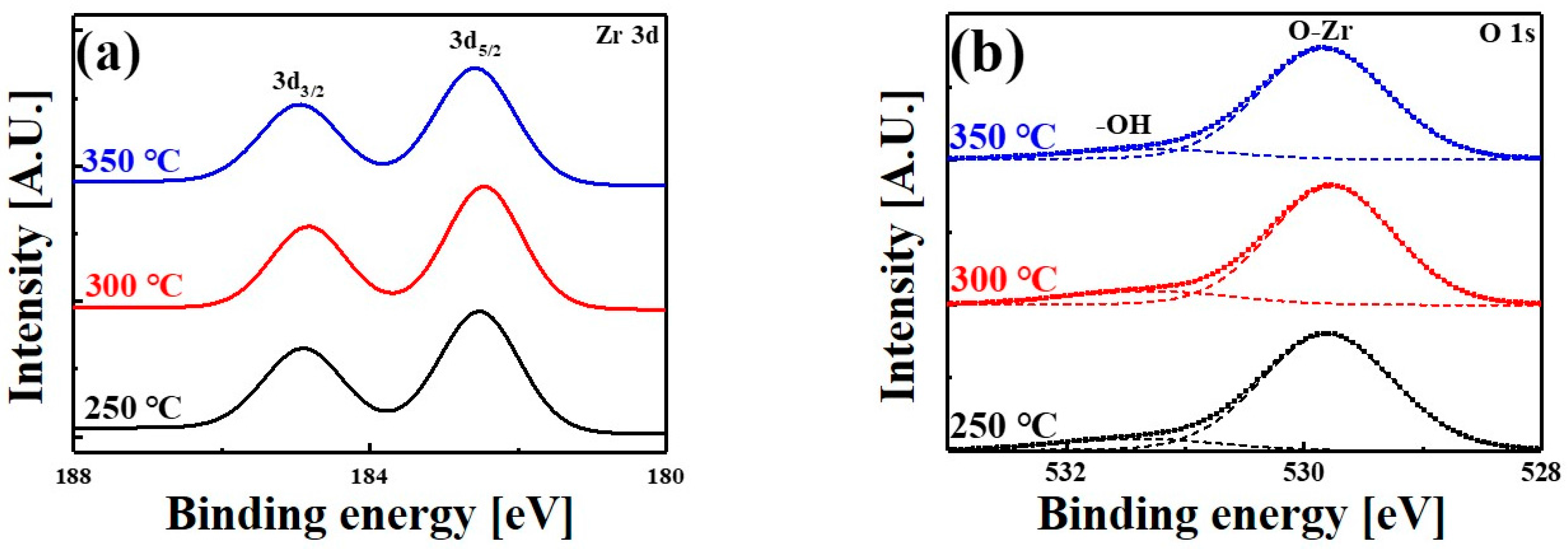
| Temperature (°C) | 3d5/2 (eV) | 3d3/2 (eV) | SOS (eV) |
|---|---|---|---|
| 250 | 182.51 | 184.89 | 2.38 |
| 300 | 182.46 | 184.83 | 2.37 |
| 350 | 182.57 | 184.94 | 2.37 |
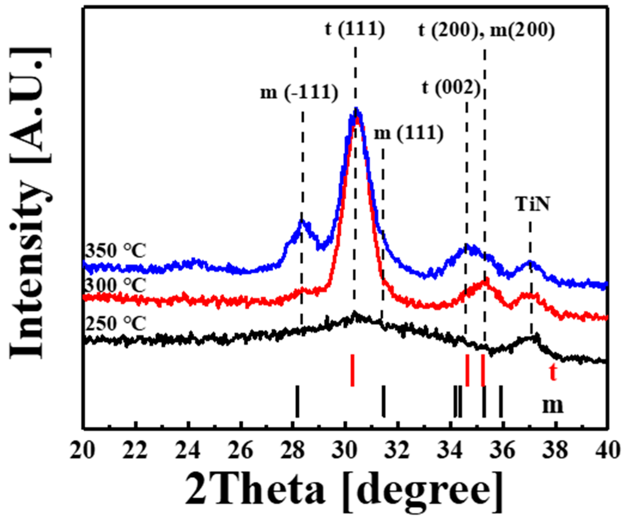
| Temperature (°C) | 28.3° (m) | 30.4° (t) | 31.3° (m) | 34.7° (t) | 35.3° (t, m) |
|---|---|---|---|---|---|
| 25 | - | low | - | - | - |
| 30 | low | high | - | low | medium |
| 35 | medium | high | Low | medium | low |
© 2018 by the authors. Licensee MDPI, Basel, Switzerland. This article is an open access article distributed under the terms and conditions of the Creative Commons Attribution (CC BY) license (http://creativecommons.org/licenses/by/4.0/).
Share and Cite
An, J.-K.; Chung, N.-K.; Kim, J.-T.; Hahm, S.-H.; Lee, G.; Lee, S.B.; Lee, T.; Park, I.-S.; Yun, J.-Y. Effect of Growth Temperature on the Structural and Electrical Properties of ZrO2 Films Fabricated by Atomic Layer Deposition Using a CpZr[N(CH3)2]3/C7H8 Cocktail Precursor. Materials 2018, 11, 386. https://doi.org/10.3390/ma11030386
An J-K, Chung N-K, Kim J-T, Hahm S-H, Lee G, Lee SB, Lee T, Park I-S, Yun J-Y. Effect of Growth Temperature on the Structural and Electrical Properties of ZrO2 Films Fabricated by Atomic Layer Deposition Using a CpZr[N(CH3)2]3/C7H8 Cocktail Precursor. Materials. 2018; 11(3):386. https://doi.org/10.3390/ma11030386
Chicago/Turabian StyleAn, Jong-Ki, Nak-Kwan Chung, Jin-Tae Kim, Sung-Ho Hahm, Geunsu Lee, Sung Bo Lee, Taehoon Lee, In-Sung Park, and Ju-Young Yun. 2018. "Effect of Growth Temperature on the Structural and Electrical Properties of ZrO2 Films Fabricated by Atomic Layer Deposition Using a CpZr[N(CH3)2]3/C7H8 Cocktail Precursor" Materials 11, no. 3: 386. https://doi.org/10.3390/ma11030386