Prior Surface Integrity Assessment of Coated and Uncoated Carbide Inserts Using Atomic Force Microscopy

Abstract
:1. Introduction
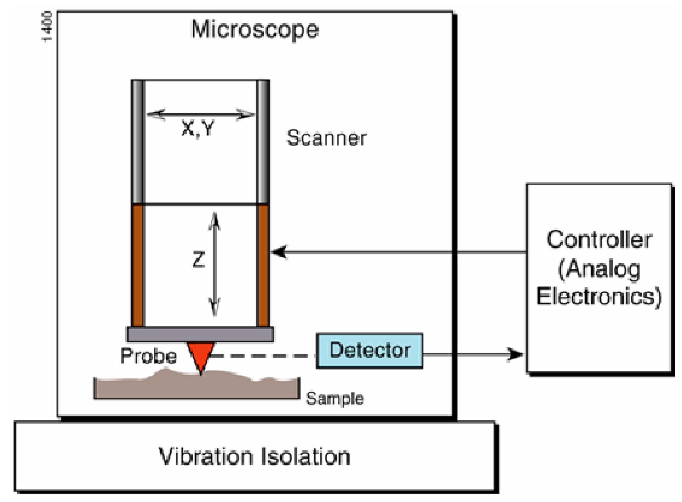
2. Experimental Setup and Hardware Setting


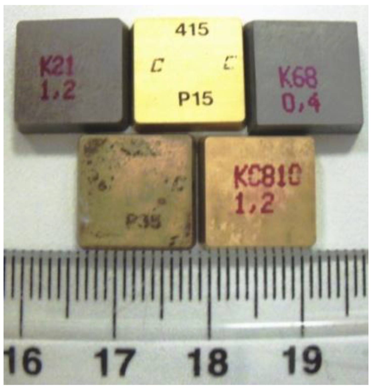
| Insert type | ISO Application Range | Feature | Applications |
|---|---|---|---|
| Kennametal K68 | M10-20 K05-20 (ANSI Range: C3) | low binder content, unalloyed grade WC/Co fine-grained grade | excellent abrasion resistance for machining cast irons, austenitic stainless steels, non-ferrous metals, nonmetals |
| Kennametal K21 | M10-20 K05-20 (ANSI Range: C3) | low binder content, unalloyed grade WC/Co fine-grained grade | excellent abrasion resistance for machining cast irons, austenitic stainless steels, non-ferrous metals, nonmetals |
| Kennametal multicoated KC810 CVD coated carbide | M10-20 K05-20 (ANSI Range: C3) | 1 μm TiN–3 μm Al2O3—5 μm TiC | general steel machining at low to moderate speeds |
| Sandvik CVD multicoated GC415 | (P05-30, K05-20, C6-8) | 1 μm TiN–3 μm Al2O3—5 μm TiC | turning steel and cast iron |
| Sandvik CVD multicoated GC435 | ISO P35 range | 1 μm TiN–3 μm Al2O3—5 μm TiC | steel cutting with decreasing rates of plastic deformation and growth of thermal and mechanical fatigue cracks |
3. Results and Discussion
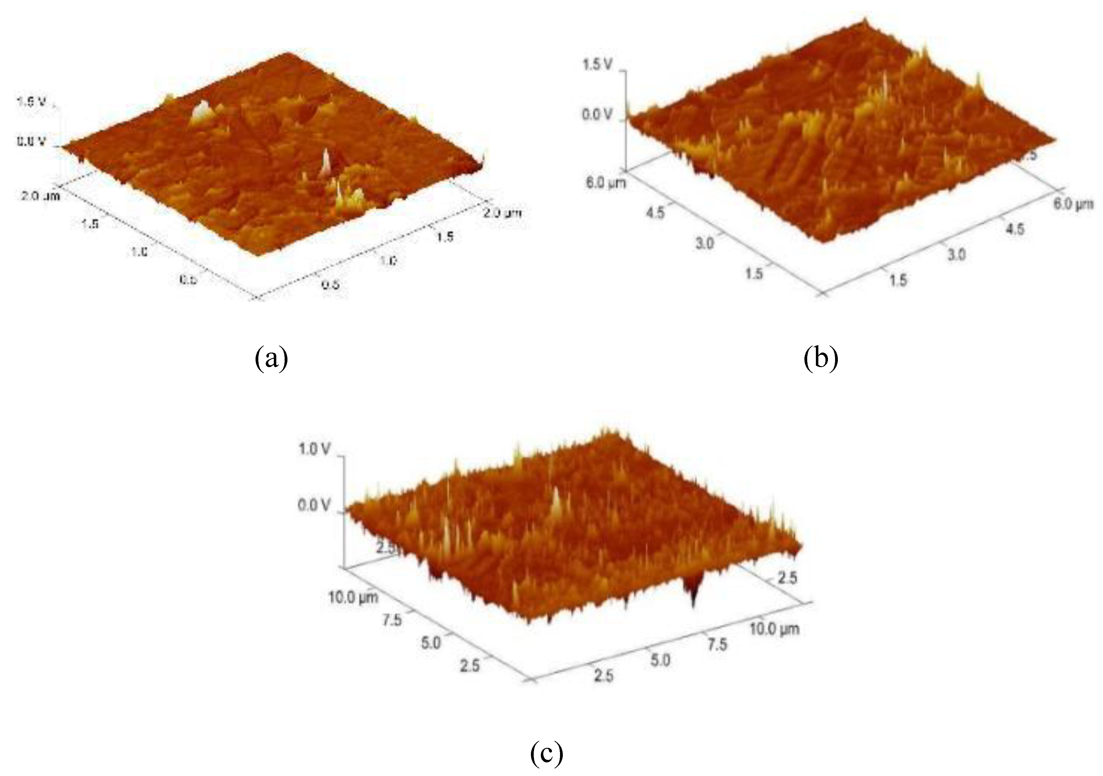
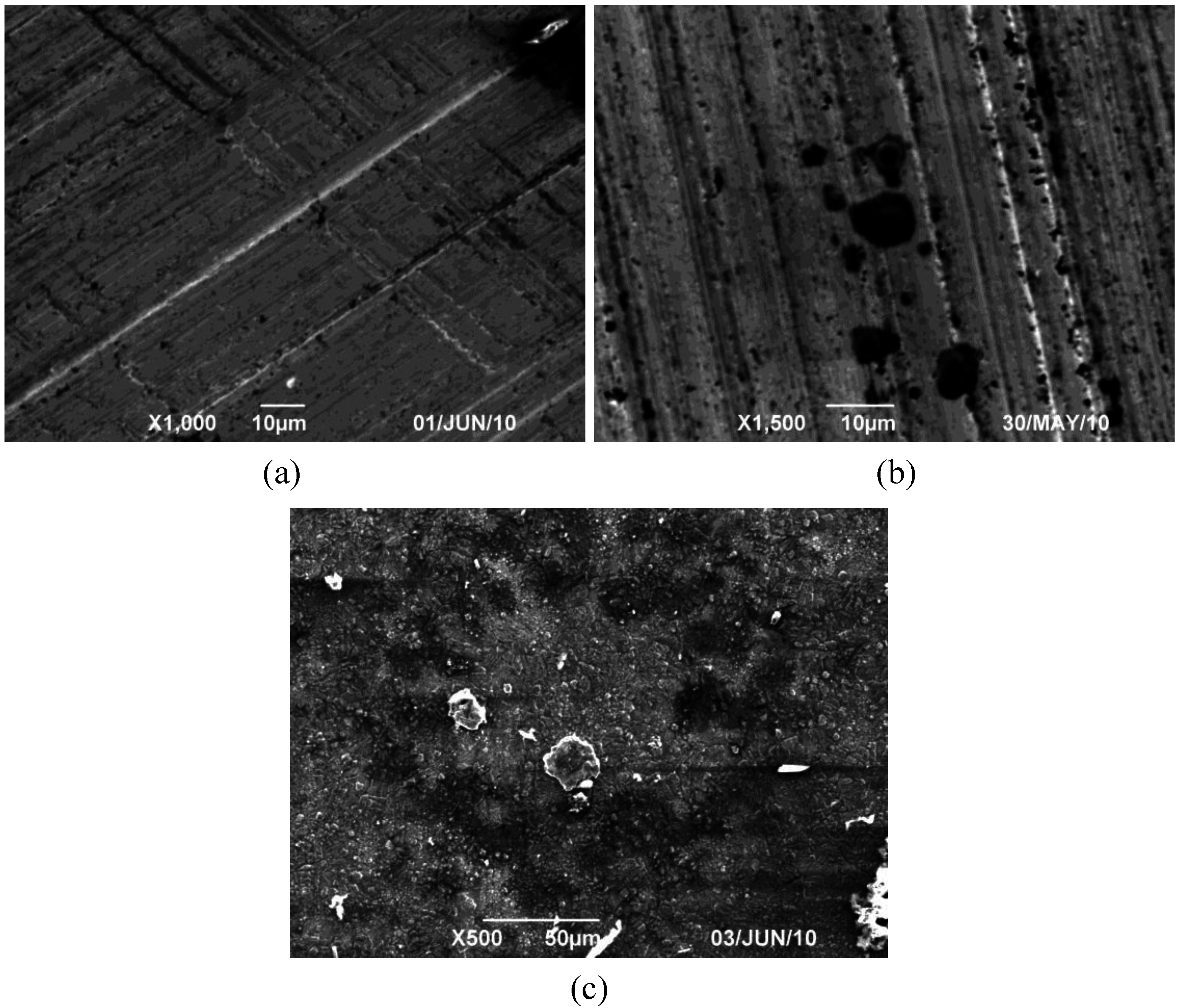
3.1. Selection of Data Types (Captured Image)

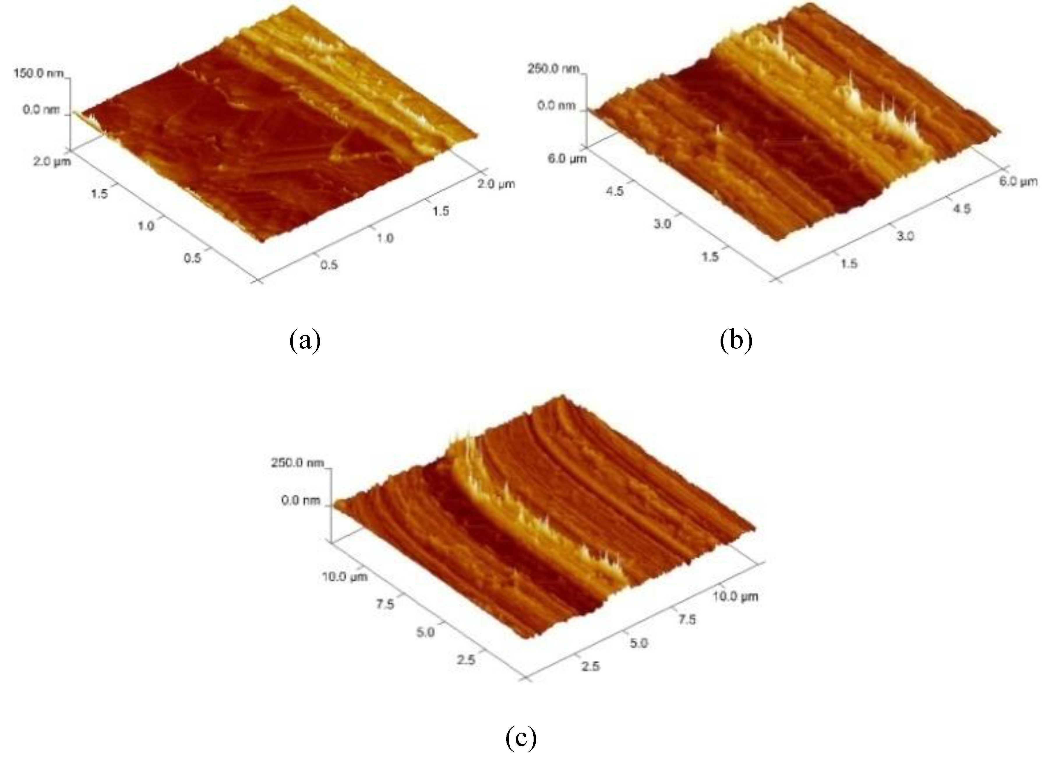
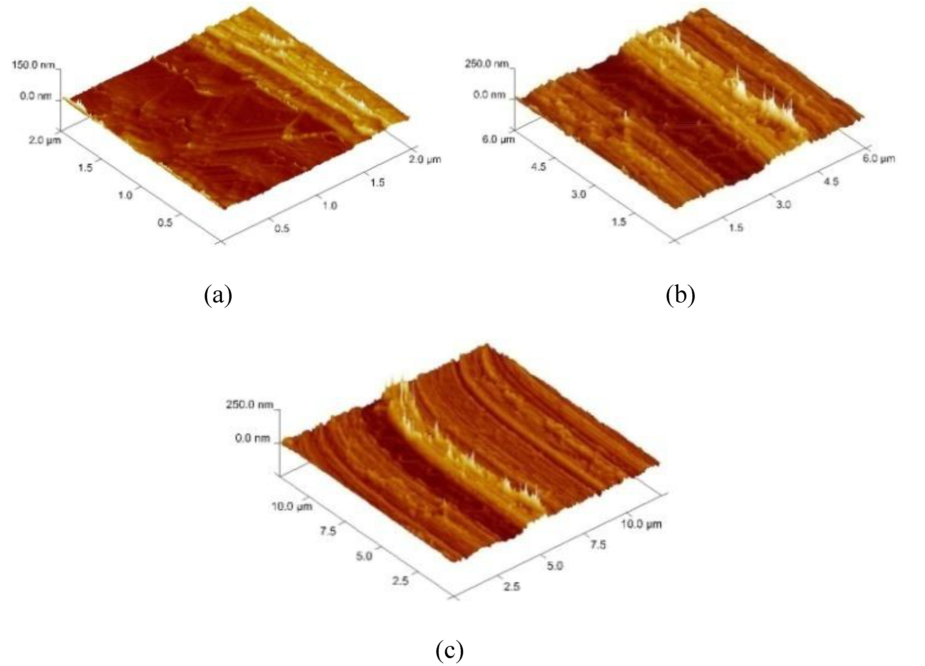
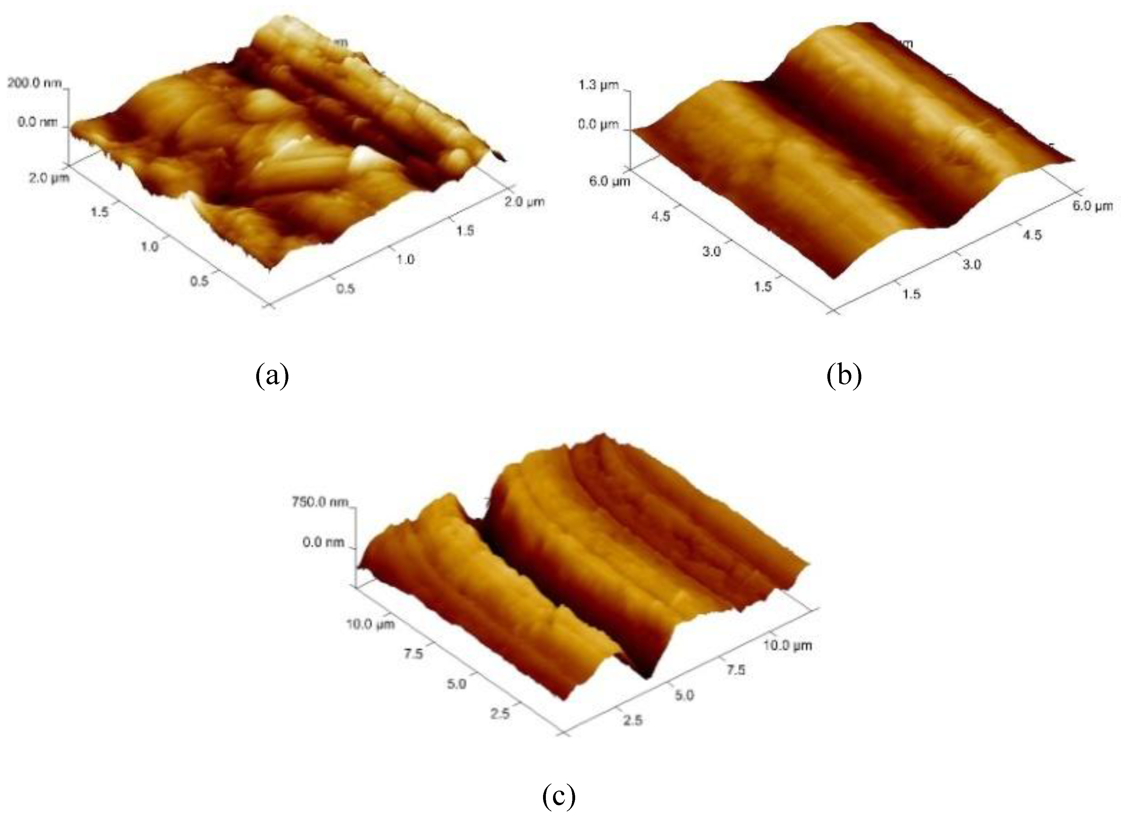
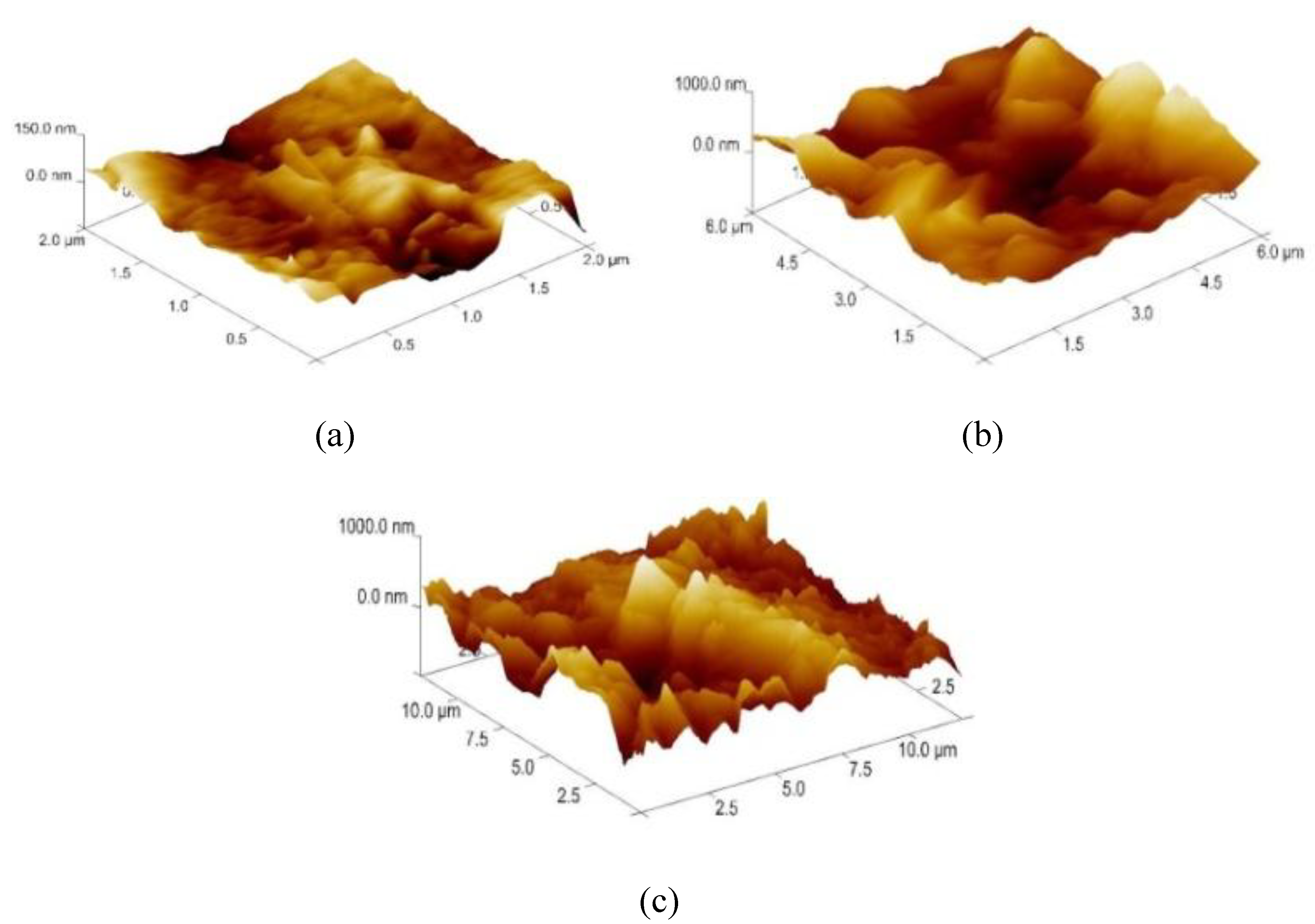
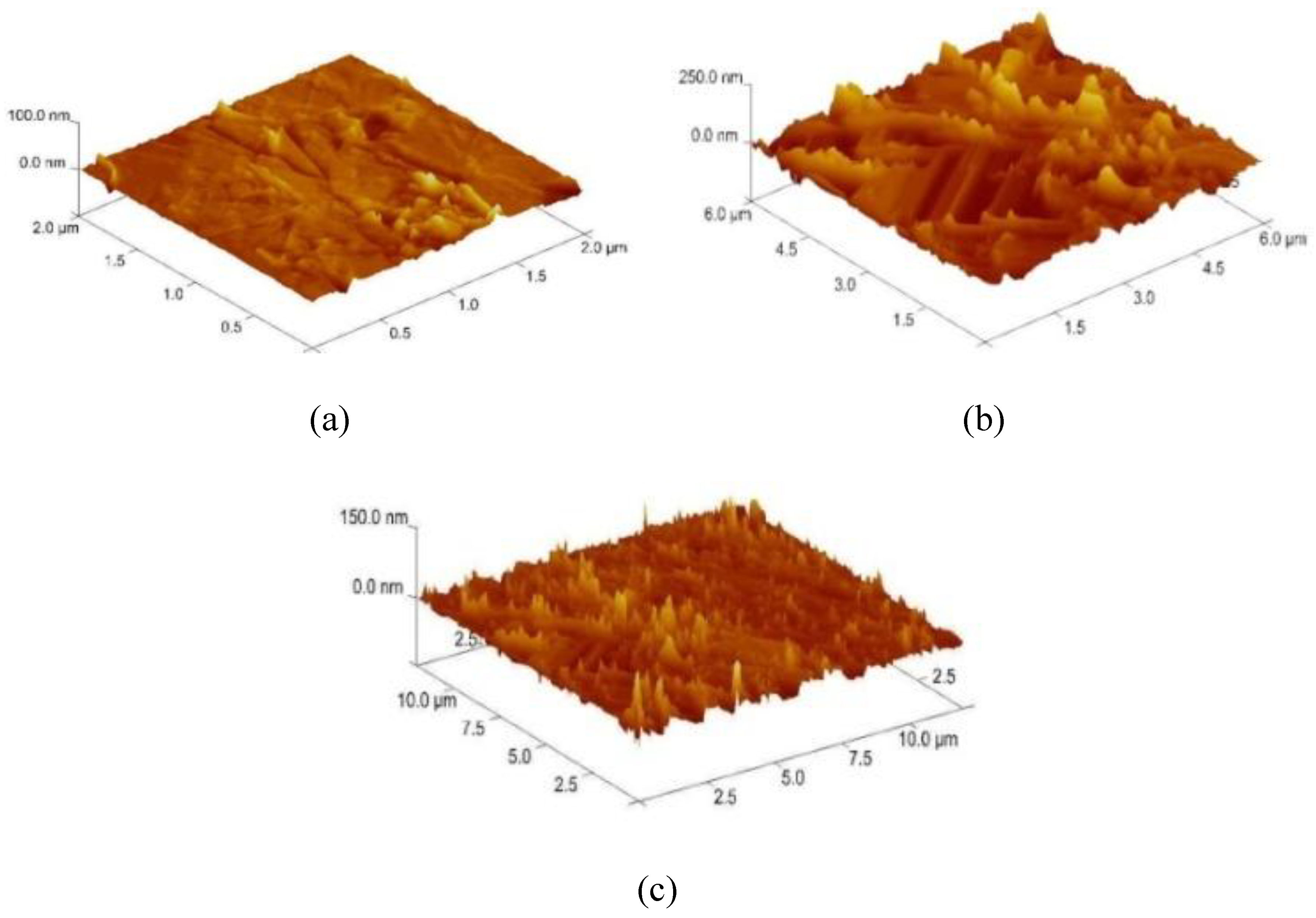
3.2. Determination of the Appropriate Scan Size


3.3. Data Analysis Techniques
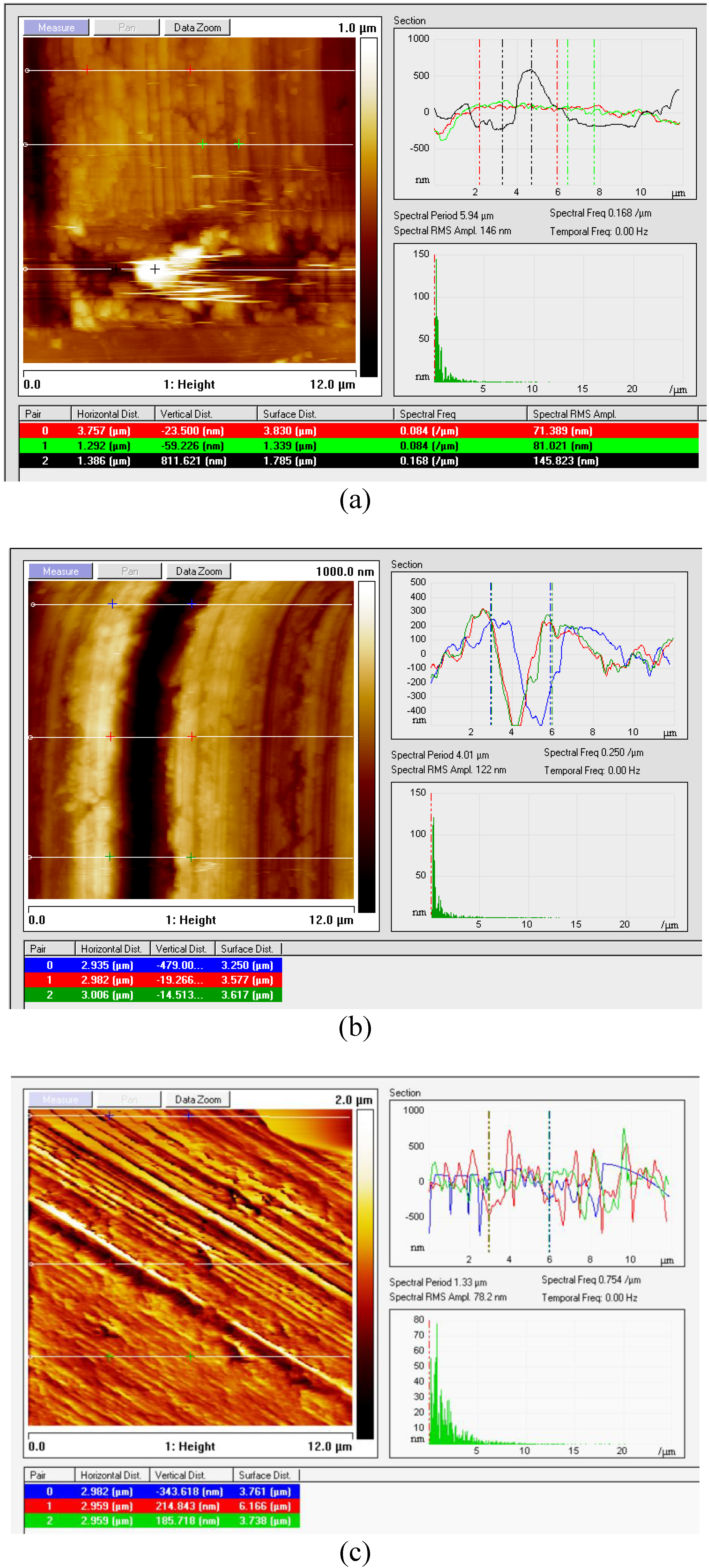
3.3.1. “Roughness” Analysis Parameter of Surface Topography
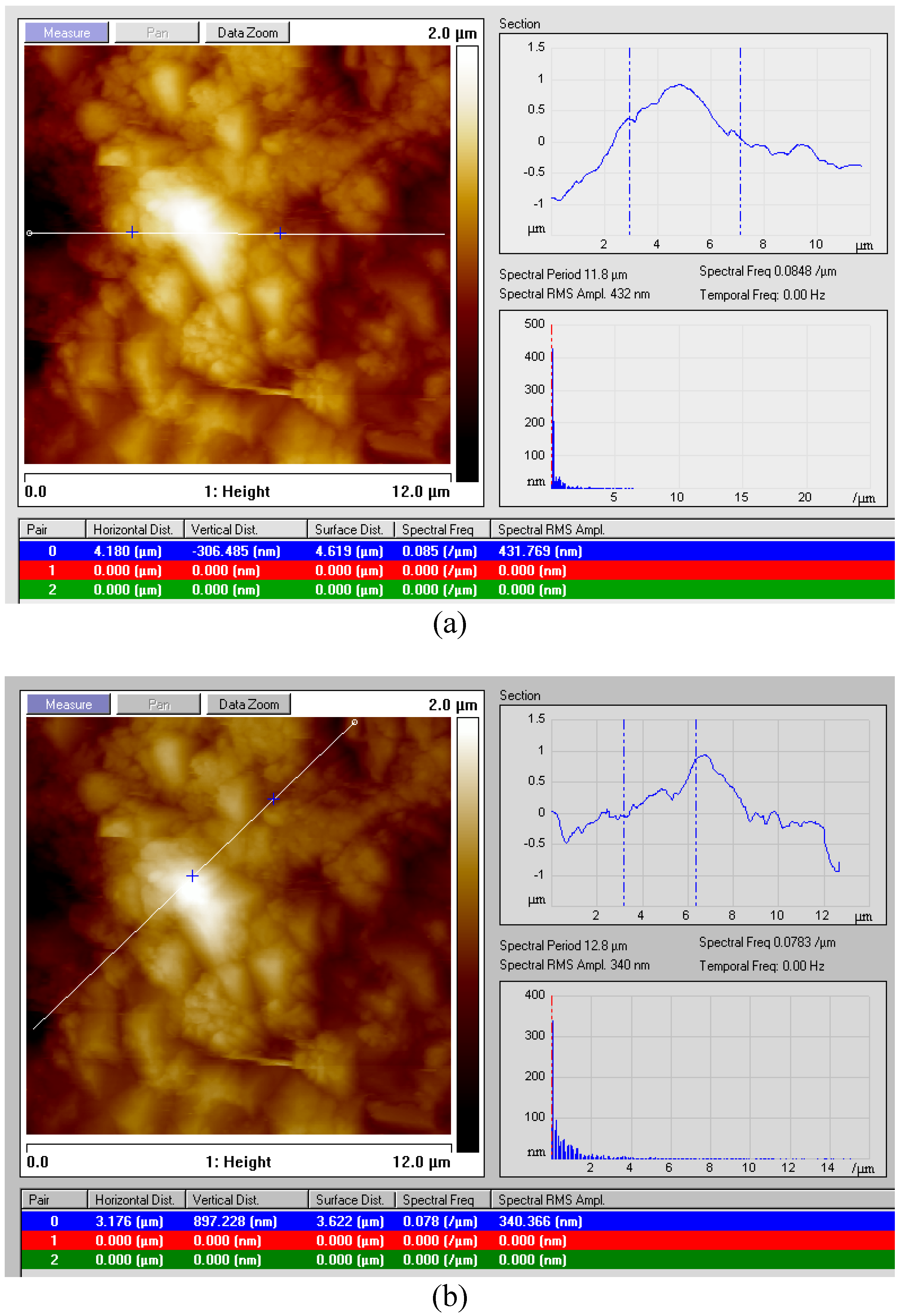
3.3.2. “Section” Analysis of Surface Topography
| Sample No. | Roughness data | Section Data | Notes & Remarks | ||||
|---|---|---|---|---|---|---|---|
| Zrange (nm) | Area Diff.% | Rq (nm) | Ra (nm) | Spectral RMS (nm) | Height Range (nm) | ||
| Sample 1-K68 | 1,281 | 36.1 | 119 | 83.9 | 146 | −250 To 600 |  |
| Sample 2-K68 | 1,114 | 11.1 | 192 | 144 | 12 | −500 To 310 |  |
| Sample 3-K68 | 634 | 9.24 | 84.3 | 65.8 | 101 | −300 To 200 |  |
| Sample 4 = K68 (defect) | 2,855 | 222 | 217 | 161 | 782 | −750 To 750 |  |
| Sample 5 = K21 | 674 | 8.3 | 54.2 | 35.8 | 52.9 | −140 To 215 |  |
| Sample 6-K21 (Defect) | 1,951 | 16.7 | 398 | 341 | 449 | −1,000 To 700 |  |
| Sample No. | Roughness data | Section Data | Notes & Remarks | ||||
|---|---|---|---|---|---|---|---|
| Zrange (nm) | Area Diff. % | Rq (nm) | Ra (nm) | Spectral RMS (nm) | Height Range (nm) | ||
| Sample 1 | 1,224 | 22.3 | 186 | 112 | 208 | −500 To 485 |  |
| Sample 2 | 1,954 | 21.4 | 291 | 227 | 432 | ±1,000 |  |
| Sample 3 | 1,355 | 12.4 | 168 | 130 | 86.7 | −350 To 390 |  |
| Sample 4 | 1,148 | 18.3 | 164 | 128 | 146 | −450 To 490 |  |
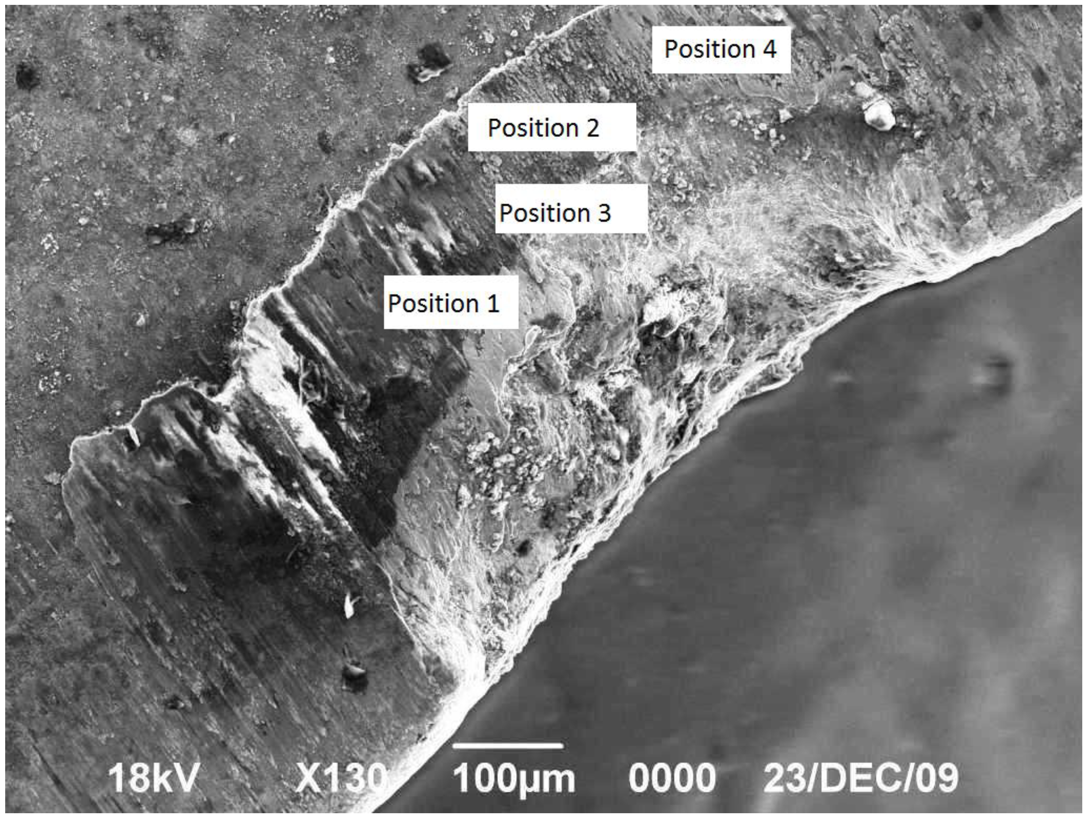
| Sample 5 (worn-Pos. 1, Figure 1) | 612 | 5.84 | 90.2 | 73.4 | 78.9 | −160 To 200 |  |
| Sample 5 (worn-Pos. 2, Figure 1) | 2,912 | 107 | 500 | 398 | 818 | −800 To 2,000 |  |
| Sample 5 (worn-Pos. 3, Figure 1) | 2,462 | 31.1 | 311 | 236 | 815 | 0 To 2,000 |  |
| Sample 5 (worn-Pos. 4, Figure 1) | 978 | 8.09 | 123 | 97.4 | 160 | ±250 |  |

3.4. A Recommended Strategy for Prior Surface Integrity Assessment
| Seq. | Type of surface Imperfections | Roughness data | Section Data | Hardware and Software Setting | ||||
|---|---|---|---|---|---|---|---|---|
| Zrange (nm) | Area Diff. % | Rq (nm) | Ra (nm) | Sp. RMS (nm) | Height Range (nm) | |||
| 1 | Preliminary surface examination | • | • | • | a) Use at least three different samples. b) Use maximum available scan size. c) Use “Height” image. | |||
| 2 | Normal defects free surface | • | • | • | • | |||
| 3 | Regular widespread roughness pattern | • | • | • | • | |||
| 4 | Tiny localized surface defects | • | • | • | a) Compare with normal reference topography (Proced. 2). | |||
| 5 | Manufacturing coating imperfections | • | • | |||||
| 6 | Worn edge | • | • | a) Further SEM or/and OM is preffered. | ||||
4. Conclusions
Acknowledgements
References
- Oraby, S.; Alaskari, A. On the variability of tool wear and life at disparate operating parameters. Kuwait J. Sci. Eng. 2008, 1B, 123–150. [Google Scholar]
- Oraby, S.; Almeshaiei, E.; Alaskari, A. An adaptive control simulation approach based on a mathematical model optimization algorithm for rough turning. Kuwait J. Sci. Eng. 2003, 30, 213–234. [Google Scholar]
- Davim, J.P.; Mata, F. Chemical vapour deposition (CVD) diamond coated tools performance in machining of PEEK composites. Mater. Design 2008, 29, 1568–1574. [Google Scholar] [CrossRef]
- Mallika, K.; Komanduri, R. Diamond coatings on cemented tungsten carbide tools by low-pressure microwave. Wear 1999, 224, 245–266. [Google Scholar] [CrossRef]
- Bouzakis, K.-D.; Michailidis, N.; Vidakis, N.; Efstathiou, K. Failure mechanisms of physically vapour deposited coated hardmetal cutting inserts in turning. Wear 2001, 248, 29–37. [Google Scholar] [CrossRef]
- Kodama, M.; Bunshah, R.F. Interrupted cutting tests of cemented carbide tools coated by physical vapor deposition and chemical vapor deposition techniques. Thin Solid Films 1982, 96, 53–58. [Google Scholar] [CrossRef]
- Kِnig, U.; Tabersky, R.; Van den Berg, H. Research, Development and performance of cemented carbide tools coated by plasma-activated chemical vapour deposition. Surf. Coat. Tech. 1991, 50, 57–62. [Google Scholar] [CrossRef]
- Schmutz, J.E.; Fuchs, H.; Hölscher, H. Measuring wear by combining friction force and dynamic force microscopy. Wear 2010, 268, 526–532. [Google Scholar] [CrossRef]
- Panjan, P.; Kek Merl, D.; Zupanič, F.; Čekada, M.; Panjan, M. SEM study of defects in PVD hard coatings using focused ion beam milling. Surf. Coat. Tech. 2008, 202, 2302–2305. [Google Scholar] [CrossRef]
- Huang, M.D.; Lin, G.Q.; Zhao, Y.H.; Sun, C.; Wen, L.S.; Dong, Ch. Macro-particle reduction mechanism in biased arc ion plating of TiN. Surf. Coat. Tech. 2003, 176, 109–114. [Google Scholar] [CrossRef]
- Srikant-Nekkanty, M.S. Characterization of Damage & Optimization of Thin Film Coatings on Ductile Substrates. Ph.D Thesis, Industrial& Systems Engineering Program, The Ohio State University, Columbus, OH, USA, 2009.
- Alaskari, A.M.; Oraby, S.E.; Almazrouee, A.I. SEM and AFM investigations of surface defects and tool wear of multilayers coated carbide inserts. In Proceedings of the International Conference on Manufacturing Systems Engineering WASET-ICMSE, Dubai, United Arab Emirates, January 2011; pp. 1299–1303.
- Binnig, G.; Quate, C.F. Atomic force microscope. Phys. Rev. Lett. 1986, 56, 930–933. [Google Scholar] [CrossRef] [PubMed]
- AFM Resource Library—Agilnet Technology. Available online: http://www.afmuniversity.org (accessed on 13 December 2010).
- NanoScope Software 6.13 User Guide, V.I.I. Version; Veeco Instruments Inc.: Plainview, NY, USA, 2004.
- Koinkar, V.; Bhushan, B. Effect of scan size and surface roughness on microscale friction measurements. J. Appl. Phys. 1997, 81, 2472. [Google Scholar] [CrossRef]
- Ankudinov, A.V.; Titkov, A.N.; Shubina, T.V.; Ivanov, S.V.; Kop’ev, P.S. Cross-sectional atomic force microscopy of ZnMgSSe- and BeMgZnSe-based laser diodes. Appl. Phys. Lett. 1999, 75, 2626. [Google Scholar] [CrossRef]
- Oraby, S.E.; Hayhurst, D.R. Development of models for tool wear force relationships in metal cutting. Int. J. Mech. Sci. 1991, 33, 125–138. [Google Scholar] [CrossRef]
- Oraby, S.E.; Hayhurst, D.R. Tool life determination based on the measurement of wear and tool force ratio variation. Int. J. Mach. Tools Manuf. 2004, 44, 1261–1269. [Google Scholar] [CrossRef]
© 2011 by the authors; licensee MDPI, Basel, Switzerland. This article is an open access article distributed under the terms and conditions of the Creative Commons Attribution license (http://creativecommons.org/licenses/by/3.0/).
Share and Cite
Oraby, S.; Alaskari, A.; Almazrouee, A. Prior Surface Integrity Assessment of Coated and Uncoated Carbide Inserts Using Atomic Force Microscopy. Materials 2011, 4, 633-650. https://doi.org/10.3390/ma4040633
Oraby S, Alaskari A, Almazrouee A. Prior Surface Integrity Assessment of Coated and Uncoated Carbide Inserts Using Atomic Force Microscopy. Materials. 2011; 4(4):633-650. https://doi.org/10.3390/ma4040633
Chicago/Turabian StyleOraby, Samy, Ayman Alaskari, and Abdulla Almazrouee. 2011. "Prior Surface Integrity Assessment of Coated and Uncoated Carbide Inserts Using Atomic Force Microscopy" Materials 4, no. 4: 633-650. https://doi.org/10.3390/ma4040633