1. Introduction
In a coated conductor architecture, c-axis oriented YBCO films for superconducting applications, must be deposited on flexible,
Rolling
Assisted
Biaxially
Textured (RABiTS) Ni-5%W substrates [
1,
2]. Ceramic buffer layers are deposited in between the substrate and YBCO layer to prevent chemical interactions and diffusion of the metallic substrate into the superconducting YBCO. The high temperature processing of YBCO layers in oxygen atmosphere can cause penetration of the Ni atoms from the substrate into the superconducting layer and oxidation of the Ni-5%W substrate. These adverse interactions need to be prevented by the presence of buffer layers which necessarily not only stop the diffusion but should also transfer the epitaxial texture of the RABiTS Ni-5%W substrate to the superconducting layer. Many buffer layers including CeO
2, YSZ, La
2Zr
2O
7, Gd
2Zr
2O
7 have been prevalently used [
3,
4,
5,
6,
7,
8,
9,
10,
11,
12]. La
2Zr
2O
7 (LZO) is used as one of the prominent buffer layer because of its closed packed pyrochlore structure with a lattice parameter of 10.79 Å. It has a low lattice mismatch to both YBCO and Ni-5%W substrate (0.5% and 1.8% mismatch to YBCO, a- and b-axes, respectively and 7.6% to RABiTS Ni-5%W substrate) [
7]. Many different kinds of deposition techniques can be adopted for the deposition of the buffer layers and the final superconducting layer. Chemical solution deposition (CSD) has proven to be an important and cost-effective method for depositing YBa
2Cu
3O
7−x (YBCO) based second generation superconductors [
13,
14]. Furthermore, CSD is one of the cheapest and easily adaptable methods to suit the needs of the buffer layer deposition under non-vacuum conditions. Many of the CSD methods use methoxyethanol or propionic acid based solvents to prepare good quality solutions and in turn buffer layers of good texture and crystallinity [
4,
5,
8,
9]. However, water based LZO solutions are preferred for environmental and economic reasons.
In our laboratory, LZO precursor solutions using water as main solvent have been prepared and buffer layers based on these solutions were deposited taking into account the study of Caroff
et al. which reported a minimum thickness of 150 nm to ensure a sufficient texture quality and to absorb most of the defects of the substrate [
15]. The effective use of these crack-free and crystalline LZO buffer layers of 40–150 nm thickness from water based solutions in transferring the texture to the superconducting layer was studied by depositing YBCO and measuring their critical current [
9,
10,
16].
Besides extensive crystallinity studies published elsewhere, we here present an XPS study used as an effective tool in optimization of the performance of the LZO layer by studying the in-depth composition of the elements and the inter-diffusion thickness of the Ni substrate and the LZO layer [
17]. These LZO layers were prepared under reducing conditions to prevent oxidation of the Ni-5%W substrate. Technically, the LZO buffer layers annealed under reducing conditions (in Ar-5%H
2 gas) are further processed by depositing YBCO on top of them, under oxidizing conditions. The effective action of the buffer layer is to prevent the oxidation of the Ni-5%W substrate and penetration of Ni into the YBCO layer during the YBCO annealing under oxidizing conditions. There are reports that indicate that nickel oxide (NiO) is formed during the annealing step on the interface of the substrate and LZO layer after deposition of YBCO [
16]. Here, the as-prepared LZO buffer layers from water-based precursors are processed under YBCO processing conditions (in oxygen atmosphere) without depositing YBCO. Their buffer layer action is compared with that of the as-prepared LZO buffer layers prepared under reducing conditions using XPS. Four different LZO layers from different water-based precursors under as-prepared and under YBCO annealing conditions were studied using XPS.
2. Results and Discussion
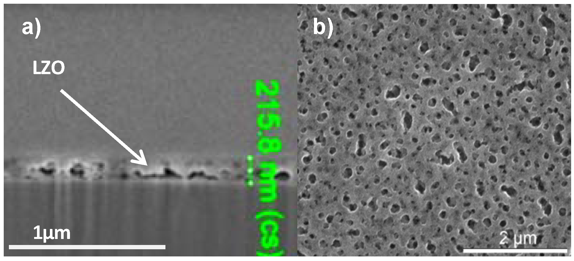
All layers exhibit crack free surfaces, unless stated otherwise, as is shown in
Figure 1a, b for a layer synthesized using system 2. A TEM bright field image of a cross section throughout the LZO layer is shown in
Figure 1b. Bright areas in the LZO layers are allocated to nanovoids [
18]. The sample thickness of the different LZO layers is given in
Table 1. The values for the thickness determined by ellipsometry accord well with the results from TEM measurements.
Figure 1.
(a) Scanning and (b) Transmission Electronic Microscopy images of a thin layer prepared from system 2.
Figure 1.
(a) Scanning and (b) Transmission Electronic Microscopy images of a thin layer prepared from system 2.
Table 1.
Overview of the chemical composition of the precursors used for preparation of the Lanthanum zirconate (LZO) layers.
Table 1.
Overview of the chemical composition of the precursors used for preparation of the Lanthanum zirconate (LZO) layers.
| | Precursor salts | Chelating agent | Additives | Polymer | Thickness |
|---|
| System 1 | La-acetate
Zr-acetate hydroxide | TEA | Acetic Acid, TEA, NH4OH | - | 40 nm a |
| System 2 | La-acetate
Zr-n-propoxide | EDTA | Acetic Acid, EDA, EG NH4OH | - | 110 nm a
100 nm b |
| System 3 | La-acetate
Zr-n-propoxide | EDTA | Acetic Acid, EDA, EG NH4OH | PVP | 220 nm a
205–225 nm b |
| System 4 | La-acetate
Zr-n-propoxide | EDTA | Acetic Acid, AMP, NH4OH | PVP | 125 nm a
150 nm b |
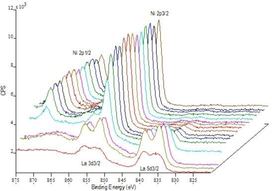
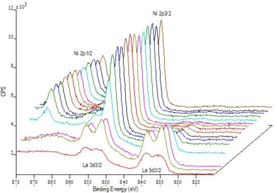
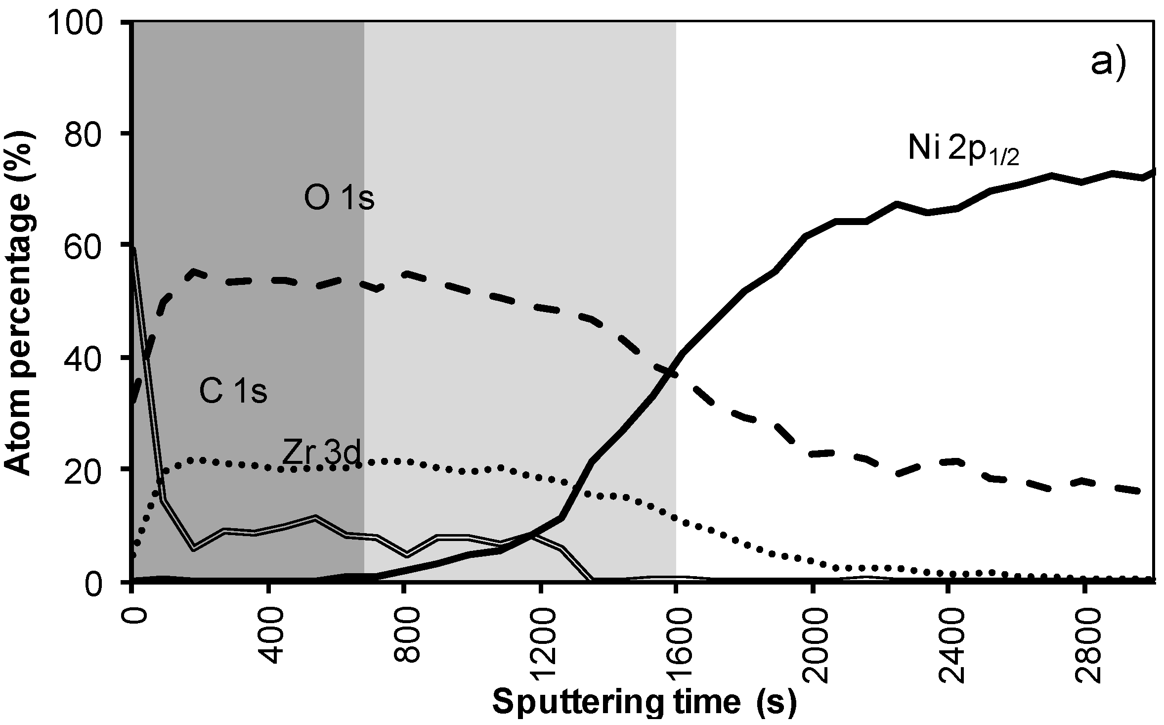
Figure 2a,b shows the results of the XPS depth profiling for samples synthesized using system 1 before and after annealing respectively. From these figures it is observed that on top of the sample mainly carbon is present due to a thin layer of surface contamination. After one sputter cycle the majority of the carbon has been sputtered off and predominantly La, Zr and O peaks are registered. Results from XPS measurements are shown in
Table 2.
The observed stoichiometry of La/Zr in the XPS measurements is not exactly 1:1. The use of standards for the determination of correction factors could compensate for this apparent off stoichiometry [
17]. However there is no physicochemical reason to doubt the constitution of the LZO layers, thus no additional calibrations were performed. Nevertheless for each sample the presence of phase-pure La
2Zr
2O
7 was confirmed with XRD/RHEED analysis.
The thickness of the LZO layer is marked with a (light + dark) grey box on the graphs. The time it takes for the Zr and La concentration to diminish to half of their maximum value was taken as a limit. This approximately coincides with the point where the nickel concentration has increased until half its maximum value. The nickel-free zone is marked with a dark grey box.
The sputter rate of La
2Zr
2O
7 was determined by comparing the thickness of the film measured with TEM or ellipsometry with the time needed to sputter through the La
2Zr
2O
7 layer, more precise the time it takes for the Zr and La concentrations to diminish to half their maximum value. In system 1,
Figure 2a, this takes approximately 250 s, for a 40 nm thick LZO film inferring a sputter rate of 0.16 nm/s. Performed for all samples, the estimated average sputter rate for LZO is 0.17 ± 0.1 nm/s, or 1.13 times faster compared to the sputter rate of Ta
2O
5. This average sputter rate is used in this paper to correlate sputter time to thickness of specific zones.
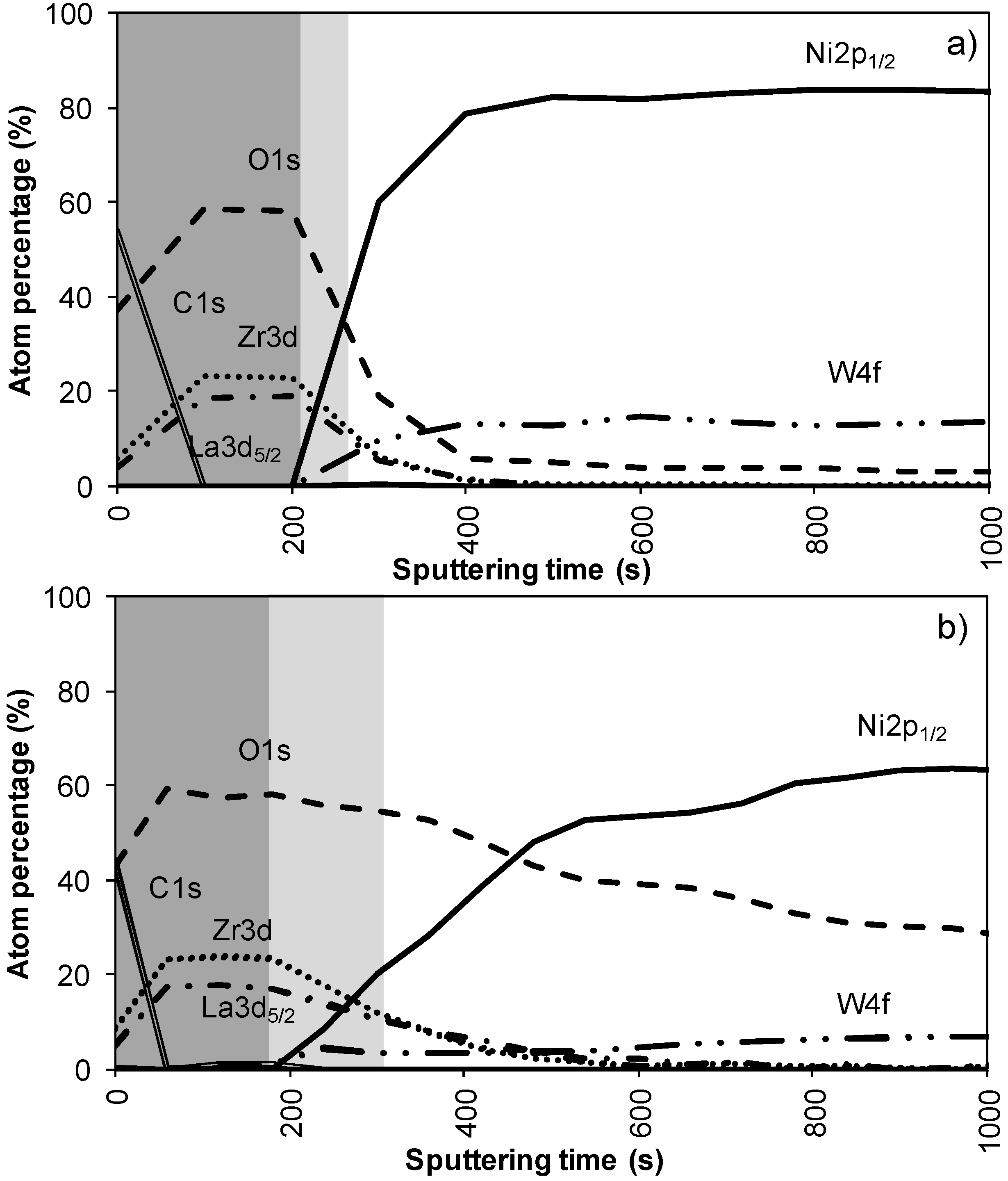
In system 1, Ni 2p1/2 and W 4f peaks were first observed after 300 seconds of sputtering. Based on the sputter rate of La2Zr2O7 it can be concluded that the nickel free region, marked as a dark grey area, on top of the sample is around 34 nm (200 s). After more than 500 s of sputtering the Zr and La peaks disappeared from the spectra.
Annealing this sample, thus mimicking an YBCO deposition, resulted in an increase in diffusion of all elements (
Figure 2b). The steepness of the curves vastly decreases and the region where both Ni/W and La/Zr are present is at least doubled. The thickness of the nickel free zone slightly decreased. Nickel is now observed after 240 s of sputtering, rendering a rather thin nickel free zone at the top of the sample.
Table 2.
Overview of the XPS depth profiling experiments.
Table 2.
Overview of the XPS depth profiling experiments.
| LZO layers | dlayer (elllipso-metry) (nm) | Strong increase in Ni signal after (s sputtering) | Zr signal at Half Max after (s sputtering) | Ni signal Start plateau (s sputtering) | First Ni peak (s sputtering) |
|---|
| System 1 | 40 | 200 | 250 | 400 | 300 |
System 1
YBCO annealed | | 180 | 300 | 550 | 240 |
| System 2 | ~110 | 560 | 660 | 720 | 600 |
System 2
YBCO annealed | | 500 | 630 | 1200 | 550 |
| System 3 | 280 | 810
Start 550 s
Strong increase 1000 | 1600 | 2000 | 720 |
System 3
YBCO annealed | | 540
Start 260 s
Strong increase 700 | 1100 | 1600 | 540 |
| System 4 | 125–150 | 500 | 580 | 900 | 600 |
System 4
YBCO Annealed | | 500 | 670 | 1400 | 550 |
Figure 2.
XPS depth profile of a buffer layered sample using system 1 (a) before and (b) after annealing.
Figure 2.
XPS depth profile of a buffer layered sample using system 1 (a) before and (b) after annealing.
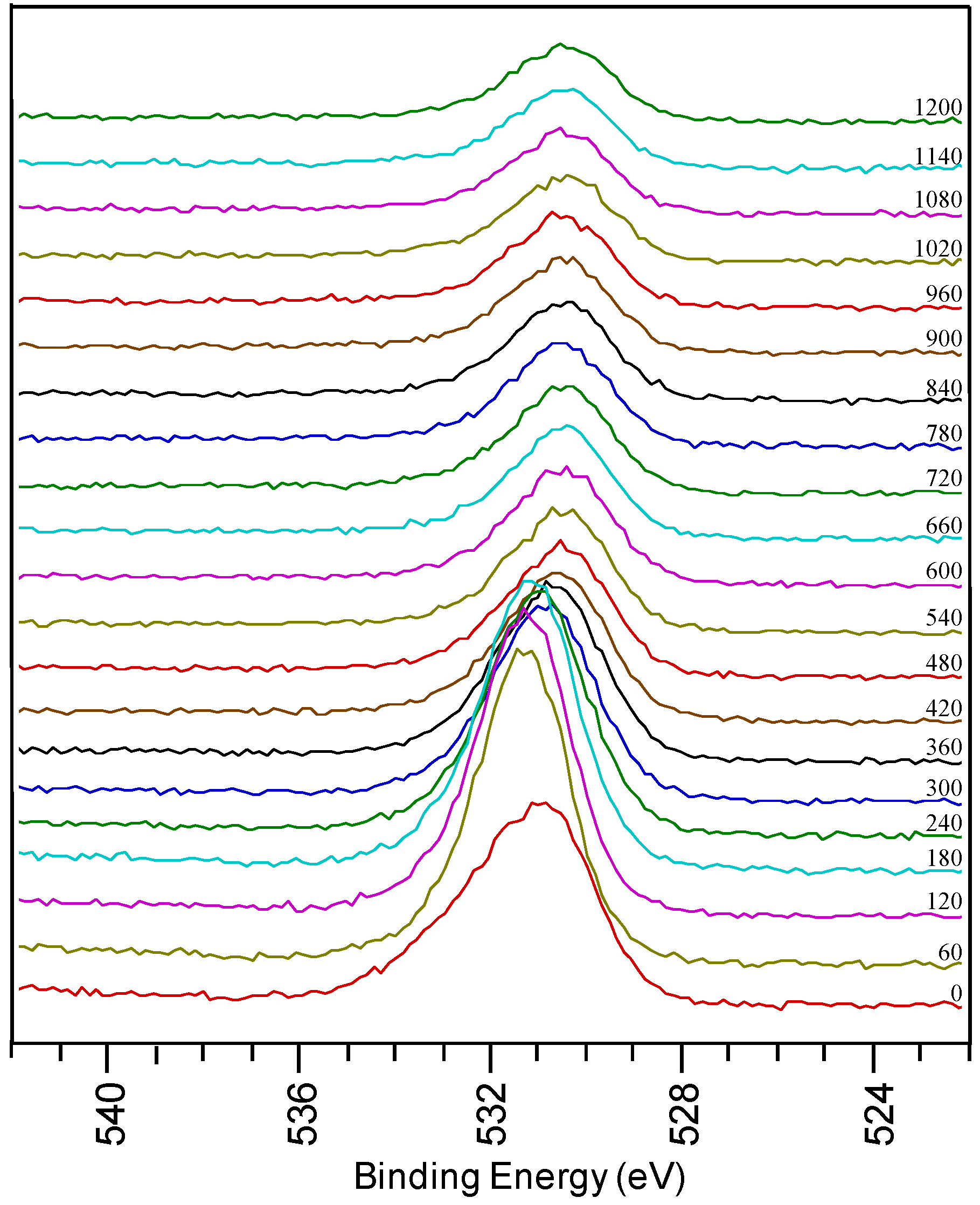
Figure 3.
O1s region from a sample using system 1 after annealing.
Figure 3.
O1s region from a sample using system 1 after annealing.
In the detailed O 1s spectra measured on a thin film prepared by system 1 after annealing, a broad oxygen peak is observed on the surface of the sample. It can be deconvoluted into a peak at low binding energy assigned to surface contamination and a peak at high binding energy corresponding to LZO. There is a shift in the oxygen peaks at different depths of the sample, corresponding to the various oxides present. With sputtering, the intensity of the peak at 531.5 eV decreases when La and Zr concentrations diminish. It shifts towards 530.5 eV indicating that oxidized Ni is present in the inner part of the sample. During annealing the physical property of the sample also changed from shiny texture (as-prepared LZO layer) to a hazy, and mildly peeled off layer (under YBCO conditions). From the high percentage of oxygen in the inner part of the sample and the shift in oxygen peak position it can be concluded that during the annealing process the substrate is severely oxidized, confirming the observations made by Cloet
et al. by TEM [
16].
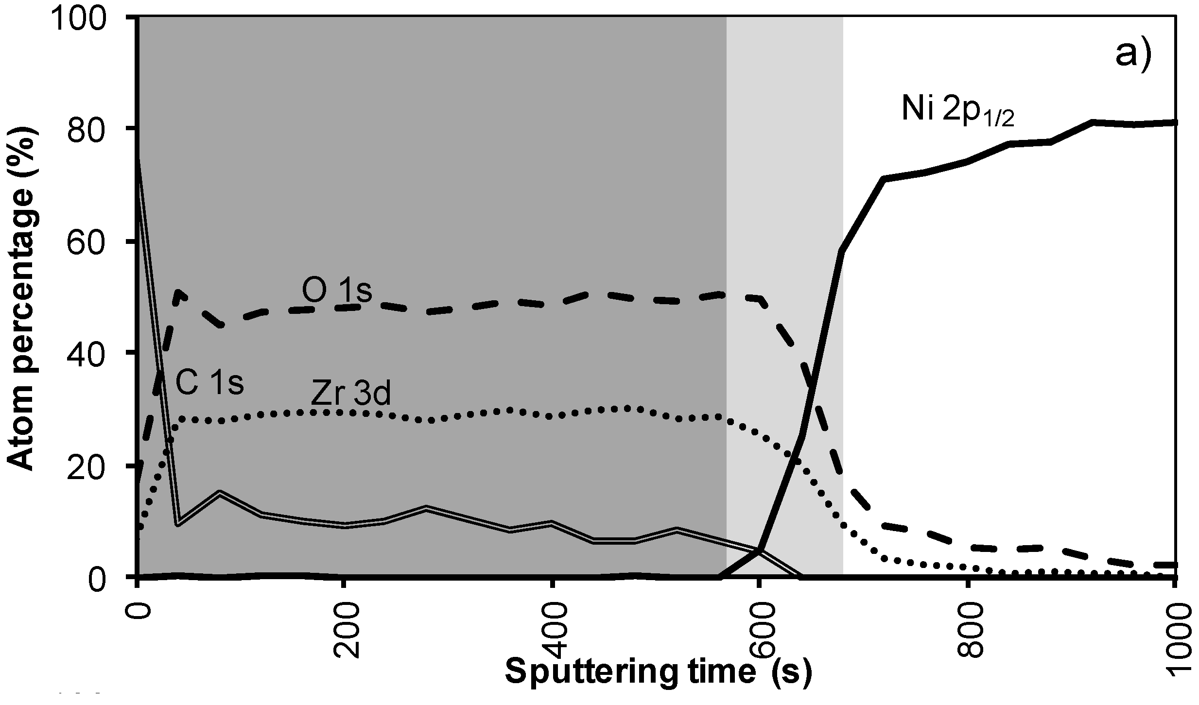
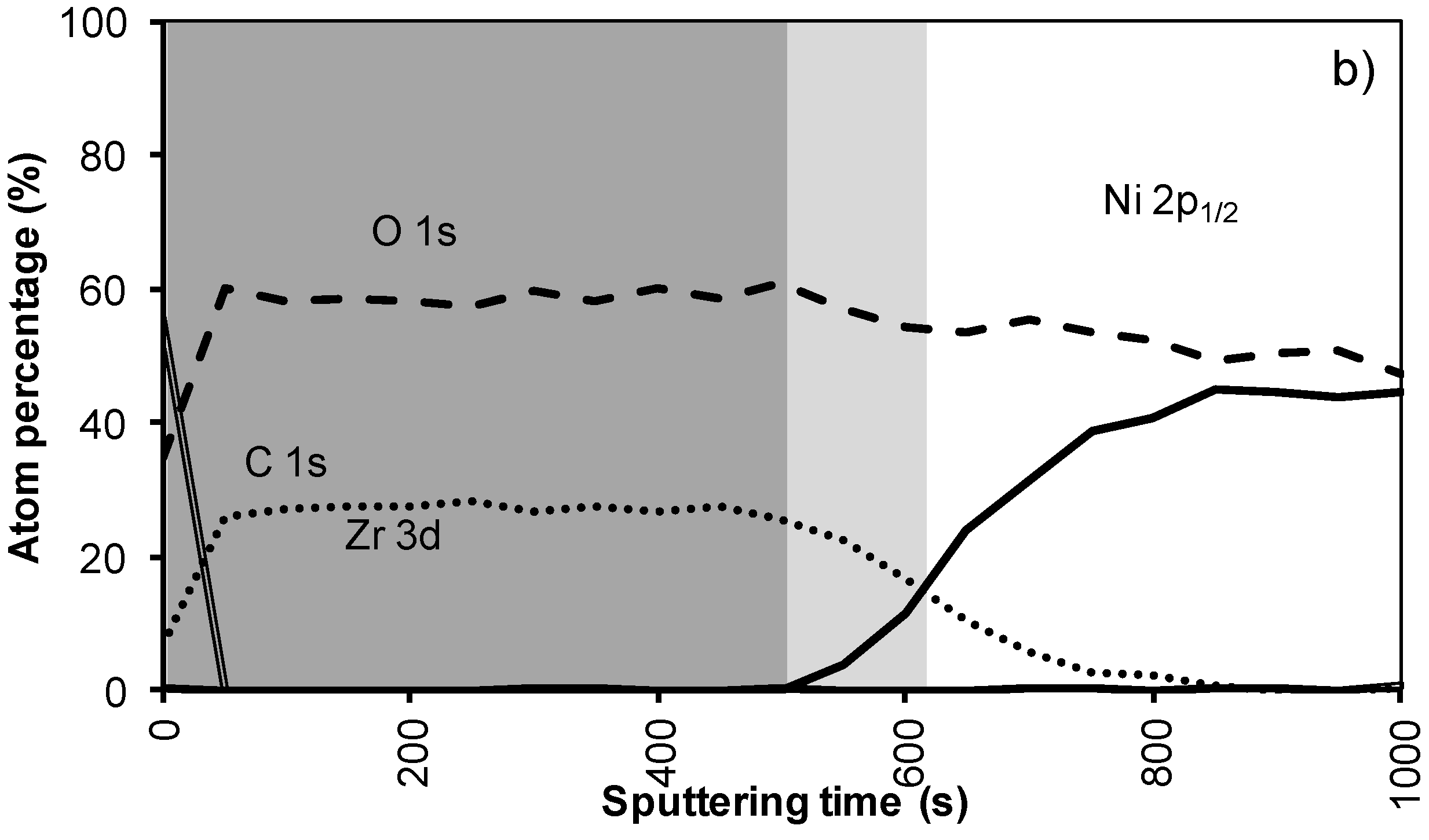
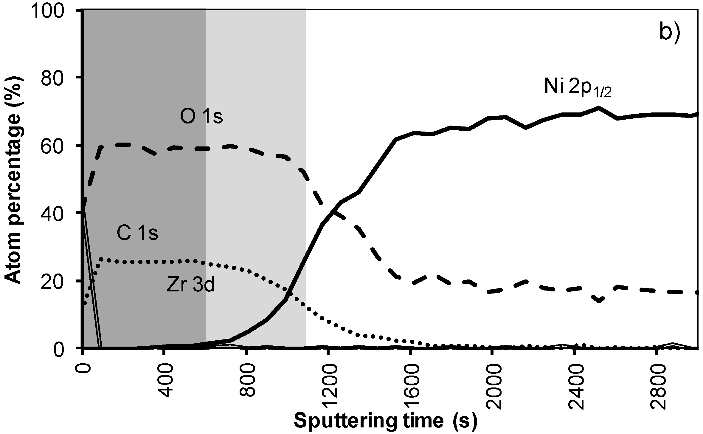
Figure 4a shows the XPS depth profile of the sample prepared with system 2 before annealing. The increased viscosity resulted in a thicker oxide film. As could be expected from ellipsometry and TEM measurements, the LZO film and thus the nickel free zone is now much thicker. The first nickel peak appears in the spectrum after 560 seconds of sputtering. Another 100 sputter s later the concentration of Zr drop towards half the maximal value. The thickness of the LZO layer is confirmed to be approximately 110 nm thick. The spectra are free of Nickel during the first 560 s
. After annealing this sample shown in
Figure 4b, again, the diffusion of Zr into Ni and vice versa vastly increased. The position at which the nickel concentration steeply increased is reduced from 100 to 85 nm (560 to 500 s respectively). In the mean-time the carbon content inside the layer disappeared. Presumably it was oxidized by the penetrating oxygen.
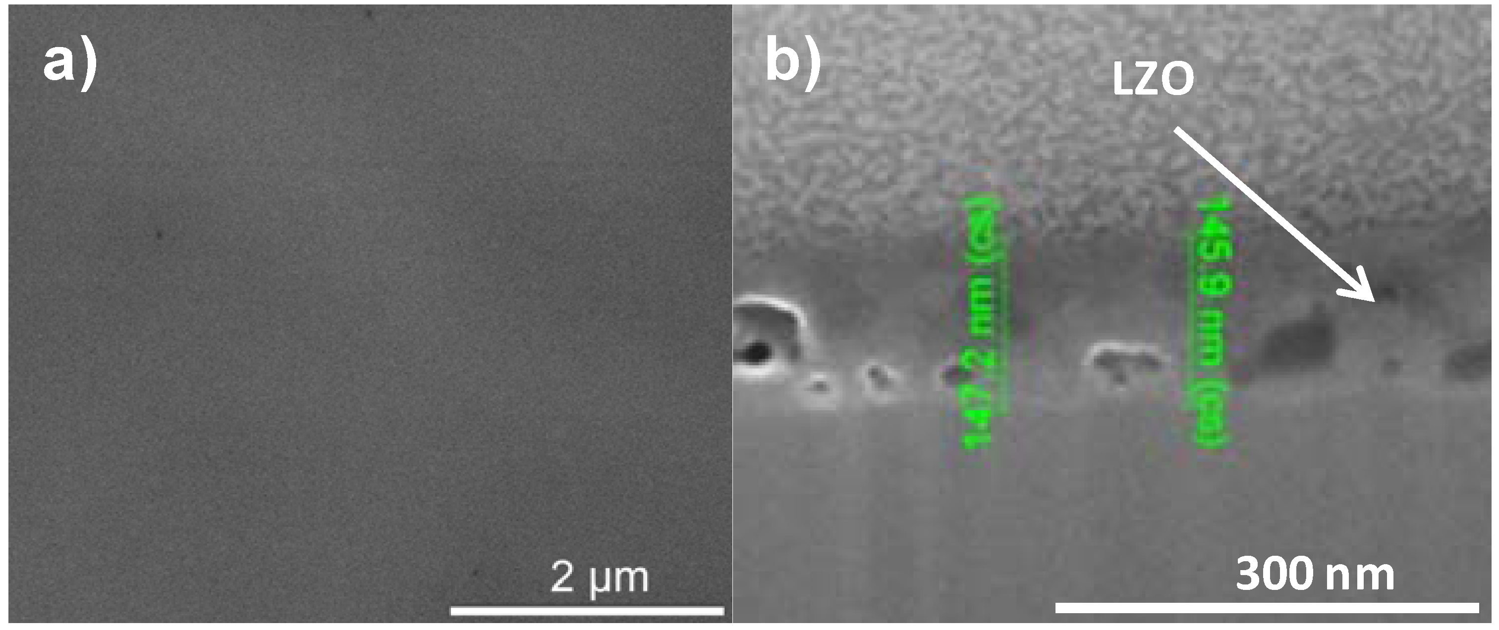
In order to increase the critical thickness of the layers and the final nickel free zone after annealing, polyvinyl pyrrolidone (PVP) was added to the sol. System 3 is similar to system 2 but the addition of PVP increased the viscosity of the sol to 5.7 mPa.s and the layer thickness after dipcoating is at least doubled. Ellipsometry shows a layer thickness of 280 nm while FIB-SEM (
Figure 5a) showed local thicknesses of 205–225 nm. Unfortunately, during the thermal process gases get trapped into the solution-gel system and the resulting layer exhibits a high porosity (
Figure 5b) compared with
Figure 1a. Those pores were present throughout the entire layer.
Figure 4.
XPS depth profile of a buffer layered sample using system 2 (a) before and (b) after annealing.
Figure 4.
XPS depth profile of a buffer layered sample using system 2 (a) before and (b) after annealing.
Figure 5.
(a) Cross-sectional FIB-SEM micrograph; (b) SEM micrograph of the top surface of a sample prepared by system 3 before annealing.
Figure 5.
(a) Cross-sectional FIB-SEM micrograph; (b) SEM micrograph of the top surface of a sample prepared by system 3 before annealing.
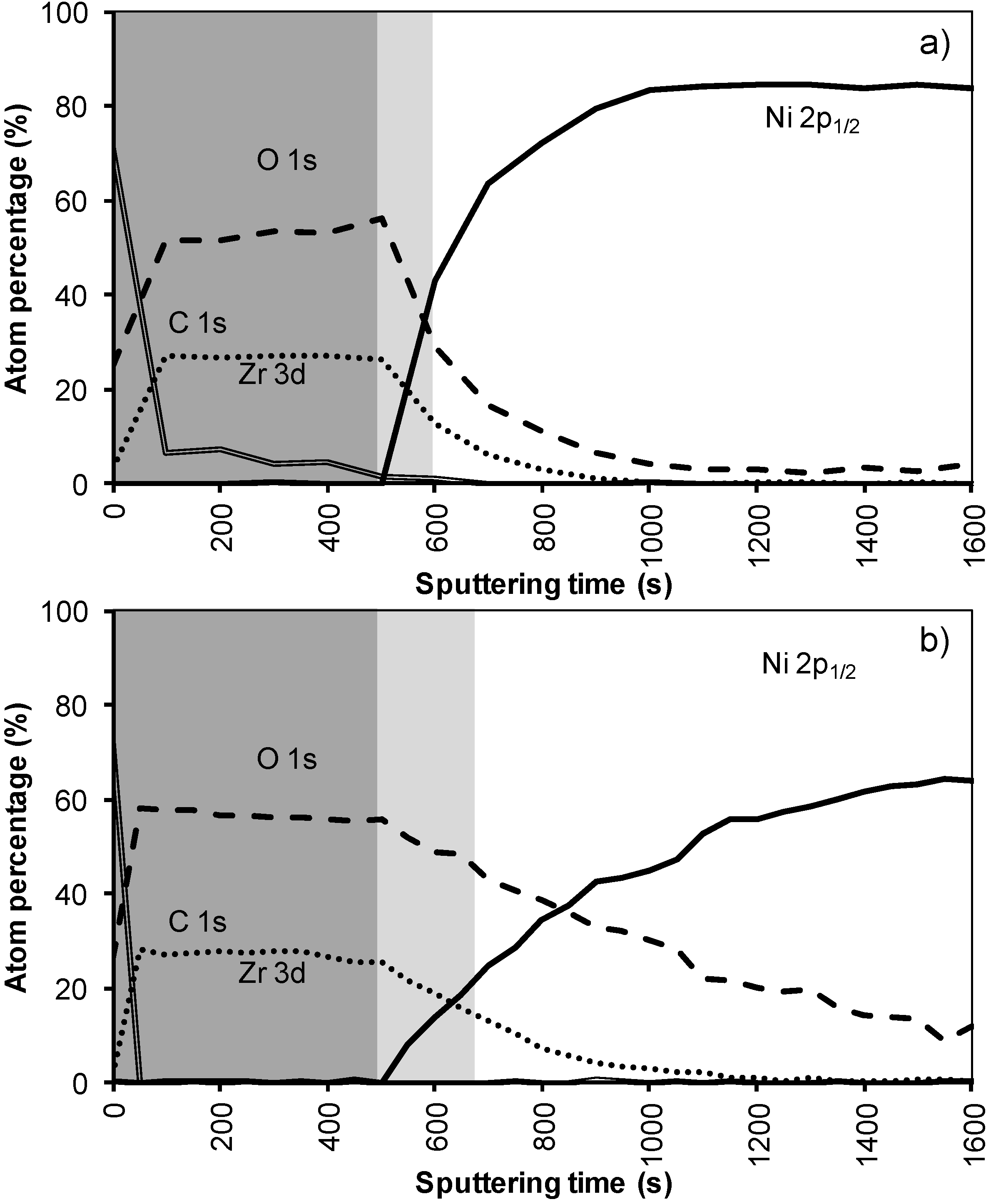
In the XPS depth profiling (
Figure 6a,b) of samples prepared by system 3, the first nickel peaks are observed after 120 nm (720 s). During annealing the nickel containing zone shifts with at least 30 nm (180 s). The increased thickness of the Ni free zone is related to the thicker LZO layer but the poor morphology causes an important reduction of the buffer capacity by 30% after annealing. A more dense but still thick enough LZO layer could lower the Ni penetration after annealing.
Figure 6.
XPS depth profile of a buffer layered sample using system 3 (a) before and (b) after annealing.
Figure 6.
XPS depth profile of a buffer layered sample using system 3 (a) before and (b) after annealing.
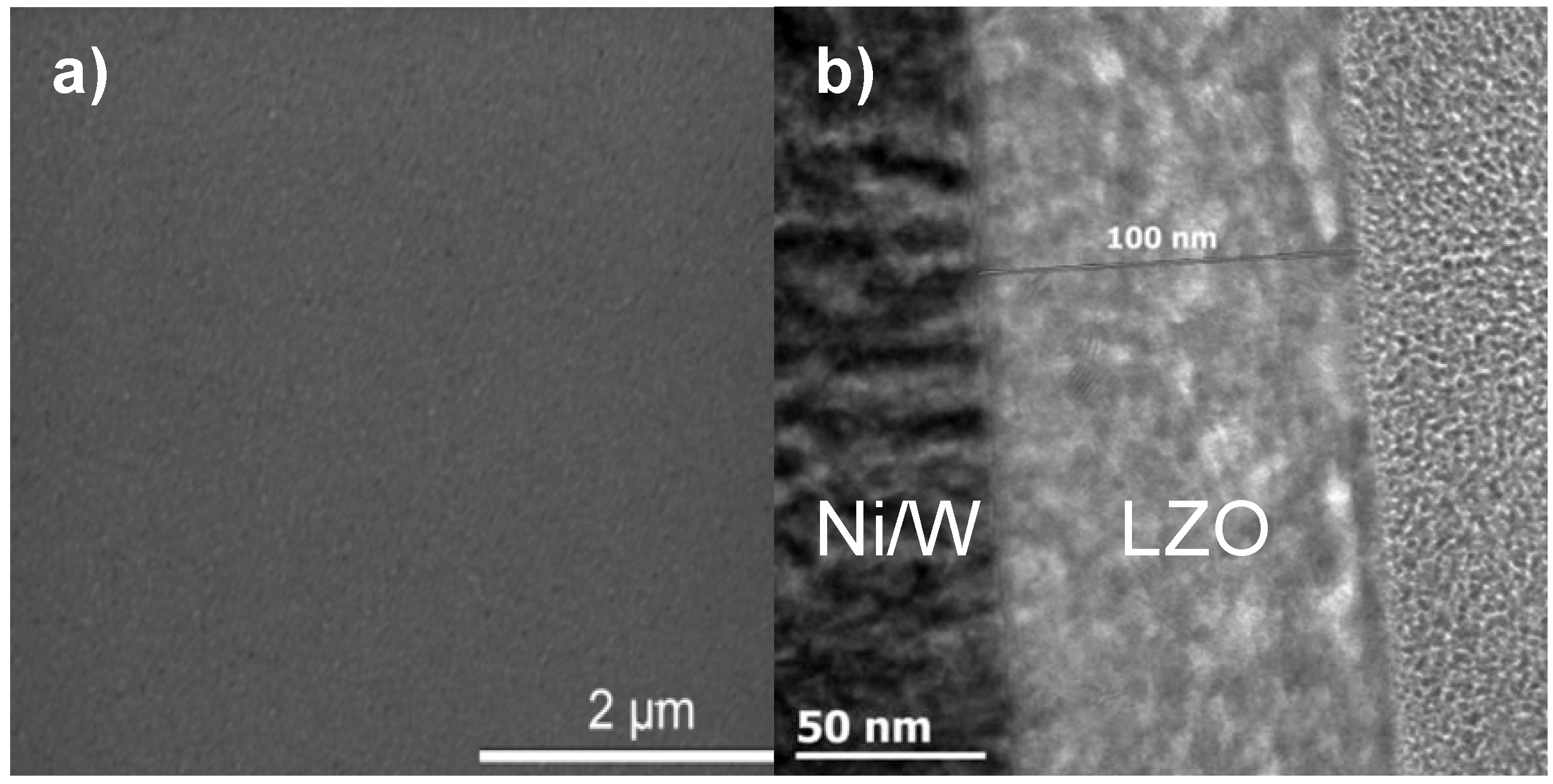
A dense, crack free film, with an intermediate thickness could be synthesized by using PVP but replacing ethylene diamine and ethylene glycol by AMP. This results in a precursor solution (system 4) with an intermediate viscosity of and a resultant layer thickness between 125 and 150 nm. SEM and FIB-SEM analysis on this sample confirmed that gases now could escape from the gel and a dense, crack-free top surface of the film was created as can be seen in
Figure 7.
Figure 7.
SEM micrograph of the (a) top surface and (b) cross section of a sample prepared by system 4 before annealing.
Figure 7.
SEM micrograph of the (a) top surface and (b) cross section of a sample prepared by system 4 before annealing.
The XPS depth profile of a film synthesized using this sol gel system 4 is shown in
Figure 8. Before annealing the nickel free zone is estimated to be 85 nm (500 s) which is in the same order as system 2. As in all previous samples annealing results in an increase in oxygen content in the interior of the sample, pointing to the formation of NiO, removal of carbon and an increased interdiffusion of the adjacent layers. However, it is promising that with the increased layer thickness the nickel free zone of 85 nm could be maintained after annealing. Based on the above results, it can be summarized that the performance of the water based thin film (non-polymer and polymer included) against Ni penetration is strongly dependent on its thickness and morphology. But, layers from all these systems do not completely withstand the oxidizing condition under YBCO annealing completely as they are showing partial oxidation through the layers.
Additionally it has been shown that the film, prepared by system 4, is an appropriate buffer layer for the preparation of an YBCO coated conductor as a highly resembling film was used as a buffer layer for depositing an YBCO thin film by metal-organic decomposition (MOD) [
19]. A buffer layer prepared by system 4 shows that CSD layers prepared by a well defined water-based chemistry can result in buffer layers preventing Ni diffusion and Ni oxidation.
Figure 8.
XPS depth profile of a buffer layered sample using system 4 (a) before and (b) after annealing.
Figure 8.
XPS depth profile of a buffer layered sample using system 4 (a) before and (b) after annealing.


