A Review on Resistive Switching in High-k Dielectrics: A Nanoscale Point of View Using Conductive Atomic Force Microscope

Abstract
: Metal-Insulator-Metal (MIM) structures have raised as the most promising configuration for next generation information storage, leading to great performance and fabrication-friendly Resistive Random Access Memories (RRAM). In these cells, the memory concept is no more based on the charge storage, but on tuning the electrical resistance of the insulating layer by applying electrical stresses to reach a high resistive state (HRS or “0”) and a low resistive state (LRS or “1”), which makes the memory point. Some high-k dielectrics show this unusual property and in the last years high-k based RRAM have been extensively analyzed, especially at the device level. However, as resistance switching (in the most promising cells) is a local phenomenon that takes place in areas of ~100 nm2, the use of characterization tools with high lateral spatial resolution is necessary. In this paper the status of resistive switching in high-k materials is reviewed from a nanoscale point of view by means of conductive atomic force microscope analyses.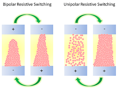
1. Introduction
High-k materials were initially used in the semiconductors industry as gate oxide in Metal-Oxide-Semiconductor Field Effect Transistors (MOSFET) [1–3], but with time, the electrical tests to which high-k materials were subjected revealed unexpected properties that extended their use to other applications. It has been observed that, when polarizing some high-k stacks under specific electrical stresses, the dielectric breakdown (which normally implies the failure of the device) can be recovered [4–6]. In other words, the insulating properties of the dielectric can be tuned by applying specific electrical fields. This unusual property, called resistive switching (RS), is revolutionizing the field of Non-Volatile Memories (NVM), significantly improving the performance of Resistive Random Access Memory (RRAM) [7,8]. Unlike NAND Flash RAM (the popular memory device we use in our memory sticks), which stores data in a little cloud of electrons in a quantum well, RRAM stores information through changes in the resistance of a cell. Avoiding charge storage is necessary to minimize the power consumption of the entire device due to leakage currents. Therefore, in this novel cell the memory concept is based on the resistance change of a relatively simple Metal-Insulator-Metal (MIM) structure [9]. The switching effect between a high resistive state (HRS or “0”) to a low resistive state (LRS or “1”) makes the memory point. The main advantages of these new-concept memories are: (i) low energy transitions. A recent study has shown that the dissipated power required for the write and read processes in RRAM is in the mW and μW range (respectively) for large devices [10]. If, in the worst case, transition pulses of 100 ns are considered, this leads to write energies in the order of 100 pJ/bit, which is very low compared to other NVM technologies; (ii) high switching speeds. Even if the reset process seems to happen slower than the set for many kinds of RRAM [11,12], transition speeds up to ~1 ns have been readily achieved [13,14]; (iii) long cycling endurance. Despite the physical origin of the RS is still unclear, engineers have been able to perform fatigue tests for these cells that showed repetitive and high RON/OFF ratios during more than 106 cycles [6,7]; (iv) excellent scalability. The different approach to store information based on the resistance change makes that scaling down of the entire cell is linked to the area where the RS takes place. As will be explained later, in the most promising RRAM the RS is based on the dielectric breakdown (BD) of the oxide, which is a local phenomenon. That makes fabricating squared memory cells, with sizes below 12 nm × 12 nm, possible [13]; (v) friendly fabrication process. The semiconductor industry has been fabricating metal-insulator junctions since the sixties, and many of the oxides being considered as insulator (HfO2, TiO2, Al2O3) are compatible with the widespread Complementary MOS technology [1,2]. All together, these factors are leading to RRAM being considered as the main candidate to replace the omnipresent NAND Flash RAM [15], and leading companies, such as Panasonic and IMEC, have already presented their RRAM prototypes.
To date RS has been widely observed at the device level in MOS and MIM capacitors using a semiconductor parameter analyzer (SPA) and the probestation [4–8]. Using this methodology the relationship between RS and some manufacturing parameters, such as oxide thickness, electrodes materials, doping impurities, and even other functioning conditions, such as voltages, current limitation, and temperatures have been addressed [16–24]. The electronic signals collected with the probestation are related to the whole area under test and, despite the fact that they give an excellent picture of the device performance, nanoscale analyses are necessary to fully understand the switching mechanisms involved. In this sense, the electrical modes of an atomic force microscope are very powerful tools to in situ analyze RS, not only from localized spectroscopic measurements, but also from current maps. In this work, the state-of-the-art on nanoscale observation of resistive switching in high-k materials using AFM related techniques is reviewed, and the correct habits for a reliable characterization using electrical modes of AFM are presented.
2. Resistive Switching in High-k Materials
The core of resistance-change memory devices consists of two electrodes sandwiching a thin stack of a material that has the property of altering its electrical resistance. Depending on the material used, these kinds of memories can be classified in three groups [9]. The first is called phase-change memory devices, and uses a chalcogenide material (for example Ge2Sb2Te5) for the switching. In this device, an electrical signal is applied to melt the chalgogenide and, depending on the duration of the stress, the chalgogenide can melt into crystalline low resistance or into amorphous high resistance states [15,25]. In the second group, called programmable metallization cells, electrical signals of opposite polarity are applied to an electrolyte glass matrix with metal ions embedded (for example Ag or Cu in GeSe). The different polarities induce the reduction and oxidation of the metal ions, leading to the creation and destruction of a nanoscale metallic protrusion that forms a bridge between the two electrodes [26,27]. The third group of materials with alterable conductivity is transition metal oxides (TMO), ranging from perovskites, such as SrTiO3, to binary oxides, such as NiO, and includes high-k materials [28–30]. Depending on the physical origin of the switching in these materials, two subgroups can be formed. In the first subgroup the mechanism for the switching has a distributed nature. In these materials, when electrical stresses of different polarities are applied, they produce the movement of charges inside the TMO to form or dissolve a Schottky barrier [31,32]. The second subgroup is based on the formation/destruction of a conductive filament (CF) between the two electrodes [5]. This working principle is similar to the one of programmable metallization cells, but, in this case, it is widely accepted that the CF is formed by high densities of defects in the insulating film. Most of the high-k materials with the best RS properties belong to the category of TMO and show filamentary conduction.
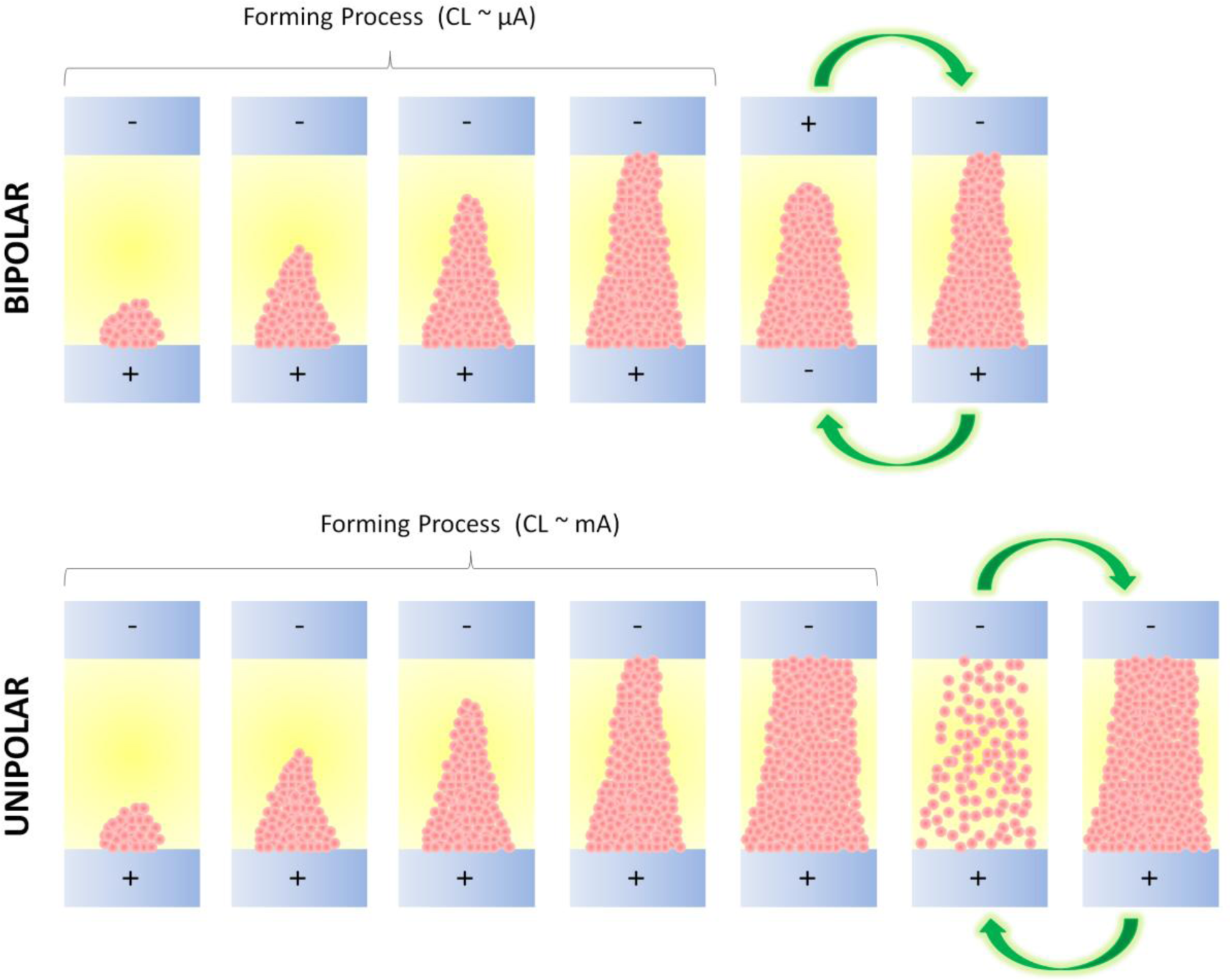
In high-k materials, the nature of CF-based RS shows many similarities to the reversible dielectric breakdown (BD) previously observed in traditional insulators like SiO2. It is widely accepted that the oxide BD is the consequence of the degradation of the insulator microstructure, which is related to the generation of defects during operation conditions [33]. When the density of defects in the oxide reaches a critical value, there is a connection of the electrodes through a defect-related conduction path within the dielectric, which leads to a sudden increase of the current through the cell (percolation model [34–36]): this is the onset of the BD and, in the field of RRAM, is usually referred as CF electroforming (forming process). The percolation model also predicts that BD takes place in areas of about 100 nm2. Initially, it was believed that the BD was irreversible but later it was observed that, under specific polarization conditions, this conductive filament could be partially destroyed (reset process). The observation of RS normally requires: (i) the use of a current limitation (CL) during the forming process to control the amount of defects generated in the dielectric. If no current compliance is used during the forming, dramatic BD lateral propagation, electrochemical metallization, and Dielectric Breakdown Induced Epitaxy (DBIE) can take place and the BD becomes irreversible [37,38], showing currents orders of magnitude larger than in LRS [12,39]; and (ii) the application of an additional electrical stress to induce the reset process. When the reset takes place by applying an electrical stress of the same polarity than the one used during the forming, the RS is called unipolar, and when both set/reset processes require inversed polarities the RS is called bipolar [31]. It is also worth noting that both switching mechanisms may also coexist in some materials [40]. In those cases, the key factor that determines the presence of one, the other, or both simultaneously is the current level at which the CF was formed. At low CLs a thin CF formed by oxygen vacancies that migrate from anode to cathode is formed between the two electrodes [41]. It is even known that the CF has a cone-like shape with the narrower part at the cathode side [5,42,43]. This CF can be easily reoxidized at its narrower end by applying a reverse voltage, leading to bipolar RS [31]. If the CL used during the forming is too high, the oxygen vacancies based CF is too thick to be reoxidized, and it may also contain impurities from the adjacent metallic layer; in this case, the only way to destroy it is using higher currents to produce a thermal heat that fuses it [31,44,45]. Figure 1 shows a schematic of both RS mechanisms. Despite the fact that unipolar RS shows some advantages, such as higher LRS/HRS current ratio and simplicity of peripherical circuits, it is evident that it implies larger power consumption per resistive state transition, which is making many researchers and companies shift their attention to bipolar RS.
3. Methodologies for a Correct Observation of Resistive Switching at the Nanoscale
As mentioned, in high-k thin films the diameter of the conductive filament formed between the top and bottom interfaces is around ~100 nm2. Therefore, to provide in situ information about its formation and rupture, the use of characterization tools with high lateral resolution are necessary. The most widespread techniques in nanoscale electrical characterization are Scanning Tunneling Microscope (STM) and the Conductive Atomic Force Microscope (CAFM). Even if it requires the use of a conductive sample, STM has been successfully used to assess fluctuations of local conductivity of thin high-k insulating films. The group headed by Pey [46] collected IV curves and current maps on the surface of polycrystalline CeO2, reporting that the current through the grain boundaries was larger. Chen et al. [47] even observed cyclic resistivity changes in Nb-doped SrTiO3 using STM. It is worth noting that the current signal obtained in STM corresponds to the tunneling current that flows between the tip and the sample when the separation between them is of just a few nanometers. Therefore, the tip is not in contact to the sample, which adds a resistive component to the tip-sample system. This problem is avoided when using the CAFM working in contact mode, which provides topographic and electrical information about the sample simultaneously. CAFM has been readily used to analyze the electrical properties of gate oxides since the 1990s [48–50], and, in the field of high-k CAFM, has provided much key information. For example, some works pointed out that the native density of defects in high-k materials is higher than in SiO2, which favors the conduction by trap-assisted tunneling, increasing the leakage current [51]. CAFM also helped to demonstrate that an optimized post-deposition annealing significantly reduces charge trapping in HfO2 layers [52], which has a remarkable influence on their reliability. Other authors [53] indicated that SiO2 doping in crystalline high-k dielectrics significantly increases the electrical uniformity and minimize leakage currents. All this information has been gained from spectroscopic IV curves and topographic-current maps by applying a voltage to the bottom of the sample and grounding the tip (and vice versa); however, the study of RS with CAFM is much more complex and the observation of some phenomena, such as the forming, reset, and set processes requires the application of sequences of specific stresses. From the literature it is possible to see that mainly three methodologies have been used to observe RS in high-k materials. Every method has its own advantages and drawbacks, and, here, it is recommended to select the most convenient method depending on the sample under test and behavior to be analyzed.
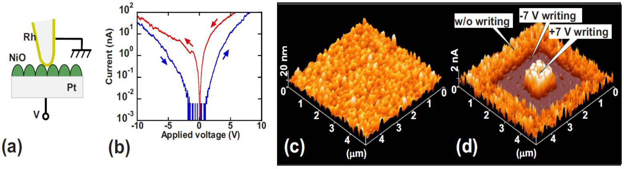
The first method consists of inducing the set or reset process at the device level in a traditional MIM structure, and then etch the top electrode and scan the bare surface of the insulating stack with the CAFM using a low voltage that simulates a read operation. The first notable study in this direction was performed by Choi et al. [54], in which some Al/TiO2/Ru capacitors were pre-stressed to write the HRS and LRS. Then, the Al top electrodes were etched away by a nitric acid solution, and the surface morphology and local conductivity of TiO2 films below the Al electrodes were investigated. The high lateral resolution of the CAFM revealed that the amount of conductive spots in the LRS cell is larger and they also drive larger currents. As the current images in their paper are displayed with different current scales, exact spot size comparison is not possible, but it is evident that the conductive spots in HRS are smaller. This pioneer experiment was used by other researchers to determine the RS behavior in different materials. Son et al. [55] used this method to analyze the current, size, and amount of leaky sites generated in two Hg/NiO/Pt nanocapacitors (one in LRS and the other in HRS). Thanks to this methodology he observed that the NiO stack in LRS contained more leaky sites than the one in HRS, and that their sizes and currents are larger (Figure 2). Moreover, by comparing topographic and current images the authors determined that the structure of the NiO layer is polycrystalline, and that the conductive spots are mainly located at the grain boundaries.
This methodology easily allows performing accurate statistical analysis of the conductive filaments generated in both resistive states. To do so, after the current maps are obtained, the resulting images are processed off-line with the software of the AFM. A critical step when analyzing the spots size is the selection of the threshold current. The particle analysis tool of most of AFM software (Nanoscope for Bruker, Picoview for Agilent, WSxM for Nanotec [56], and others) requires the selection of a current limit, which, due to the large differences of the currents driven by the filaments in HRS and LRS, could have different values for each state. Then, all pixels of the images will be shown in a Bolean-like picture, indicating whether if each pixel current is higher than the threshold or not, and they will be grouped by their X-Y position to find out island-like configurations. These islands correspond to the top view of the conductive filament through the insulator, and the AFM software can provide valuable information about them, such as the size, maximum current, and volume. A good example is the recent report from Sigh et al. [57], where the area and current driven by conductive filaments of both resistive states in Ti/CuO2/Cu capacitors is addressed (Figure 3). In that case, the top Ti electrode is etched by Focused Ion Beam (FIB), and a read voltage of 2 V is used to scan the bare surface of the insulators in HRS and LRS. It is worth noting that read voltages in CAFM experiments are usually larger than at the device level due to the much smaller area under stress at the nanoscale. Thanks to this methodology the authors found out that larger MIM capacitors show larger density of stronger CFs (Figure 3), which are difficult to rupture and correlate to the higher reset voltages observed at the device level.
Even if this method has the advantage that the LRS/HRS state are induced using real structures, a very selective etching method to remove the top electrode is necessary, and the chemical etchant may affect the composition of the CF and insulator surface. Wet etching and FIB are among the most common etching methods [57,58]. Celano et al. [59] removed the top electrode in TiN/HfO2/Hf/TiN capacitors by carefully scratching the top electrode using homemade diamond tips and commercial boron doped diamond-coated tips with high spring constants, observing reasonable LRS/HRS current ratios and spot sizes. On the other hand, this analysis provides statistical information about the nature of CFs in HRS and LRS, but the properties of a single filament in both states cannot be analyzed: the maps in HRS and LRS correspond to different capacitors. In addition, the kinetic electrical signals collected at the device level do not represent the current through a single CF, but they apply to the whole area of the capacitor.
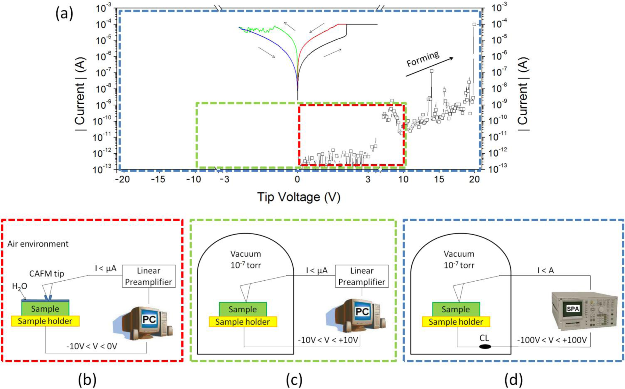
The second methodology is to induce the set and reset processes by applying Ramped Voltage Stresses (RVS) with the tip of the CAFM directly on the bare surface of the insulating stack, and then scan the surface in a similar read-like way. This method permits not only the in situ observation of the CF in each state, but also to analyze the evolution of the electrical properties of single CFs depending on the applied bias. Moreover, following this methodology, one can be totally sure that the current collected corresponds to the one flowing only through the CF under the CAFM tip. The group headed by professor Waser was the first in using this method, and, in their novel report, they demonstrate RS in single dislocations of SrTiO3 films [28]. However, this process also has some drawbacks. One of the most important limitations when studying RS in high-k materials at the nanoscale is that the maximum voltage most commercial CAFMs can apply is ±10 V (Figure 4c), which could be insufficient to complete the forming process (reach the BD). Moreover, most works studying filamentary RS in high-k materials reported that the reset process occurs for current densities above tens of microamperes [28,31,44,45]. The problem here is that most of commercial CAFMs can measure currents up to tens of nanoamperes, and above that level the electronics of the CAFM (linear current-to-voltage preamplifier) saturates, showing a horizontal line in the IV curves. Thus, even if the resistance change can be observed from the shifts between the forward and backward curves [28], the electronic response of the cell during the reset process is masked. One possible solution for these limitations is the use of a linear preamplifier with a configurable gain [60], but this may mask other valuable information, such as the onset voltage [61] (minimum voltage at which current above the noise level can be measured).
A better solution is to use an external SPA [12,39,62,63] or sourcemeter [28,64,65] to apply the electrical stress and measure the current (Figure 4d). It is worth noting that this methodology, developed for the first time in 2005, by professor Nafria’s group [66], has been used by other authors to analyze the dielectric breakdown of high-k materials [51,67]. This genuine setup provides another essential feature to observe RS at the nanoscale: the possibility to use different levels of CL. In [39] this methodology was used to analyze the RS characteristics of ultrathin polycrystalline HfO2 layers. Using this method, the pre- and post-BD current signals can be clearly observed, displaying a progressive reset transition. The high resolution of the technique allowed to difference two types of electrical behaviors in polycrystalline HfO2 stacks: electrically weaker grain boundaries that reached the BD at low voltages and showed RS in successive cyclic voltammograms, and robust nanocrystals where drastic propagation of the BD happened, leading to irreversible conductive filaments. Moreover, the similarities between the IV curves of a single filament and those measured at the device level corroborated that the current in LRS is independent of the device area, and that takes place at point locations of the sample. With the time, some companies started to provide new CAFM current modules with higher dynamic current ranges, such as the Resiscope mode from Agilent [68], but there is still a lack of works showing the kinetics of the reset process with CAFM. Another necessary capability for the CAFM when measuring bipolar RS is the use of an environmental chamber (Figure 4c,d). It is widely known that the injection of electrons from the CAFM tip can reduce the current through the high-k material due to anodic oxidation [69]. To avoid this problem, it is necessary to measure in dry nitrogen or in high-vacuum environments [39,70]. Finally, this method provides information about one single CF, and getting statistical data may be difficult due to tip wearing.
The last method consists of inducing the set, reset and read operations from current maps. Yoshida et al. [71] was one of the first researchers that used this methodology. In that case, he performed sequences of current maps with different sizes and voltages centered at the same point of a NiO stack (Figure 5). The areas scanned one time corresponded to HRS, showing lower densities of smaller CFs that drive lower currents, while the areas scanned two times correspond to LRS, showing larger densities of bigger CFs that drive higher currents. Later works performed set-read-reset-read sequences of current maps where the increase of the size and current of many single CFs could be perfectly observed. Zhou et al. [72] performed a similar analysis using the same scan size in CuOx layers. It is worth noting that in these works the current maps have been collected without any CL, and here it is recommended the use of an external current-limited sourcemeter or SPA to apply the voltage as in [12]. This methodology is specially suitable to analyze materials with low forming voltages, such as NiO or CuOx, as the movement of the tip increases its wearing even more than in IV curves.
Even if this method does not provide kinetic information about the set/reset process, it provides statistical information of single CFs in both HRS and LRS. Probably the most tricky part of this method is the correct selection of the set and reset voltages (VSET and VRESET respectively). Due to the intrinsic inhomogeneities of the sample (defect concentrations, fluctuations of the physical thickness, etc.) VSET and VRESET may vary from one location to another. These inhomogeneities can produce that, for example, when applying a specific VRESET to destroy some CFs, new CFs could appear at weaker locations [12]. In many cases, this may be a minor problem because these new spots could be easily detected from one scan to the other. Moreover, the larger areas scanned by the tip make possible the use of other techniques (like X-ray Photoelectron Spectroscopy or Auger Electron Spectroscopy) to analyze the chemical changes induced during the transition, which is not possible when forming the CF with a CAFM IV curve (due to the local nature of the BD) [71–73].
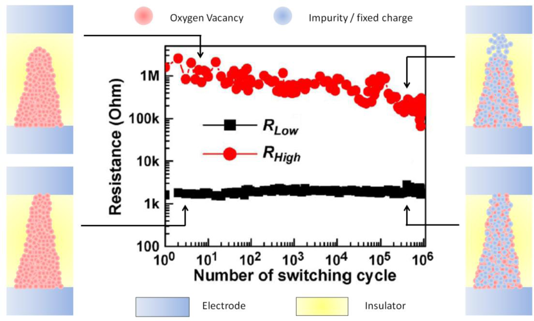
It is important to highlight that the durability of the RS effect in high-k materials is strongly linked to the movement of oxygen vacancies or, in other words, to the absence of non-mobile impurities. With each RS cycle performed, impurities from the adjacent layers may penetrate in the insulating stack, increasing the current in HRS. After several cycles, the density of impurities can be so high that the CF could not be reoxidized anymore (Figure 6), leading to the failure of the cell because HRS and LRS cannot be distinguished [7].
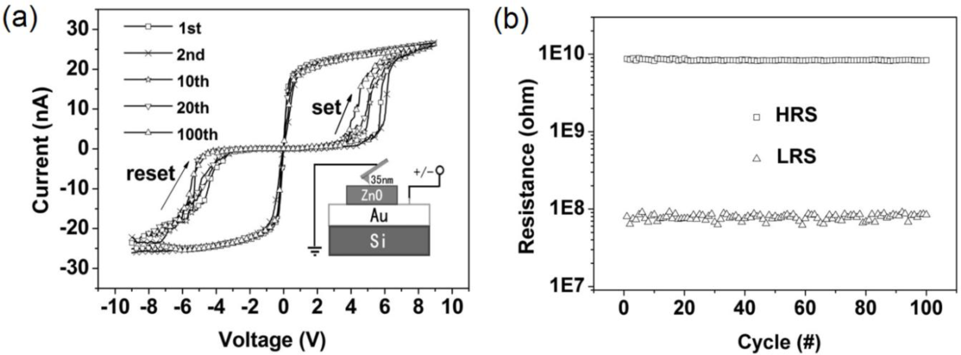
On the other hand, it is widely known that the metallic varnish of CAFM tips is not very stable and, due to the high current densities involved during the switching, it may contaminate the internal structure of the CF, leading to the irreversible BD. It is worth noting that the current densities may be as high as 109 A/cm2, that is 1 mA flowing through the typical tip-sample contact area in a CAFM, which is typically around ~100 nm2. Therefore, one should be very careful when creating/destroying CFs directly with the CAFM tip. A necessary precaution when doing these kinds of experiments is to select a stable enough tip. In the market, one can find some very stable tips, such as diamond coated tips [74], ultra-sharp platinum wires [75], and, recently, prototypes of graphene-coated CAFM tips [64,65,76–78] also showed superior performance. Despite these precautions, measuring the endurance of RS at the nanoscale with CAFM is still a challenge, and more works should be conducted in this direction to analyze the reliability and variability of RRAM. The only endurance tests using CAFM found in the literature was reported by Wang et al. [79], however, that work does not really fit the experiments above as the currents measured are too low, always below ±30 nA (Figure 7), which considerably reduces the damage of the tip in every transition. Despite this, he achieved visualization of the RS transition during only 100 cycles, this is the maximum number of cycles ever reported with the CAFM.
4. In Situ Observations of Bipolar Resistive Switching
The first notable in situ observation of resistive switching was reported by Szot et al., in 2006 [28]. In that work, the tip of the CAFM was used to apply local electrical tests at single locations of SrTiO3 films. The current images show an important change in the sizes and currents driven by local conductive spots in HRS and LRS. Interestingly, sequences of IV curves reveal a change from non-linear to linear conductive behavior with a LRS/HRS current ratio of 104, indicating a change in the filament composition. It is important to highlight the localized nature of the RS, which only takes place at the leakiest locations of the sample. The comparison between current and topographic CAFM images indicates an overlap between topographic nanoaccidents and high-current paths [80]. Cross-sectional TEM images additionally suggest the presence of inhomogeneous concentrations of defect paths inside the SrTiO3 films [80]. It is commonly accepted that the defects in SrTiO3 films are related to oxygen vacancies, and that the amount can be controlled by tuning the applied voltage, leading to different resistive states. This behavior was also confirmed by laterally resolved micro-X-ray absorption spectroscopy and thermal imaging in similar memory cells, where the resistance switching originated from an oxygen-vacancy drift to/from the electrode that was used as anode during the conditioning process [81]. Later works also proved the different oxygen densities in HRS and LRS from chemical tests, such as AES and XPS peaks [82,83]. CAFM experiments revealed the localized nature of RS, which is based on nanometric conductive filaments with diameters as small as ~1 nm.
The concept of resistance change based on oxygen migration is not unique of SrTiO3, but it has been readily observed in other high-k materials, such as TiO2, HfO2, ZrO2, and TaO2 [84], and it is widely accepted that it pays a crucial role for the entire class of TMO-based bipolar resistance-change memory. Choi et al. [54] was the first to analyze the local conductivity of TiO2-based capacitors in HRS and LRS with the CAFM. To do so, first the HRS and LRS were written at the device level, and then the top electrode was etched and the surface of the TiO2 layer was scanned with the CAFM. Using this methodology, the authors observed that the density of conductive spots in the capacitors in LRS was larger. Moreover, the sizes and currents in LRS were also larger. The resistance change has also been observed by inducing the set-reset process with the tip of the CAFM [85], indicating again the localized nature of the CAFM. The Kelvin Probe Force Microscope additionally revealed a change in the contact potential difference for each resistive state, proving the movement of charge inside the dielectric [85]. ZnO is another material that traditionally showed good local resistance change behavior, but in this case the LRS/HRS current ratios observed are not as high as in SrTiO3 and TiO2. Despite the fact that many works have been devoted to study the morphology and electrical properties of this material at the nanoscale [86,87], just a few authors analyzed RS using high lateral resolution techniques. The most significant report was published by Wang et al. [79], who published the first endurance test with CAFM. In his work, the authors collected sequences of IV curves with the tip of the CAFM at random locations of ZnO blankets, observing the typical repetitive state change with current ratios of 100. It is also known that ZnO layers can be used as buffer layer between the dielectric and one of the metallic electrodes to enhance the resistive switching behavior [88], due to the high density of oxygen vacancies in it. Other high-k materials, such as Tantalum [89,90], Lanthanum [91,92], and Yttrium [93] oxides also showed good bipolar RS response under specific polarization, but they are less compatible with CMOS technology than hafnium- and aluminum-based oxides. Y2O3 is, specifically, interesting for Carbon electronics due to its great compatibility with graphene and carbon nanotubes. The report from Park et al. [93] demonstrates that graphene electrodes may eliminate mechanical stresses in the Y2O3 of NVMs, which significantly enhances the data retention properties. Unfortunately, despite the nanoscale properties of these three candidates have been studied at the nanoscale using high-resolution techniques [94], RS in such stacks has rarely been studied at the nanoscale.
The main challenge now in the field of RRAM relies on selecting the right materials that will be used to form in the MIM structure, not only the insulator but also the metals. The main goal is to optimize some parameters such as layer thickness, doping densities and operating voltages, in order to achieve cheap RRAM cells with low energy HRS/LRS transitions, high switching speeds, long cycling endurance, and good scalability. Therefore, since the simplicity and cost of the MIM structure plays a very important role for the introduction of high-k in NVM industry, many researchers explored the RS behavior of fabrication-friendly hafnium oxide.
5. Physical Origin of Resistive Switching in Hafnium Dioxide
As insulator for RRAM, hafnium dioxide deserves a section for itself because, due to its great compatibility to CMOS technologies and good performance, it is the most promising dielectric for real future applications. Most of the leading institutions in microelectronic manufacturing and research like Sematech, Globalfoundries, INTEL, Micron, Panasonic, Samsung, TSMC, Elpida, Hynix, Fujitsu, and IMEC have been studying this material during the last years, and some of them even presented their prototypes. To date, HfO2-based RRAM cells lead to the best performances ever, reaching areas smaller than 10 nm × 10 nm, excellent endurance up to 109 cycles, fast switching speeds in the nanosecond range, and power consumptions per transition of ~0.1 pJ [13,14]. In this section, the origin of RS in HfO2 stacks is analyzed paying attention to the manufacturing parameters, which strongly affect the performance of the entire cell.
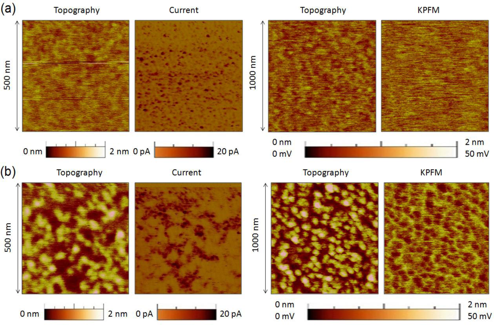
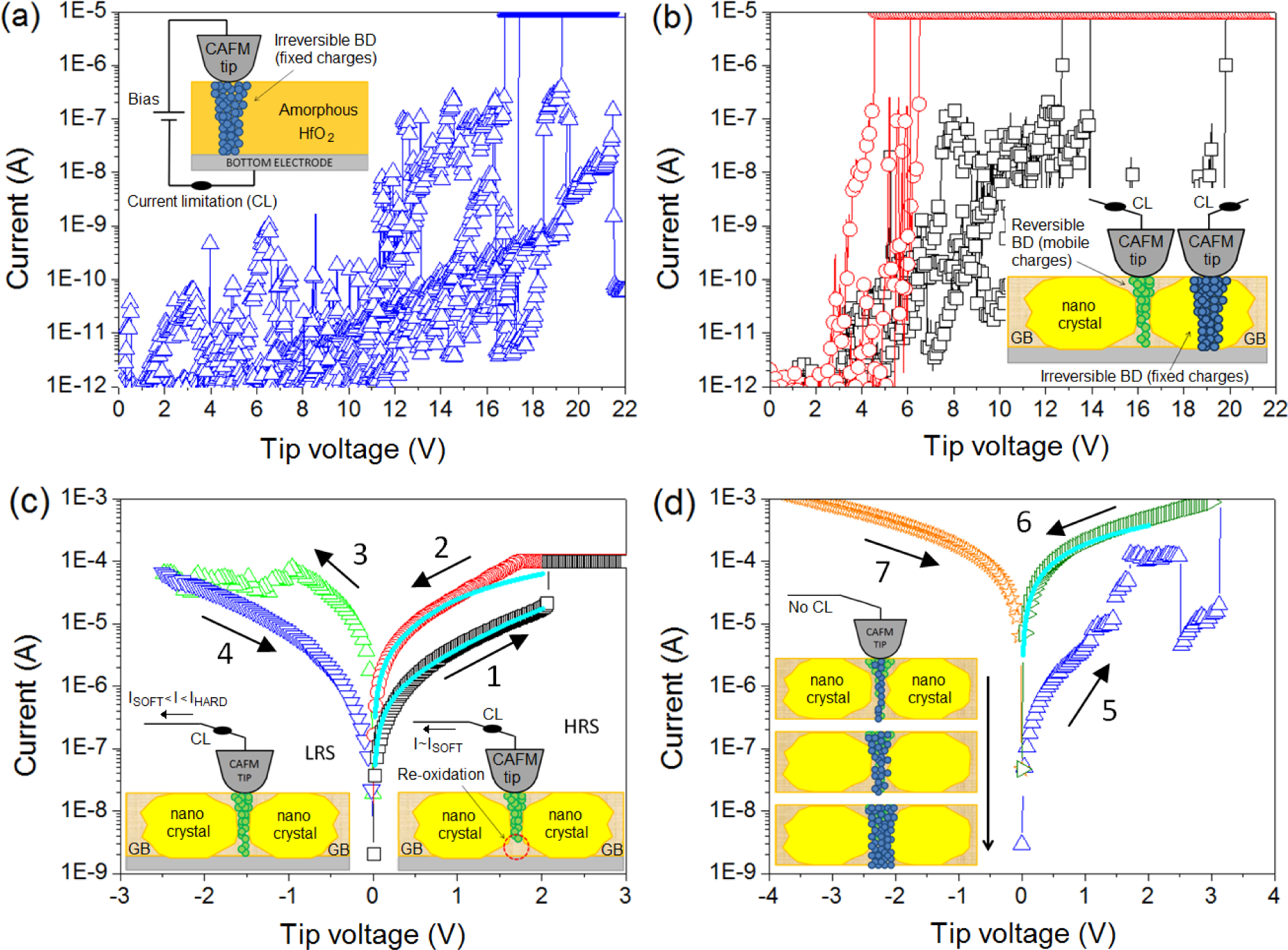
In the fabrication process of hafnium-based RRAM there is one key parameter that strongly affects the RS phenomenon: the annealing process, a thermal step, which is normally used in CMOS technology, to activate dopants and remove defects (among other uses). It is widely known that high annealing temperatures produce the polycrystallization of the high-k film [95], which has been shown to affect its electronic properties [96]. Initially, there were concerns that leakage current densities may be higher across polycrystalline dielectrics as defective grain boundary regions may enhance electronic conduction. This hypothesis was discarded by Kim et al. [97], who observed that crystallization of HfO2 films in MOS capacitors had almost no effect on the total leakage current. However, this does not means that the local electrical properties of the high-k remained unaltered after the anneal, and later works showed important local differences. Petry et al. [98] were one of the first in analyzing the effect of annealing on the nanoscale electrical properties of thin HfO2, revealing that phase change implied changes in the current homogeneity, due to both grain formation (observed with CAFM) and fluctuations of the film thickness (observed with X-Ray Reflectometry and TEM). Later works further supported these conclusions [96,99], and now there is a general consensus that grain boundaries in HfO2 are leakier [5,41,100] due to larger concentration of positive charges (defects), as corroborated by KPFM [101]. As an example, Figure 8 shows the topographic and simultaneously collected current and contact potential difference maps (CPD, collected by KPFM) measured on (a) an amorphous and (b) a polycrystalline 2.5 nm-HfO2 film on 1 nm-SiO2/Si stacks (crystallization induced by annealing at 1000 °C). Despite the thickness of each film cannot be assessed with CAFM, evident topographic, current and charge concentration changes can be clearly distinguished. Therefore, even if the total pre-BD current through amorphous and polycrystalline stacks may be similar [97] (i.e., the sum of the tunneling current though the total area of the amorphous cell may be of the same order than the one through the grains plus grain boundaries in the polycrystalline one), the fluctuations generated at the nanoscale may have an important effect on the BD characteristics, as the BD is a local phenomenon that takes place at the weakest location of the area under stress. In addition, RS studies corroborate this hypothesis: the best RS performance in HfO2 stacks has been achieved when using moderate annealing temperatures between 400 and 600 °C. At too low temperatures the breakdown voltages may be too large leading to drastic BD [12], while temperatures that are too high may damage the internal structure of the stack, leading to premature irreversible conductive filaments [100]. This behavior has been also proved at the nanoscale. By means of sequences of spectroscopic IV curves performed with Enhanced CAFM (Figure 4d) at different random locations of the sample, it has been observed that amorphous HfO2 layers reach the dielectric breakdown at high voltages, and that after the CF formation no reset process was observed in subsequent cyclic voltammograms, leading to irreversible BD even using current limitation (Figure 9a). A similar behavior has been observed at most of the analyzed locations (randomly selected) of polycrystalline HfO2 stacks (Figure 9c), and even larger currents were observed in post-BD curves, probably due to BD propagation through in the crystals of the high-k [61].
On the contrary, a singular low amount of analyzed locations in the polycrystalline HfO2 film showed genuine low BD voltages (Figure 9b), followed by repetitive bipolar RS in cyclic voltammograms (Figure 9c). The LRS currents driven by a CF formed at the weak locations were very similar to those observed at the device level, indicating that most of the current through the cell is flowing through that weak spot [58]. This result was observed in further topographic and current maps, where a correlation between the reversible filament and the grain boundary was possible [12]. These observations empirically and in-situ proved that the origin of RS in HfO2 stacks is the weaker nature of the GBs. Probably the lower BD voltage lead to a reduced damage of the internal structure of the HfO2 stack at that location, in other words, to a thinner filament easier to reoxidize in subsequent cyclic voltammograms. KPFM results [101] indicate that the leakier nature of the GBs is related to a larger concentration of charges at those locations, and chemical tests and theoretical calculations indicate that those charges are related to oxygen vacancies.
The difficulty of observing RS at the nanoscale with the tip of the CAFM relies on the problem of placing the tip on a grain boundary. First, grain boundaries in HfO2 are as thin as 1 nm [102] which is an area in the limit of the lateral resolution of the CAFM, even measuring in vacuum, which provides better spatial resolutions by removing the water meniscus formed between the tip and the sample [70]. It has been estimated that GBs cover an area below 10% of the HfO2 stack [100].
Second, in many cases grain boundaries cannot be observed from CAFM topographic maps. Figure 10 displays the schematic and typical topographic and current maps for HfO2 stacks with different annealing. Polycrystallization of the HfO2 layer not necessarily implies drastic topographic modification [98], which makes difficult to distinguish the grain boundaries in topographic maps (Figure 10b). Those samples where the grain boundaries can be clearly observed in topographic maps are those in which open grain boundaries were formed (Figure 10c), which refer to a local damage of the sample that produces the reduction of the layer thickness [100] and the formation of a permanent conductive path at the GBs. In such case, resistive switching has never been observed as the conductive path cannot be ruptured. Third, the degree of crystallization also depends on the thickness of the HfO2 layer [12,61,95], which produces that two stacks of different thicknesses, annealed at the same temperature, may have different degrees of polycrystallization. This may also generate some confusion when comparing results. In addition, fourth, the environment, current limitation and stability of the tips used are key factors, as a minimum contamination may alter the measurements.
Finally, the local and filamentary nature of RS in HfO2 has also been corroborated by theoretical calculations. As mentioned, filamentary RS in high-k materials can also be understood as a reversible dielectric breakdown and, therefore, the currents measured in HRS and LRS should be able to be fitted to the soft-BD and hard-BD equations (respectively). Several models have been proposed to describe the currents measured in the different states of RRAM, which involve mechanisms like the formation and rupture of conducting filaments [103], charge trapping and defect-controlled switching [31], and electron hopping in domains undergoing insulator-metal transitions [104], among others. It was also proved that, in many systems, the current flow is independent of the device area and therefore localized (through one or multiple paths) and that thermal effects (associated with energy and/or momentum exchange) play a major role in the switching process [105]. Miranda et al. [106] used an applied-physics model in which the current magnitude is governed by the lateral size of the RS filamentary path, and found good agreement between experiments and calculations. The currents in the HRS and LRS (Figure 9c ramps 1 and 2, respectively) and after irreversible BD states of HfO2 stacks (Figure 9d ramp 6) have been fitted using the phenomenological model [106] (Figure 9c,d solid lines), in which the current magnitude is governed by the lateral size of the RS filamentary path. The model is based on the Landauer formula for mesoscopic conducting systems and ascribes the changes in the IV characteristic to a modification of the constriction’s cross-section area. Due to lateral quantization, the narrowest point along the CF determines the conduction bottleneck, which can be associated with a potential barrier representing the first quantized sub-band. According to this model, the current reads:
where e is the charge of the electron, h is the Planck’s constant, Φ is the potential barrier height measured from the equilibrium Fermi level, N is the number of conduction modes (assuming that they can be characterized by a single potential barrier height), α is a parameter related to the shape of the constriction, and 0 < β < 1 is the fraction of the applied voltage that drops at the source side of the constriction. The parameters used to fit each curve are the following: α = 3 eV−1, β = 0.62, Φ = 1.2 eV, N = 1, barrier thickness = 0.61 nm (using m* = 0.44 m) for HRS; α = 4.5 eV−1, β = 0.6, Φ = 0.3 eV, N = 1, barrier thickness = 0.46 nm (using m* = 0.44 m) for LRS; and, for BD, Φ << 0, N = 2 (a large negative barrier simulates ballistic transport, in the limit it yields I(V) = 2 NVe2/h). Based on these values, the HRS to LRS transition can be attributed to a modification of the constriction’s size, in agreement with quantum-mechanical simulations using the multi-phonon trap-assisted tunneling description [107]. This model has been extensively used to perform statistical analyses of the BD characteristics like the set and reset currents and voltages [108–111]. The good agreement between the measurements and the calculation further supports the local and filamentary origin of RS in HfO2 stacks.
6. Nanoscale Effect of Doping and Point Defects in Resistive Switching Characteristics
Thanks to its high lateral resolution, CAFM may be used to analyze other RS-related phenomena. For example, CAFM would be a perfect tool to assess the effect of doping in the switching characteristics. Despite RS with good LRS/HRS current ratios and endurance has been observed in raw high-k materials (as described in previous section), it is known that some methodologies can be adopted to enhance its performance in terms of RON/OFF ratio, energy transition, switching time and cycling endurance. One of the most extended is to dope the high-k stack with strategic impurities. The addition of some percentage of determined chemical elements in an insulator stack (as N and Si in hafnium-based insulators, leading to HfSiON) is not a new concept, but it has been widely used in the gate oxide engineering of MOSFETs. These dopants can modulate the properties of the insulating stack in the way it is needed [112,113] improving, for example, the instability of the high-k/SiO2 interface [114,115]. In particular, the addition of Nitrogen has been proved to reduce the penetration of the substrate dopant to the insulator stack [116] and the addition of silicon has been shown to reduce the charge trapping [117]. In the field of RS, doping the insulator layer may reduce the damage induced during the forming process. Janousch et al. [81] proved that injected Cr atoms in SrTiO3 can act as centers for oxygen vacancies accumulation, leading to homogeneous distribution of charge carriers within the path. Long and collaborators extensively worked on Cu dopping in ZrO2 layers, improving the resistance ratio (106), lowering the transition time (50–100 ns) and leading to long data retention times (104 s) [118–120]. In this field, CAFM analyses may provide essential information to understand the switching mechanism, such as filament size, density of filaments, and driven currents through the spots. Waser and collaborators determined that Fe doping in SrTiO3 influences the switching characteristics [121]. Muenstermann et al. [80] also used this methodology to analyze the effect of Nb doping in SrTiO3 stacks, and he even was able to determine different defect paths depending on the growth method (Figure 11), a piece of information only achievable by CAFM.
Finally, another behavior that may be analyzed using the CAFM is the effect of the electrodes material. It has been observed that different materials may differently contribute to the dielectric breakdown formation and recuperation. For example nitrogen enriched Titanium electrodes show more progressive reset processes than bare titanium electrodes [11]. This phenomenon may also be studied with the CAFM using the methods above described. On one hand, the stress may be induced at the device level and, after the electrode removal, the surface of the insulator may be scanned. And, on the other, using CAFM tips made of different materials may also lead to the observation of differences in the switching properties of the stacks. In this late case, the main concern would be the tip wearing, and the use of tips very durable is recommended.
7. Conclusions
Thanks to its high lateral resolution Conductive Atomic force microscope (CAFM) is a very powerful tool to study the origin of resistive switching in thin insulator stacks for Resistive Random Access Memories (RRAM), including in high-k materials. Here, some methodologies for the analysis of resistive switching at the nanoscale are recommended. The first consists of inducing the stresses in real capacitors, and scanning the surface of the insulator after etching the top electrode. The second is to use an external Semiconductor Parameter Analyzer (SPA) connected to the AFM, which provides extended current dynamic range necessary to monitor the set and reset transitions. The SPA is necessary as the write/erase processes take place at the μA-mA range, and most commercial CAFMs can only measure currents up to some nA. The third is to collect sequences of current maps at the same location of the sample using different voltages to observe a complete set-reset-set cycle. Each method has its own advantages and drawbacks, and one should select the most convenient to obtain the necessary information. Moreover, measuring in controlled atmospheres, such as dry Nitrogen or High Vacuum local anodic oxidation can be avoided, which makes possible the observation of bipolar RS. This methodology allows the correlation between nanoscale morphological features and electrical signals in the studied materials, providing essential information to understand the switching phenomenon. For example, CAFM studies experimentally in situ proved, for the first time, that resistive switching in HfO2 stacks only takes place at the grain boundaries in polycrystalline samples due to an unusual high concentration of positive charges.
Acknowledgments
This work has been supported by the European Comission 7th Framework Program and the Generalitat de Catalunya under the Beatriu Pinos grant (2010 BP-A 00135). Jordi Suñe, Luca Larcher, Gennadi Bersuker, Jinfeng Kang, Paul Hurley, Montserrat Nafria, Marc Porti, K. Shubhakar, Shibing Long and Albin Bayerl are acknowledged for scientific discussion. Enrique Miranda is acknowledged for resistive switching fittings. Yanfeng Ji, Yuanyuan Shi and Fei Hui are acknowledged for their help editing the manuscript.
Conflicts of Interest
The author declares no conflict of interest.
References
- Wilk, G.D.; Wallace, R.M.; Anthony, J.M. High-k gate dielectrics: Current status and materials properties considerations. J. Appl. Phys 2001, 89, 5243–5275. [Google Scholar]
- Zhu, W.J.; Ma, T.P.; Tamagawa, T.; Kim, J.; Di, Y. Current transport in metal/hafnium oxide/silicon structure. IEEE Electron Device Lett 2002, 23, 97–99. [Google Scholar]
- Qi, W.J.; Nieh, R.; Lee, B.H.; Kang, L.; Jeon, Y.; Lee, J.C. Electrical and reliability characteristics of ZrO2 deposited directly on Si for gate dielectric application. Appl. Phys. Lett 2000, 77, 3269–3271. [Google Scholar]
- Lee, S.; Kim, W.G.; Rhee, S.W.; Yong, K. Resistance switching behaviors of hafnium oxide films grown by MOCVD for nonvolatile memory applications. J. Electrochem. Soc 2008, 155, 92–96. [Google Scholar]
- Bersuker, G.; Gilmer, D.C.; Veksler, D.; Yum, J.; Park, H.; Lian, S.; Vandelli, L.; Padovani, A.; Larcher, L.; McKenna, K.; et al. Metal oxide RRAM switching mechanism based on conductive filament microscopic properties, Proceedings of the IEEE International Electron Devices Meeting, San Francisco, CA, USA, 6–8 December 2010.
- Gilmer, D.C.; Bersuker, G.; Koveshnikov, S.; Jo, M.; Kalantarian, A.; Butcher, B.; Geer, R.; Nishi, Y.; Kirsch, P.D.; Jammy, R. Asymmetry Vacancy Engineering and Mechanism for Bipolar RRAM, Proceedings of the 4th IEEE International Memory Workshop (IMW), Milan, Italy, 20–23 May 2012; pp. 1–4.
- Lee, H.Y.; Chen, P.S.; Wu, T.Y.; Chen, Y.S.; Wang, C.C.; Tzeng, P.J.; Lin, C.H.; Chen, F.; Lien, C.H.; Tsai, M.-J. Low Power and High Speed Bipolar Switching with a Thin Reactive Ti Buffer Layer in Robust HfO2 Based RRAM, Proceedings of the IEEE International Electron Devices Meeting, San Francisco, CA, USA, 15–17 December 2008; pp. 1–4.
- Akinaga, H.; Shima, H. Resistive random access memory (ReRAM) based on metal oxides. Proc. IEEE 2010, 98, 2237–2251. [Google Scholar]
- Meijer, G.I. Who wins the nonvolatile memory race? Science 2008, 319, 1625–1626. [Google Scholar]
- Bertaud, T.; Bermond, C.; Challali, F. Ultra wide band frequency characterization of integrated TiTaO-based metal–insulator–metal devices. J. Appl. Phys 2011, 110, 044110:1–044110:8. [Google Scholar]
- Gao, B.; Chang, W.Y.; Sun, B.; Zhang, H.W.; Liu, L.F.; Liu, X.Y.; Han, R.Q.; Wu, T.B.; Kang, J.F. Identification and Application of Current Compliance Failure Phenomenon in RRAM Device, Proceedings of the International Symposium on VLSI Technology Systems and Applications, Hsinchu, China, 26–28 April 2010; pp. 144–145.
- Lanza, M.; Bersuker, G.; Porti, M.; Miranda, E.; Nafría, M.; Aymerich, X. Resistive switching in hafnium dioxide layers: Local phenomenon at grain boundaries. Appl. Phys. Lett 2012, 101. [Google Scholar] [CrossRef]
- Govoreanu, B.; Kar, G.S.; Chen, Y.Y.; Paraschiv, V.; Fantini, A.; Radu, I.P.; Goux, L.; Clima, S.; Degraeve, R.; Jossart, N.; et al. 10 nm × 10 nm Hf/HfOx crossbar resistive RAM with excellent performance, reliability and low-energy operation, Proceedings of the IEEE International Electron Devices Meeting, Washington, DC, USA, 5–7 December 2011.
- Xu, N.; Liu, L.F.; Sun, X.; Chen, C.; Wang, Y.; Han, D.D.; Liu, X.Y.; Han, R.Q.; Kang, J.F.; Yu, B. Bipolar switching behavior in TiN/ZnO/Pt resistive nonvolatile memory with fast switching and long retention. Semicond. Sci. Technol 2008, 23. [Google Scholar] [CrossRef]
- Harris, R. Is ReRAM the end of NAND flash? Storage Bits 2012, Available online: http://www.zdnet.com/is-reram-the-end-of-nand-flash-7000001070/ (accessed on 22 February 2014).
- Xu, N.; Gao, B.; Liu, L.F.; Sun, B.; Liu, X.Y.; Han, R.Q.; Kang, J.F.; Yu, B. A Unified Physical Model of Switching Behavior in Oxide-Based RRAM, Proceedings of the Symposium on VLSI Technology, Honolulu, HI, USA, 17–19 June 2008; pp. 100–101.
- Gao, B.; Sun, B.; Zhang, H.W.; Liu, L.F.; Liu, X.Y.; Han, R.Q.; Kang, J.F.; Yu, B. Unified physical model of bipolar oxide-based resistive switching memory. IEEE Electron Device Lett 2009, 30, 1326–1328. [Google Scholar]
- Chen, B.; Gao, B.; Sheng, S.W.; Liu, L.F.; Liu, X.Y.; Chen, Y.S.; Wang, Y.; Han, R.Q.; Yu, B.; Kang, J.F. A novel operation scheme for oxide-based resistive-switching memory devices to achieve controlled switching behaviors. IEEE Electron Device Lett 2011, 32, 282–284. [Google Scholar]
- Zhang, H.W.; Liu, L.F.; Gao, B.; Qiu, Y.J.; Liu, X.Y.; Lu, J.; Han, R.Q.; Kang, J.F.; Yu, B. Gd-doping effect on performance of HfO2 based resistive switching memory devices using implantation approach. Appl. Phys. Lett 2011, 98, 042105:1–042105:3. [Google Scholar]
- Gao, B.; Kang, J.F.; Liu, L.F.; Liu, X.Y.; Yu, B. A physical model for bipolar oxide-based resistive switching memory based on ion-transport-recombination effect. Appl. Phys. Lett 2011, 98, 232108:1–232108:3. [Google Scholar]
- Gao, B.; Kang, J.F.; Chen, Y.S.; Zhang, F.F.; Chen, B.; Huang, P.; Liu, L.F.; Liu, X.Y.; Wang, Y.Y.; Tran, X.A.; et al. Oxide-based RRAM: Unified microscopic principle for both unipolar and bipolar switching, Proceedings of the IEEE International Electron Devices Meeting, Washington, DC, USA, 5–7 December 2011.
- Lu, Y.; Gao, B.; Fu, Y.H.; Chen, B.; Liu, L.F.; Liu, X.Y.; Kang, J.F. A simplified model for resistive switching of oxide based resistive random access memory devices. IEEE Electron Device Lett 2012, 33, 306–308. [Google Scholar]
- Gao, B.; Bing, C.; Zhang, F.F.; Liu, L.F.; Liu, X.Y.; Kang, J.F.; Yu, H.Y.; Yu, B. A novel defect-engineering-based implementation for high performance multilevel data storage in resistive switching memory. IEEE Trans. Electron Device 2013, 60, 1379–1383. [Google Scholar]
- Bing, C.; Jin, F.K.; Gao, B.; Ye, X.D.; Li, F.L.; Xiao, Y.L.; Zheng, F.H.; Yu, Y.; Xin, P.W.; Guo, Q.L.; et al. Endurance degradation in metal oxide-based resistive memory induced by oxygen ion loss effect. IEEE Electron Device Lett 2013, 34, 1292–1294. [Google Scholar]
- Ovshinsky, S.R. Reversible electrical switching phenomena in disordered structures. Phys. Res. Lett 1968, 21, 1450–1453. [Google Scholar]
- Lai, S.; Lowrey, T. OUM-A 180 nm nonvolatile memory cell element technology for stand alone and embedded applications, Proceeding of the IEEE Electron Devices Meeting, Washington, DC, USA, 2–5 December 2001.
- Kozicki, M.N.; Park, M.; Mitkova, M. Nanoscale memory elements based on solid-state electrolytes. IEEE Trans. Nanotechnol 2005, 4, 331–338. [Google Scholar]
- Szot, K.; Speier, W.; Bihlmayer, G.; Waser, R. Switching the electrical resistance of individual dislocations in single-crystalline SrTiO3. Nat. Mater 2006, 5, 312–320. [Google Scholar]
- Beck, A.; Bednorz, J.G.; Gerber, C. Reproducible switching effect in thin oxide films for memory applications. Appl. Phys. Lett 2000, 77, 139–141. [Google Scholar]
- Baek, I.G.; Lee, M.S.; Seo, S. Highly Scalable Non-Volatile Resistive Memory Using Simple Binary Oxide Driven by Asymmetric Unipolar Voltage Pulses, Proceedings of the IEEE International Electron Devices Meeting, San Francisco, CA, USA, 13–15 December 2004; 6, pp. 587–590.
- Sawa, A. Resistive switching in transition metal oxides. Mater. Today 2008, 11, 28–36. [Google Scholar]
- Fujii, T.; Kawasaki, M.; Sawa, A.; Akoh, H.; Kawazoe, Y.; Tokura, Y. Hysteretic current-voltage characteristics and resistance switching at an epitaxial oxide Schottky junction SrRuO3/SrTi0.99Nb0.01O3. Appl. Phys. Lett 2005, 86, 012107. [Google Scholar]
- Dimaria, D.J.; Cartier, E.; Arnold, D. Impact ionization, trap creation, degradation, and breakdown in silicon dioxide films on silicon. J. Appl. Phys 1993, 73, 3367–3384. [Google Scholar]
- Suñé, J.; Placencia, I.; Barniol, N.; Farrés, E.; Martín, F.; Aymerich, X. On the breakdown statistics of very thin SiO2 films. Thin Solid Films 1990, 185, 347–362. [Google Scholar]
- Degraeve, R.; Roussel, P.H.; Groeseneken, G.; Maes, H.E. A new analytic model for the description of the intrinsic oxide breakdown statistics of ultra-thin oxides. Microelectron. Reliab 1996, 36, 1639–1642. [Google Scholar]
- Degraeve, R.; Kaczer, B.; Groeseneken, G. Degradation and breakdown in thin oxide layers: Mechanisms, models, and reliability prediction. Microelectron. Reliab 1999, 39, 1445–1460. [Google Scholar]
- Lanza, M.; Porti, M.; Nafría, M.; Aymerich, X.; Whittaker, E.; Hamilton, B. UHV CAFM characterization of high-k dielectrics: Effect of the technique resolution on the pre- and post-breakdown electrical measurements. Microelectron. Reliab 2010, 50, 1312–1315. [Google Scholar]
- Raghavan, N.; Pey, K.L.; Shubhakar, K.; Bosman, M. Modified percolation model for polycrystalline high-k gate stack with grain boundary defects. IEEE Electron Device Lett 2011, 32, 78–80. [Google Scholar]
- Lanza, M.; Zhang, K.; Porti, M.; Nafria, M.; Shen, Z.Y.; Liu, L.F.; Kang, J.F.; Gilmer, D.; Bersuker, G. Grain boundaries as preferential sites for resistive switching in the HfO2 resistive random access memory structures. Appl. Phys. Lett 2012, 100, 123508:1–123508:4. [Google Scholar]
- Schindler, C.; Thermadam, S.C.P.; Waser, R.; Kozicki, M.N. Bipolar and unipolar resistive switching in Cu-doped SiO2. IEEE Trans. Electron Devices 2007, 54, 2762–2768. [Google Scholar]
- Bersuker, G.; Yum, J.; Vandelli, L.; Padovani, A.; Larcher, L.; Iglesias, V.; Porti, M.; Nafría, M.; McKenna, K.; Shluger, A.; et al. Grain boundary-driven leakage path formation in HfO2 dielectrics. Solid State Electron 2011, 65–66, 146–150. [Google Scholar]
- Celano, U.; Goux, L.; Belmonte1, A.; Schulze, A.; Opsomer, K.; Detavernier, C.; Richard, O.; Bender, H.; Jurczak, M.; Vandervorst, W. Conductive-AFM tomography for 3D filament observation in resistive switching devices, Proceedings of the IEEE International Electron Device Meeting, Washington, DC, USA, 10 December 2013.
- Celano, U.; Goux, L.; Opsomer, K.; Belmonte, A.; Iapichino, M.; Detavernier, C.; Jurczaka, M.; Vandervorst, W. Switching mechanism and reverse engineering of lowpower Cu-based resistive switching devices. Nanoscale 2013, 5, 11187–11192. [Google Scholar]
- Long, S.B.; Perniola, L.; Cagli, C.; Buckley, J.; Lian, X.J.; Miranda, E.; Pan, F.; Liu, M.; Suñé, J. Voltage and power-controlled regimes in the progressive unipolar RESET transition of HfO2-based RRAM. Sci. Rep 2013, 3. [Google Scholar] [CrossRef]
- Villena, M.A.; Jiménez-Molinos, F.; Roldán, J.B.; Suñé, J.; Long, S.; Lian, X.; Gámiz, F.; Liu, M. An in-depth simulation study of thermal reset transitions in resistive switching memories. J. Appl. Phys 2013, 114, 144505:1–144505:8. [Google Scholar]
- Shubhakar, K.; Pey, K.L.; Kushvaha, S.S.; O’Shea, S.J.; Raghavan, N.; Bosman, M.; Kouda, M.; Kakushima, K.; Iwai, H. Grain boundary assisted degradation and breakdown study in cerium oxide gate dielectric using scanning tunneling microscopy. Appl. Phys. Lett 2011, 98, 072902:1–072902:3. [Google Scholar]
- Chen, Y.L.; Wang, J.; Xiong, C.M.; Dou, R.F.; Yang, J.Y.; Nie, J.C. Scanning tunneling microscopy/spectroscopy studies of resistive switching in Nb-doped SrTiO3. J. Appl. Phys 2012, 112, 023703:1–023703:5. [Google Scholar]
- Murrell, M.P.; Welland, M.E.; O’Shea, S.J.; Wong, T.M.H.; Barnes, J.R.; McKinnon, A.W. Spatially resolved electrical measurements of SiO2 gate oxides using atomic force microscope. Appl. Phys. Lett 1993, 62, 786–788. [Google Scholar]
- O’Shea, S.J.; Atta, R.M.; Murrel, M.P.; Welland, M.E. Conducting atomic-force microscopy study of silicon dioxide breakdown. J. Vac. Sci. Technol. B 1995, 13, 1945–1952. [Google Scholar]
- Ruskell, T.G.; Workman, R.; Chen, D.; Sarid, D.; Dahl, S.; Gilbert, S. High resolution Fowler-Nordheim field emission maps of thin silicon oxide layers. Appl. Phys. Lett 2003, 68, 93–95. [Google Scholar]
- Uppal, H.J.; Mitrovic, I.Z.; Hall, S.; Hamilton, B.; Markevich, V.; Peaker, A.R. Breakdown and degradation of ultrathin Hf-based (HfO2(x)(SiO2)(1−x). J. Vac. Sci. Technol. B 2009, 27, 443–447. [Google Scholar]
- Park, H.; Jo, M.; Choi, H.; Hasan, M.; Choi, R.; Kirsch, P.D.; Kang, C.Y.; Lee, B.H.; Kim, T.W.; Lee, T.; et al. The effect of nanoscale nonuniformity of oxygen vacancy on electrical and reliability characteristics of HfO2 MOSFET devices. IEEE Electron Device Lett 2008, 29, 54–56. [Google Scholar]
- Weinreich, W.; Wilde, L.; Kucher, P.; Lemberger, M.; Yanev, V.; Rommel, M.; Bauer, A.J.; Erben, E.; Heitmann, J.; Schroder, U.; et al. Correlation of microscopic electrical characteristics of high-k ZrSiXO2-X thin films using tunneling atomic force microscopy. J. Vac. Sci. Technol. B 2009, 27, 364–368. [Google Scholar]
- Choi, B.J.; Jeong, D.S.; Kim, S.K.; Rohde, C.; Choi, S.; Oh, J.H.; Kim, H.J.; Hwang, C.S.; Szot, K.; Waser, R.; et al. Resistive switching mechanism of TiO2 thin films grown by atomic-layer deposition. J. Appl. Phys 2005, 98, 033715:1–033715:10. [Google Scholar]
- Son, J.Y.; Shin, Y.H. Direct observation of conducting filaments on resistive switching of NiO thin films. Appl. Phys. Lett 2008, 92. [Google Scholar] [CrossRef]
- Horcas, I.; Fernandez, R.; Gomez-Rodriguez, J.M.; Colchero, J.; Gomez-Herrero, J.; Baro, A.M. WSXM: A software for scanning probe microscopy and a tool for nanotechnology. Rev. Sci. Instrum 2007, 78. [Google Scholar] [CrossRef]
- Singh, B.; Mehta1, B.R.; Varandani, D.; Savu, A.V.; Brugger, J. CAFM investigations of filamentary conduction in Cu2O ReRAM devices fabricated using stencil lithography technique. Nanotechnology 2012, 23. [Google Scholar] [CrossRef]
- Iglesias, V.; Lanza, M.; Porti, M.; Nafría, M.; Aymerich, X.; Liu, L.F.; Kang, J.F.; Bersuker, G.; Zhang, K.; Shen, Z.Y. Nanoscale observations of resistive switching high and low conductivity states on TiN/HfO2/Pt structures. Microelectron. Reliab 2012, 52, 2110–2114. [Google Scholar]
- Celano, U.; Chen, Y.Y.; Wouters, D.J.; Groeseneken, G.; Jurczak, M.; Vandervorst, W. Filament observation in metal-oxide resistive switching devices. Appl. Phys. Lett 2013, 102. [Google Scholar] [CrossRef]
- Femto Amplifiers, Available online: http://www.femto.de/en/products/current-amplifiers/variable-gain-up-to-200-mhz-dhpca.html (accessed on 6 January 2014).
- Lanza, M.; Porti, M.; Nafría, M.; Aymerich, X.; Benstetter, G.; Lodermeier, E.; Ranzinger, H.; Jaschke, S.T.; Wilde, L.; Michalowski, P. Conductivity and charge trapping after electrical stress in amorphous and polycristalline Al2O3 based devices studied with AFM related techniques. IEEE Trans. Nanotechnol 2011, 10, 344–351. [Google Scholar]
- Aguilera, L.; Lanza, M.; Bayerl, A.; Porti, M.; Nafría, M.; Aymerich, X. Development of a conductive atomic force microscope with a logarithmic current-to-voltage converter for the study of MOS gate dielectrics reliability. J. Vac. Sci. Technol. B 2009, 27, 360–363. [Google Scholar]
- Aguilera, L.; Lanza, M.; Porti, M.; Grifoll, J.; Nafría, M.; Aymerich, X. Improving the electrical performance of a conductive atomic force microscope with a logarithmic current-to-voltage converter. Rev. Sci. Instrum 2008, 79. [Google Scholar] [CrossRef]
- Lanza, M.; Gao, T.; Yin, Z.X.; Zhang, Y.F.; Liu, Z.F.; Tong, Y.Z.; Shen, Z.Y.; Duan, H.L. Nanogap based graphene coated AFM tips with high spatial resolution, conductivity and durability. Nanoscale 2013, 5, 10816–10823. [Google Scholar]
- Lanza, M.; Bayerl, A.; Gao, T.; Porti, M.; Nafria, M.; Jing, G.; Zhang, Y.; Liu, Z.; Duan, H. Graphene-coated atomic force microscope tips for reliable nanoscale electrical characterization. Adv. Mater 2013, 25, 1440–1444. [Google Scholar]
- Blasco, X.; Nafría, M.; Aymerich, X. Enhanced electrical performance for conductive atomic force microscopy. Rev. Sci. Instrum 2005, 76, 016105:1–016105:3. [Google Scholar]
- Aguilera, L.; Porti, M.; Nafría, M.; Aymerich, X. Charge trapping and degradation of HfO2/SiO2, MOS gate stacks observed with enhanced CAFM. IEEE Electron Device Lett 2006, 27, 157–159. [Google Scholar]
- Agilent Resiscope, Available online: http://nano.tm.agilent.com/apps_material/AN-ResiScope_5990-8413.PQ.pdf (accessed on 6 January 2014).
- Blasco, X.; Hill, D.; Porti, M.; Nafria, M.; Aymerich, X. Topographic characterization of AFM-grown SiO2 on Si. Nanotechnology 2001, 12, 110–112. [Google Scholar]
- Lanza, M.; Porti, M.; Nafría, M.; Aymerich, X.; Wittaker, E.; Hamilton, B. Electrical resolution during conductive AFM measurements under different environmental conditions and contact forces. Rev. Sci. Instrum 2010, 81. [Google Scholar] [CrossRef]
- Yoshida, C.; Kentaro, K.; Takahiro, Y.; Yoshihiro, S. Direct observation of oxygen movement during resistance switching in NiO/Pt film. Appl. Phys. Lett 2008, 93. [Google Scholar] [CrossRef]
- Zhou, P.; Lv, H.B.; Yin, M.; Tang, L.; Song, Y.L.; Tang, T.A.; Lin, Y.Y.; Bao, A.; Wu, A.; Cai, S.; et al. Performance improvement of CuOx with gradual oxygen concentration for nonvolatile memory application. J. Vac. Sci. Technol. B 2008, 26, 1030–1032. [Google Scholar]
- Kim, G.H.; Lee, J.H.; Jeon, W.; Song, S.J.; Seok, J.Y.; Yoon, J.H.; Yoon, K.J.; Park, T.J.; Hwang, C.S. Optimization of chemical structure of Schottky-type selection diode for crossbar resistive memory. ACS Appl. Mater. Interfaces 2012, 4, 5338–5345. [Google Scholar]
- The DDESP-FM-10 Diamond Probes, Available online: http://www.brukerafmprobes.com/Product.aspx?ProductID=3250 (accessed on 6 January 2014).
- RMN-12PT300B Probes, Available online: http://www.brukerafmprobes.com/p-3772-rmn-12pt300b.aspx (accessed on 6 January 2014).
- Wen, Y.; Chen, J.; Guo, Y.; Wu, B.; Yu, G.; Liu, Y. Multilayer graphene-coated atomic force microscopy tips for molecular junctions. Adv. Mater 2012, 24, 3482–3485. [Google Scholar]
- Shim, W.; Brown, K.A.; Zhou, X.; Rasina, B.; Liao, X.; Mirkina, C.A. Multifunctional cantilever-free scanning probe arrays coated with multilayer graphene. Proc. Natl. Acad. Sci. USA 2012, 109, 18312–18317. [Google Scholar]
- Martin-Olmos, C.; Rasool, H.I.; Weiller, B.H.; Gimzewski, J.K.; Graphene, MEMS. AFM probe performance improvement. ACS Nano 2013, 7, 4164–4170. [Google Scholar]
- Wang, W.H.; Dong, R.X.; Yan, X.L.; Yang, B.; An, X.L. Memristive behavior of ZnO/Au film investigated by a TiN CAFM tip and its model based on the experiments. IEEE Trans. Nanotechnol 2012, 11, 1135–1139. [Google Scholar]
- Muenstermann, R.; Menke, T.; Dittmann, R.; Mi, S.; Jia, C.L.; Park, D.; Mayer, J. Correlation between growth kinetics and nanoscale resistive switching properties of SrTiO3 thin films. J. Appl. Phys 2010, 108. [Google Scholar] [CrossRef]
- Janousch, M.; Meijer, I.; Staub, U.; Delley, B.; Karg, S.F.; Andreasson, B.P. Role of oxygen vacancies in Cr-doped SrTiO3 for resistance-change memory. Adv. Mater 2007, 19, 2232–2235. [Google Scholar]
- Koehl, A.; Kajewski, D.; Kubacki, J.; Lenser, C.; Dittmann, R.; Meuffels, P.; Szot, K.; Waser, R.; Szade, J. Detection of Fe2+ valence states in Fe doped SrTiO3 epitaxial thin films grown by pulsed laser deposition. Phys. Chem. Chem. Phys 2013, 15, 8311–8317. [Google Scholar]
- Wang, W.; Jiang, C.G.; Shen, M.R.; Fang, L.; Zheng, F.G.; Wu, X.L.; Shen, J.C. Effect of oxygen vacancies on the red emission of SrTiO3:Pr3+ phosphor films. Appl. Phys. Lett 2009, 94. [Google Scholar] [CrossRef]
- Lenser, C.; Connell, Z.; Kovacs, A.; Dunin-Borkowski, R.; Kohl, A.; Waser, R.; Dittmann, R. Identification of screw dislocations as fast-forming sites in Fe-doped SrTiO3. Appl. Phys. Lett 2013, 102, 183504:1–183504:4. [Google Scholar]
- Du, Y.M.; Kumar, A.; Pan, H.; Zeng, K.Y.; Wang, S.J.; Yang, P.; Wee, A.T.S. The resistive switching in TiO2 films studied by conductive atomic force microscopy and Kelvin probe force microscopy. AIP Adv 2013, 3. [Google Scholar] [CrossRef]
- Wu, Y.F.; Liu, D.P.; Yu, N.S.; Liu, Y.D.; Liang, H.W.; Du, G.T. Structure and electrical characteristics of zinc oxide thin films grown on Si (111) by metal-organic chemical vapor deposition. J. Mater. Sci. Technol 2013, 29, 830–834. [Google Scholar]
- Qi, J.; Olmedo, M.; Zheng, J.G.; Liu, J.L. Multimode resistive switching in single ZnO nanoisland system. Sci. Rep 2013, 3. [Google Scholar] [CrossRef]
- Xu, D.L.; Xiong, Y.; Tang, M.H.; Zeng, B.W.; Xiao, Y.G.; Li, J.Q.; Liu, L.; Yan, S.A.; Tang, Z.H.; Wang, L.H.; et al. Improvement of resistive switching performances in ZnLaO film by embedding a thin ZnO buffer layer. ECS Solid State Lett 2013, 2, 69–71. [Google Scholar]
- Cheng, C.H.; Chen, P.C.; Wu, Y.H.; Wu, M.J.; Yeh, F.S. Albert chin, highly uniform low-power resistive memory using nitrogen-doped tantalum pentoxide. Solid State Electron 2012, 73, 60–63. [Google Scholar]
- Jou, S.; Chao, C.L. Resistance switching of copper-doped tantalum oxide prepared by oxidation of copper-doped tantalum nitride. Surf. Coat. Technol 2013, 231, 311–315. [Google Scholar]
- Chen, L.; Yang, W.; Li, Y.; Sun, Q.Q.; Zhou, P.; Lu, H.L.; Ding, S.J.; Zhang, D.W. Resistive switching properties of plasma enhanced-ALD La2O3 for novel nonvolatile memory application. J. Vac. Sci. Technol. A 2012, 30, 01A148:1–01A148:4. [Google Scholar]
- Liu, K.C.; Tzeng, W.H.; Chang, K.M.; Huang, J.J.; Lee, Y.J.; Yeh, P.H.; Chen, P.S.; Lee, H.Y.; Chen, F.; Tsai, M.J. Investigation of the effect of different oxygen partial pressure to LaAlO3 thin film properties and resistive switching characteristics. Thin Solid Films 2011, 520, 1246–1250. [Google Scholar]
- Park, J.K.; Song, S.M.; Mun, J.H.; Cho, B.J. Graphene gate electrode for MOS structure-based electronic devices. Nano Lett 2011, 11, 5383–5386. [Google Scholar]
- Celano, U.; Chintala, R.C.; Adelmann, C.; Richard, O.; Vandervorst, W. The unexpected effects of crystallization on Ta2O5 as studied by HRTEM and C-AFM. Microelectron. Eng 2013, 109, 318–321. [Google Scholar]
- Gusev, P.; Cabral, C., Jr.; Copel, M.; Emic, C.D.; Gribelyuk, M. Ultrathin HfO2 films grown on silicon by atomic layer deposition for advanced gate dielectrics applications. Microelectron. Eng 2003, 69, 145–151. [Google Scholar]
- Lanza, M.; Porti, M.; Nafría, M.; Benstetter, G.; Frammelsberger, W.; Ranzinger, H.; Lodermeier, E.; Jaschke, G. Influence of the manufacturing process on the electrical properties of thin (<4 nm) hafnium based high-k stacks observed with CAFM. Microelectron. Reliab 2007, 47, 1424–1428. [Google Scholar]
- Kima, H.; McIntyre, P.C. Effects of crystallization on the electrical properties of ultrathin HfO2 dielectrics grown by atomic layer deposition. Appl. Phys. Lett 2003, 82, 106–108. [Google Scholar]
- Petry, J.; Vandervorst, W.; Richard, O.; Conard, T.; DeWolf, P.; Kaushik, V.; Delabie, A.; van Elshocht, S. On the Nature of Weak Spots in High-k layers Submitted to Anneals, Proceedings of the Materials Research Society Symposia, San Francisco, CA, USA, 13–16 April 2004; 811, pp. 203–208.
- Lanza, M.; Iglesias, V.; Porti, M.; Nafría, M.; Aymerich, X. Polycrystallization effects on the variability of the electrical properties of high-k dielectrics at the nanoscale. Nanoscale Res. Lett 2011, 6. [Google Scholar] [CrossRef]
- Iglesias, V.; Porti, M.; Nafría, M.; Aymerich, X.; Dudek, P.; Schroeder, T.; Bersuker, G. Correlation between the nanoscale electrical and morphological properties of crystallized hafnium oxide-based metal oxide semiconductor structures. Appl. Phys. Lett 2010, 97. [Google Scholar] [CrossRef]
- Iglesias, V.; Lanza, M.; Zhang, K.; Bayerl, A.; Porti, M.; Nafría, M.; Aymerich, X.; Benstteter, G.; Shen, Z.Y.; Bersuker, G. Degradation of polycrystalline HfO2-based gate dielectrics under nanoscale electrical stress. Appl. Phys. Lett 2011, 99, 103510:1–103510:3. [Google Scholar]
- McKenna, K.; Shluger, A.; Iglesias, V.; Porti, M.; Nafría, M.; Lanza, M.; Bersuker, G. Grain boundary mediated leakage current in polycrystalline HfO2 films. Microelectron. Eng 2011, 88, 1272–1275. [Google Scholar]
- Kim, D.; Seo, S.; Ahn, S.; Suh, D.; Lee, M.; Park, B.; Yoo, I.; Baek, I.; Kim, H.; Yim, E.; et al. Electrical observations of filamentary conductions for the resistive memory switching in NiO films. Appl. Phys. Lett 2006, 88. [Google Scholar] [CrossRef]
- Sánchez, M.; Rozenberg, M.; Inoue, I. A mechanism for unipolar resistance switching in oxide nonvolatile memory devices. Appl. Phys. Lett 2007, 91. [Google Scholar] [CrossRef]
- Kim, K.; Hwang, C. The conical shape filament growth model in unipolar resistance switching of TiO2 thin film. Appl. Phys. Lett 2009, 94. [Google Scholar] [CrossRef]
- Miranda, E.; Walczyk, C.; Wenger, C.; Schroeder, T. Model for the resistive switching effect in HfO2 MIM structures based on the transmission properties of narrow. IEEE Electron Device Lett 2010, 31, 609–611. [Google Scholar]
- Bersuker, G.; Gilmer, D.C.; Veksler, D.; Kirsch, P.; Vandelli, L.; Padovani, A.; Larcher, L.; McKenna, K.; Shluger, A.; Iglesias, V.; et al. Metal oxide resistive memory switching mechanism based on conductive filament properties. J. Appl. Phys 2011, 110. [Google Scholar] [CrossRef]
- Long, S.B.; Cagli, C.; Ielmini, D.; Liu, M.; Suñé, J. Reset statistics of NiO-based resistive switching memories. IEEE Electron Device Lett 2011, 32, 1570–1572. [Google Scholar]
- Long, S.B.; Cagli, C.; Ielmini, D.; Liu, M.; Suñé, J. Analysis and modeling of resistive switching statistics. J. Appl. Phys 2012, 111. [Google Scholar] [CrossRef]
- Long, S.B.; Lian, X.J.; Ye, T.C.; Cagli, C.; Perniola, L.; Miranda, E.; Liu, M.; Suñé, J. Cycle-to-cycle intrinsic RESET statistics in HfO2-based unipolar RRAM devices. IEEE Electron Device Lett 2013, 34, 623–625. [Google Scholar]
- Long, S.B.; Lian, X.J.; Cagli, C.; Perniola, L.; Miranda, E.; Liu, M.; Suñé, J. A Model for the set statistics of RRAM inspired in the percolation model of oxide breakdown. IEEE Electron Device Lett 2013, 34, 999–1001. [Google Scholar]
- Prado, A.D.; Andrés, E.S.; Mártil, I.; Gonzáalez-Díaz, G.; Kliefoth, K.; Füssel, W. Annealing effects on the interface and insulator properties of plasma-deposited Al/SiOx Ny Hz/Si devices. Semicond. Sci. Technol 2004, 19, 133–141. [Google Scholar]
- García, H.; Dueñas, S.; Castán, H.; Gómez, A.; Bailón, L.; Toledano-Luque, M.; Prado, A.D.; Mártil, I.; González-Díaz, G. Influence of interlayer trapping and detrapping mechanisms on the electrical characterization of hafnium oxide/silicon nitride stacks on silicon. Appl. Phys. Lett 2008, 104, 094107:1–094107:7. [Google Scholar]
- Visokay, M.R.; Chambers, J.J.; Rotondaro, A.L.P.; Shanware, A.; Colombo, L. Application of HfSiON as a gate dielectric material. Appl. Phys. Lett 2002, 80, 3183–3185. [Google Scholar]
- Gusev, E.P.; Narayanan, V.; Frank, M.M. Advanced high-k dielectric stacks with polySi and metal gates: Recent progress and current challenges. IBM J. Res. Dev 2006, 50, 387–410. [Google Scholar]
- Aoulaiche, M.; Houssa, M.; Deweerd, W.; Trojman, L.; Conard, T.; Maes, J.W.; de Gendt, S.; Groeseneken, G.; Maes, H.E.; Heyns, M.M. Nitrogen incorporation in HfSiO(N)/TaN gate stacks: Impact on performances and NBTI. IEEE Electron Device Lett 2007, 28, 613–615. [Google Scholar]
- Kirsch, P.D.; Quevedo-Lopez, M.; Krishnan, S.; Sim, J.; Song, S.C.; Bersuker, G.; Lee, B.H. Atomic layer deposition HfO2 and HfSiO to enable CMOS gate dielectric scaling, mobility and Vt stability. Electrochem. Soc. Trans 2005, 1, 15–28. [Google Scholar]
- Guan, W.H.; Long, S.B.; Liu, Q.; Liu, M.; Wang, W. Nonpolar nonvolatile resistive switching in Cu doped ZrO2. IEEE Electron Devices Lett 2008, 29, 434–437. [Google Scholar]
- Guan, W.H.; Liu, M.; Long, S.B.; Liu, Q.; Wang, W. On the resistive switching mechanisms of Cu/ZrO2:Cu/Pt. Appl. Phys. Lett 2008, 93. [Google Scholar] [CrossRef]
- Liu, Q.; Long, S.B.; Wang, W.; Zuo, Q.Y.; Zhang, S.; Chen, J.N.; Liu, M. Improvement of resistive switching properties in ZrO2-based ReRAM with implanted Ti ions. IEEE Electron Device Lett 2009, 30, 1335–1337. [Google Scholar]
- Kajewski, D.; Wrzalik, R.; Wojtyniak, M.; Pilch, M.; Szade, J.; Szot, K.; Lenser, C.; Dittmann, R.; Waser, R. Local conductivity of epitaxial Fe-doped SrTiO3 thin films. Phase Transit 2011, 84, 5–6. [Google Scholar]


© 2014 by the authors; licensee MDPI, Basel, Switzerland This article is an open access article distributed under the terms and conditions of the Creative Commons Attribution license (http://creativecommons.org/licenses/by/3.0/).
Share and Cite
Lanza, M. A Review on Resistive Switching in High-k Dielectrics: A Nanoscale Point of View Using Conductive Atomic Force Microscope. Materials 2014, 7, 2155-2182. https://doi.org/10.3390/ma7032155
Lanza M. A Review on Resistive Switching in High-k Dielectrics: A Nanoscale Point of View Using Conductive Atomic Force Microscope. Materials. 2014; 7(3):2155-2182. https://doi.org/10.3390/ma7032155
Chicago/Turabian StyleLanza, Mario. 2014. "A Review on Resistive Switching in High-k Dielectrics: A Nanoscale Point of View Using Conductive Atomic Force Microscope" Materials 7, no. 3: 2155-2182. https://doi.org/10.3390/ma7032155