Review on Non-Volatile Memory with High-k Dielectrics: Flash for Generation Beyond 32 nm

Abstract
:1. Introduction

| NOR flash | 2009 | 2010 | 2011 | 2012 | 2013 | 2014 |
|---|---|---|---|---|---|---|
| NOR flash technology node—F (nm) [21] | 50 | 45 | 40 | 35 | 32 | 28 |
| A. floating gate NOR flash | ||||||
| Cell size-area factor in a multiples of F2 [22,23,24,25] | 9–11 | 9–11 | 9–11 | 9–11 | 9–11 | 9–11 |
| Gate length Lg, physical (nm) [26] | 110 | 110 | 100 | 100 | 90 | 90 |
| Tunnel oxide thickness (nm) [27] | 8–9 | 8–9 | 8–9 | 8–9 | 8 | 8 |
| Interpoly dielectric material [28] | ONO | ONO | ONO | ONO | High-k | High-k |
| Interpoly dielectric thickness EOT (nm) | 13–15 | 13–15 | 13–15 | 13–15 | 8–10 | 8–10 |
| Gate coupling ratio [29] | 0.6–0.7 | 0.6–0.7 | 0.6–0.7 | 0.6–0.7 | 0.6–0.7 | 0.6–0.7 |
| Highest W/E voltage (V) [30] | 7–9 | 7–9 | 7–9 | 7–9 | 6–8 | 6–8 |
| Iread (μA) [31] | 21–27 | 20–26 | 19–25 | 17–22 | 15–20 | 14–19 |
| Endurance (erase/write cycles) [32] | 1.0 × 10⁵ | 1.0 × 10⁵ | 1.0 × 10⁵ | 1.0 × 10⁵ | 1.0 × 10⁶ | 1.0 × 10⁶ |
| Nonvolatile date retention (years) [33] | 10–20 | 10–20 | 10–20 | 10–20 | 20 | 20 |
| Maximum number of bits per cell (MLC) [34] | 2 | 2 | 2 | 2 | 2 | 2 |
| Array architecture (with cell contact (CC) or virtual ground (VG)) [35] | CC | CC | CC | CC | CC/VG | CC/VG |
| Year of production | 2009 | 2010 | 2011 | 2012 | 2013 | 2014 |
|---|---|---|---|---|---|---|
| DRAM 1/2 pitch (nm) (contacted) | 50 | 45 | 40 | 35 | 32 | 28 |
| MPU/ASIC metal I (MI) 1/2 PITCH (nm) contacted | 54 | 45 | 38 | 32 | 27 | 24 |
| (ORTC) NAND flash poly 1/2 pitch (nm) | 38 | 32 | 28 | 25 | 23 | 20 |
| (PIDS) NAND flash poly 1/2 pitch (nm) | 34 | 32 | 28 | 25 | 22 | 20 |
| NAND flash | ||||||
| NAND flash technology node—F (nm) [1] | 34 | 32 | 28 | 25 | 22 | 20 |
| Number of word lines in one NAND string [2] | 64 | 64 | 64 | 64 | 64 | 64 |
| Cell type (FG, CT, 3D, etc.) [3] | FG | FG | FG | FG/CT | FG/CT | CT/3D |
| 3D NAND number of memory layers | 1 | 1 | 1 | 1 | 1 | 2 |
| A. Floating gate NAND flash | ||||||
| Cell size-area factor in a multiples of F2 SLC/MLC [4] | 4.0/1.3 | 4.0/1.3 | 4.0/1.3 | 4.0/1.0 | 4.0/1.0 | 4.0/1.0 |
| Tunnel oxide thickness (nm) [5] | 6–7 | 6–7 | 6–7 | 6–7 | 6–7 | 6–7 |
| Interpoly dielectric material [6] | ONO | ONO | ONO | High-k | High-k | High-k |
| Interpoly dielectric thickness (nm) | 10–13 | 10–13 | 10–13 | 9–10 | 9–10 | 9–10 |
| Gate coupling ratio (GCR) [7] | 0.6–0.7 | 0.6–0.7 | 0.6–0.7 | 0.6–0.7 | 0.6–0.7 | 0.6–0.7 |
| Control gate material [8] | n-Poly | n-Poly | n-Poly | Poly/metal | Poly/metal | Poly/metal |
| Highest W/E voltage (V) [9] | 17–19 | 17–19 | 17–19 | 15–17 | 15–17 | 15–17 |
| Endurance (erase/write cycles) [10] | 1.0 × 10⁵ | 1.0 × 10⁵ | 1.0 × 10⁵ | 1.0 × 10⁴ | 1.0 × 10⁴ | 1.0 × 10⁴ |
| Nonvolatile date retention (years) [11] | 10–20 | 10–20 | 10–20 | 10–20 | 10–20 | 20 |
| Maximum number of bits per cell (MLC) [12] | 3 | 3 | 3 | 4 | 4 | 4 |
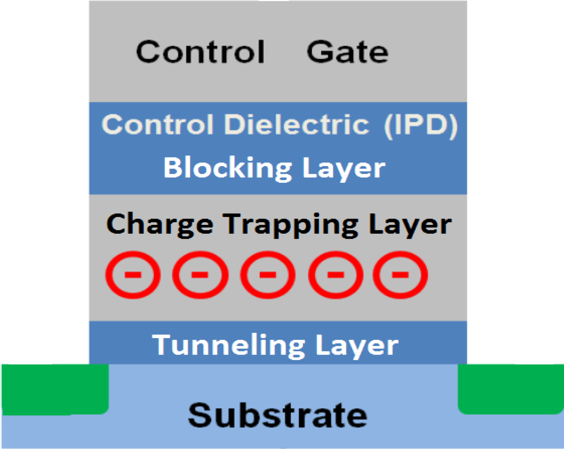
2. Background Knowledge


3. Recent Developments
3.1. Charge Trapping Layer


| High-k as CT Layer | Deposition Technique | Program/Erase Characteristic | Endurance Characteristics | Retention Characteristics | |
|---|---|---|---|---|---|
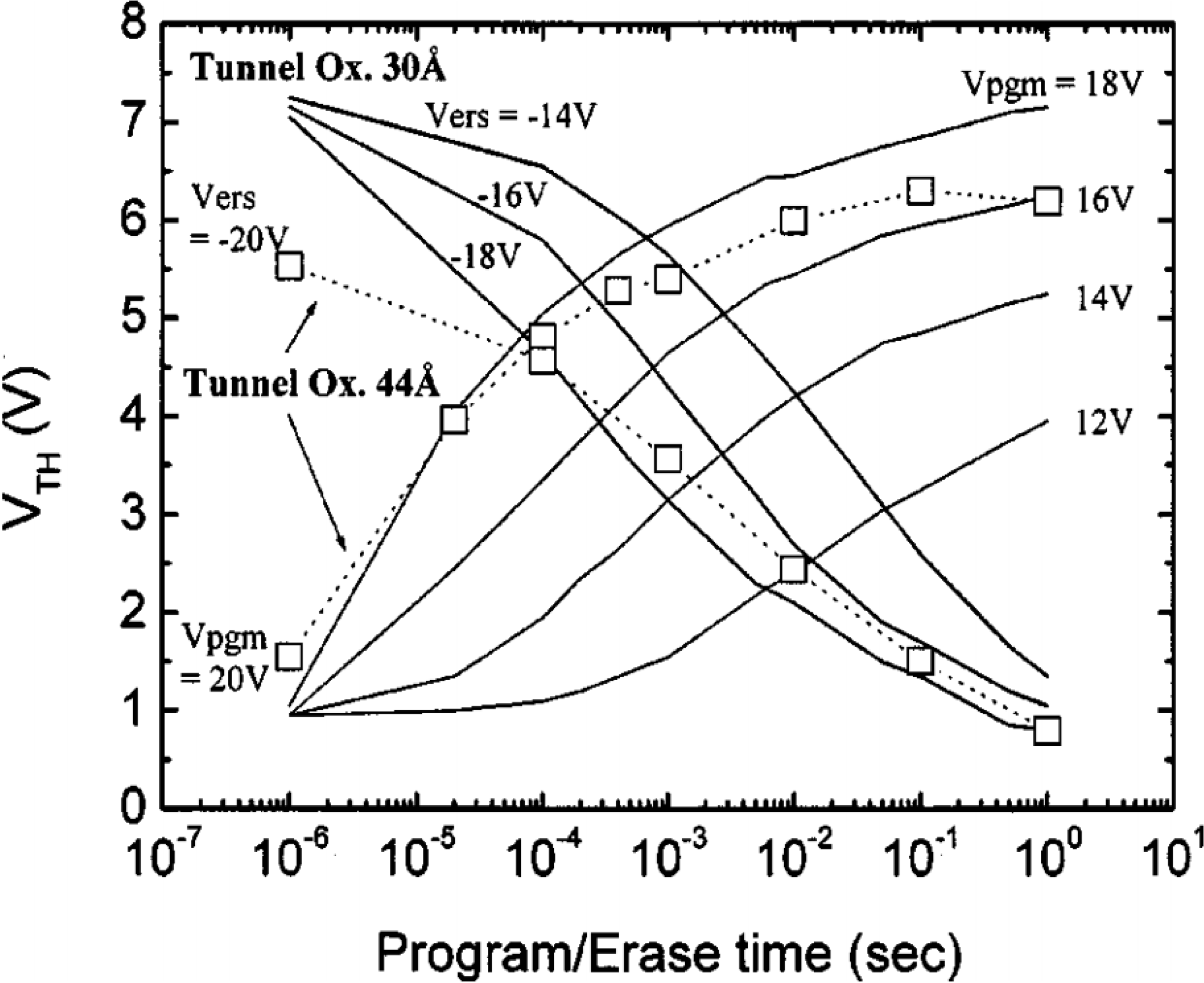
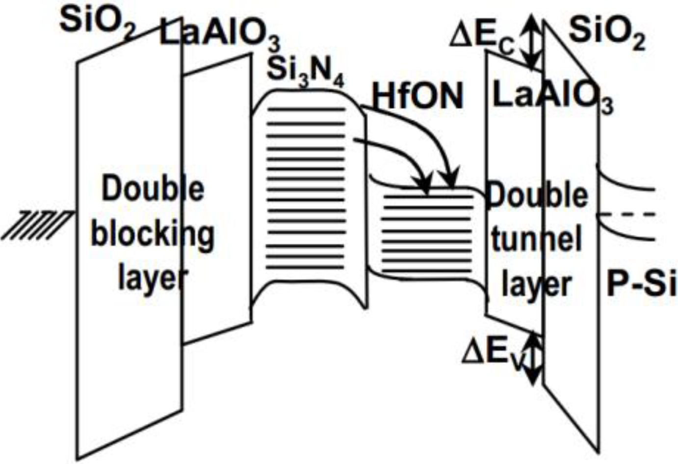
| Si3N4 + HfON | The layers of the TaN-[SiO2-LaAlO3]-[Si3N4-HfON]-[LaAlO3-SiO2]-Si devices comprised 2.5 nm of thermal SiO2, 2.5 nm of PVD LaAlO3, 5 nm of reactive PVD HfON0.2 and 5 nm of Si3N4 by LPCVD. Then 8 nm LaAlO3 by PVD, 5 nm SiO2 by PECVD, and 200 nm TaN by PVD. This was followed by standard gate definition, self-aligned P+ implantation and an RTA. | 150 °C and ± 16 V program/erase (P/E), the device showed P/E speed of 100 μs, an initial ΔVth window of 5.6 V. | a large 105-cycle window of 4.9 V and 103-cycled 10-year retention window of 4.1 V, at ±16 V 100 μs P/E. | An initial ΔVth window of 5.6 V is set and later extrapolated 10 year retention of 3.8 V. | |
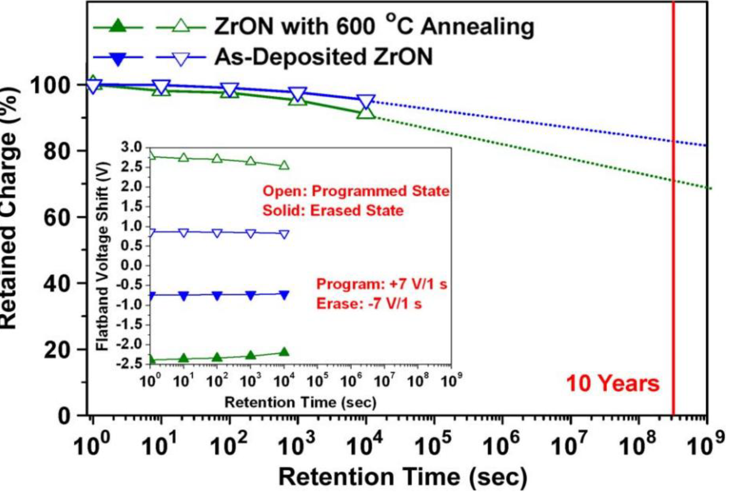
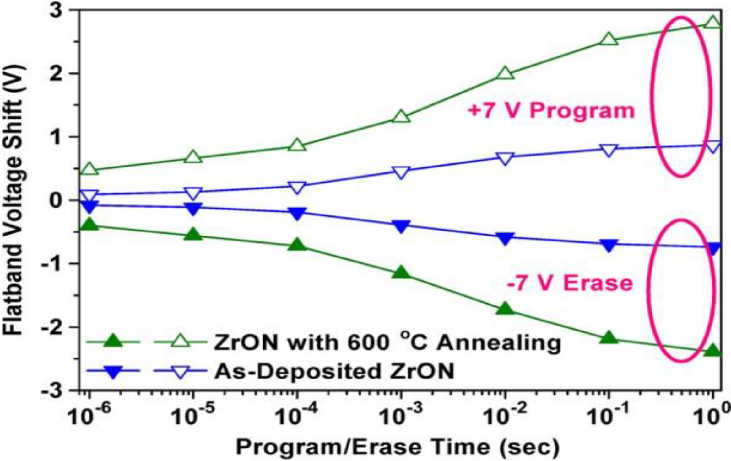
| ZrON | ZrON film was deposited in a reactive magnetron sputtering system as the charge-trapping layer. To form the ZrON film, a pure Zr target was sputtered in an oxygen (4-sccm)/nitrogen (12-sccm)/argon mixture (24-sccm) gas ambient. A subsequent annealing was performed on some as-deposited samples in a N2 ambient at 600 °C for 30 min. | 3.81 V hysteresis memory window by ±7 V P/E voltage and 1.98 V flat-band voltage shift by programming at +7 V for 10 ms. | negligible degradation of the memory window up to 105 P/E cycles from the endurance measurement, in which ±7 V with 10 ms gate pulse-width used. | 28.6% charge loss after ten-year operation at 85 °C. | |
| HfO2 | After a growth of thermal oxide with a thickness of 3 nm at 700 °C in dry O2 ambient, a deposition of HfO2 layers ranging from 8 to 2 nm was followed by atomic layered chemical vapor deposition method at 300 °C to evaluate the effect of thickness on the charge trapping and tunneling characteristics. | The memory window for 8 nm HfO2 layer is 1.5 V at high frequency of 1 MHz and sweep voltage of ±5 V. | insufficient data given. | An initial memory window of 6.16 V; after 10 years, the memory window of 4.26 V. Charge loss rate of 30.8%. | |
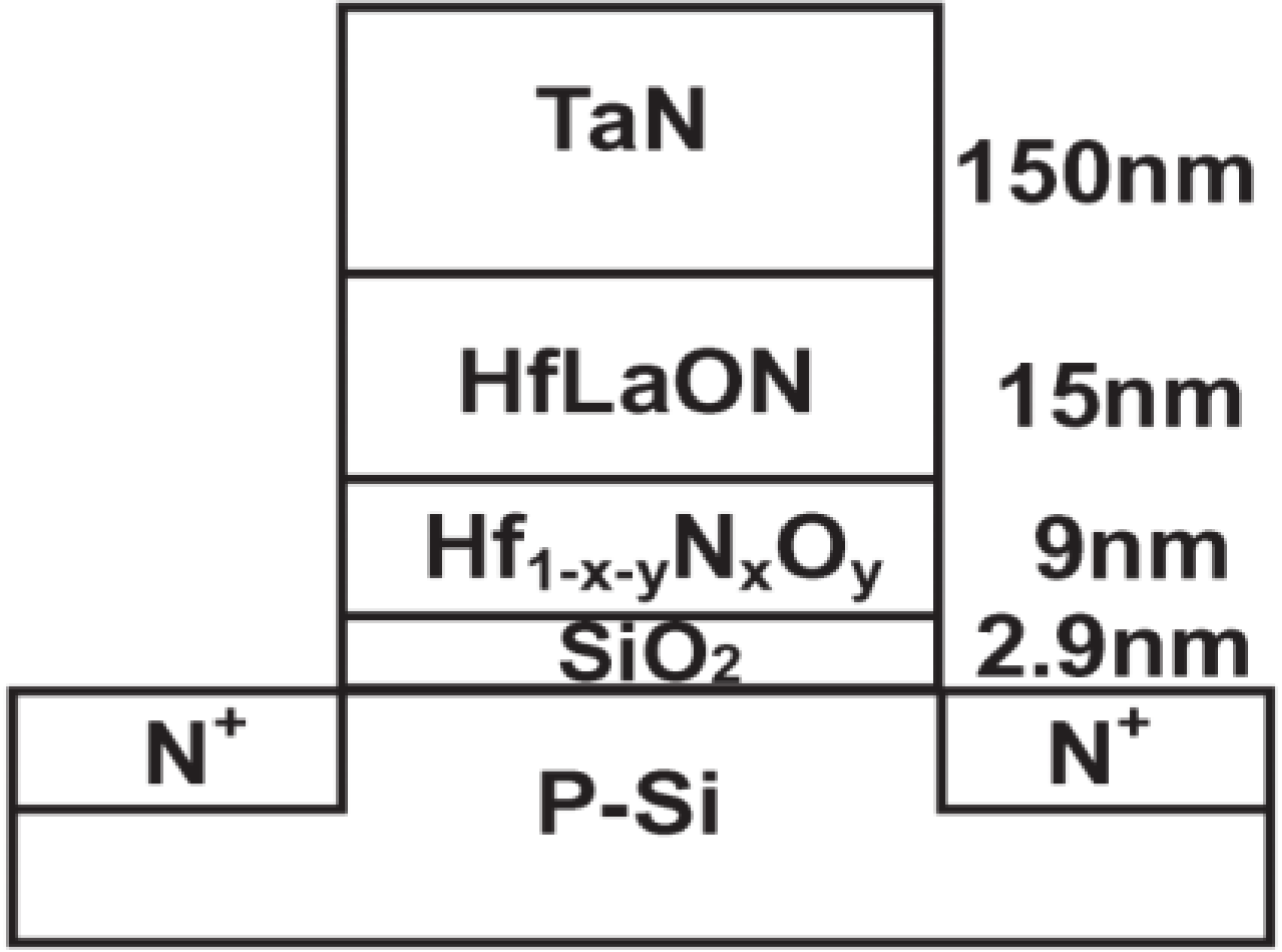
| Hf1−x−yNxOy | A 9-nm Hf1−x−yNxOy layer was deposited by reactive sputtering under a mixed O2 and N2 conditions with different O2/N2 ratios to study the N% dependence of the MONOS device integrity. | The Hf0.3N0.2O0.5 MONOS device showed ±9 V P/E voltage, 100 μs P/E speed, large initial 2.8 V memory window. | memory windows of 2.4 V and 1.7 V after 105 cycles at ±9 V 100 μs P/E for Hf0.3N0.2O0.5 devices and Hf0.35N0.10O0.55 MONOS devices, respectively. | a ten-year expected retention of 1.8 V at 85 °C or 1.5 V at 125 °C. | |
| HfAlO2 | For the SOHOS device, pure HfO2 and Al2O3 films were deposited by the ALD, while HfAlO films were deposited by metal organic chemical vapor deposition using a single cocktail source. The Al2O3 concentration in HfAlO was kept at 10%. | From the programming (Vg − Vfb = 6 V) and erasing (Vg − Vfb = −6 V), memory window is 3 V at 100 ms of P/E process. | HfAlO devices show a negligible degradation in the threshold voltage window after 104 W/E cycles. | The initial Vfb after programming is 3.5 V for 12.5 nm HfAlO and after 104 s the value retains at 3.4 V. | |
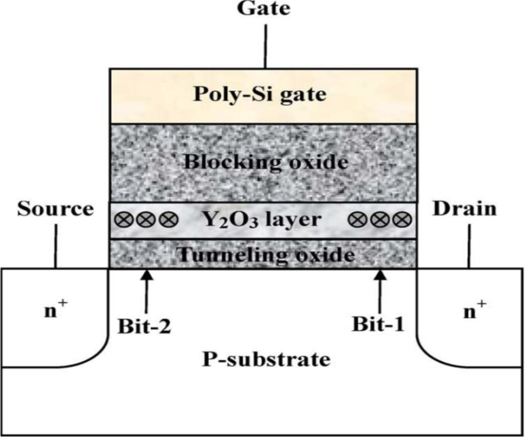
| Y2O3 | A 3 nm Y2O3 film was deposited on the tunneling oxide by sputtering with yttrium target in a system with a base pressure of 9.8 × 10⁻³ m·bar at room temperature. The sputtering process was performed in diluted O2(Ar/O2 = 25/5) ambient sputtering power of 100 W, at sputter rates of about 2.5 Å/min. Rapid thermal process anneal of 700 °C in N2,O2, or N2O ambient for 30 s was then performed to transform Y2O3 film into Y-silicate charge trapping layer. | For the condition of VD = 6 V and VG = 8 V at 1ms, a high-k Y2O3 SONOS-type memory after N2 annealing exhibits a larger memory window of 2.43 V compared with other annealing gases. | The values of Vth in the program and erase states for Y-silicate charge trapping layer memory prepared at a N2 gas annealing did not increase significantly up to 105 P/E cycles. | An yttrium silicate trapping storage layer memory annealed in N2 gas exhibits a small charge loss of about 4% measured time up to 104 s and at 25 °C. At the temperature at 125 °C, SONOS-type memory prepared under an Y2O3 trapping layer and annealed in N2 gas has a lower charge loss of 22% during the program state compared with other annealing gases. | |
| Tb2O3 | The 8 nm Tb2O3 film was deposited on the tunneling oxide by reactive sputtering in diluted O2 from a terbium target as a charge trapping layer. The wafers were annealed in O2 gas for 30 s at 800 °C by rapid thermal annealing. | Threshold voltage shifting (memory window of 1.41 V operated at Vg = 8 V at 0.1 s). | The values of VFB in the program and erase states did not increase significantly up to 105 P/E cycles. | Charge loss 10% measured time up to 104 s at 85 °C. | |
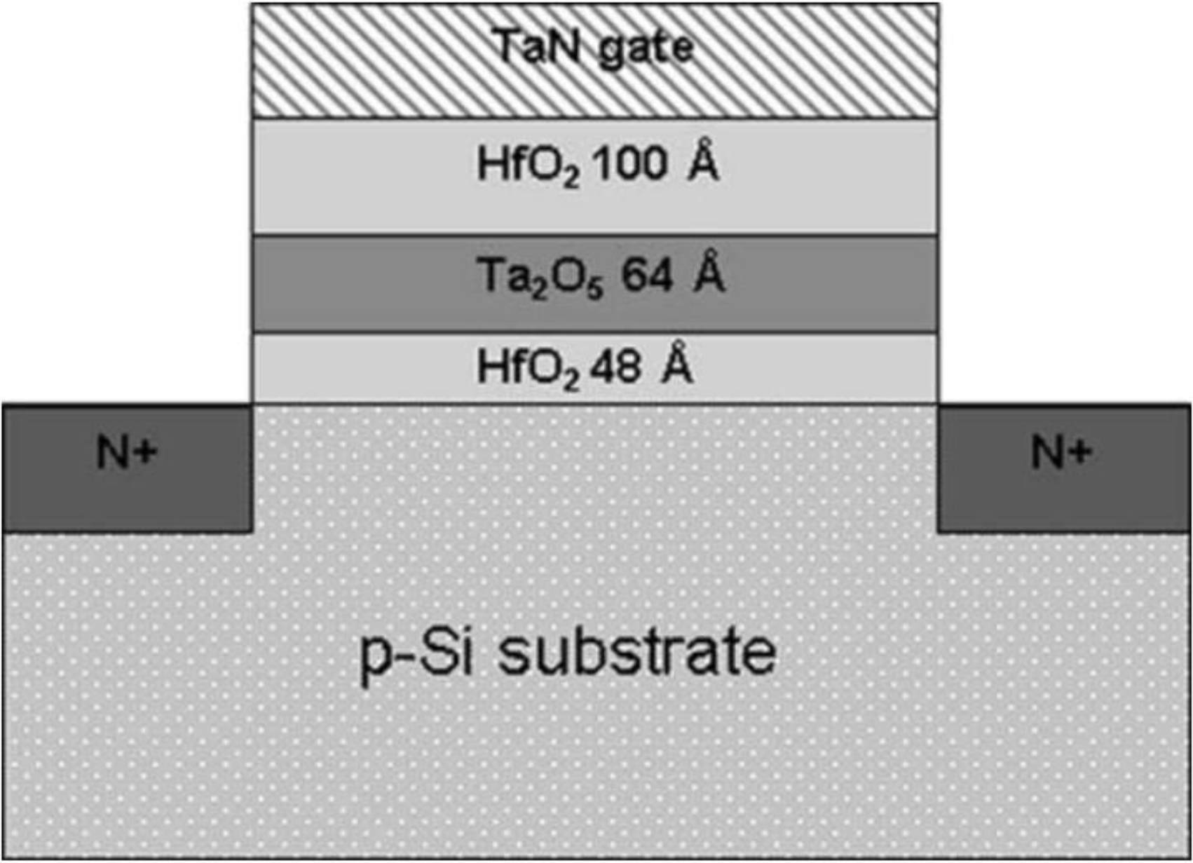
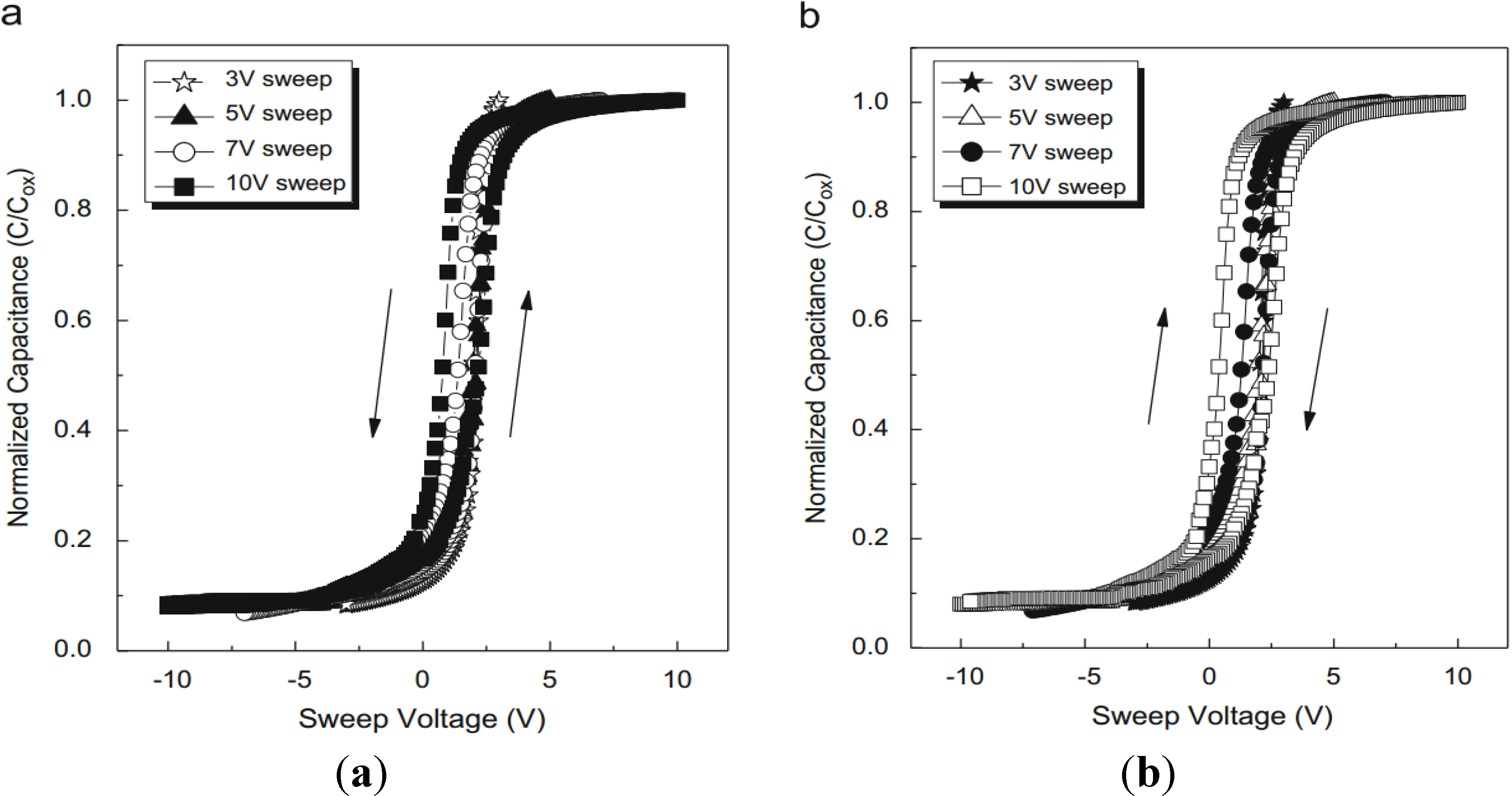
| Ta2O5 | After standard clean, the substrate was first annealed in NH3 at 700 °C, 10s to improve interface quality, followed by CVD HfO2 tunneling oxide layer formation using Hafnium t-butoxide (Hf(OC4H9)4 at 500 °C. The Ta2O5 charge-trapping layer was formed by oxidation of physical vapor deposition (PVD) Ta at 550 °C. | Memory windows of about 0.8V when the device is programmed with ±8 V-1-ms gate pulse; The device can be written starting from 10 us and erased from 1 ms for 6 and 7 V. | Memory window has no obvious shrink after 10 write/erase cycles with 8 V 1 ms stress at room temperature. | Retention characteristics at room temperature and 85 °C demonstrate a decay rate of 50 mV/dec. Memory window extrapolated at ten years is 0.64 V (initial 0.8 V) at room temperature, and 0.42 V at 85 °C. | |
| MoOx | The embedded MoOx layer was sputtered from the Mo target in Ar/O2(1:1) at 5 mTorr and 100 W for 15 s. The as-deposited MoOx layer was transformed into nanocrystalline MoO3, after the PDA step at 800 °C for 1 min in the pure N2 ambient by rapid thermal annealing. | The nc-MoOx sample shows a large VFB shift of −0.52 V after the −8 V stress, which corresponds to the hole trapping density of 1.14 × 1012 cm−2. On the other hand, for the same sample, a very small positive VFB shift, i.e., 0.04 V is observed after the +8 V stress. | insufficient data given. | About 54% of trapped holes (under the −8 V stress condition) remain in the sample after 10 years. Also, about 52% of trapped holes (under the −7 V stress condition) remain in the sample after 10 years. | |
| SrTiO3 | 3 nm SrTiO3 was deposited on the SiO2 by reactive sputtering using a SrTiO3 target in a mixed Ar/N2 (4/1) or Ar/O2 (4/1) ambient. | memory window (8.4 V at ±10 V sweeping voltage), P/E speeds (1.8 V at 1 ms +8 V). | memory window after 105 cycles is 2.13 V compared with initial value of 2.07 V. | charge loss of 38% after 104 s. | |
| BaTiO3 | 10 nm Zr-doped BaTiO3 was deposited on the SiO2 by reactive sputtering using BaTiO3 and Zr targets in a mixed Ar/O2 ambient, and the atomic ratio of Zr and Ti was determined to be 1/3. The sample went through PDA in a N2 ambient at 900 °C for 30 s. | memory window (8.3 V at ±12 V for 1 s), but higher program speed at low gate voltage (3.2 V at 100 μs +6 V). | Under a ±12 V 100 μs stress pulse the P/E windows of the Zr-BTO sample before and after the 105-cycle stressing are 6.4 and 6.6 V, respectively, and negligible degradation happens. | charge loss of 6.4% at 150 °C for 104 s. | |
| Al2O3 + La2O3 + Al2O3 | Al2O3/La2O3/Al2O3 films were deposited on (100) ntype Si wafers (SILTRON, Korea) by a MOCVD system. N2 was used as a carrier gas for La and Al precursor. | maximum memory window of this film of about 1.12 V was observed at 11 V for 10 ms in the program mode and at −13 V for 100 ms in the erase mode. | memory window after 104 cycles is 1.2 V compared with initial value of 1.12 V. | insufficient data given. | |
| Si3N4 + Al2O3 + HfO2 | Si3N4 was deposited by low-pressure chemical vapor deposition, and Al2O3 and HfO2 were deposited using the metal–organic chemical vapor deposition method. High-temperature annealing was performed on all samples in a N2 ambient for 30 s at 900 °C by rapid thermal anneal. | at VP = 16 V and VE = −16 V for 1 s, memory window of this film of about 10 V, P/E speeds (6.1 V at 1 ms +8 V). | no sufficient data given. | charge loss of 4% after 104 s. |
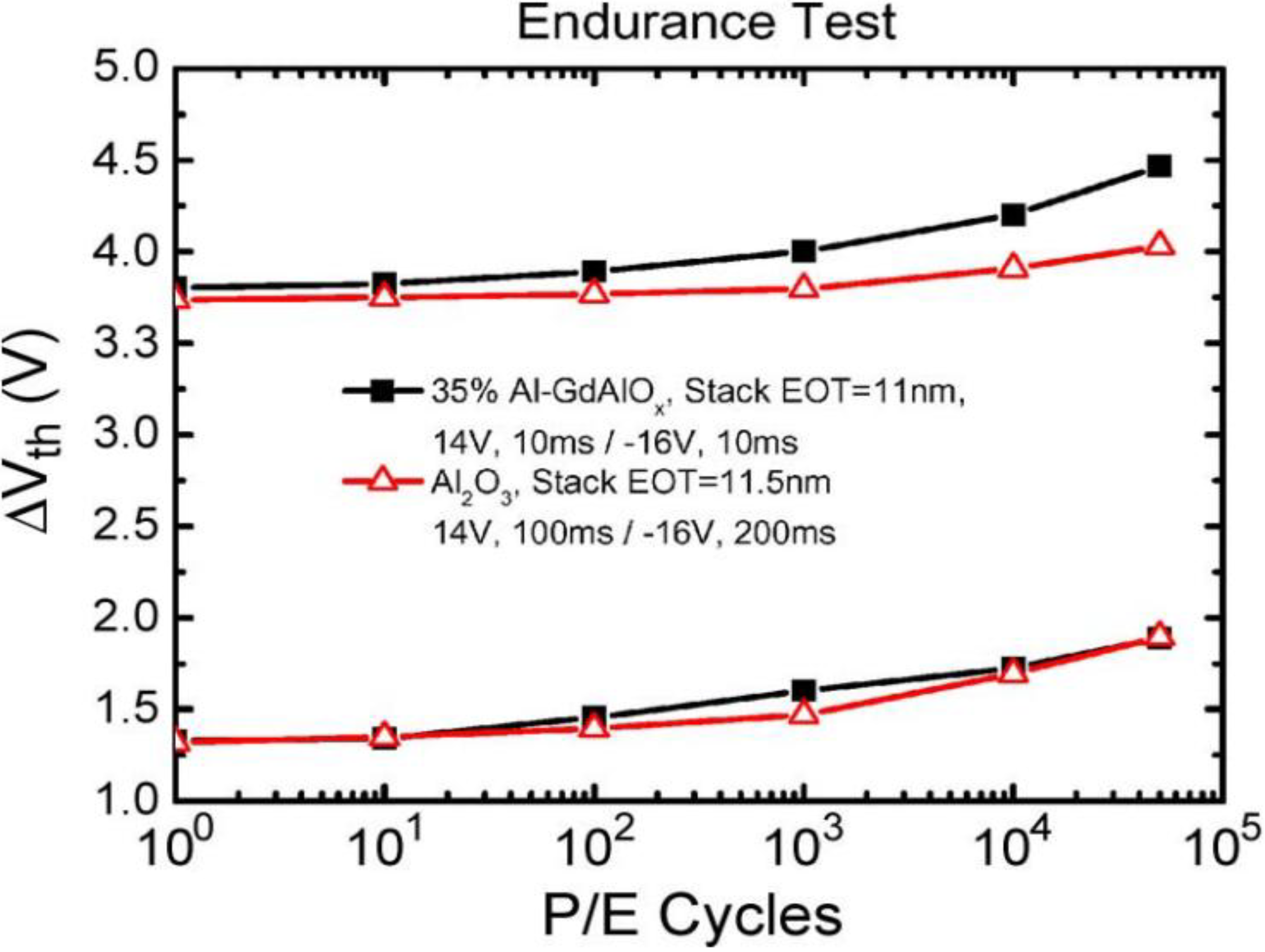
3.2. Blocking Layer
3.3. Tunneling Layer


| Channel Hot Electron (CHE) | Fowler-Nordheim (F-N) | |
|---|---|---|
| Advantages | The physical mechanism of CHE is relatively simple to understand qualitatively. An electron traveling from the source to the drain gains energy from the lateral electric field and loses energy to the lattice vibrations.
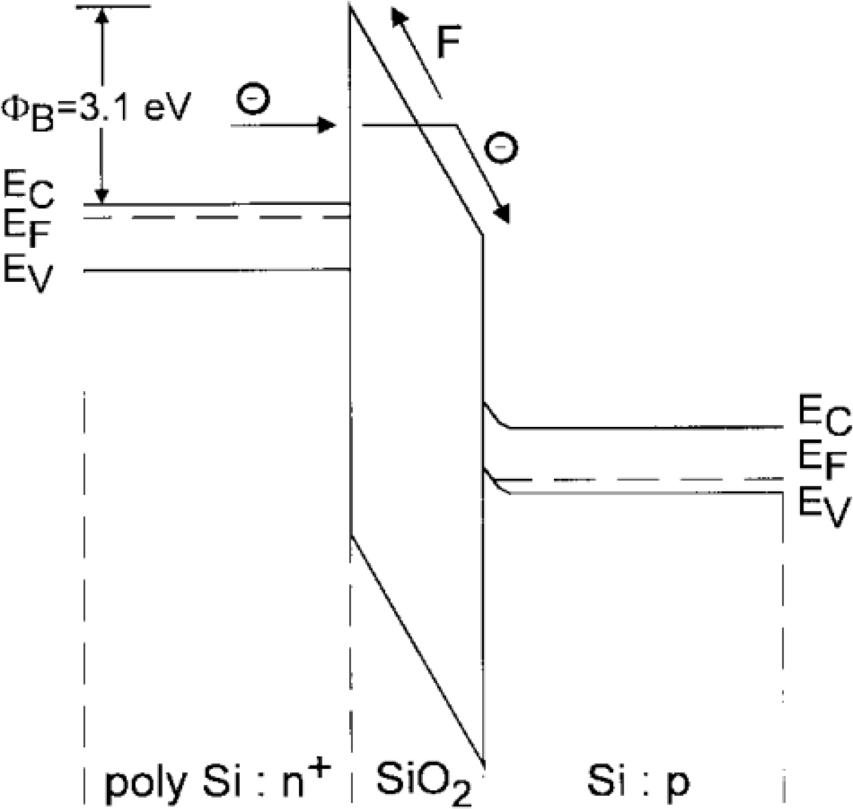
At low fields, this is a dynamic equilibrium condition, which holds until the field strength reaches approximately 100 kV/cm. For fields exceeding this value, electrons are no longer in equilibrium with the lattice, and their energy relative to the conduction band edge begins to increase. A lateral electric field (between source and drain) “heats” the electrons and a transversal electric field (between channel and control gate) injects the carriers through the oxide. The programming speed of CHE for conventional floating gate memory is faster. | The F-N mechanism is widely used in NVM, particularly in EEPROM. With a relatively thick oxide (20–30 nm) one must apply a high voltage (20–30 V) to have an appreciable tunnel current. With thin oxides, the same current can be obtained by applying a much lower voltage. An optimum thickness is chosen in present devices, which use the tunneling phenomenon to tradeoff between performance constraints (programming speed, power consumption, etc.) and reliability concerns. There are three main reasons for this choice:
|
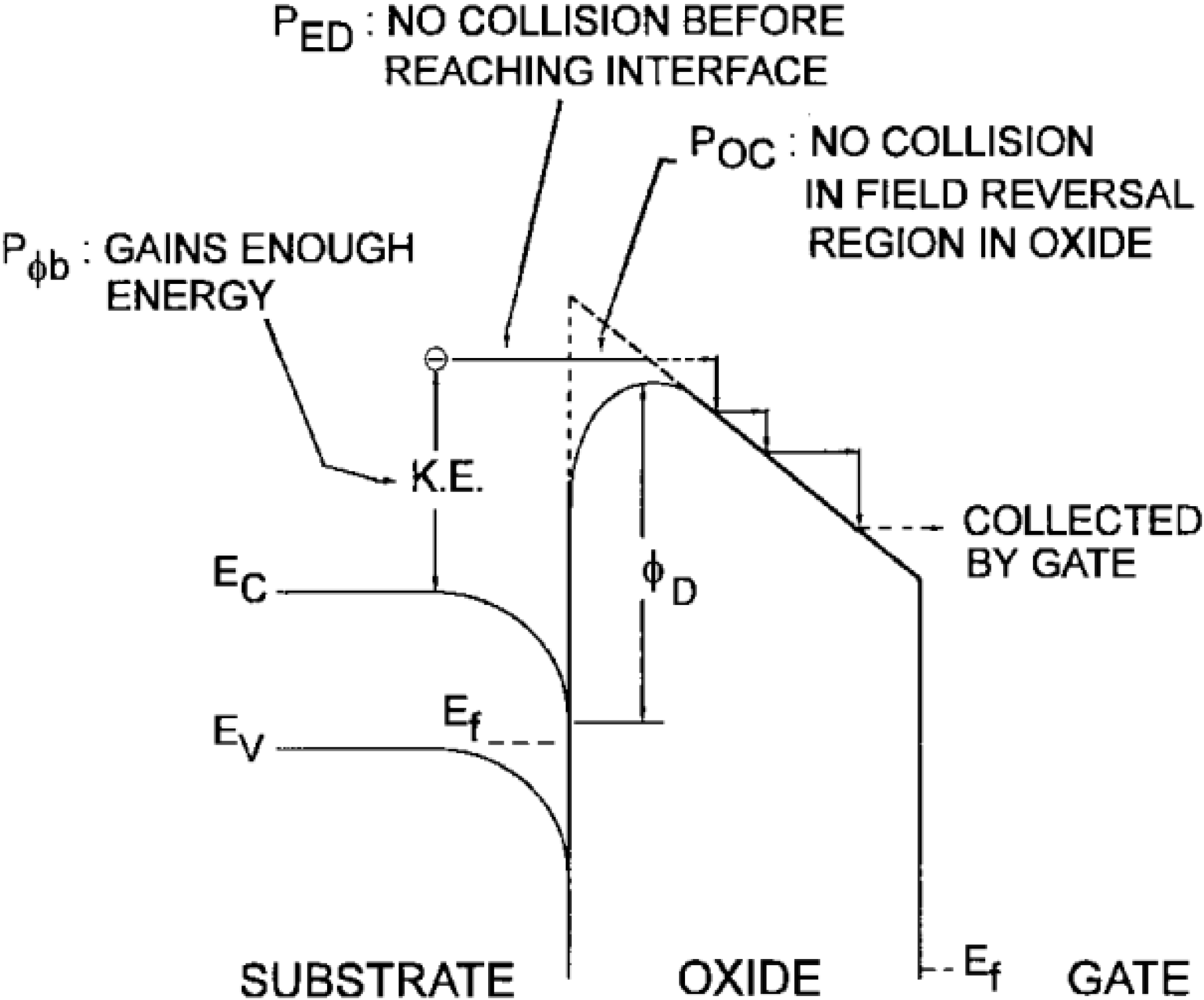
| Disadvantages | The probability of the injecting electrons is quite low and hot electron injection is an inefficient method of programming. For an electron to overcome the potential barrier, three requirements must be meet accordingly:
| The exponential dependence of tunnel current on the oxide-electric field causes some critical problems of process control because. Very small variation of oxide thickness among the cells in a memory array produces a great difference in programming or erasing currents.
Bad quality oxides are rich of interface and bulk traps, and trap-assisted tunneling is made possible since the equivalent barrier height seen by electrons is reduced and tunneling requires a much lower oxide field than 10 MV/cm. The oxide defects must be avoided to control program/erase characteristics and to have good reliability. Frequent program and erase operations induce an increase of trapped charge in the oxide. This affects the barrier height, which is lower in the case of positive and higher in the case of negative trapping, respectively, thus increasing or decreasing the tunnel currents. |
4. Conclusions
Acknowledgments
Author Contributions
Conflicts of Interest
References
- She, M.; King, T.-J.; Hu, C.M.; Zhu, W.J.; Luo, Z.J.; Han, J.-P.; Ma, T.-P. JVD silicon nitride as tunnel dielectric in p-channel flash memory. IEEE Electron Device Lett. 2002, 23, 91–93. [Google Scholar] [CrossRef]
- Ma, T.P.; Han, J.P. Why is nonvolatile ferroelectric memory field-effect transistor still elusive? IEEE Electron Device Lett. 2002, 23, 386–388. [Google Scholar] [CrossRef]
- Lee, C.H.; Park, K.C.; Kim, K. Charge-trapping memory cell of SiO2/SiN/high-k dielectric Al2O3 with TaN metal gate for suppressing backward-tunneling effect. Appl. Phys. Lett. 2005, 87, 073510:1–073510:3. [Google Scholar]
- Zhang, G.; Wang, L.-K.; Won, J.Y.; Li, M.-F. Spatial distribution of charge traps in a SONOS-type flash memory using a high-k trapping layer. IEEE Trans. Electron Devices 2007, 54, 3317–3324. [Google Scholar] [CrossRef]
- Yoshimitsu, Y.; Yoshinari, K.; Toshimasa, M. Scalable Virtual-Ground Multilevel-Cell Floating-Gate Flash Memory. IEEE Trans. Electron Devices 2013, 60, 2518–2524. [Google Scholar] [CrossRef]
- Lu, C.-Y.; Hsieh, K.-Y.; Liu, R. Future challenges of flash memory technologies. Microelectron. Eng. 2009, 86, 283–286. [Google Scholar]
- Zhao, C.Z.; Zhang, J.F.; Zahid, M.B.; Groeseneken, G.; Degraeve, R.; de Gendt, S. Impact of gate materials on positive charge formation in HfO2/SiO2 stacks. Appl. Phys. Lett. 2006, 89, 023507:1–023507:3. [Google Scholar]
- Ishiwara, H. Current status of ferroelectric-gate Si transistors and challenge to ferroelectric-gate CNT transistors. Curr. Appl. Phys. 2009, 9, S2–S6. [Google Scholar] [CrossRef]
- Fitsilis, M.; Mustafa, Y.; Waser, R. Scaling the ferroelectric field effect transistor. Integr. Ferroelectr. Int. J. 2005, 70, 29–44. [Google Scholar] [CrossRef]
- Rueckes, T.; Kim, K.; Joselevich, E.; Tseng, G.Y.; Cheung, C.-L.; Lieber, C.M. Carbon nanotube-based nonvolatile random access memory for molecular computing. Science 2000, 289, 94–97. [Google Scholar] [CrossRef]
- Choi, W.Y.; Osabe, T.; Liu, T.-S. Nano-electro-mechanical nonvolatile memory (NEMory) cell design and scaling. IEEE Trans. Electron Devices 2008, 55, 3482–3488. [Google Scholar] [CrossRef]
- Kryder, M.H.; Kim, C.S. After hard drives—What comes next? IEEE Trans. Magn. 2009, 45, 3406–3413. [Google Scholar] [CrossRef]
- Pagnia, H.; Sotnik, N. Bistable switching in electroformed metal-insulator-metal devices. Phys. Status Solidi 1988, 108, 11–65. [Google Scholar] [CrossRef]
- Jung, Y.; Yang, C.Y.; Lee, S.H.; Agarwal, R. Phase-change Ge-Sb nanowires: Synthesis, memory switching, and phase-instability. Nano Lett. 2009, 9, 2103–2108. [Google Scholar] [CrossRef]
- Waser, R.; Aono, M. Nanoionics-based resistive switching memories. Nat. Mater. 2007, 6, 833–840. [Google Scholar] [CrossRef]
- Scott, J.C.; Bozano, L.D. Nonvolatile memory elements based on organic materials. Adv. Mater. 2007, 19, 1452–1463. [Google Scholar] [CrossRef]
- Brewer, J.; Gill, M. Nonvolatile Memory Technologies with Emphasis on Flash: A Comprehensive Guide to Understanding and Using NVSM Devices; IEEE Press: Piscataway, NJ, USA, 2008. [Google Scholar]
- International Technology Roadmap for Semiconductors: Process Integration, Devices and Structures. 2009. Available online: http://www.itrs.net/Links/2009ITRS/Home2009.htm (accessed on 14 July 2014).
- De Salvo, B. Silicon Non-Volatile Memories: Paths of Innovation; John Wiley & Sons: Hoboken, NJ, USA, 2010. [Google Scholar]
- Zhao, Y. Design of higher-k and more stable rare earth oxides as gate dielectrics for advanced CMOS devices. Materials 2012, 5, 1413–1438. [Google Scholar] [CrossRef]
- Tao, J.; Zhao, C.Z.; Zhao, C.; Taechakumput, P.; Werner, M.; Taylor, S.; Chalker, P.R. Extrinsic and intrinsic frequency dispersion of high-k materials in Capacitance-Voltage measurements. Materials 2012, 5, 1005–1032. [Google Scholar] [CrossRef]
- Suzuki, M. Comprehensive study of lanthanum aluminate high-dielectric-constant gate oxides for advanced CMOS devices. Materials 2012, 5, 443–477. [Google Scholar] [CrossRef]
- Miyata, N. Study of direct-contact HfO2/Si Interfaces. Materials 2012, 5, 512–527. [Google Scholar] [CrossRef]
- Zhao, C.; Zhao, C.Z.; Werner, M.; Taylor, S.; Chalker, P.R. Dielectric relaxation of high-k oxides. Nanoscale Res. Lett. 2013, 8, 1–12. [Google Scholar] [CrossRef]
- Zhao, C.; Zhao, C.Z.; Werner, M.; Taylor, S.; Chalker, P.R.; King, P. Grain size dependence of dielectric relaxation in cerium oxide as high-k layer. Nanoscale Res. Lett. 2013, 8. [Google Scholar] [CrossRef]
- Zhao, C.; Zhao, C.Z.; Tao, J.; Werner, M.; Taylor, S.; Chalker, P.R. Dielectric relaxation of lanthanide-based ternary oxides: Physical and mathematical models. J. Nanomater. 2012, 2012. [Google Scholar] [CrossRef]
- Zhao, C.; Zhao, C.Z.; Werner, M.; Taylor, S.; Chalker, P.R. Advanced CMOS gate stack: Present research progress. ISRN Nanotechnol. 2012, 2012. [Google Scholar] [CrossRef]
- Zhao, C.Z.; Werner, M.; Taylor, S.; Chalker, P.R.; Jones, A.C.; Zhao, C. Dielectric aelaxation of la-doped zirconia caused by annealing ambient. Nanoscale Res. Lett. 2011, 6. [Google Scholar] [CrossRef]
- Dai, M.-K.; Lin, T.-Y.; Yang, M.-H.; Lee, C.-K.; Huang, C.-C.; Chen, Y.-F. High-performance organic nano-floating-gate memory devices based on graphite nanocrystals as charge-trapping elements and high-k Ta2O5 as a controlled gate dielectric. J. Mater. Chem. C 2014, 2, 5342–5349. [Google Scholar]
- Cao, Z.-Y.; Li, A.-D.; Li, X.; Cao, Y.-Q.; Wu, D. Ti–Al–O nanocrystal charge trapping memory cells fabricated by atomic layer deposition. Thin Solid Films 2014, 563, 6–9. [Google Scholar] [CrossRef]
- Ozaki, S.; Kato, T.; Kawae, T.; Morimoto, A. Influences of low-temperature postdeposition annealing on memory properties of Al/Al2O3/Al-rich Al-O/SiO2/p-Si charge trapping flash memory structures. J. Vac. Sci. Technol. B 2014, 32, 031213:1–031213:5. [Google Scholar]
- Zhu, H.; Bonevich, J.E.; Li, H.; Richter, C.A.; Yuan, H.; Kirilov, O.; Li, Q. Discrete charge states in nanowire flash memory with multiple Ta2O5 charge-trapping stacks. Appl. Phys. Lett. 2014, 104. [Google Scholar] [CrossRef]
- Leong, W.L.; Mathews, N.; Tan, B.; Vaidyanathan, S.; Dotz, F.; Mhaisalker, S. Towards printable organic thin film transistor based flash memory devices. J. Mater. Chem. 2011, 21, 5203–5214. [Google Scholar]
- Pavan, P.; Bez, R.; Olivo, P.; Zanoni, E. Flash Memory Cells—An Overview. Proc. IEEE 1997, 85, 1248–1271. [Google Scholar] [CrossRef]
- Keenney, S.; Bez, R.; Cantarelli, D.; Piccinini, F.; Mathewson, A.; Lombardi, C. Complete transient simulation of Flash EEPROM devices. IEEE Trans. Electron Devices 1992, 39, 2750–2757. [Google Scholar] [CrossRef]
- Bez, R.; Camerlenghi, E.; Modelli, A.; Visconti, A. Introduction to FLASH memory. Proc. IEEE 2003, 91, 489–502. [Google Scholar] [CrossRef]
- Wu, Y.H.; Chen, L.L.; Wu, J.R.; Wu, M.L.; Lin, C.C.; Chang, C.H. Nonvolatile memory with nitrogen-stabilized cubic-phase ZrO2 as charge-trapping layer. IEEE Electron Device Lett. 2010, 31, 1008–1010. [Google Scholar]
- White, M.H.; Adams, D.A.; Bu, J. On the go with SONOS. IEEE Circuits Devices Mag. 2000, 16, 22–31. [Google Scholar] [CrossRef]
- Lin, S.H.; Chin, A.; Yeh, F.S.; McAlister, S.P. Good 150 °C retention and fast erase charge-crapping-engineered memory with scaled Si3N4. In proceedings of IEEE International Electron Devices Meeting, San Francisco, CA, USA, 15–17 December 2008; pp. 1–4.
- You, H.-W.; Cho, W.-J. Charge trapping properties of the HfO2 layer with various thicknesses for charge trap flash memory applications. Appl. Phys. Lett. 2010, 96, 093506:1–093506:3. [Google Scholar]
- Yang, H.J.; Cheng, C.F.; Chen, W.B.; Lin, S.H.; Yeh, F.S.; McAlister, S.P.; Chin, A. Comparison of MONOS memory device integrity when using Hf1−x−yNxOy trapping layers with different N compositions. IEEE Trans. Electron Devices 2008, 55, 1417–1423. [Google Scholar] [CrossRef]
- Tan, Y.N.; Chim, W.K.; Choi, W.K.; Joo, M.S.; Byung, J.C. Hafnium aluminum oxide as charge storage and blocking-oxide layers in SONOS type nonvolatile memory for high-speed operation. IEEE Trans. Electron Devices 2006, 53, 654–662. [Google Scholar]
- Pan, T.-M.; Yeh, W.-W. High-performance high-k Y2O3 SONOS-type flash memory. IEEE Trans. Electron Devices 2008, 55, 2354–2360. [Google Scholar] [CrossRef]
- Pan, T.-M.; Jung, J.-S.; Chen, F.-H. Metal-oxide-high-k-oxide-silicon memory structure incorporating a Tb2O3 charge trapping layer. Appl. Phys. Lett. 2010, 97, 012906:1–012906:3. [Google Scholar]
- Wang, X.; Liu, J.; Bai, W.; Kwong, D.-L. A novel MONOS-type nonvolatile memory using high-k dielectrics for improved data retention and programming speed. IEEE Trans. Electron Devices 2004, 51, 597–602. [Google Scholar] [CrossRef]
- Liu, X.; Yang, C.H.; Kuo, Y.; Yuan, T. Nanocrystalline MoOx Embedded ZrHfO High k Memories Charge Trapping and Retention Characteristics. ECS Trans. 2012, 45, 203–209. [Google Scholar]
- Huang, X.D.; Lai, P.T.; Liu, L.; Xu, J.P. Nitrided SrTiO3 as charge-trapping layer for nonvolatile memory applications. Appl. Phys. Lett. 2011, 98. [Google Scholar] [CrossRef] [Green Version]
- Huang, X.D.; Sin, J.K.O.; Lai, P.T. Improved Charge-Trapping Characteristics of BaTiO3 by Zr Doping for Nonvolatile Memory Applications. IEEE Electron Device Lett. 2013, 34, 499–501. [Google Scholar] [CrossRef] [Green Version]
- Kim, J.H.; Cha, S.Y.; Choi, D.J. Memory characteristics of Al2O3/La2O3/Al2O3 multi-layer films with various blocking and tunnel oxide thicknesses. Mater. Sci. Semicond. Process. 2010, 13, 9–12. [Google Scholar] [CrossRef]
- Ye, Z.H.; Chang-liao, K.S.; Tsai, C.Y.; Tsai, T.T.; Wang, T.K. Enhanced Operation in Charge-Trapping Nonvolatile Memory Device With Si3N4/Al2O3/HfO2 Charge-Trapping Layer. IEEE Electron Device Lett. 2012, 33, 1351–1353. [Google Scholar] [CrossRef]
- Lee, C.H.; Hur, S.H.; Shin, Y.C.; Choi, J.H.; Park, D.G.; Kim, K. Charge trapping device structure of SiO2/SiN/high-k dielectric Al2O3 for high-density flash memory. Appl. Phys. Lett. 2005, 86. [Google Scholar] [CrossRef]
- Pu, J.; Chan, D.S.; Kim, S.-J.; Cho, B.J. Aluminum-doped gadolinium oxides as blocking layer for improved charge retention in charge-trap-type nonvolatile memory devices. IEEE Trans. Electron Devices 2009, 56, 2739–2745. [Google Scholar] [CrossRef]
- He, W.; Pu, J.; Chan, D.S.; Cho, B.J. Performance improvement in charge-trap flash memory using lanthanum-based high-k blocking oxide. IEEE Trans. Electron Devices 2009, 56, 2746–2751. [Google Scholar]
- Huang, X.D.; Liu, L.; Xu, J.P.; Lai, P.T. Improved performance of yttrium-doped Al2O3 as inter-poly dielectric for flash-memory applications. IEEE Trans. Device Mater. Rel. 2011, 13, 490–494. [Google Scholar]
- Lue, H.-T.; Wang, S.-Y.; Lai, E.-K.; Shih, Y.-H.; Lai, S.-C.; Yang, L.-W.; Chen, K.-C.; Ku, J.; Hsieh, K.-Y.; Liu, R.; et al. BE-SONOS: A bandgap engineered SONOS with excellent performance and reliability. In Proceedings of IEEE International IEDM Technical Digest Electron Devices Meeting, Washington, DC, USA, 5 December 2005; pp. 547–550.
- Govoreanu, B.; Blomme, P.; Rosmeulen, M.; van Houdt, J.; de Meyer, K. VARIOT: A novel multilayer tunnel barrier concept for low voltage nonvolatile memory devices. IEEE Electron Device Lett. 2003, 24, 99–101. [Google Scholar]
© 2014 by the authors; licensee MDPI, Basel, Switzerland. This article is an open access article distributed under the terms and conditions of the Creative Commons Attribution license (http://creativecommons.org/licenses/by/3.0/).
Share and Cite
Zhao, C.; Zhao, C.Z.; Taylor, S.; Chalker, P.R. Review on Non-Volatile Memory with High-k Dielectrics: Flash for Generation Beyond 32 nm. Materials 2014, 7, 5117-5145. https://doi.org/10.3390/ma7075117
Zhao C, Zhao CZ, Taylor S, Chalker PR. Review on Non-Volatile Memory with High-k Dielectrics: Flash for Generation Beyond 32 nm. Materials. 2014; 7(7):5117-5145. https://doi.org/10.3390/ma7075117
Chicago/Turabian StyleZhao, Chun, Ce Zhou Zhao, Stephen Taylor, and Paul R. Chalker. 2014. "Review on Non-Volatile Memory with High-k Dielectrics: Flash for Generation Beyond 32 nm" Materials 7, no. 7: 5117-5145. https://doi.org/10.3390/ma7075117