Influence of Carrier Gas Composition on the Stress of Al2O3 Coatings Prepared by the Aerosol Deposition Method


Abstract
:1. Introduction
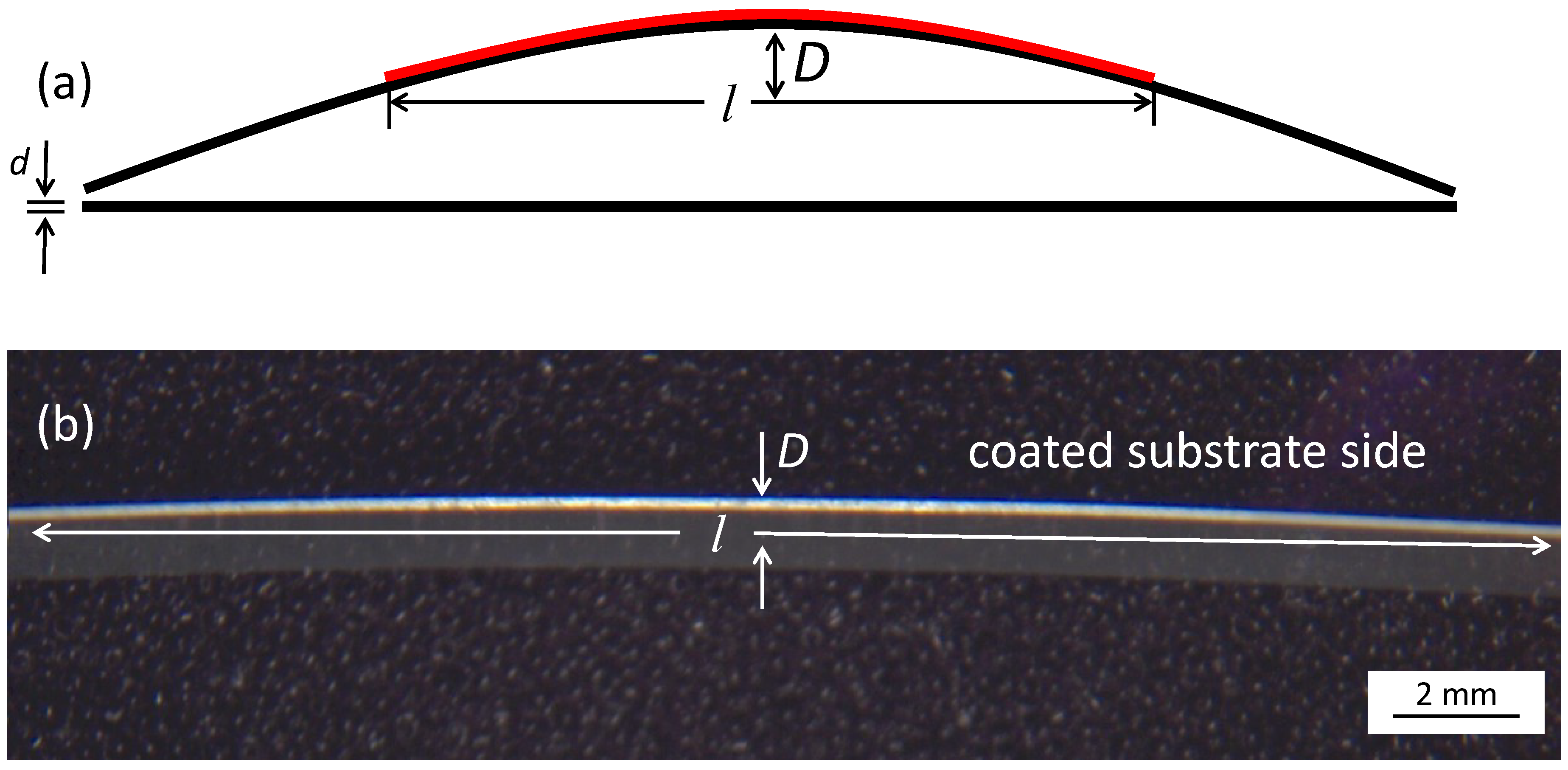
2. Experimental


| Parameters | Values |
|---|---|
| Orifice size of the nozzle | 10 × 0.5 mm2 |
| Distance nozzle—substrate | 3 mm |
| Substrate temperature | Room temperature |
| Gas flow rate | 6 L/min |
| Carrier gas | O2, N2, He, and mixtures as indicated in the experiments |
| Sweep rate | 1 mm/s |

3. Results and Discussion
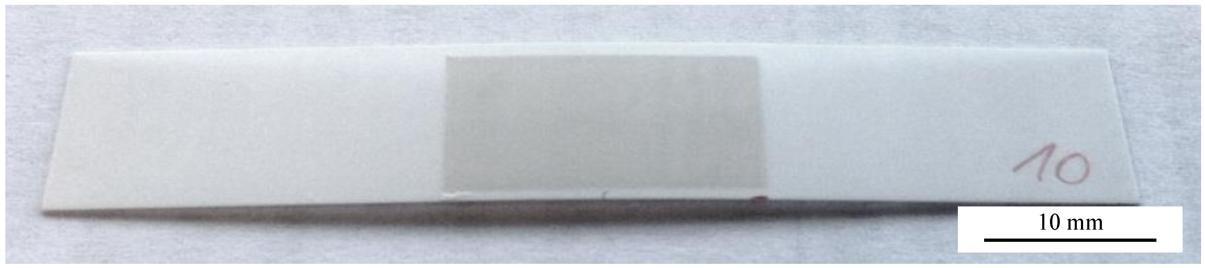
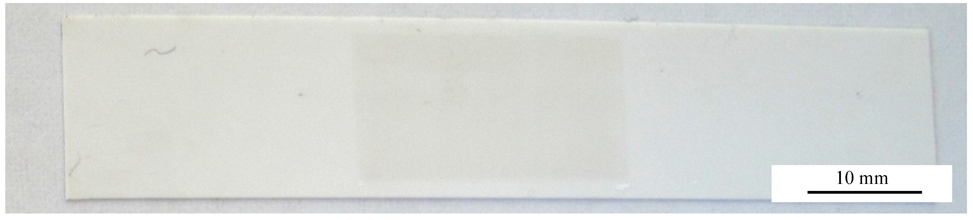
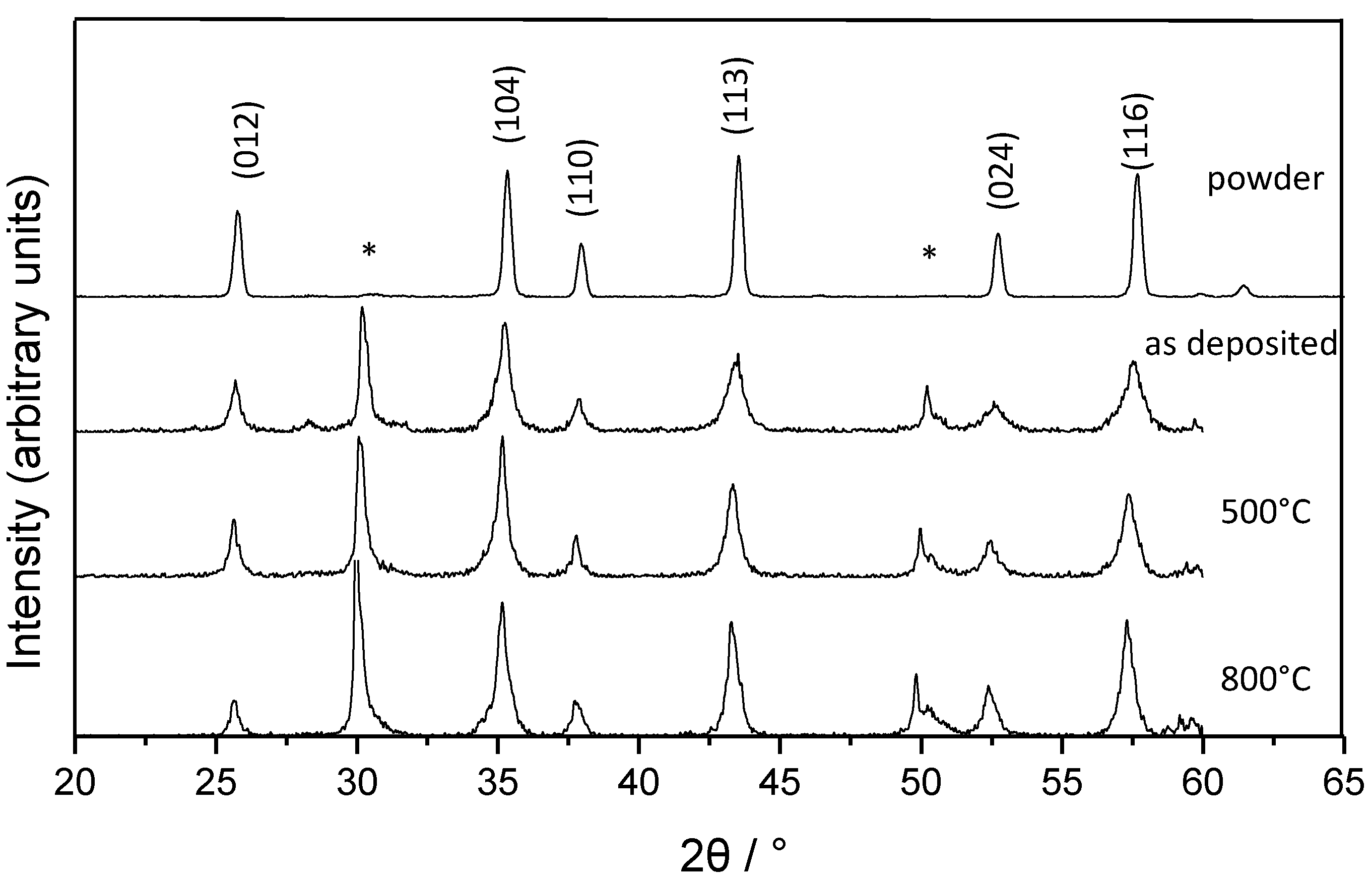
3.1. Characterization of the Deposited Films


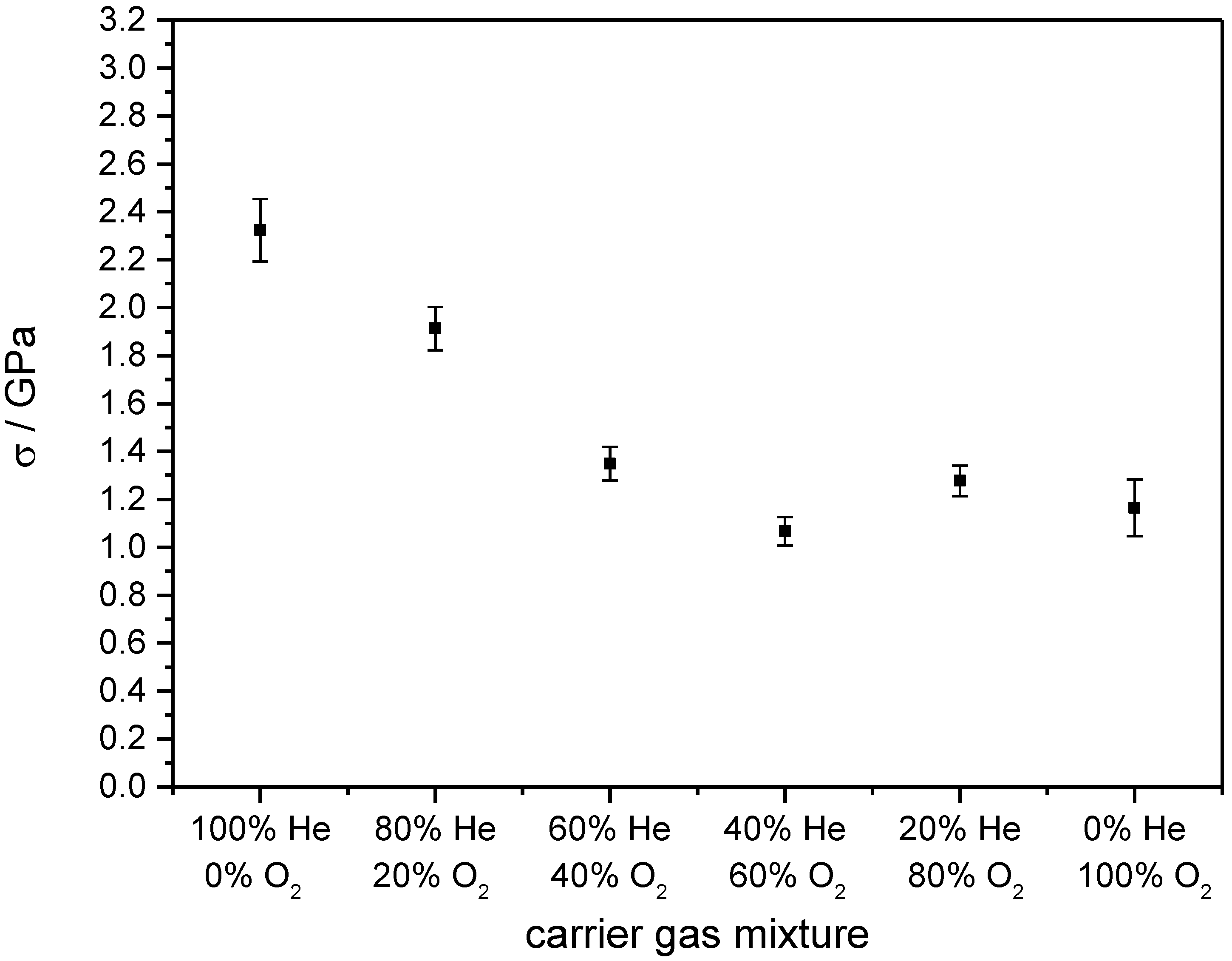
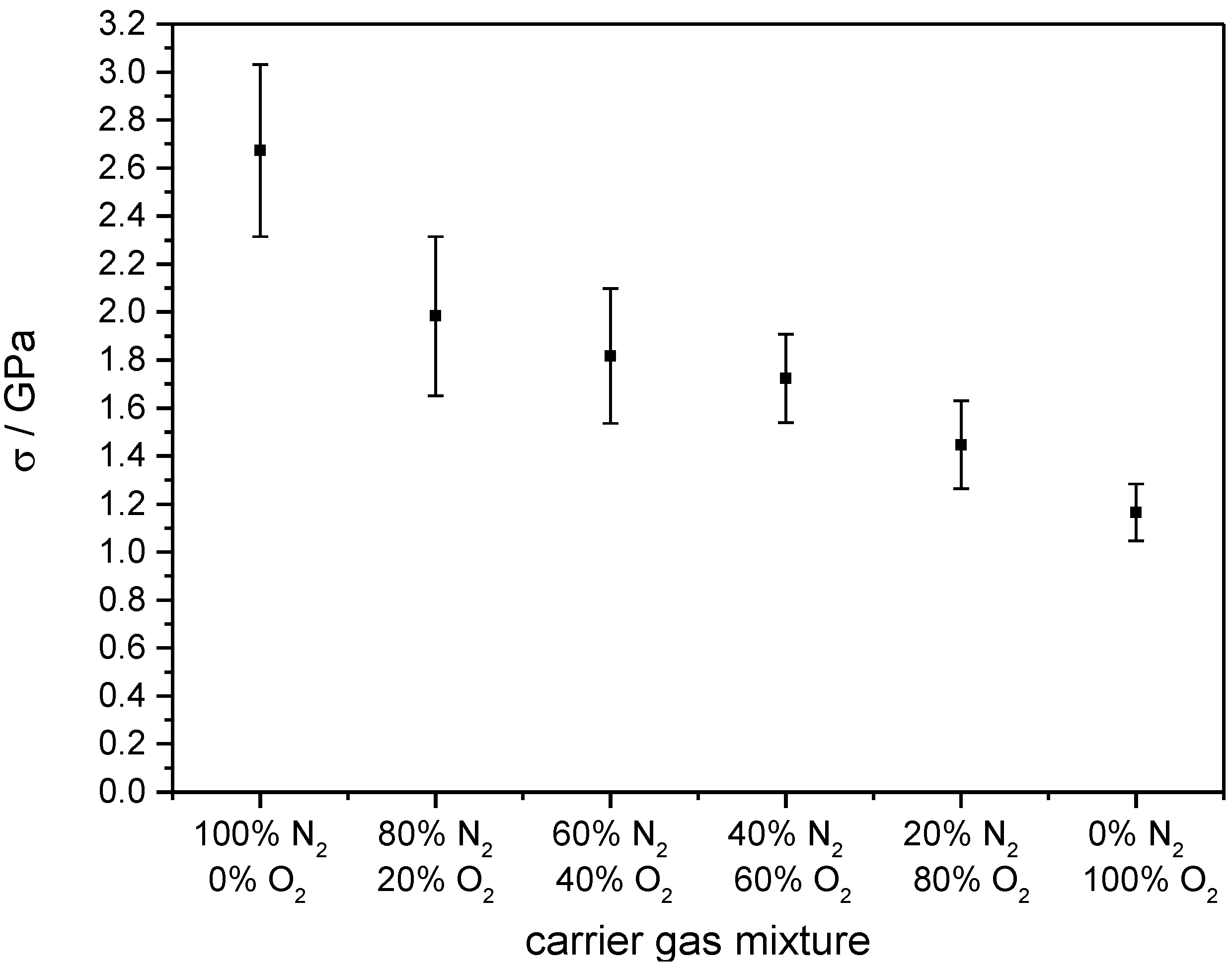
3.2. Carrier Gas Influence on Film Stress


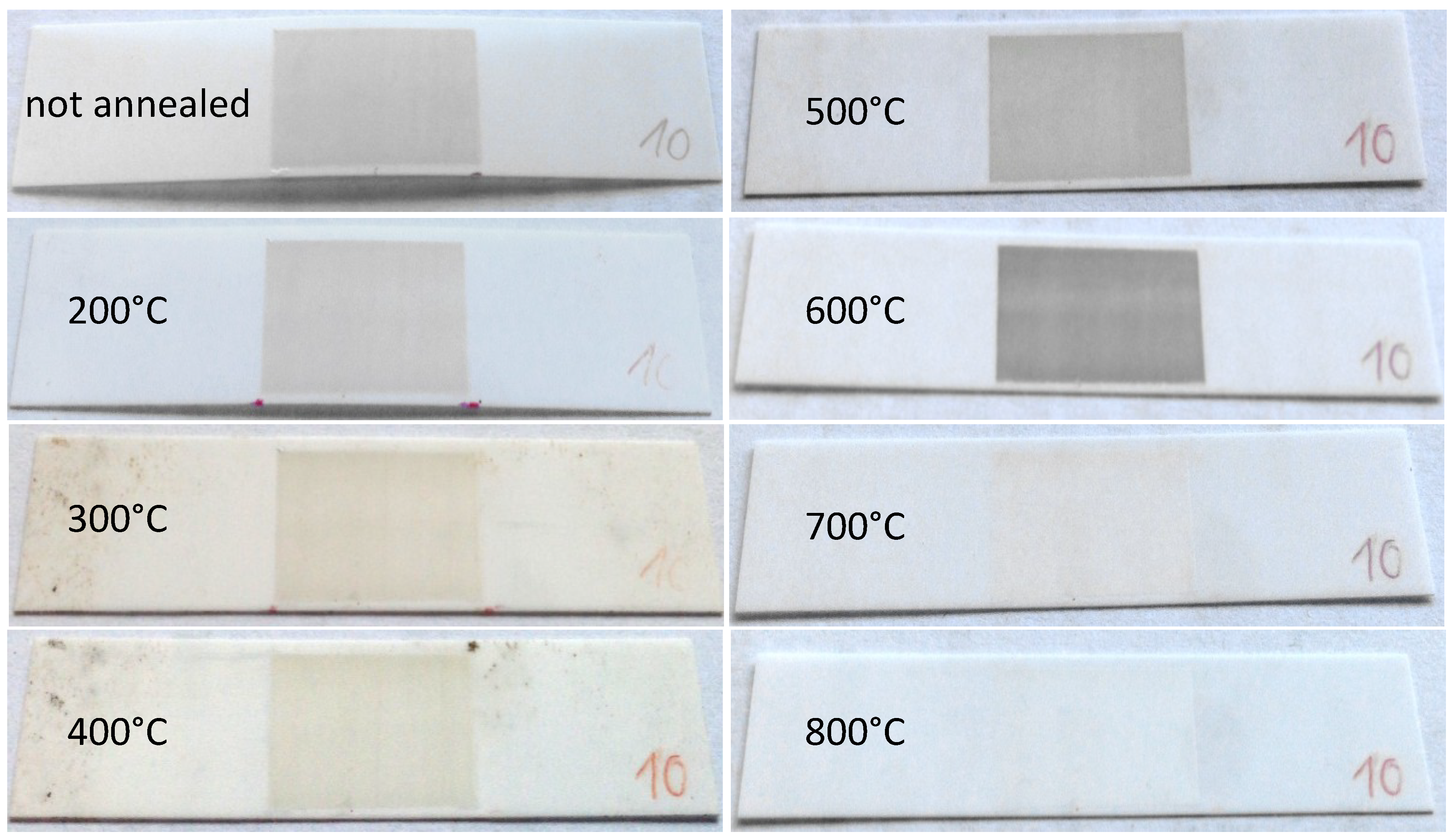
3.3. Annealing of Coated Al2O3 Substrates


4. Conclusions
Acknowledgments
Author Contributions
Conflicts of Interest
References
- Schatt, W.; Wieters, K.P.; Kieback, B. Pulvermetallurgie, Technologie und Werkstoffe; Springer: Berlin, Germany, 2007. (in German) [Google Scholar]
- Akedo, J. Room temperature impact consolidation (RTIC) of fine ceramic powder by aerosol deposition method and applications to microdevices. J. Therm. Spray Technol. 2008, 17, 181–196. [Google Scholar] [CrossRef]
- Akedo, J. Aerosol deposition method for fabrication of nano crystal ceramic layer. MSF 2004, 449–452, 43–48. [Google Scholar] [CrossRef]
- Akedo, J. Aerosol deposition of ceramic thick films at room temperature: Densification mechanism of ceramic layers. J. Am. Ceram. Soc. 2006, 89, 1834–1839. [Google Scholar] [CrossRef]
- Sahner, K.; Kaspar, M.; Moos, R. Assessment of the novel aerosol deposition method for room temperature preparation of metal oxide gas sensor films. Sens. Actuators B 2009, 139, 394–399. [Google Scholar] [CrossRef]
- Akedo, J. Ceramic coating at room temperature with aerosol deposition method. J. Vac. Soc. Jpn. 2011, 54, 118–127. [Google Scholar] [CrossRef]
- Lee, D.W.; Nam, S.M. Factors affecting surface roughness of Al2O3 films deposited on Cu substrates by an aerosol deposition method. J. Ceram. Process. Res. 2010, 11, 100–106. [Google Scholar]
- Johnson, S.D.; Kub, F.J.; Eddy, C.R., Jr. ZnS/Diamond composite coatings for infrared transmission applications formed by the aerosol deposition method. Proc. SPIE 2013, 8708. [Google Scholar] [CrossRef]
- Ryu, J.; Kim, K.J.; Choi, J.J.; Hahn, B.D.; Yoon, W.H.; Lee, B.K.; Park, D.S.; Jeong, D.Y.; Park, C. Flexible dielectric Bi1.5Zn1.0Nb1.5O7 thin films on a cu-polyimide foil. J. Am. Ceram. Soc. 2009, 92, 524–527. [Google Scholar] [CrossRef]
- Heo, Y.J.; Kim, H.T.; Kim, K.J.; Nahm, S.; Yoon, Y.J.; Kim, J. Enhanced heat transfer by room temperature deposition of AlN film on aluminum for a light emitting diode package. Appl. Therm. Eng. 2013, 50, 799–804. [Google Scholar] [CrossRef]
- Hirose, S.; Sakata, H.; Nakayama, C.; Koshizuka, N.; Murakami, M.; Akedo, J. Superconducting MgB2 thick films by AD process. In Proceedings of the 4th Tsukuba International Coatings Symposium, Tsukuba, Japan, 9–10 December 2010.
- Lee, D.W.; Kim, H.J.; Kim, Y.H.; Yun, Y.H.; Nam, S.M. Growth process of α-Al2O3 ceramic films on metal substrates fabricated at room temperature by aerosol deposition. J. Am. Ceram. Soc. 2011, 94, 3131–3138. [Google Scholar] [CrossRef]
- Cho, S.H.; Yoon, Y.J. Multi-layer TiO2 films prepared by aerosol deposition method for dye-sensitized solar cells. Thin Solid Films 2013, 547, 91–94. [Google Scholar] [CrossRef]
- Lee, B.K.; Jung, J.H.; Hahn, B.D.; Yoon, W.H.; Park, D.S.; Choi, J.J.; Ryu, J.; Kim, J.W.; Ahn, C.W.; Song, K.M. Dense yttria film deposited on a plasma-sprayed Al2O3 coating by aerosol deposition. J. Ceram. Sci. Technol. 2011, 2, 197–202. [Google Scholar]
- Akedo, J.; Lebedev, M. Piezoelectric properties and poling effect of Pb(Zr, Ti)O3 thick films prepared for microactuators by aerosol deposition. Appl. Phys. Lett. 2000, 77, 1710. [Google Scholar] [CrossRef]
- Kim, H.J.; Kim, Y.H.; Lee, J.W.; Nam, S.M.; Yoon, Y.J.; Kim, J.H. Residual stress relief in Al2O3-poly-tetra-fluoro-ethylene hybrid thick films for integrated substrates using aerosol deposition. J. Nanoelectron. Optoelectron. 2012, 7, 287–291. [Google Scholar] [CrossRef]
- Stoney, G. The tension of metallic films deposited by electrolysis. Proc. R. Soc. Lond. Ser. A Contain. Pap. Math. Phys. Character 1909, 82, 172–175. [Google Scholar]
- Gupta, T.K. Crack healing and strengthening of thermally shocked alumina. J. Am. Ceram. Soc. 1976, 59, 259–262. [Google Scholar] [CrossRef]
- Lange, F.F.; Gupta, T.K. Crack healing by heat treatment. J. Am. Ceram. Soc. 1970, 53, 54–55. [Google Scholar] [CrossRef]
- Case, E.D.; Smyth, J.R.; Hunter, O. Microcrack healing during the temperature cycling off single phase ceramics. In Fracture Mechanics of Ceramics; Bradt, R.C., Evans, A.G., Hasselmann, D.P.H., Lange, F.F., Eds.; Plenum Press: New York, NY, USA, 1983; Volume 5, pp. 507–530. [Google Scholar]
- Bandyopadhyay, G.; Kennedy, C.R. Isothermal crack healing and strength recovery in U2 subjected to varying degrees of thermal shock. J. Am. Ceram. Soc. 1977, 60, 48–50. [Google Scholar] [CrossRef]
- Wiederhorn, S.M.; Hockey, B.J.; Roberts, D.E. Effect of temperature on the fracture of sapphire. Philos. Mag. 1973, 28, 783–796. [Google Scholar] [CrossRef]
- Evans, A.G.; Charles, E.A. Strength recovery by diffusive crack healing. Acta Metall. 1977, 25, 919–927. [Google Scholar] [CrossRef]
- Apetz, R.; van Bruggen, M.P.B. Transparent alumina: A light-scattering model. J. Am. Ceram. Soc. 2003, 86, 480–486. [Google Scholar] [CrossRef]
© 2014 by the authors; licensee MDPI, Basel, Switzerland. This article is an open access article distributed under the terms and conditions of the Creative Commons Attribution license (http://creativecommons.org/licenses/by/3.0/).
Share and Cite
Schubert, M.; Exner, J.; Moos, R. Influence of Carrier Gas Composition on the Stress of Al2O3 Coatings Prepared by the Aerosol Deposition Method. Materials 2014, 7, 5633-5642. https://doi.org/10.3390/ma7085633
Schubert M, Exner J, Moos R. Influence of Carrier Gas Composition on the Stress of Al2O3 Coatings Prepared by the Aerosol Deposition Method. Materials. 2014; 7(8):5633-5642. https://doi.org/10.3390/ma7085633
Chicago/Turabian StyleSchubert, Michael, Jörg Exner, and Ralf Moos. 2014. "Influence of Carrier Gas Composition on the Stress of Al2O3 Coatings Prepared by the Aerosol Deposition Method" Materials 7, no. 8: 5633-5642. https://doi.org/10.3390/ma7085633