
Optical Properties and Plasmonic Performance of Titanium Nitride

Abstract
:1. Introduction
2. Results and Discussion
2.1. Fundamental Features and Methods of Growth
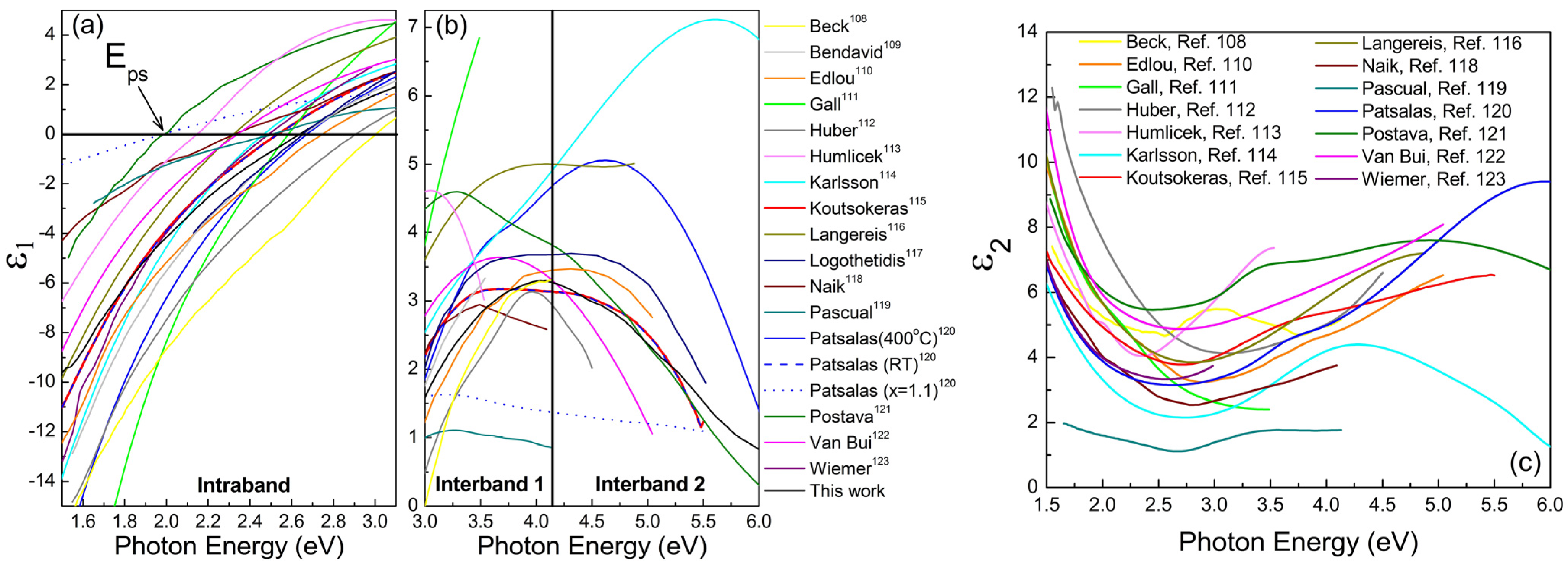
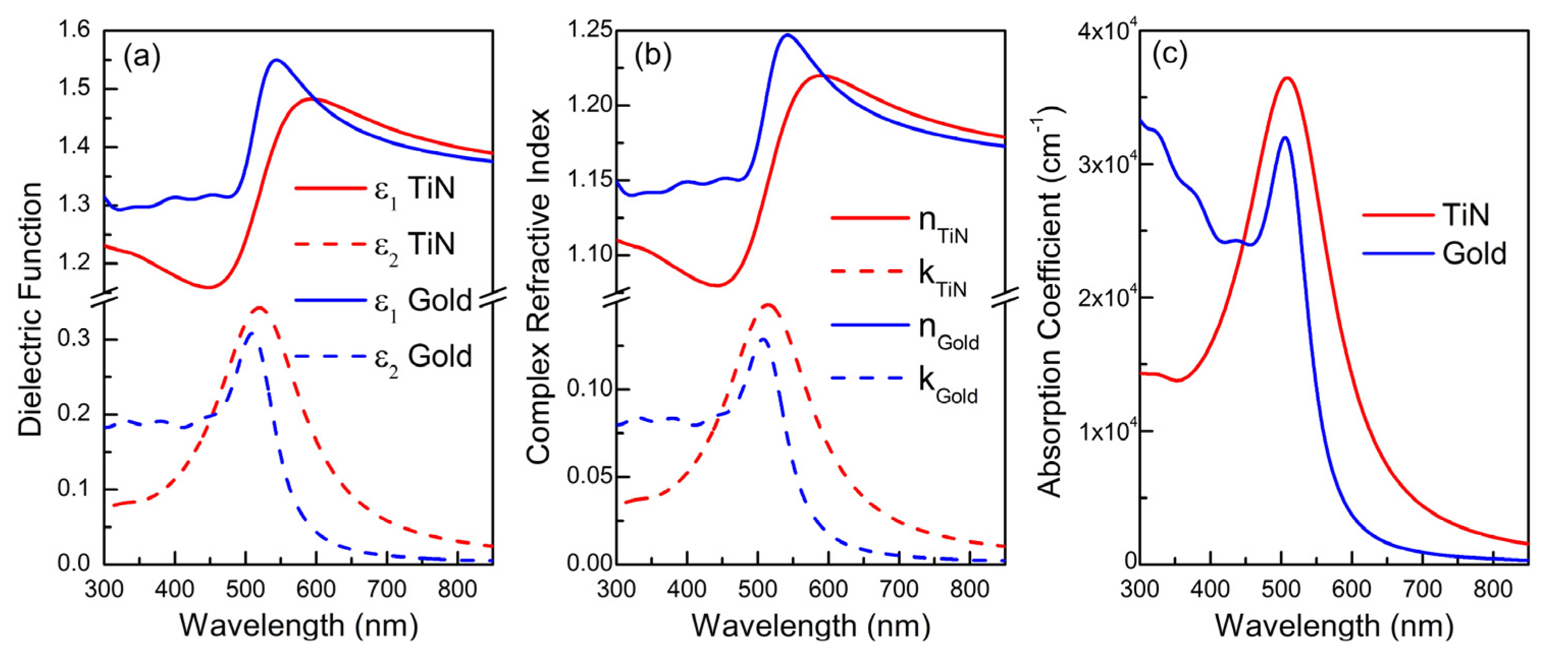
2.2. Optical Properties of TiN Films


| No | Growth Technique | Substrate | Thickness (nm) | Morphology | Measurement Technique # | Instrument * | Analysis Model | Reference | Comments |
|---|---|---|---|---|---|---|---|---|---|
| 1 | N/A | Stainless Steel | Opaque | N/A | SE | RPE by SOPRA | N/A | [108] | Stoichiometry determined by Auger Electron Spectroscopy (AES) |
| 2 | FCVA | Si(100) | 150 | N/A | SE | RAE | D | [109] | Stoichiometry x = 0.97 determined by Rutherford Backscattering (RBS) |
| 3 | Magnetron Sputtering | Fused Silica | Opaque | N/A | VASE | N/A | D+1L | [110] | Stoichiometry determined by RBS |
| 4 | UHV Sputtering | MgO(100) | 200 | Epitaxial | ORS | Perkin Elmer | D+2L | [111] | (100) Oriented identified by X-Ray Diffrcation (XRD); composition determined by RBS and X-Ray Photoelectron Spectroscopy (XPS); ORS measure-ments acquired using an integrating sphere; ORS normalization was performed via a Si(100) wafer |
| 5 | Me-PIII | Si(100) | 100–500 | Polycrystalline | SE | RAE | D+iL | [112] | Stoichiometry x = 0.95 determined by Elastic Recoil Detection Analysis (ERDA); crystal structure identified by XRD |
| 6 | IBAD | Si(100) | 50–100 | Polycrystalline | VASE | RAE | D+1L | [113] | Stoichiometry determined by XPS and RBS; crystal structure identified by XRD; existent O impurities |
| 7 | CVD | Polished Mo | ~1000 | Polycrystalline | ORS | Perkin Elmer | D+1L | [114] | Used TiCl4, H2, and N2 precursors; stoichiometry close to 1 determined by Electron Probe Microanalysis (EPMA) and by the cubic lattice size (0.424 nm) determined by XRD; no Cl impurities; C impurities <0.2% wt; Normalization of the spectra was performed via an evaporated Al mirror; Reflectivity spectra combined with Kramers-Kronig analysis to extract ε1, ε2 |
| 8 | DIBS | Si(100) | >300 | Globular polycrystalline | VASE | RPE by SOPRA | D+2L | [115] | Stoichiometry x = 1 determined by AES and XPS; crystal structure identified by XRD |
| 9 | ALD | H-terminated Si | >100 | Polycrystalline | in situ SE | RCE by J.A. Woolam | D+2L | [116] | Used TiCl4, H2, and N2 precursors; x < 1 |
| 10 | Magnetron Sputtering | Ti/Si(100) | 70 | Columnar Polycrystalline | in situ SE | PME by JY-Horiba | N/A | [117] | Microstructure identified by Transmission Electron Microscopy; no information on stoichiometry |
| 11 | Magnetron Sputtering | c-Sapphire | 30 | Epitaxial | VASE | RCE by J.A. Woolam | D+1L | [118] | The TiN[111]/Al2O3[0006] epitaxy was confirmed by XRD |
| 12 | PECVD | Glass | Opaque | N/A | SE | RAE | N/A | [119] | Used TiCl4, H2, and N2 precursors; no information on composition and structure |
| 13 | Magnetron Sputtering | Si(100) | >100 | Polycrystalline | in situ SE | PME by JY-Horiba | D+2L | [120] | Growth at 400 °C, Vb=-100 V; Stoichiometry close to 1 confirmed by XPS; crystal structure and (100) texture identified by XRD |
| 14 | Magnetron Sputtering | Si(100) | >100 | Polycrystalline | in situ SE | PME by JY-Horiba | D+2L | [120] | Growth at RT and Bias voltage of -120 V; Stoichiometry x = 1 determined by XPS; crystal structure and (100) texture identified by XRD |
| 15 | Magnetron Sputtering | Si(100) | >100 | Columnar Polycrystalline | in situ SE | PME by JY-Horiba | D+2L | [120] | Growth at RT and Vb = −20 V; Stoichiometry x = 1.12 determined by XPS; crystal structure and (111) texture identified by XRD |
| 16 | Sputtering | Thick thermal SiO2 | 107.1 | N/A | ORS | Shimadzu | D+2L | [121] | Spectral normalization was performed via a Si wafer |
| 17 | ALD | 100 nm thermal SiO2 | 10 | N/A | in situ SE | RCE by J.A. Woolam | D+2L | [122] | Used TiCl4 and NH3 precursors; Overstoichiometry determined by XPS; Existent Cl-impurities |
| 18 | Magnetron Sputtering | Si(100) | 400 | Polycrystalline | SE | PME by JY-Horiba | D | [123] | Stoichiometry 1.03 > x > 1 determined by ERDA; crystal structure identified by XRD |
| 19 | PLD | Si(100) | >100 | Polycrystalline | VASE | PME by JY-Horiba | D+2L | This work | Growth at Room Temperature; Stoichiometry x = 1 determined by in situ XPS; crystal structure and (111) texture identified by XRD |
| 20 | Magnetron Sputtering | Glass | N/A | N/A | SE | Null Ellips. | N/A | [124] | Measurement acquired at 70° angle of incidence and in p-polarization |
| 21 | N/A | N/A | N/A | N/A | ORS | N/A | N/A | [125] | Reflectivity confirmed by ab initio calculations for stoichiometric TiN |
| 22 | Plasma-assisted Evaporation | Si or Glass | 85 | Polycrystalline | in situ SE | N/A | N/A | [126] | Reduced reflectivity values due to short thickness (films not completely opaque) |
| 23 | Magnetron Sputtering | Ck35 Carbon steel | N/A | Columnar Polycrystalline | SE | RAE | N/A | [127] | Stoichiometry determined by EPMA; crystal structure identified by XRD |
| 24 | Magnetron Sputtering | Stainless steel | >2000 | Polycrystalline | ORS | Beckman | D | [128] | Stoichiometry determined by EPMA; crystal structure identified by XRD |


| Reference | Intraband | Interband 1 | Interband 2 | Composite | Properties | |||||||
|---|---|---|---|---|---|---|---|---|---|---|---|---|
| Epu (eV) | Γd (eV) | f1 | E01 (eV) | γ1 (eV) | f2 | E02 (eV) | γ2 (eV) | Eps (eV) | ε∞ | MFP (nm) | ρ(μΩ cm) | |
| Edlou et al. [110] | 7.248 | 0.639 | 0.232 | 2.066 | 0.544 | 4.039 | 5.645 | 3.621 | 2.75 | 2.352 | 19.9 | 94 |
| Gall et al. [111] | 9.766 | 0.349 | 0.395 | 2.195 | 0.816 | 5.278 | 8.228 | 4.041 | 2.59 | 8.784 | 56.5 | 28 |
| Huber et al. [112] | 8.080 | 0.860 | 3.536 | 5.139 | 3.043 | N/A | N/A | N/A | 2.90 | 2.998 | 14.9 | 102 |
| Humlicek et al. [113] | 6.421 | 0.859 | 3.118 | 3.765 | 1.547 | N/A | N/A | N/A | 2.15 | 3.839 | 12.8 | 161 |
| Koutsokeras et al. [115] | 7.051 | 0.629 | 0.383 | 3.713 | 1.333 | 4.349 | 5.878 | 4.282 | 2.55 | 2.129 | 20.0 | 98 |
| Langereis et al. [116] | 7.210 | 0.806 | 2.685 | 4.480 | 2.644 | 1.274 | 5.355 | 0.879 | 2.32 | 3.871 | 15.0 | 120 |
| Naik et al. [118] | 5.707 | 0.165 | 0.195 | 2.264 | 0.722 | 2.312 | 4.894 | 3.875 | 1.99 | 2.667 | 247.3 | 39 |
| Patsalas et al. [12] 400 °C, Vb = −100 V | 7.750 | 0.350 | 0.100 | 3.682 | 0.712 | 5.620 | 6.260 | 3.875 | 2.67 | 1.850 | 48.2 | 45 |
| Patsalas et al. [120] RT, Vb = −120 V | 6.926 | 0.589 | 0.183 | 3.690 | 0.943 | 4.877 | 5.967 | 4.882 | 2.65 | 1.872 | 21.5 | 95 |
| Patsalas et al. [120] RT, Vb = −40 V, x = 1.1 | 4.493 | 1.379 | 0.550 | 3.761 | 2.075 | 1.639 | 6.674 | 5.553 | 1.98 | 1.198 | 5.9 | 527 |
| Postava et al. [121] | 6.357 | 0.738 | 0.146 | 3.478 | 0.760 | 7.008 | 5.789 | 5.933 | 1.99 | 1.957 | 15.3 | 141 |
| Wiemer et al. [123] | 7.067 | 0.438 | 4.218 | 5.084 | 3.349 | N/A | N/A | N/A | 2.48 | 3.236 | 32.4 | 68 |
| TiN by PLD, this work | 6.944 | 0.726 | 3.962 | 5.521 | 4.117 | 1.041 | 7.823 | 2.199 | 2.64 | 1.198 | 16.5 | 116 |
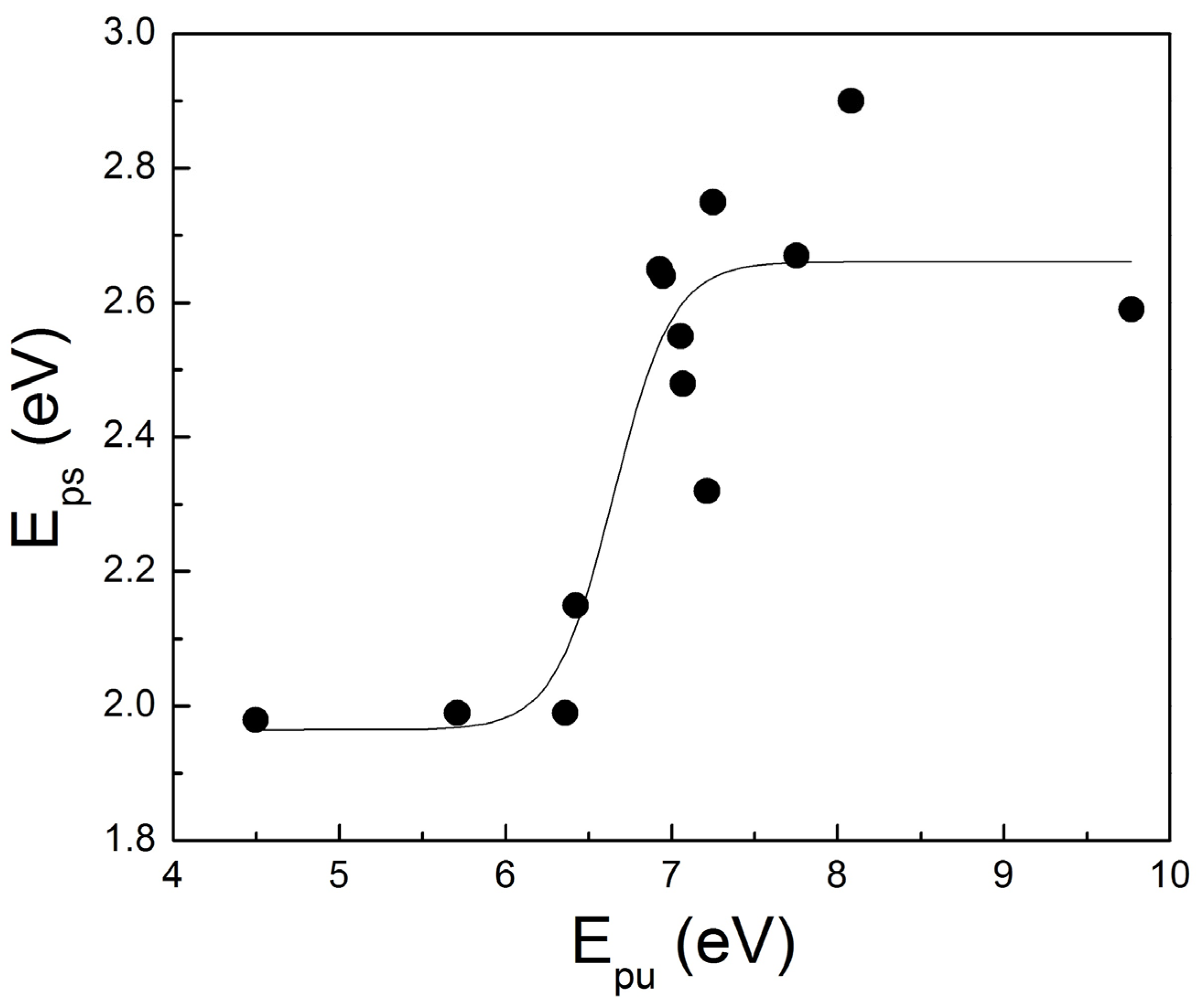
- (1)
- The maximum MFP acquired for the reported TiN films is less than 50 nm; this value, compared with equivalent values for noble metals, can provide a measure of the size limitations for single-crystalline TiN nanoparticles, which might exhibit LSPR,
- (2)
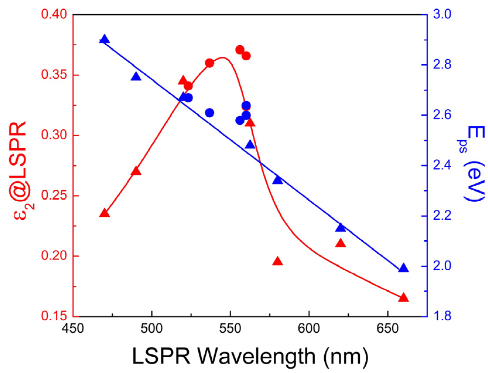
- Eps, which is associated with the SPP performance of TiN as we will show below, is associated only with Epu (see also Figure 5) and there is no explicit relation of Eps with any other D2L parameter. The meaning of this observation is that, despite that the screening of the plasma energy in TiN is due to the existence of the interband transitions, similar to Au, the numerical variations of these interband transitions are not strong enough to affect Eps.
- (3)
- Epu, which is associated with the conduction electron density, is above 6.9 eV for stoichiometric and highly conductive TiN; the same films exhibit Eps close to 2.65 eV as observed by Logothetidis et al. [117].

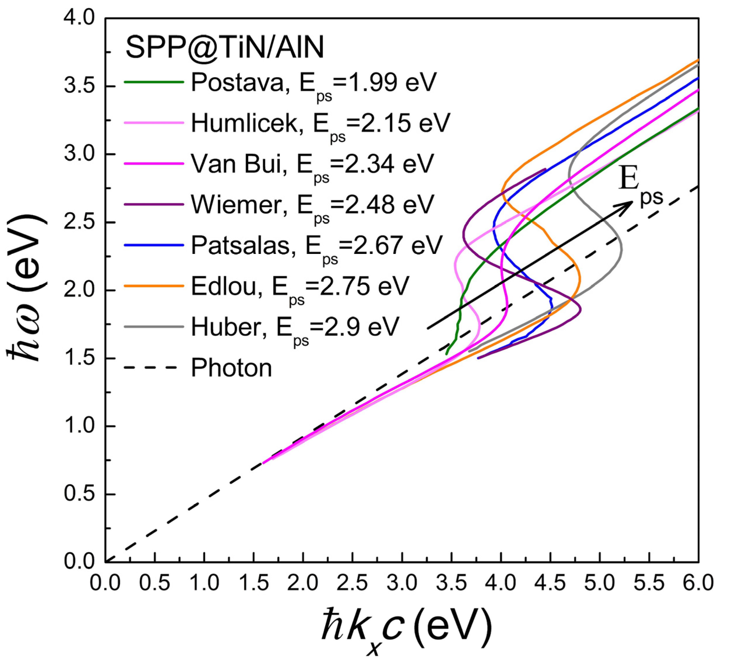
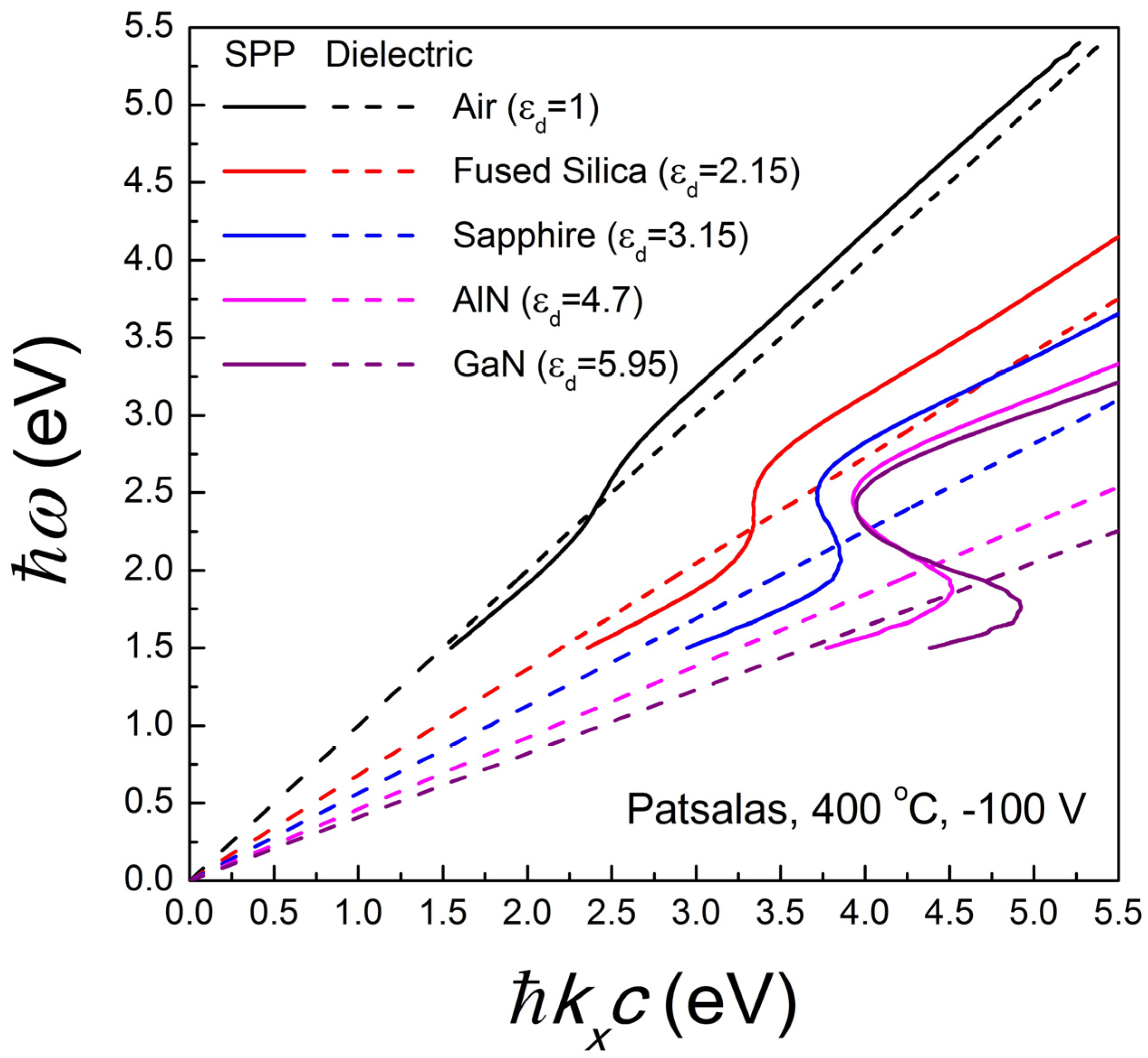
2.3. Potential of TiN for SPP Applications


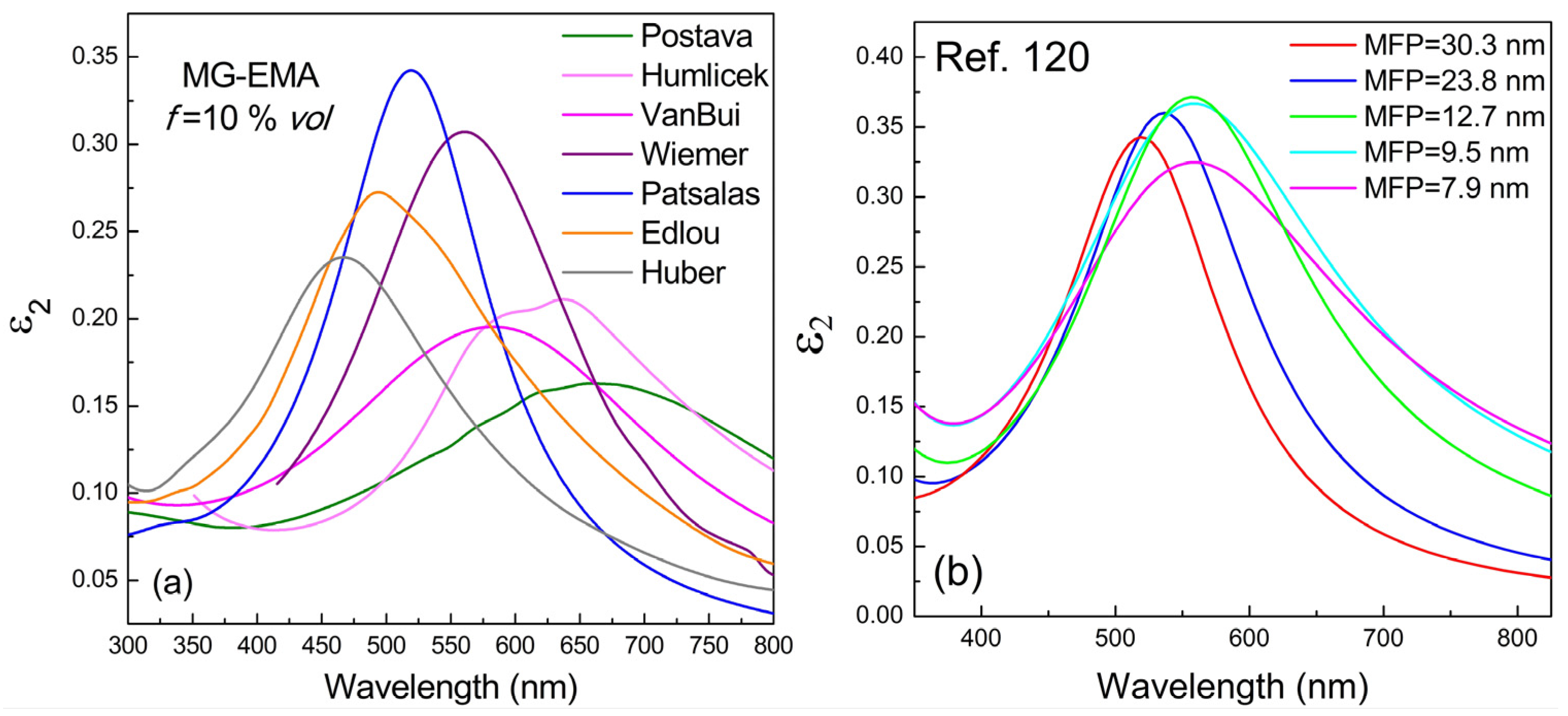
2.3. Potential of TiN for LSPR Applications


3. Conclusions
Author Contributions
Conflicts of Interest
References
- Perry, A.J. A contribution to the study of Poisson’s ratios and elastic constants of TiN, ZrN and HfN. Thin Solid Films 1990, 193–194, 463–471. [Google Scholar] [CrossRef]
- Kuzel, R., Jr.; Cerny, R.; Valvoda, V.; Blomberg, M.; Merisalo, M. Complex XRD microstructural studies of hard coatings applied to PVD-deposited TiN films. Thin Solid Films 1994, 247, 64–78. [Google Scholar] [CrossRef]
- Sproul, W.D.; Rudnik, P.J.; Gogol, C.A. The effect of target power on the nitrogen partial pressure level and hardness of reactively sputtered titanium nitride coatings. Thin Solid Films 1989, 171, 171–181. [Google Scholar] [CrossRef]
- Gammer, K.; Stoiber, M.; Wagner, J.; Hutter, H.; Kullmer, R.; Mitterer, C. Investigations on the effects of plasma-assisted pre-treatment for plasma-assisted chemical vapour deposition TiN coatings on tool steel. Thin Solid Films 2004, 461, 277–281. [Google Scholar] [CrossRef]
- Östling, M.; Nygren, S.; Petersson, C.S.; Norström, H.; Buchta, R.; Blom, H.-O.; Berg, S. A comparative study of the diffusion barrier properties of TiN and ZrN. Thin Solid Films 1986, 145, 81–88. [Google Scholar] [CrossRef]
- Kaloyeros, A.E.; Eisenbraun, E. Ultrathin diffusion barriers/liners for gigascale copper metallization. Annu. Rev. Mater. Sci. 2000, 30, 363–385. [Google Scholar] [CrossRef]
- Chen, G.S.; Huang, S.C.; Chen, S.T.; Yang, T.J.; Lee, P.Y.; Jou, J.H.; Lin, T.C. An optimal quasisuperlattice design to further improve thermal stability of tantalum nitride diffusion barriers. Appl. Phys. Lett. 2000, 76, 2895–2897. [Google Scholar] [CrossRef]
- Zeng, Y.; Russell, S.W.; McKerrow, A.J.; Chen, L.; Alford, T.L. Effectiveness of Ti, TiN, Ta, TaN, and W2N as barriers for the integration of low-k dielectric hydrogen silsesquioxane. J. Vac. Sci. Technol. B 2000, 18, 221–230. [Google Scholar] [CrossRef]
- Aouadi, S.M.; Shreeman, P.K.; Williams, M. Real-time spectroscopic ellipsometry study of ultrathin diffusion barriers for integrated circuits. J. Appl. Phys. 2004, 96, 3949–3955. [Google Scholar] [CrossRef]
- Randhawa, H. Hard coatings for decorative applications. Surf. Coat. Technol. 1988, 36, 829–836. [Google Scholar] [CrossRef]
- Budke, E.; Krempel-Hesse, J.; Maidhof, H.; Schüssler, H. Decorative hard coatings with improved corrosion resistance. Surf. Coat. Technol. 1999, 112, 108–113. [Google Scholar] [CrossRef]
- Niyomsoan, S.; Grant, W.; Olson, D.L.; Mishra, B. Variation of color in titanium and zirconium nitride decorative thin films. Thin Solid Films 2002, 415, 187–194. [Google Scholar] [CrossRef]
- Petrov, I.; Barna, P.B.; Hultman, L.; Greene, J.E. Microstructural evolution during film growth. J. Vac. Sci. Technol. A 2003, 21, S117–S128. [Google Scholar] [CrossRef]
- Patsalas, P.; Logothetidis, S. Interface properties and structural evolution of TiN/Si and TiN/GaN heterostructures. J. Appl. Phys. 2003, 93, 989–998. [Google Scholar] [CrossRef]
- Matenoglou, G.M.; Koutsokeras, L.E.; Patsalas, P. Plasma energy and work function of conducting transition metal nitrides for electronic applications. Appl. Phys. Lett. 2009, 94, 152108. [Google Scholar] [CrossRef]
- Koutsokeras, L.E.; Matenoglou, G.M.; Patsalas, P. Structure, electronic properties and electron energy loss spectra of transition metal nitride films. Thin Solid Films 2013, 528, 49–52. [Google Scholar] [CrossRef]
- Ruterana, P.; Nouet, G.; Kehagias, Th.; Komninou, Ph.; Karakostas, Th.; di Fort-Poisson, M.A.; Huet, F.; Morkoc, H. Microstructure of Ti/Al and TiN Ohmic contacts to gallium nitride. Phys. Stat. Sol. A 1999, 176, 767–771. [Google Scholar] [CrossRef]
- Gautier, S.; Komninou, Ph.; Patsalas, P.; Kehagias, Th.; Logothetidis, S.; Dimitriadis, C.A.; Nouet, G. Optical and electrical properties of TiN/n-GaN contacts in correlation with their structural properties. Semiconduct. Sci. Technol. 2003, 18, 594–601. [Google Scholar] [CrossRef]
- Patsalas, P.; Charitidis, C.; Logothetidis, S.; Dimitriadis, C.A.; Valassiades, O. Combined electrical and mechanical properties of titanium nitride thin films as metallization materials. J. Appl. Phys. 1999, 86, 5296–5298. [Google Scholar] [CrossRef]
- Malmros, A.; Andersson, K.; Rorsman, N. Combined TiN- and TaN temperature compensated thin film resistors. Thin Solid Films 2012, 520, 2162–2165. [Google Scholar] [CrossRef]
- Ernsberger, C.; Perry, A.J.; Lehman, L.P.; Miller, A.E.; Pelton, A.R.; Dabrowski, B.W. Low temperature tempering-induced changes in bulk resistivity, temperature coefficient of resistivity and stress in physically vapor-deposited TiN. Surf. Coat. Technol. 1988, 36, 605–616. [Google Scholar] [CrossRef]
- Hultman, L.; Ljungcrantz, H.; Hallin, C.; Janzén, E.; Sundgren, J.-E.; Pécz, B.; Wallenberg, L.R. Growth and electronic properties of epitaxial TiN thin films on 3C-SiC(001) and 6H-SiC(0001) substrates by reactive magnetron sputtering. J. Mater. Res. 1996, 11, 2458–2462. [Google Scholar] [CrossRef]
- Dimitriadis, C.A.; Lee, J.I.; Patsalas, P.; Logothetidis, S.; Tassis, D.H.; Brini, J.; Kamarinos, G. Characteristics of TiNx/n-Si Schottky diodes deposited by reactive magnetron sputtering. J. Appl. Phys. 1999, 85, 4238–4242. [Google Scholar]
- Petrov, I.; Hultman, L.; Helmersson, U.; Sundgren, J.-E.; Greene, J.E. Microstructure modification of TiN by ion bombardment during reactive sputter deposition. Thin Solid Films 1989, 169, 299–314. [Google Scholar] [CrossRef]
- Wagner, J.; Mitterer, C.; Penoy, M.; Michotte, C.; Wallgram, W.; Kathrein, M. The effect of deposition temperature on microstructure and properties of thermal CVD TiN coatings. Int. J. Refract. Met. Hard Mater. 2008, 26, 120–126. [Google Scholar] [CrossRef]
- Perry, A.J.; Strandberg, C.; Sproul, W.D.; Hofmann, S.; Ernsberger, C.; Nickerson, J.; Chollet, L. The chemical analysis of TiN films: A round robin experiment. Thin Solid Films 1987, 153, 169–183. [Google Scholar] [CrossRef]
- Musil, J.; Poulek, V.; Valvoda, V.; Kužel, R., Jr.; Jehn, H.A.; Baumgärtner, M.E. Relation of deposition conditions of Ti-N films prepared by d.c. magnetron sputtering to their microstructure and macrostress. Surf. Coat. Technol. 1993, 60, 484–488. [Google Scholar] [CrossRef]
- Abadias, G.; Tse, Y.Y. Diffraction stress analysis in fiber-textured TiN thin films grown by ion-beam sputtering: Application to (001) and mixed (001)+(111) texture. J. Appl. Phys. 2004, 95, 2414–2428. [Google Scholar] [CrossRef]
- Gbordzoe, S.; Kotoka, R.; Craven, E.; Kumar, D.; Wu, F.; Narayan, J. Effect of substrate temperature on the microstructural properties of titanium nitride nanowires grown by pulsed laser deposition. J. Appl. Phys. 2014, 116, 064310. [Google Scholar] [CrossRef]
- Evangelou, E.K.; Konofaos, N.; Aslanoglou, X.A.; Dimitriadis, C.A.; Patsalas, P.; Logothetidis, S.; Kokkoris, M.; Kossionides, E.; Vlastou, R.; Groetschel, R. Characterization of magnetron sputtering deposited thin films of TiN for use as a metal electrode on TiN/SiO2/Si metal-oxide-semiconductor device. J. Appl. Phys. 2000, 88, 7192–7196. [Google Scholar] [CrossRef]
- Majhi, P.; Wen, H.-C.; Choi, K.; Alshareef, H.; Huffman, C.; Lee, B.H. A Systematic Study of the Influence of Nitrogen in Tuning the Effective Work Function of Nitrided Metal Gates. In In Proceeding of the IEEE VLSI-TSA Int. Symp. on VLSI Technology, Hsinchu, Taiwan, 25–27 April 2005; pp. 105–106.
- Maier, S.A. Plasmonics: Fundamentals and Applications; Springer Science and Business Media LLC: New York, NY, USA, 2007; pp. 65–87. [Google Scholar]
- Enoch, S.; Bonod, N. Plasmonics: From Basics to Advanced Topics; Springer Science and Business Media LLC: New York, NY, USA, 2007; pp. 105–148, 151–176. [Google Scholar]
- Berini, P.; de Leon, I. Surface plasmon-polariton amplifiers and lasers. Nat. Phot. 2012, 6, 16–24. [Google Scholar] [CrossRef]
- Lal, S.; Link, S.; Halas, N.J. Nano-optics from sensing to waveguiding. Nat. Phot. 2007, 1, 641–648. [Google Scholar] [CrossRef]
- Barnes, W.L.; Dereux, A.; Ebbesen, T.W. Surface plasmon subwavelength optics. Nature 2003, 424, 824–830. [Google Scholar] [CrossRef] [PubMed]
- Polman, A. Applied physics: Plasmonics applied. Science 2008, 322, 868–869. [Google Scholar] [CrossRef] [PubMed]
- Ozbay, E. Plasmonics: Merging photonics and electronics at nanoscale dimensions. Science 2006, 311, 189–193. [Google Scholar] [CrossRef] [PubMed]
- Brongersma, M.L.; Shalaev, V.M. The Case for Plasmonics. Science 2010, 328, 440–441. [Google Scholar] [CrossRef] [PubMed]
- Van Duyne, R.P. Molecular Plasmonics. Science 2004, 306, 985–986. [Google Scholar] [CrossRef] [PubMed]
- Dionne, J.A.; Diest, K.; Sweatlock, L.A.; Atwater, H.A. PlasMOStor: A Metal−Oxide−Si Field Effect Plasmonic Modulator. Nano Lett. 2009, 9, 897–902. [Google Scholar] [CrossRef] [PubMed]
- Lin, J.; Li, H.; Zhang, H.; Chen, W. Plasmonic enhancement of photocurrent in MoS2 field-effect-transistor. Appl. Phys. Lett. 2013, 102, 203109. [Google Scholar] [CrossRef]
- Wang, L.; Hu, W.; Wang, J.; Wang, X.; Wang, S.; Chen, X.; Lu, W. Plasmon resonant excitation in grating-gated AlN barrier transistors at terahertz frequency. Appl. Phys. Lett. 2012, 100, 123501. [Google Scholar] [CrossRef]
- Sheldon, M.T.; De Groep, J.V.; Brown, A.M.; Polman, A.; Atwater, H.A. Plasmoelectric potentials in metal nanostructures. Science 2014, 346, 828–831. [Google Scholar] [CrossRef] [PubMed]
- Anker, J.N.; Hall, W.P.; Lyandres, O.; Shah, N.C.; Zhao, J.; Van Duyne, R.P. Biosensing with plasmonic Nanosensors. Nat. Mater. 2008, 7, 442–453. [Google Scholar] [CrossRef] [PubMed]
- Zhang, B.; Kumar, R.B.; Dai, H.; Feldman, B.J. A plasmonic chip for biomarker discovery and diagnosis of type 1 diabetes. Nat. Med. 2014, 20, 948–953. [Google Scholar] [CrossRef] [PubMed]
- Zhang, R.; Zhang, Y.; Dong, Z.C.; Jiang, S.; Zhang, C.; Chen, L.G.; Zhang, L.; Liao, Y.; Aizpurua, J.; Luo, Y.; et al. Chemical mapping of a single molecule by plasmon-enhanced Raman scattering. Nature 2013, 498, 82–86. [Google Scholar] [CrossRef] [PubMed]
- Kravets, V.G.; Schedin, F.; Jalil, R.; Britnell, L.; Gorbachev, R.V.; Ansell, D.; Thackray, B.; Novoselov, K.S.; Geim, A.K.; Kabashin, A.V.; et al. Singular phase nano-optics in plasmonic metamaterials for label-free single-molecule detection. Nat. Mater. 2013, 12, 304–309. [Google Scholar] [CrossRef] [PubMed]
- De Angelis, F.; Das, G.; Candeloro, P.; Patrini, M.; Galli, M.; Bek, A. Nanoscale chemical mapping using three-dimensional adiabatic compression of surface plasmon polaritons. Nat. Nanotech. 2010, 5, 67–72. [Google Scholar] [CrossRef] [PubMed]
- Mubeen, S.; Lee, J.; Singh, N.; Krämer, S.; Stucky, G.D.; Moskovits, M. An autonomous photosynthetic device in which all charge carriers derive from surface plasmons. Nat. Nanotech. 2013, 8, 247–251. [Google Scholar] [CrossRef] [PubMed]
- Qian, K.; Sweeny, B.C.; Johnston-Peck, A.C.; Niu, W.; Graham, J.O.; Duchene, J.S.; Qiu, J.; Wang, Y.-C.; Engelhard, M.H.; Su, D.; et al. Surface plasmon-driven water reduction: Gold nanoparticle size matters. J. Am. Chem. Soc. 2014, 136, 9842–9845. [Google Scholar] [CrossRef] [PubMed]
- Wang, Z.; Yang, C.; Lin, T.; Yin, H.; Chen, P.; Wan, D.; Xu, F.; Huang, F.; Lin, J.; Xie, X.; Jiang, M. H-doped black titania with very high solar absorption and excellent photocatalysis enhanced by localized surface plasmon resonance. Adv. Funct. Mater. 2013, 23, 5444–5450. [Google Scholar] [CrossRef]
- Larsson, E.M.; Langhammer, C.; Zoric, I.; Kasemo, B. Nanoplasmonic Probes of Catalytic Reactions. Science 2009, 326, 1091–1094. [Google Scholar] [CrossRef] [PubMed]
- Atwater, H.A.; Polman, A. Plasmonics for Improved Photovoltaic Devices. Nat. Mater. 2010, 9, 205–213. [Google Scholar] [CrossRef] [PubMed]
- Aubry, A.; Lei, D.Y.; Fernandez-Dominguez, A.I.; Sonnefraud, Y.; Maier, S.A.; Pendry, J.B. Plasmonic Light-Harvesting Devices over the Whole Visible Spectrum. Nano Lett. 2010, 10, 2574–2579. [Google Scholar] [CrossRef] [PubMed]
- Pelayo García De Arquer, F.; Mihi, A.; Konstantatos, G. Molecular interfaces for plasmonic hot electron photovoltaics. Nanoscale 2015, 7, 2281–2288. [Google Scholar] [CrossRef] [PubMed]
- Gan, Q.; Bartoli, F.J.; Kafafi, Z.H. Plasmonic-enhanced organic photovoltaics: Breaking the 10% efficiency barrier. Adv. Mater. 2013, 25, 2385–2396. [Google Scholar] [CrossRef] [PubMed]
- Stratakis, E.; Kymakis, E. Nanoparticle-based plasmonic organic photovoltaic devices. Mater. Today 2013, 16, 133–146. [Google Scholar] [CrossRef]
- Kalfagiannis, N.; Karagiannidis, P.G.; Pitsalidis, C.; Panagiotopoulos, N.T.; Gravalidis, C.; Kassavetis, S.; Patsalas, P.; Logothetidis, S. Plasmonic silver nanoparticles for improved organic solar cells. Sol. Energy Mater. Sol. Cells 2012, 104, 165–174. [Google Scholar] [CrossRef]
- Deceglie, M.G.; Ferry, V.E.; Alivisatos, A.P.; Atwater, H.A. Design of nanostructured solar cells using coupled optical and electrical modeling. Nano Lett. 2012, 12, 2894–2900. [Google Scholar] [CrossRef] [PubMed]
- Pala, R.A.; Liu, J.S.Q.; Barnard, E.S.; Askarov, D.; Garnett, E.C.; Fan, S.; Brongersma, M.L. Optimization of non-periodic plasmonic light-trapping layers for thin-film solar cells. Nat. Commun. 2013, 4, 2095. [Google Scholar] [CrossRef] [PubMed]
- Sobhani, A.; Knight, M.W.; Wang, Y.; Zheng, B.; King, N.S.; Brown, L.V.; Fang, Z.; Nordlander, P.; Halas, N.J. Narrowband photodetection in the near-infrared with a plasmon-induced hot electron device. Nat. Commun. 2013, 4, 1643. [Google Scholar] [CrossRef] [PubMed]
- Konstantatos, G.; Sargent, E.H. Nanostructured materials for photon detection. Nat. Nanotech. 2010, 5, 391–400. [Google Scholar] [CrossRef] [PubMed]
- Chalabi, H.; Schoen, D.; Brongersma, M.L. Hot-electron photodetection with a plasmonic nanostripe antenna. Nano Lett. 2014, 14, 1374–1380. [Google Scholar] [CrossRef] [PubMed]
- Montelongo, Y.; Tenorio-Pearl, J.O.; Williams, C.; Zhang, S.; Milne, W.I.; Wilkinson, T.D. Plasmonic nanoparticle scattering for color holograms. Proc. Natl. Acad. Sci. USA 2014, 111, 12679–12683. [Google Scholar] [CrossRef] [PubMed]
- Olson, J.; Manjavacas, A.; Liu, L.; Chang, W.-S.; Foerster, B.; King, N.S.; Knight, M.W.; Nordlander, P.; Halas, N.J.; Link, S. Vivid, full-color aluminum plasmonic pixels. Proc. Natl. Acad. Sci. USA 2014, 111, 14348–14353. [Google Scholar] [CrossRef] [PubMed]
- Siozios, A.; Koutsogeorgis, D.C.; Lidorikis, E.; Dimitrakopoulos, G.P.; Kehagias, T.; Zoubos, H.; Komninou, P.; Cranton, W.M.; Kosmidis, C.; Patsalas, P. Optical Encoding by Plasmon-Based Patterning: Hard and Inorganic Materials Become Photosensitive. Nano Lett. 2012, 12, 259–263. [Google Scholar] [CrossRef] [PubMed]
- Zijlstra, P.; Chon, J.W.M.; Gu, M. Five-Dimensional Optical Recording Mediated by Surface Plasmons in Gold Nanorods. Nature 2009, 459, 410–413. [Google Scholar] [CrossRef] [PubMed]
- Wan, D.; Chen, H.-L.; Tseng, S.-C.; Wang, L.A.; Chen, Y.-P. One-Shot Deep-UV–Pulsed laser-induced photomodification of hollow metal nanoparticles for high density data storage on flexible substrates. ACS Nano 2010, 4, 165–173. [Google Scholar] [CrossRef] [PubMed]
- Sanchez-Valencia, J.R.; Toudert, J.; Borras, A.; Barranco, A.; Lahoz, R.; de la Fuente, G.F.; Frutos, F.; Gonzalez-Elipe, A.R. Selective Dichroic Patterning by Nanosecond Laser Treatment of Ag Nanostripes. Adv. Mater. 2011, 23, 848–853. [Google Scholar] [CrossRef] [PubMed]
- Asoro, M.A.; Damiano, J.; Ferreira, P.J. Size Effects on the Melting Temperature of Silver Nanoparticles: In-situ TEM Observations. Microsc. Microanal. 2009, 15, 706–707. [Google Scholar] [CrossRef]
- Chernyshev, A.P. Effect of Nanoparticle Size on the Onset Temperature of Surface Melting. Mater. Lett. 2009, 63, 1525–1527. [Google Scholar] [CrossRef]
- Alarifi, H.A.; Atiş, M.; Özdoğan, C.; Hu, A.; Yavuz, M.; Zhou, Y. Determination of Complete Melting and Surface Premelting Points of Silver Nanoparticles by Molecular Dynamics Simulation. J. Phys. Chem. C 2013, 117, 12289–12298. [Google Scholar] [CrossRef]
- Matula, R.A. Electrical resistivity of copper, gold palladium and silver. J. Phys. Chem. Ref. Data 1979, 8, 1147–1298. [Google Scholar] [CrossRef]
- Boltasseva, A.; Atwater, H.A. Low-Loss Plasmonic Metamaterials. Science 2011, 331, 290–291. [Google Scholar] [CrossRef] [PubMed]
- Poulek, V.; Musil, J.; Valvoda, V.; Cerny, R. Microhardness of Ti-N films containing the ε-Ti2N phase. J. Phys. D 1988, 21, 1657–1658. [Google Scholar] [CrossRef]
- Rauschenbach, B. Formation of compounds by high-flux nitrogen ion implantation in titanium. J. Mater. Sci. 1986, 21, 395–404. [Google Scholar] [CrossRef]
- Xu, M.; Wang, S.; Yin, G.; Li, J.; Zheng, Y.; Chen, L.; Jia, Y. Optical properties of cubic Ti3N4, Zr3N4, and Hf3N4. Appl. Phys. Lett. 2006, 89, 151908. [Google Scholar] [CrossRef]
- Kroll, P. Hafnium nitride with thorium phosphide structure: Physical properties and an assessment of the Hf-N, Zr-N, and Ti-N phase diagrams at high pressures and temperatures. Phys. Rev. Lett. 2003, 90, 12550. [Google Scholar] [CrossRef]
- Stampfl, C.; Mannstadt, W.; Asahi, R.; Freeman, A.J. Electronic structure and physical properties of early transition metal mononitrides: Density-functional theory LDA, GGA, and screened-exchange LDA FLAPW calculations. Phys. Rev. B 2001, 63, 155106. [Google Scholar] [CrossRef]
- Brik, M.G.; Ma, C.-G. First-principles studies of the electronic and elastic properties of metal nitrides XN (X = Sc, Ti, V, Cr, Zr, Nb). Comp. Mater. Sci. 2012, 51, 380–388. [Google Scholar] [CrossRef]
- Matenoglou, G.M.; Lekka, C.E.; Koutsokeras, L.E.; Karras, G.; Kosmidis, C.; Evangelakis, G.A.; Patsalas, P. Structure and electronic properties of conducting, ternary TixTa1-xN films. J. Appl. Phys. 2009, 105, 103714. [Google Scholar] [CrossRef]
- Hultman, L.; Barnett, S.A.; Sundgren, J.-E.; Greene, J.E. Growth of epitaxial TiN films deposited on MgO(100) by reactive magnetron sputtering: The role of low-energy ion irradiation during deposition. J. Cryst. Growth 1988, 92, 639–656. [Google Scholar] [CrossRef]
- Musil, J.; Kadlec, S.; Valvoda, V.; Kužel, R., Jr.; Černý, R. Ion-assisted sputtering of TiN films. Surf. Coat. Technol. 1990, 43–44, 259–269. [Google Scholar] [CrossRef]
- Sproul, W.D.; Rudnik, P.J.; Graham, M.E.; Rohde, S.L. High rate reactive sputtering in an opposed cathode closed-field unbalanced magnetron sputtering system. Surf. Coat. Technol. 1990, 43–44, 270–278. [Google Scholar] [CrossRef]
- Patsalas, P.; Charitidis, C.; Logothetidis, S. The effect of substrate temperature and biasing on the mechanical properties and structure of sputtered titanium nitride thin films. Surf. Coat. Technol. 2000, 125, 335–340. [Google Scholar] [CrossRef]
- Martin, N.; Sanjinés, R.; Takadoum, J.; Lévy, F. Enhanced sputtering of titanium oxide, nitride and oxynitride thin films by the reactive gas pulsing technique. Surf. Coat. Technol. 2001, 142–144, 615–620. [Google Scholar] [CrossRef]
- Mayrhofer, P.H.; Kunc, F.; Musil, J.; Mitterer, C. A comparative study on reactive and non-reactive unbalanced magnetron sputter deposition of TiN coatings. Thin Solid Films 2002, 415, 151–159. [Google Scholar] [CrossRef]
- Abadias, G.; Guerin, P. In situ stress evolution during magnetron sputtering of transition metal nitride thin films. Appl. Phys. Lett. 2008, 93, 111908. [Google Scholar] [CrossRef]
- Mahieu, S.; Depla, D. Reactive sputter deposition of TiN layers: Modelling the growth by characterization of particle fluxes towards the substrate. J. Phys. D 2009, 42, 053002. [Google Scholar] [CrossRef]
- Bendavid, A.; Martin, P.J.; Wang, X.; Wittling, M.; Kinder, T.J. Deposition and modification of titanium nitride by ion assisted arc deposition. J. Vac. Sci. Technol. A 1995, 13, 1658–1664. [Google Scholar] [CrossRef]
- Tay, B.K.; Shi, X.; Yang, H.S.; Tan, H.S.; Chua, D.; Teo, S.Y. Effect of deposition conditions on the properties of TiN thin films prepared by filtered cathodic vacuum-arc technique. Surf. Coat. Technol. 1999, 111, 229–233. [Google Scholar] [CrossRef]
- Cheng, Y.H.; Tay, B.K.; Lau, S.P.; Kupfer, H.; Richter, F. Substrate bias dependence of Raman spectra for TiN films deposited by filtered cathodic vacuum arc. J. Appl. Phys. 2002, 92, 1845–1849. [Google Scholar] [CrossRef]
- Vepřek, S. Surface processes and rate-determining steps in plasma-induced chemical vapour deposition: Titanium nitride, boron carbide and silicon. Surf. Coat. Technol. 1990, 43–44, 154–166. [Google Scholar] [CrossRef]
- Hamamura, H.; Komiyama, H.; Shimogaki, Y. TiN films prepared by flow modulation chemical vapor deposition using TiCl4 and NH3. Jap. J. Appl. Phys. 2001, 40, 1517–1521. [Google Scholar] [CrossRef]
- Ritala, M.; Leskelä, M.; Rauhala, E.; Jokinen, J. Atomic layer epitaxy growth of TiN thin films from TiI4 and NH3. J. Electrochem. Soc. 1998, 145, 2914–2920. [Google Scholar] [CrossRef]
- Hiltunen, L.; Leskelä, M.; Mäkelä, M.; Niinistö, L.; Nykänen, E.; Soininen, P. Nitrides of titanium, niobium, tantalum and molybdenum grown as thin films by the atomic layer epitaxy method. Thin Solid Films 1988, 166, 149–154. [Google Scholar] [CrossRef]
- Chowdhury, R.; Vispute, R.D.; Jagannadham, K.; Narayan, J. Characteristics of titanium nitride films grown by pulsed laser deposition. J. Mater. Res. 1996, 11, 1458–1469. [Google Scholar] [CrossRef]
- Wang, H.; Tiwari, A.; Kvit, A.; Zhang, X.; Narayan, J. Epitaxial growth of TaN thin films on Si(100) and Si(111) using a TiN buffer layer. Appl. Phys. Lett. 2002, 80, 2323–2325. [Google Scholar] [CrossRef]
- Ensinger, W.; Rauschenbach, B. Microstructural investigations on titanium nitride films formed by medium energy ion beam assisted deposition. Nucl. Inst. Meth. Phys. Res. B 1993, 80–81, 1409–1414. [Google Scholar] [CrossRef]
- Paulitsch, J.; Schenkel, M.; Zufraß, T.; Mayrhofer, P.H.; Münz, W.-D. Structure and properties of high power impulse magnetron sputtering and DC magnetron sputtering CrN and TiN films deposited in an industrial scale unit. Thin Solid Films 2010, 518, 5558–5564. [Google Scholar] [CrossRef]
- Håkansson, G.; Hultman, L.; Sundgren, J.-E.; Greene, J.E.; Münz, W.-D. Microstructures of TiN films grown by various physical vapour deposition techniques. Surf. Coat. Technol. 1991, 48, 51–67. [Google Scholar] [CrossRef]
- Karr, B.W.; Petrov, I.; Cahill, D.G.; Greene, J.E. Morphology of epitaxial TiN(001) grown by magnetron sputtering. Appl. Phys. Lett. 1997, 70, 1703–1705. [Google Scholar] [CrossRef]
- Li, T.Q.; Noda, S.; Komiyama, H.; Yamamoto, T.; Ikuhara, Y. Initial growth stage of nanoscaled TiN films: Formation of continuous amorphous layers and thickness-dependent crystal nucleation. J. Vac. Sci. Technol. A 2003, 21, 1717–1723. [Google Scholar] [CrossRef]
- Gall, D.; Kodambaka, S.; Wall, M.A.; Petrov, I.; Greene, J.E. Pathways of atomistic processes on TiN(001) and (111) surfaces during film growth: An ab initio study. J. Appl. Phys. 2003, 93, 9086–9094. [Google Scholar] [CrossRef]
- Patsalas, P.; Gravalidis, C.; Logothetidis, S. Surface kinetics and subplantation phenomena affecting the texture, morphology, stress, and growth evolution of titanium nitride films. J. Appl. Phys. 2004, 96, 6234–6246. [Google Scholar] [CrossRef]
- Abadias, G.; Tse, Y.Y.; Guérin, Ph.; Pelosin, V. Interdependence between stress, preferred orientation, and surface morphology of nanocrystalline TiN thin films deposited by dual ion beam sputtering. J. Appl. Phys. 2006, 99, 113519. [Google Scholar] [CrossRef]
- Beck, U.; Reiners, G.; Urban, I.; Witt, K. Evaluation of optical properties of decorative coatings by spectroscopic ellipsometry. Thin Solid Films 1992, 220, 234–240. [Google Scholar] [CrossRef]
- Bendavid, A.; Martin, P.J.; Netterfield, R.P.; Kinder, T.J. Characterization of the Optical Properties and Composition of TiN Thin Films by Spectroscopic Ellipsometry and X-ray Photoelectron Spectroscopy. Surf. Interf. Anal. 1996, 24, 627–633. [Google Scholar] [CrossRef]
- Edlou, S.M.; Simons, J.C.; Al-Jumaily, G.A.; Raouf, N.A. Optical and electrical properties of reactively sputtered, TiN, ZrN, and HfN thin films. Proc. SPIE 1994, 2262, 96–106. [Google Scholar]
- Gall1, D.; Petrov, I.; Greene, J.E. Epitaxial Sc1−xTixN(001): Optical and electronic transport properties. J. Appl. Phys. 2001, 89, 401–409. [Google Scholar] [CrossRef]
- Huber, P.; Manova, D.; Mändl, S.; Rauschenbach, B. Optical characterization of TiN produced by metal-plasma immersion ion implantation. Surf. Coat. Technol. 2001, 142–144, 418–423. [Google Scholar] [CrossRef]
- Humlicek, J.; Nebojsa, A.; Hora, J.; Strasky, M.; Spousta, J.; Sikola, T. Ellipsometry and transport studies of thin-film metal nitrides. Thin Solid Films 1998, 332, 25–29. [Google Scholar] [CrossRef]
- Karlsson, B.; Shimshock, R.P.; Seraphin, B.O.; Haygarth, J.C. Optical properties of CVD-coated TiN, ZrN and HfN. Sol. Ener. Mater. 1983, 7, 401–411. [Google Scholar] [CrossRef]
- Koutsokeras, L.E.; Abadias, G.; Lekka, Ch.E.; Matenoglou, G.M.; Anagnostopoulos, D.F.; Evangelakis, G.A.; Patsalas, P. Conducting transition metal nitride thin films with tailored cell sizes: The case of δ-TixTa1-xN. Appl. Phys. Lett. 2008, 93, 011904. [Google Scholar] [CrossRef]
- Langereis, E.; Heil, S.B.S.; Knoops, H.C.M.; Keuning, W.; van de Sanden, M.C.M.; Kessels, W.M.M. In situ spectroscopic ellipsometry as a versatile tool for studying atomic layer deposition. J. Phys. D 2009, 42, 073001. [Google Scholar] [CrossRef]
- Logothetidis, S.; Alexandrou, I.; Papadopoulos, A. In-situ spectroscopic ellipsometry to monitor the process of TiN thin films deposited by reactive sputtering. J. Appl. Phys. 1995, 77, 1043–1047. [Google Scholar] [CrossRef]
- Naik, G.V.; Schroeder, J.L.; Ni, X.; Kildishev, A.V.; Sands, T.D.; Boltasseva, A. Titanium nitride as a plasmonic material for visible and near-infrared wavelengths. Opt. Mater. Expr. 2012, 2, 478–489. [Google Scholar] [CrossRef]
- Pascual, E.; Polo, M.C.; Esteve, J.; Bertran, E. Surface reflectivity of TiN thin films measured by spectral ellipsometry. Surf. Sci. 1991, 251–252, 200–203. [Google Scholar] [CrossRef]
- Patsalas, P.; Logothetidis, S. Optical, electronic, and transport properties of nanocrystalline titanium nitride thin films. J. Appl. Phys. 2001, 90, 4725–4734. [Google Scholar] [CrossRef]
- Postava, K.; Aoyama, M.; Yamaguchi, T. Optical characterization of TiN/SiO2(1000 nm)/Si system by spectroscopic ellipsometry and reflectometry. Appl. Surf. Sci. 2001, 175–176, 270–275. [Google Scholar] [CrossRef]
- Van Bui, H.; Kovalgin, A.Y.; Wolters, R.A.M. On the difference between optically and electrically determined resistivity of ultra-thin titanium nitride films. Appl. Surf. Sci. 2013, 269, 45–49. [Google Scholar] [CrossRef]
- Wiemer, C.; Lévy, F.; Bussy, F. Determination of chemical composition and its relationship with optical properties of Ti-N and Ti-V-N sputtered thin films. Surf. Coat. Technol. 1994, 68–69, 181–187. [Google Scholar] [CrossRef]
- Braic, V.; Braic, M.; Pavelescu, G.; Melinte, D.; Necsoiu, D. The influence of deposition parameters on optical properties of titanium nitride thin films. Proc. SPIE 1995, 2461, 597–599. [Google Scholar]
- Delin, A.; Eriksson, O.; Ahuja, R.; Johansson, B.; Brooks, M.S.S.; Gasche, T.; Auluck, S.; Wills, J.M. Optical properties of the group-IVB refractory metal compounds. Phys. Rev. B 1996, 54, 1673–1681. [Google Scholar] [CrossRef]
- McKenzie, D.R.; McFall, W.D.; Nguyen, H.H.; Yin, Y. Production of dense and oriented structures including titanium nitride by energetic condensation from plasmas. Surf. Sci. 1996, 357–358, 954–960. [Google Scholar] [CrossRef]
- Mitterer, C.; Mayrhofer, P.H.; Waldhauser, W.; Kelesoglu, E.; Losbichler, P. The influence of the ion bombardment on the optical properties of TiNx and ZrNx coatings. Surf. Coat. Technol. 1998, 108–109, 230–235. [Google Scholar] [CrossRef]
- Perry, A.J.; Georgson, M.; Sproul, W.D. Variations in the reflectance of TiN, ZrN and HfN. Thin Solid Films 1988, 157, 255–265. [Google Scholar] [CrossRef]
- Naik, G.V.; Saha, B.; Liu, J.; Saber, S.M.; Stach, E.A.; Irudayaraj, J.M.K.; Sands, T.D.; Shalaev, V.M.; Boltasseva, A. Epitaxial superlattices with titanium nitride as a plasmonic component for optical hyperbolic metamaterials. Proc. Natl. Acad. Sci. USA 2014, 111, 7546–7551. [Google Scholar] [CrossRef] [PubMed]
- Steinmüller-Nethl, D.; Kovacs, R.; Gornik, E.; Rödhammer, P. Excitation of surface plasmons on titanium nitride films: Determination of the dielectric function. Thin Solid Films 1994, 237, 277–281. [Google Scholar] [CrossRef]
- Naik, G.V.; Boltasseva, A.; Guan, J.; Shalaev, V.M.; Kildishev, A.V.; Li, W.; Guler, U.; Kinsey, N. Refractory Plasmonics with Titanium Nitride: Broadband Metamaterial Absorber. Adv. Mater. 2014, 26, 7959–7965. [Google Scholar]
- Naik, G.V.; Kim, J.; Boltasseva, A. Oxides and nitrides as alternative plasmonic materials in the optical range. Opt. Mater. Expr. 2011, 1, 1090–1099. [Google Scholar] [CrossRef]
- Koutsokeras, L.E.; Hastas, N.; Kassavetis, S.; Valassiades, O.; Charitidis, C.; Logothetidis, S.; Patsalas, P. Electronic properties of binary and ternary, hard and refractory transition metal nitrides. Surf. Coat. Technol. 2010, 204, 2038–2041. [Google Scholar] [CrossRef]
- Tompkins, H.; Haber, E.A. Handbook of Ellipsometry; William Andrew Publishing: New York, NY, USA, 2005. [Google Scholar]
- Roessler, D.M. Kramers-Kronig analysis of reflection data. Br. J. Appl. Phys. 1965, 16, 1119–1123. [Google Scholar] [CrossRef]
- Heavens, O.S. Optical Properties of Thin Solid Films, 2nd ed.; Dover Publications: New York, NY, USA, 1991; pp. 96–155. [Google Scholar]
- Blaha, P.; Schwarz, K.; Madsen, G.K.H.; Kuasnicka, D.; Luitz, J. WIEN2k, Augmented Plane Wave Local Orbitals Program for Calculating Crystal Properties; Vienna University of Technology: Vienna, Austria, 2001. [Google Scholar]
- Perdew, J.P.; Burke, K.; Ernzerhof, M. Generalized Gradient Approximation Made Simple. Phys. Rev. Lett. 1996, 77, 3865–3868. [Google Scholar] [CrossRef] [PubMed]
- Wooten, F. Optical Properties of Solids; Academic Press: New York, NY, USA, 1972. [Google Scholar]
- Ashcroft, N.W.; Mermin, N.D. Solid State Physics; Saunders College Publishing: Orlando, FL, USA, 1976. [Google Scholar]
- Reinholdt, A.; Pecenka, R.; Pinchuk, A.; Runte, S.; Stepanov, A.L.; Weirich, T.E.; Kreibig, U. Structural, compositional, optical and colorimetric characterization of TiN-nanoparticles. Europ. Phys. J. D 2004, 31, 69–76. [Google Scholar] [CrossRef]
- Shin, C.-S.; Rudenja, S.; Gall, D.; Hellgren, N.; Lee, T.-Y.; Petrov, I.; Greene, J.E. Growth, surface morphology, and electrical resistivity of fully strained substoichiometric epitaxial TiNx (0.67 ≤ x <1.0) layers on MgO(001). J. Appl. Phys. 2004, 95, 356–362. [Google Scholar]
- Holleck, H. Material selection for hard coatings. J. Vac. Sci. Technol. A 1986, 4, 2661–2669. [Google Scholar] [CrossRef]
- Williams, W.S. Transition metal carbides, nitrides, and borides for electronic applications. JOM 1997, 49, 38–42. [Google Scholar] [CrossRef]
- Ningthoujam, R.S.; Gajbhiye, N.S. Synthesis, electron transport properties of transition metal nitrides and applications. Prog. Mater. Sci. 2015, 70, 50–154. [Google Scholar] [CrossRef]
- Li, J.; Nam, K.B.; Nakarmi, M.L.; Lin, J.Y.; Jiang, H.X.; Carrier, P.; Wei, S.-H. Band Structure and Fundamental Optical Transitions in Wurtzite AlN. Appl. Phys. Lett. 2003, 83, 5163–5165. [Google Scholar] [CrossRef]
- Setoyama, M.; Nakayama, A.; Tanaka, M.; Kitagawa, N.; Nomura, T. Formation of cubic-AlN in TiN/AlN superlattice. Surf. Coat. Technol. 1996, 86–87, 225–230. [Google Scholar]
- Wang, Y.Y.; Wong, M.S.; Chia, W.J.; Rechner, J.; Sproul, W.D. Synthesis and characterization of highly textured polycrystalline AlN/TiN superlattice coatings. J. Vac. Sci. Technol. A 1998, 16, 3341–3347. [Google Scholar] [CrossRef]
- Wong, M.-S.; Hsiao, G.-Y.; Yang, S.-Y. Preparation and characterization of AlN/ZrN and AlN/TiN nanolaminate coatings. Surf. Coat. Technol. 2000, 133–134, 160–165. [Google Scholar] [CrossRef]
- Kim, D.-G.; Seong, T.-Y.; Baik, Y.-J. Effects of annealing on the microstructures and mechanical properties of TiN/AlN nano-multilayer films prepared by ion-beam assisted deposition. Surf. Coat. Technol. 2002, 153, 79–83. [Google Scholar] [CrossRef]
- Pankov, V.; Evstigneev, M.; Prince, R.H. Room-temperature fabrication of hard AlN/TiN superlattice coatings by pulsed laser deposition. J. Vac. Sci. Technol. A 2002, 20, 430–436. [Google Scholar] [CrossRef]
- Karimi, A.; Allidi, G.; Sanjines, R. Relative orientation of the constituents on the degree of crystallographic coherence in AlN/TiN superlattices. Surf. Coat. Technol. 2006, 201, 4062–4067. [Google Scholar] [CrossRef]
- Mei, F.H.; Shao, N.; Dai, J.W.; Li, G.Y. Coherent growth and superhardness effect of AlN/TiN nanomultilayers. Mater. Lett. 2004, 58, 3477–3480. [Google Scholar] [CrossRef]
- Maxwell-Garnett, J.C. Colours in Metal Glasses and in Metallic Films. Phil. Trans. R. Soc. Lond. A 1904, 203, 385–420. [Google Scholar] [CrossRef]
- Cortie, M.B.; Giddings, J.; Dowd, A. Optical properties and Plasmon resonances of titanium nitride nanostructures. Nanotechnology 2010, 21, 115201. [Google Scholar] [CrossRef] [PubMed]
- Panagiotopoulos, N.T.; Kalfagiannis, N.; Vasilopoulos, K.C.; Pliatsikas, N.; Kassavetis, S.; Vourlias, G.; Karakassides, M.A.; Patsalas, P. Self-assembled plasmonic templates produced by microwave annealing: Applications to surface-enhanced Raman scattering. Nanotechnology 2015, 26, 205603. [Google Scholar] [CrossRef] [PubMed]
© 2015 by the authors; licensee MDPI, Basel, Switzerland. This article is an open access article distributed under the terms and conditions of the Creative Commons Attribution license (http://creativecommons.org/licenses/by/4.0/).
Share and Cite
Patsalas, P.; Kalfagiannis, N.; Kassavetis, S. Optical Properties and Plasmonic Performance of Titanium Nitride. Materials 2015, 8, 3128-3154. https://doi.org/10.3390/ma8063128
Patsalas P, Kalfagiannis N, Kassavetis S. Optical Properties and Plasmonic Performance of Titanium Nitride. Materials. 2015; 8(6):3128-3154. https://doi.org/10.3390/ma8063128
Chicago/Turabian StylePatsalas, Panos, Nikolaos Kalfagiannis, and Spyros Kassavetis. 2015. "Optical Properties and Plasmonic Performance of Titanium Nitride" Materials 8, no. 6: 3128-3154. https://doi.org/10.3390/ma8063128